US11216128B2 - Touch-sensing display substrate, touch-sensing display apparatus, method of operating touch sensing display apparatus, and method of fabricating touch-sensing display substrate - Google Patents
Touch-sensing display substrate, touch-sensing display apparatus, method of operating touch sensing display apparatus, and method of fabricating touch-sensing display substrate Download PDFInfo
- Publication number
- US11216128B2 US11216128B2 US16/638,437 US201916638437A US11216128B2 US 11216128 B2 US11216128 B2 US 11216128B2 US 201916638437 A US201916638437 A US 201916638437A US 11216128 B2 US11216128 B2 US 11216128B2
- Authority
- US
- United States
- Prior art keywords
- touch
- sensing
- apertures
- sensing electrodes
- lines
- Prior art date
- Legal status (The legal status is an assumption and is not a legal conclusion. Google has not performed a legal analysis and makes no representation as to the accuracy of the status listed.)
- Active, expires
Links
Images


Classifications
-
- G—PHYSICS
- G06—COMPUTING; CALCULATING OR COUNTING
- G06F—ELECTRIC DIGITAL DATA PROCESSING
- G06F3/00—Input arrangements for transferring data to be processed into a form capable of being handled by the computer; Output arrangements for transferring data from processing unit to output unit, e.g. interface arrangements
- G06F3/01—Input arrangements or combined input and output arrangements for interaction between user and computer
- G06F3/03—Arrangements for converting the position or the displacement of a member into a coded form
- G06F3/041—Digitisers, e.g. for touch screens or touch pads, characterised by the transducing means
- G06F3/044—Digitisers, e.g. for touch screens or touch pads, characterised by the transducing means by capacitive means
- G06F3/0443—Digitisers, e.g. for touch screens or touch pads, characterised by the transducing means by capacitive means using a single layer of sensing electrodes
-
- G—PHYSICS
- G06—COMPUTING; CALCULATING OR COUNTING
- G06F—ELECTRIC DIGITAL DATA PROCESSING
- G06F3/00—Input arrangements for transferring data to be processed into a form capable of being handled by the computer; Output arrangements for transferring data from processing unit to output unit, e.g. interface arrangements
- G06F3/01—Input arrangements or combined input and output arrangements for interaction between user and computer
- G06F3/03—Arrangements for converting the position or the displacement of a member into a coded form
- G06F3/041—Digitisers, e.g. for touch screens or touch pads, characterised by the transducing means
- G06F3/0412—Digitisers structurally integrated in a display
-
- G—PHYSICS
- G06—COMPUTING; CALCULATING OR COUNTING
- G06F—ELECTRIC DIGITAL DATA PROCESSING
- G06F3/00—Input arrangements for transferring data to be processed into a form capable of being handled by the computer; Output arrangements for transferring data from processing unit to output unit, e.g. interface arrangements
- G06F3/01—Input arrangements or combined input and output arrangements for interaction between user and computer
- G06F3/03—Arrangements for converting the position or the displacement of a member into a coded form
- G06F3/041—Digitisers, e.g. for touch screens or touch pads, characterised by the transducing means
- G06F3/0416—Control or interface arrangements specially adapted for digitisers
- G06F3/04164—Connections between sensors and controllers, e.g. routing lines between electrodes and connection pads
-
- G—PHYSICS
- G06—COMPUTING; CALCULATING OR COUNTING
- G06F—ELECTRIC DIGITAL DATA PROCESSING
- G06F3/00—Input arrangements for transferring data to be processed into a form capable of being handled by the computer; Output arrangements for transferring data from processing unit to output unit, e.g. interface arrangements
- G06F3/01—Input arrangements or combined input and output arrangements for interaction between user and computer
- G06F3/03—Arrangements for converting the position or the displacement of a member into a coded form
- G06F3/041—Digitisers, e.g. for touch screens or touch pads, characterised by the transducing means
- G06F3/044—Digitisers, e.g. for touch screens or touch pads, characterised by the transducing means by capacitive means
- G06F3/0446—Digitisers, e.g. for touch screens or touch pads, characterised by the transducing means by capacitive means using a grid-like structure of electrodes in at least two directions, e.g. using row and column electrodes
-
- G—PHYSICS
- G06—COMPUTING; CALCULATING OR COUNTING
- G06F—ELECTRIC DIGITAL DATA PROCESSING
- G06F2203/00—Indexing scheme relating to G06F3/00 - G06F3/048
- G06F2203/041—Indexing scheme relating to G06F3/041 - G06F3/045
- G06F2203/04107—Shielding in digitiser, i.e. guard or shielding arrangements, mostly for capacitive touchscreens, e.g. driven shields, driven grounds
-
- G—PHYSICS
- G06—COMPUTING; CALCULATING OR COUNTING
- G06F—ELECTRIC DIGITAL DATA PROCESSING
- G06F2203/00—Indexing scheme relating to G06F3/00 - G06F3/048
- G06F2203/041—Indexing scheme relating to G06F3/041 - G06F3/045
- G06F2203/04111—Cross over in capacitive digitiser, i.e. details of structures for connecting electrodes of the sensing pattern where the connections cross each other, e.g. bridge structures comprising an insulating layer, or vias through substrate
-
- G—PHYSICS
- G06—COMPUTING; CALCULATING OR COUNTING
- G06F—ELECTRIC DIGITAL DATA PROCESSING
- G06F3/00—Input arrangements for transferring data to be processed into a form capable of being handled by the computer; Output arrangements for transferring data from processing unit to output unit, e.g. interface arrangements
- G06F3/01—Input arrangements or combined input and output arrangements for interaction between user and computer
- G06F3/03—Arrangements for converting the position or the displacement of a member into a coded form
- G06F3/041—Digitisers, e.g. for touch screens or touch pads, characterised by the transducing means
- G06F3/044—Digitisers, e.g. for touch screens or touch pads, characterised by the transducing means by capacitive means
- G06F3/0448—Details of the electrode shape, e.g. for enhancing the detection of touches, for generating specific electric field shapes, for enhancing display quality
Definitions
- the present invention relates to display technology, more particularly, to a touch-sensing display substrate, a touch-sensing display apparatus, a method of operating a touch sensing display apparatus, and a method of fabricating a touch-sensing display substrate.
- Touch control display panels have found a wide range of applications in the display field such as mobile phones, computer display panels, touch screens, satellite navigation devices, and digital cameras. Touch control display panels can be categorized into three classes: add-on type touch panels, on-cell type touch panels, and in-cell type touch panels. Touch control display panels may be a self-capacitive type or a mutual capacitive type touch display panel. Touch control display panels may use mesh electrodes as the touch electrodes or use metal oxide materials (e.g., indium tin oxide) as the touch electrode material.
- metal oxide materials e.g., indium tin oxide
- the present invention provides a touch-sensing display substrate, comprising a plurality of first touch-sensing electrodes arranged along a first direction, a respective one of the plurality of first touch-sensing electrodes extending along a second direction different from the first direction; a plurality of first apertures respectively extending through a thickness of a respective one of the plurality of first touch-sensing electrodes, the plurality of first apertures arranged along the second direction; a plurality of second apertures respectively extending through of a thickness of the respective one of the plurality of first touch-sensing electrodes, the plurality of second apertures arranged along the second direction; and a plurality of signal lines; wherein a first signal line of the plurality of signal lines extends along the second direction and crosses over the plurality of first apertures in one of the plurality of first touch-sensing electrodes but not the plurality of second apertures in any first touch-sensing electrode; and a second signal line of the
- the first signal line and the second signal line are configured to transmit signals of a same type.
- a total length of portions of the first signal line crossing over the plurality of first apertures is substantially same as a total length of portions of the second signal line crossing over the plurality of second apertures.
- a respective first aperture of the plurality of first apertures and a respective second aperture of the plurality of second apertures are arranged along the first direction; and a length of a portion of the first signal line crossing over the respective first aperture is substantially same as a length of a portion of the second signal line crossing over the respective second aperture.
- the first signal line respectively crosses over each of the plurality of first apertures by a substantially same first length; the second signal line respectively crosses over each of the plurality of second apertures by a substantially same second length; and the substantially same first length and the substantially same second length are substantially same.
- the plurality of signal lines are configured to transmit signals of a same type; each of substantially all of the plurality of signal lines crosses over multiple apertures in one of the plurality of first touch-sensing electrodes; wherein substantially all of the plurality of signal lines comprise a first group of signal lines and a second group of signal lines; a respective one of the first group of signal lines crosses over multiple first apertures of the plurality of first apertures in a corresponding one of the plurality of first touch-sensing electrodes; a respective one of the second group of signal lines crosses over multiple second apertures of the plurality of second apertures in a corresponding one of the plurality of first touch-sensing electrodes.
- the touch-sensing display substrate further comprises a plurality of second touch-sensing electrodes arranged along the second direction and crossing over the plurality of first touch-sensing electrodes; and a plurality of second touch-sensing signal lines arranged along the second direction; wherein a respective one of the plurality of second touch-sensing electrodes comprises a plurality of second touch-sensing sub-electrodes; one of the plurality of second touch-sensing sub-electrodes of the respective one of the plurality of second touch-sensing electrodes is in a region corresponding to one of the plurality of first apertures corresponding to the respective one of the plurality of first touch-sensing electrodes; and the respective one of the plurality of second touch-sensing signal lines connects a column of second touch-sensing sub-electrodes of the plurality of second touch-sensing sub-electrodes in the respective one of the plurality
- the touch-sensing display substrate further comprises a plurality of first connecting lines arranged along the first direction and disposed in an inter-subpixel region of the touch-sensing display substrate; wherein a respective one of the plurality of first connecting lines extends along the second direction and is electrically connected to a corresponding first touch-sensing electrode.
- the plurality of first connecting lines are parallel to a plurality of gate lines; and the plurality of first connecting lines and the plurality of gate lines are in a same layer and comprise a same material.
- the touch-sensing display substrate further comprises a plurality of second connecting lines arranged along the second direction and disposed in an inter-subpixel region of the touch-sensing display substrate; wherein the respective one of the plurality of first touch-sensing electrodes is electrically connected to the plurality of second connecting lines.
- the plurality of second connecting lines are parallel to a plurality of data lines; and the plurality of second connecting lines and the plurality of data lines are in a same layer and comprise a same material.
- the touch-sensing display substrate further comprises a plurality of first connecting lines arranged along the first direction and disposed in an inter-subpixel region of the touch-sensing display substrate; and a plurality of second connecting lines arranged along the second direction and disposed in the inter-subpixel region of the touch-sensing display substrate; wherein a respective one of the plurality of first connecting lines extends along the second direction and is electrically connected to the respective one of the plurality of first touch-sensing electrodes; the respective one of the plurality of first touch-sensing electrodes is electrically connected to the plurality of second connecting lines; the plurality of first connecting lines are parallel to a plurality of gate lines; the plurality of second connecting lines are parallel to a plurality of data lines; the touch-sensing display substrate further comprises a first insulating layer between the plurality of gate lines and the plurality of data lines; wherein a respective one of the plurality of second connecting lines extend through the first insulating layer and electrically connects
- the touch-sensing display substrate further comprises a second insulating layer between the plurality of data lines and the plurality of first touch-sensing electrodes; wherein the plurality of second connecting lines respectively extend through the second insulating layer to electrically connect to the plurality of first touch-sensing electrodes.
- the touch-sensing display substrate further comprises a second insulating layer between the plurality of gate lines and the plurality of first touch-sensing electrodes; wherein the plurality of first connecting lines respectively extend through the second insulating layer to electrically connect to the plurality of first touch-sensing electrodes.
- multiple lines of the plurality of first connecting lines are electrically connected in parallel to each other; and multiple lines of the plurality of second connecting lines are electrically connected in parallel to each other.
- the touch-sensing display substrate further comprises a plurality of first touch-sensing signal lines arranged along the second direction; and a plurality of second touch-sensing signal lines arranged along the second direction; wherein a respective one of the plurality of first touch-sensing signal lines and a respective one of the plurality of second touch-sensing signal lines extend along the first direction.
- the plurality of second touch-sensing sub-electrodes are arranged in array.
- the plurality of first touch-sensing electrodes and the plurality of second touch-sensing electrodes are in a same layer and comprise a same material.
- the plurality of signal lines are gate lines or data lines.
- the present disclosure provides a touch-sensing display apparatus, comprising a touch-sensing display substrate described herein, and one or more integrated circuits connected to the touch-sensing display substrate.
- the touch-sensing display apparatus is operated in a time division mode comprising a display mode and a touch control mode; wherein, in the display mode, the plurality of first touch-sensing electrodes are used as a common electrode and are configured to be provided with a common voltage; wherein, in the touch control mode, the plurality of first touch-sensing electrodes are a plurality of touch sensing electrodes configured to transmit touch signals.
- the present disclosure provides a method of operating a touch sensing display apparatus, comprising operating a touch sensing display apparatus of claim 20 in a time division mode comprising a display mode and a touch control mode; in the display mode, applying a common voltage to a plurality of first touch-sensing electrodes arranged along a first direction; in the touch control mode; transmitting touch signals using the plurality of first touch-sensing electrodes.
- the present disclosure provides a method of fabricating a touch-sensing display substrate, comprising forming a plurality of first touch-sensing electrodes arranged along a first direction; a respective one of the plurality of first touch-sensing electrodes extending along a second direction different from the first direction; forming a plurality of first apertures respectively extending through a thickness of a respective one of the plurality of first touch-sensing electrodes, the plurality of first apertures arranged along the second direction; a plurality of second apertures respectively extending through of a thickness of the respective one of the plurality of first touch-sensing electrodes, the plurality of second apertures arranged along the second direction; and forming a plurality of signal lines; wherein a first signal line of the plurality of signal lines is formed to extend along the second direction and crosses over the plurality of first apertures in one of the plurality of first touch-sensing electrodes but not the plurality of second apertures in any first touch-
- FIG. 1 is a schematic diagram of a structure of a touch-sensing display substrate in some embodiments according to the present disclosure.
- FIG. 2 is a zoom-in view of an area. A in FIG. 1 .
- FIG. 3A is a schematic diagram of a structure of a touch-sensing display substrate in some embodiments according to the present disclosure.
- FIG. 3B is a schematic diagram of a structure of a touch-sensing display substrate in some embodiments according to the present disclosure.
- FIG. 4 is a schematic diagram of a structure of a touch-sensing display substrate in some embodiments according to the present disclosure.
- FIG. 5 is a zoom-in view of an area B in FIG. 4 .
- FIG. 6 is a zoom-in view of an area B in FIG. 4 .
- FIG. 7 is a zoom-in view of an area B in FIG. 4 .
- FIG. 8 is a schematic diagram of a plurality of subpixel regions and an inter-subpixel region of a touch-sensing display substrate in some embodiments according to the present disclosure.
- FIG. 9A is a schematic diagram of a structure of a touch-sensing display substrate in some embodiments according to the present disclosure.
- FIG. 9B is a schematic diagram of a structure of a touch-sensing display substrate in some embodiments according to the present disclosure.
- FIG. 10 is a schematic diagram of a structure of a touch-sensing display substrate in some embodiments according to the present disclosure.
- FIG. 11A is a cross-sectional view of a touch-sensing display substrate along a CC direction in FIG. 10 .
- FIG. 11B is a cross-sectional view of a touch-sensing display substrate along a CC direction in FIG. 10 .
- FIG. 12 is a zoom-in view of an area B in FIG. 4 .
- FIG. 13 is a schematic diagram of a structure of a touch-sensing display substrate in some embodiments according to the present disclosure.
- FIG. 14 is a cross-sectional view of a touch-sensing display substrate along a DD direction in FIG. 10 .
- FIG. 15 is a schematic diagram of a structure of a touch-sensing display substrate in some embodiments according to the present disclosure.
- FIG. 16A is a schematic diagram of a structure of a touch-sensing display substrate in some embodiments according to the present disclosure.
- FIG. 16B is a schematic diagram of a structure of a touch-sensing display substrate in some embodiments according to the present disclosure.
- FIG. 16C is a schematic diagram of a structure of a touch-sensing display substrate in some embodiments according to the present disclosure
- FIG. 17 is a schematic diagram of a structure of a touch-sensing display substrate in some embodiments according to the present disclosure.
- the present disclosure provides, inter aha, a touch-sensing display substrate, a touch-sensing display apparatus, a method of operating a touch sensing display apparatus, and a method of fabricating a touch-sensing display substrate that substantially obviate one or more of the problems due to limitations and disadvantages of the related art.
- the present disclosure provides a touch-sensing display substrate.
- the touch-sensing display substrate includes a plurality of first touch-sensing electrodes arranged along a first direction, a respective one of the plurality of first touch-sensing electrodes extending along a second direction different from the first direction; a plurality of first apertures respectively extending through a thickness of a respective one of the plurality of first touch-sensing electrodes, the plurality of first apertures arranged along the second direction; a plurality of second apertures respectively extending through of a thickness of the respective one of the plurality of first touch-sensing electrodes, the plurality of second apertures arranged along the second direction; and a plurality of signal lines.
- a first signal line of the plurality of signal lines extends along the second direction and crosses over the plurality of first apertures in one of the plurality of first touch-sensing electrodes but not the plurality of second apertures in any first touch-sensing electrode.
- a second signal line of the plurality of signal lines extends along the second direction and crosses over the plurality of second apertures in a same as or different from the one of the plurality of first touch-sensing electrodes crossed-over by the first signal line, but not the plurality of first apertures in any first touch-sensing electrode.
- a touch-sensing display substrate which performs a touch control function and a display function at the same time is provided.
- FIG. 1 is a schematic diagram of a structure of a touch-sensing display substrate in some embodiments according to the present disclosure.
- the touch-sensing display substrate includes a plurality of first touch-sensing electrodes 10 arranged along a first direction D 1 .
- a respective one of the plurality of first touch-sensing electrodes 10 extends along a second direction D 2 different from the first direction D 1 .
- the touch-sensing display substrate further includes a plurality of first apertures 101 respectively extending through a thickness of a respective one of the plurality of first touch-sensing electrodes 10 .
- the plurality of first apertures 101 are arranged along the second direction D 2 .
- the touch-sensing display substrate further includes a plurality of second touch-sensing electrodes 20 crossing over the plurality of first touch-sensing electrodes 10 .
- the plurality of second touch-sensing electrodes 20 are arranged along the second direction D 2 .
- a respective one of the plurality of second touch-sensing electrodes 20 extends along the first direction.
- the respective one of the plurality of second touch-sensing electrodes 20 includes a plurality of second touch-sensing sub-electrodes 201 .
- one of the plurality of second touch-sensing sub-electrodes 201 of the respective one of the plurality of second touch-sensing electrodes 20 is in a region corresponding to one of the plurality of first apertures 101 in the respective one of the plurality of first touch-sensing electrodes 10 .
- the plurality of first apertures 101 extending through the respective one of the plurality of first touch-sensing electrodes 10 are arranged in multiple rows.
- the plurality of second touch-sensing sub-electrodes 201 in the respective one of the plurality of second touch-sensing electrodes 20 are arranged in multiple columns.
- a respective second touch-sensing sub-electrodes 201 is in a region corresponding to a respective first apertures 101 .
- the plurality of first apertures 101 extend through the respective one of the plurality of first touch-sensing electrodes 10 .
- some signal lines may extends through regions corresponding to the plurality of first apertures 101 whereas some other signal lines may extends through regions without the plurality of first apertures 101 .
- the signal lines are electrically coupled with the respective one of the plurality of first touch-sensing electrodes 10 . Coupling areas of the respective one of the plurality of first touch-sensing electrodes 10 respectively with different signal lines in different positions, however, may be different due to the presence or absence of the plurality of first apertures 101 . This difference in turn may lead to different coupling strength of signal coupling induced by signals in different signal lines with respect to the respective one of the plurality of first touch-sensing electrodes 10 .
- FIG. 2 is a zoom-in view of an area A in FIG. 1 showing a partial structure of a respective one of the plurality of first touch-sensing electrodes 10 .
- the signal lines are gate lines.
- the respective one of the plurality of first touch-sensing electrodes 10 is electrically coupled with the gate lines from G 1 to Gn.
- An area of the respective one of the plurality of first touch-sensing electrodes 10 electrically coupled with the G 1 gate line or Gn gate line is greater than an area of the respective one of the plurality of first touch-sensing electrodes 10 electrically coupled with one of gate lines from G 2 to G(n ⁇ 1).
- an voltage of a portion of the respective one of the plurality of first touch-sensing electrodes 10 in region 01 is different from an voltage of a portion of the respective one of the plurality of first touch-sensing electrodes 10 in region 02 .
- the voltage of the portion of the respective one of the plurality of first touch-sensing electrodes 10 in region 01 is different from the voltage of the portion of the respective one of the plurality of first touch-sensing electrodes 10 in region 02 , so, a voltage of a pixel in region 01 is different from a voltage of a pixel in region 02 , which may leads to equidistant horizontal stripes displayed by the display apparatus.
- FIG. 3A is a schematic diagram of a structure of a touch-sensing display substrate in some embodiments according to the present disclosure.
- FIG. 3B is a schematic diagram of a structure of a touch-sensing display substrate in some embodiments according to the present disclosure.
- the touch-sensing display substrate includes a plurality of first touch-sensing electrodes 10 arranged along a first direction D 1 .
- a respective one of the plurality of first touch-sensing electrodes 10 extends along a second direction D 2 different from the first direction D 1 .
- the touch-sensing display substrate further includes a plurality of first apertures 101 respectively extending through a thickness of a respective one of the plurality of first touch-sensing electrodes 10 .
- the plurality of first apertures 101 are arranged along the second direction D 2 .
- the touch-sensing display substrate further includes a plurality of second touch-sensing electrodes 20 crossing over the plurality of first touch-sensing electrodes 10 .
- the plurality of second touch-sensing electrodes 20 are arranged along the second direction D 2 .
- a respective one of the plurality of second touch-sensing electrodes 20 extends along the first direction.
- the respective one of the plurality of second touch-sensing electrodes 20 includes a plurality of second touch-sensing sub-electrodes 201 .
- one of the plurality of second touch-sensing sub-electrodes 201 of the respective one of the plurality of second touch-sensing electrodes 20 is in a region corresponding to one of the plurality of first apertures 101 corresponding to the respective one of the plurality of first touch-sensing electrodes 10 .
- the touch-sensing display substrate further includes a plurality of second apertures 102 , respectively extending through of a thickness of the respective one of the plurality of first touch-sensing electrodes 10 .
- the plurality of second apertures 102 are arranged along the second direction D 2 .
- the touch-sensing display substrate further includes a plurality of signal lines SL.
- the plurality of signal lines SL include a first signal line SU and a second signal line SL 2 .
- the first signal line SL 1 of the plurality of signal lines SL extends along the second direction D 1 and crosses over the plurality of first apertures 101 in one of the plurality of first touch-sensing electrodes 10 but not the plurality of second apertures 102 in any first touch-sensing electrode.
- the second signal line SL 2 of the plurality of signal lines extends along the second direction D 2 and crosses over the plurality of second apertures 102 in a same as or different from the one of the plurality of first touch-sensing electrodes 10 crossed-over by the first signal line, but not the plurality of first apertures 101 in any first touch-sensing electrode.
- a respective one of the plurality of signal lines SL cannot cross over both one of the plurality of first apertures 101 and one of the plurality of second apertures 102 .
- the plurality of signal lines SL are gate lines or data lines.
- the first signal line and the second signal line are configured to transmit signals of a same type.
- the plurality of signal lines SL further includes a third signal lines SL 3 extending along the second direction D 1 without crossing over any one of the plurality of first apertures 101 and any one of the plurality of second apertures 102 .
- the respective one of the plurality of first touch-sensing electrodes 10 is a transmitting (TX) electrode (e.g., a scanning electrode), and the respective one of the plurality of second touch-sensing electrodes 20 is a receiving (RX) electrode (e.g., a sensing electrode).
- TX transmitting
- RX receiving
- the respective one of the plurality of second touch-sensing electrodes 20 is a transmitting (TX) electrode
- the respective one of the plurality of first touch-sensing electrodes 10 is a receiving (RX) electrode.
- the plurality of first apertures 101 extending through the respective one of the plurality of first touch-sensing electrodes 10 are arranged in multiple rows.
- the plurality of second touch-sensing sub-electrodes 201 in the respective one of the plurality of second touch-sensing electrodes 20 are arranged in multiple columns.
- the multiple second touch-sensing sub-electrodes increase a perimeter of the respective one of the plurality of the second touch-sensing electrodes 20 , so, perimeters of the multiple second touch-sensing sub-electrodes electrically coupled with the respective one of the plurality of first touch-sensing electrodes 10 are increased, which also increases fringe field capacitance between the respective one of the plurality of first touch-sensing electrodes 10 and the respective one of the plurality of second touch-sensing electrodes 20 .
- the plurality of first apertures 101 are arranged in one row.
- the plurality of second touch-sensing sub-electrodes 201 are arranged in one column.
- there are one first aperture and one second touch-sensing sub-electrodes there are one first aperture and one second touch-sensing sub-electrodes, and a respective second touch-sensing sub-electrodes 201 is in a region corresponding to a respective first apertures 101 .
- each of substantially all of the plurality of signal lines SL crosses over multiple apertures in one of the plurality of first touch-sensing electrodes 10 .
- substantially all of the plurality of signal lines includes a first group of signal lines SLG 1 and a second group of signal lines SLG 2 .
- a respective one of the first group of signal lines SLG 1 crosses over multiple first apertures of the plurality of first apertures 101 in a corresponding one of the plurality of first touch-sensing electrodes 10 .
- a respective one of the second group of signal lines SLG 2 crosses over multiple second apertures of the plurality of second apertures 102 in a corresponding one of the plurality of first touch-sensing electrodes 10 .
- the term “substantially all” refers to a value which is at least 80%, e.g., at least 80%, at least 85%, at least 90%, at least 95%, at least 99%, and 100%.
- the first group of signal lines SLG 1 includes the first signal line SL 1 .
- the second group of signal lines SLG 2 includes the second signal line SL 2 .
- the plurality of signal lines SL do not includes any third signal line SLS, for example, a respective one of the all of the plurality of signal lines crosses over multiple first apertures of the plurality of first apertures 101 in a corresponding one of the plurality of first touch-sensing electrodes, or crosses over multiple second apertures of the plurality of second apertures in a corresponding one of the plurality of first touch-sensing electrodes.
- a number of third signal lines is far more less than a number of the first signal lines and less than a number of the second signal lines, and a difference, between a signal coupling of one third signal line and one of the plurality of first touch-sensing electrodes and a signal coupling of one first or second signal line and one of the plurality of first touch-sensing electrodes, is greater than a difference, between a signal coupling of one first signal line and one of the plurality of first touch-sensing electrodes and a signal coupling of one second signal line and one of the plurality of first touch-sensing electrode, it is better that each signal line crosses over the plurality of first apertures 101 or the plurality of second apertures 102 .
- the touch-sensing display substrate is absent of any aperture extending through the respective one of the plurality of second touch-sensing electrodes 20 , different signal lines in different position may have a same electrical coupling area with respect to different second touch-sensing electrodes 20 . Accordingly, coupling areas of the respective one of the plurality of second touch-sensing electrodes 20 respectively with different signal lines in different position are substantially the same; and coupling strength of signal coupling induced by signals in the different signal lines with respect to different second touch-sensing electrodes 20 is substantially the same.
- the plurality of first touch-sensing electrodes 10 and the plurality of second touch-sensing electrodes 20 can be used as a common electrode. So, the plurality of first touch-sensing electrodes 10 and the plurality of second touch-sensing electrodes 20 can be used to perform either the touch-control function or the display function. Moreover, the touch-control function and the display function can be performed at the same time, which can obviate the issue of insufficient charging time of data lines in a display apparatus having high resolution and to let the display apparatus compatible with an active pen. Also, comparing with display substrate having both the common electrode and the touch-sensing electrodes, the touch-sensing display substrate described herein, using the touch-sensing electrodes as the common electrode, can be thinner.
- the plurality of first touch-sensing electrodes 10 and the plurality of second touch-sensing electrodes 20 are in a same layer and includes a same material. So, the plurality of first touch-sensing electrodes 10 and the plurality of second touch-sensing electrodes 20 can be formed in a same process, which can simplify the process of fabricating the touch-sensing display substrate.
- Various appropriate electrode materials and various appropriate fabricating methods may be used to make the plurality of first touch-sensing electrodes and the plurality of second touch-sensing electrodes.
- Examples of appropriate electrode materials for making the plurality of first touch-sensing electrodes and the plurality of second touch-sensing electrodes include, but are not limited to, Indium Tin Oxide (ITO), and Indium Zinc Oxide (IZO).
- differences between difference signal couplings between the gate lines and the respective one of the plurality of first touch-sensing electrodes are greater than differences between difference signal couplings between the data lines and the respective one of the plurality of first touch-sensing electrodes.
- the difference may lead to different signal couplings between signals in different signal lines and the corresponding first touch-sensing electrodes.
- the first signal line SL 1 of the plurality of signal lines SL crosses over the plurality of first apertures 101 in one of the plurality of first touch-sensing electrodes
- the second signal line SL 2 of the plurality of signal lines SL crosses over the plurality of second apertures 102 in a same as or different from the one of the plurality of first touch-sensing electrodes crossed-over by the first signal line.
- the difference between a signal coupling, between the first signal line SL 1 and the one of the plurality of first touch-sensing electrodes, and a signal coupling, between the second signal line SL 2 and the one of the plurality of first touch-sensing electrodes (or a different one of the plurality of first touch-sensing electrode), is decreased due to the presence of the plurality of second apertures 102 . So, when the plurality of first touch-sensing electrodes 10 and the plurality of second touch-sensing electrodes 20 are used as a common electrodes, the signal coupling difference between different regions of the touch-sensing display substrate is reduced, which can avoid equidistant horizontal stripes displayed by the touch-sensing display substrate.
- a total length of portions of the first signal line SL 1 crossing over the plurality of first apertures 101 is different from a total length of portions of the second signal line SL 2 crossing over the plurality of second apertures 102 .
- a total length of portions of the first signal line SL 1 crossing over the plurality of first apertures 101 is substantially the same as a total length of portions of the second signal line SL 2 crossing over the plurality of second apertures 102 .
- the term “substantially same” refers to a difference between two values not exceeding 10% of a base value (e.g., one of the two values), e.g., not exceeding 8%, not exceeding 6%, not exceeding 4%, not exceeding 2%, not exceeding 1%, not exceeding 0.5%, not exceeding 0.1%, not exceeding 0.05%, and not exceeding 0.01%, of the base value.
- a length L 1 of a portion of the first signal line SL 1 crossing over one of the plurality of first apertures 101 is different from a length L 2 of a portion of the second signal line SL 2 crossing over the one of the plurality of second apertures 102 .
- a length L 1 of a portion of the first signal line SL 1 crossing over one of the plurality of first apertures 101 is substantially same as a length L 2 of a portion of the second signal line SL 2 crossing over the one of the plurality of second apertures 102 .
- a respective first aperture of the plurality of first apertures 101 and a respective second aperture of the plurality of second apertures 102 are arranged along the first direction D 1 . Because, the length L 1 of a portion of the first signal line SL 1 crossing over the respective first aperture is substantially same as the length L 2 of a portion of the second signal line SL 2 crossing over the respective second aperture, the portion of the first signal line SL 1 crossing over the respective first aperture will have a signal coupling with respect to a portion of the respective first electrode surrounding the respective first aperture is substantially same as a signal coupling between the portion of the second signal lines SL 2 crossing over the respective second aperture and a portion of the respective first electrode surrounding the respective second aperture.
- the first signal line SL 1 respectively crosses over each of the plurality of first apertures 101 by a substantially same first length L 1 ′.
- the second signal line SL 2 respectively crosses over each of the plurality of second apertures 102 by a substantially same second length L 2 ′.
- the substantially same first length L 1 ′ and the substantially same second length L 2 ′ are substantially same.
- the first signal line SL 1 crossing over the respective first aperture will have a signal coupling with respect to the respective first electrode is substantially same as a signal coupling between the second sianal lines SL 2 and the respective first electrode, which ensures an uniformity of signal couplings between the plurality of first touch-sensing electrodes 10 and the plurality of signal lines, and avoid equidistant horizontal stripes to improve the display quality.
- a resistance of the respective one of the plurality of first touch-sensing electrodes 10 becomes greater. If a difference between the resistance of the respective one of the plurality of first touch-sensing electrodes and a resistance of the respective one of the plurality of second touch-sensing electrodes 20 increases, a load difference between the respective one of the plurality of first touch-sensing electrodes 10 and the respective one of the plurality of second touch-sensing electrodes 20 will increase, so when the plurality of first touch-sensing electrodes 10 and the plurality of second touch-sensing electrodes 20 are used as a common electrode, brightnesses of subpixels corresponding to the plurality of first touch-sensing electrodes 10 are different from brightnesses of subpixels corresponding to the plurality of second touch-sensing electrodes 20 .
- FIG. 4 is a schematic diagram of a structure of a touch-sensing display substrate in some embodiments according to the present disclosure.
- FIG. 5 is a zoom-in view of an area B in FIG. 4 .
- a length L 102 in order to avoid the issue of a high electrical resistance of the respective one of the plurality of first touch-sensing electrodes 10 due to a relatively small area of the respective one of the plurality of first touch-sensing electrodes 10 , a length L 102 , along a second direction D 2 , of one of the plurality of second apertures 102 between two adjacent first apertures is smaller than lengths L 101 , along the second direction D 2 , of the two adjacent first apertures.
- FIG. 1 is a schematic diagram of a structure of a touch-sensing display substrate in some embodiments according to the present disclosure.
- FIG. 5 is a zoom-in view of an area B in FIG. 4 .
- a length L 102 along a second direction D 2
- multiple second apertures are formed between the two adjacent first apertures.
- total length along the second direction D 2 of the multiple second apertures between the two adjacent first apertures is substantially same at the lengths along the second direction D 2 of the two adjacent first aperture.
- one of a plurality of connecting blocks 103 is between two adjacent second apertures. Arrangements of the plurality of second apertures in FIG. 4 and FIG. 5 ensure that the area of the respective one of the plurality of first touch-sensing electrodes 10 will not be too small to have a relatively small electrical resistance.
- a total length of portions of the signal line G 2 crossing over corresponding second apertures is different from a total length of portions of the signal line G 1 (or signal line G 3 , or signal line G 4 ) crossing over a corresponding first apertures 101 , which leads to signal coupling difference between the portion of the respective first touch-sensing electrode corresponding to the signal line G 2 and the portion of the respective first touch-sensing electrode corresponding to the signal line G 1 (or signal line G 3 , or signal line ( 14 ).
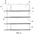
- FIG. 6 is a zoom-in view of an area B in FIG. 4 .
- a total length of portions of the signal line G 2 crossing over corresponding second apertures is substantially same as a total length of portions of the signal line G 1 , which means that the second apertures between the two adjacent first apertures has a length along the second direction D 2 substantially same as lengths of the two adjacent first apertures along the second direction, so signal coupling on the portion of the respective first touch-sensing electrode corresponding to the signal line G 2 and the portion of the respective first touch-sensing electrode corresponding to the signal line G 1 (or signal line G 3 , or signal line G 4 ) are substantially same.
- FIG. 7 is a zoom-in view of an area B in FIG. 4 .
- the touch-sensing display substrate further includes a plurality of connecting lines CL.
- a respective one of the plurality of connecting lines CL is electrically connected to a corresponding first touch-sensing electrode.
- the respective one of the plurality of connecting lines CL is electrically connected to the corresponding first touch-sensing electrode in parallel.
- the arrangement of the plurality of second apertures 102 and the plurality of connecting lines CL not only ensures that the total length of portions of the first signal line crossing over the plurality of first apertures is substantially same as the total length of portions of the second signal line crossing over the plurality of second apertures, but also avoid the electrical resistance of the respective one of the plurality of first touch-sensing electrodes from increasing.
- the touch-sensing display substrate includes a plurality of subpixel region SP and an inter-subpixel region ISR.
- a subpixel region SP refers to a light emission region of a subpixel, such as a region corresponding to a pixel electrode in a liquid crystal display, a region corresponding to a light emissive layer in an organic light emitting diode display panel, or a region corresponding to the light transmission layer in the present disclosure.
- a pixel may include a number of separate light emission regions corresponding to a number of subpixels in the pixel.
- the subpixel region is a light emission region of a red color subpixel.
- the subpixel region is a light emission region of a green color subpixel.
- the subpixel region is a light emission region of a blue color subpixel.
- the subpixel region is a light emission region of a white color subpixel.
- an inter-subpixel region ISR refers to a region between adjacent subpixel regions, such as a region corresponding to a black matrix in a liquid crystal display, a region corresponding a pixel definition layer in an organic light emitting diode display panel, or a black matrix in the present display panel.
- the inter-subpixel region is a region between adjacent subpixel regions in a same pixel.
- the inter-subpixel region is a region between two adjacent subpixel regions from two adjacent pixels.
- the inter-subpixel region is a region between a subpixel region of a red color subpixel and a subpixel region of an adjacent green color subpixel.
- the inter-subpixel region is a region between a subpixel region of a red color subpixel and a subpixel region of an adjacent blue color subpixel.
- the inter-subpixel region is a region between a subpixel region of a green color subpixel and a subpixel region of an adjacent blue color subpixel.
- a respective one of the plurality of subpixel regions SP is a light transmitting region.
- the inter-subpixel region ISP is a light blocking region.
- the respective one of the plurality of subpixel regions SP is a light emitting region.
- the inter-subpixel region ISP is not a light emitting region.
- the plurality of connecting lines CL extends through both one of the plurality of subpixel regions SP and the inter-subpixel region ISR.
- a respective one of the plurality of connecting lines CL extends through one of the plurality of subpixel regions SP.
- a respective one of the plurality of connecting lines CL extends through the inter-subpixel region ISR but without extending through the plurality of subpixel regions SP, which can avoid adverse effect of the plurality of connecting lines CL in the display quality (e.g., display non-uniformity).
- FIG. 94 is a schematic diagram of a structure of a touch-sensing display substrate in some embodiments according to the present disclosure.
- FIG. 9B is a schematic diagram of a structure of a touch-sensing display substrate in some embodiments according to the present disclosure.
- the plurality of connecting lines CL includes a plurality of first connecting lines CL 1 and a plurality of second connecting lines CL 2 .
- a plurality of first connecting lines CL 1 are arranged along the first direction D 1 and disposed in the inter-subpixel region ISR of the touch-sensing display substrate.
- a respective one of the plurality of first connecting lines CL 1 extends along the second direction D 2 and is electrically connected to a corresponding first touch-sensing electrode.
- multiple lines of the plurality of first connecting lines CL 1 are electrically connected in parallel to each other.
- the plurality of first connecting lines CL 1 are parallel to a plurality of gate lines.
- the plurality of first connecting lines CL 1 and the plurality of gate lines are in a same layer and includes a same material, which simplify the process of fabricating the touch-sensing display apparatus.
- the plurality of second connecting lines CL 2 are arranged along the second direction D 2 and disposed in the inter-subpixel region ISR of the touch-sensing display substrate.
- the respective one of the plurality of first touch-sensing electrodes 10 is electrically connected to the plurality of second connecting lines CL 2 .
- multiple lines of the plurality of second connecting lines CL 2 are electrically connected in parallel to each other.
- the plurality of second connecting lines CL 2 are parallel to a plurality of data lines.
- the plurality of second connecting lines CL 2 and the plurality of data lines are in a same layer and include a same material, which simplify the process of fabricating the touch-sensing display apparatus.
- a respective one of the plurality of second connecting lines CL 2 is electrically connected to end of at least one of the plurality of first connecting lines CL 1 .
- an orthographic projection of the respective one of the plurality of first touch-sensing electrodes 10 on a base substrate 00 at least partially overlaps with an orthographic projection of the at least one of the plurality of first connecting lines CL 1 electrically connected to the respective one of the plurality of second connecting lines on the base substrate 00 .
- the respective one of the plurality of first connecting lines CL 1 is electrically connected to the corresponding first touch-sensing electrode.
- the corresponding first touch-sensing electrode is electrically connected to the plurality of second connecting lines CL 2 .
- the respective one of the plurality of first connecting lines CL 1 is electrically connected to the corresponding first touch-sensing electrode through at least one first connecting via.
- the respective one of the plurality of second connecting lines CL 2 is electrically connected to the corresponding first touch-sensing electrode through at least one second connecting via.
- the at least one first connecting via and the at least one second connecting via are different vias.
- lots of vias formed on the touch-sensing display substrate may increase difficulties of fabricating the touch-sensing display substrate. And lots of vias may have an adverse effect on the display quality.
- FIG. 10 is a schematic diagram of a structure of a touch-sensing display substrate in some embodiments according to the present disclosure.
- FIG. 11A is a cross-sectional view of a touch-sensing display substrate along a CC direction in FIG. 10 .
- the touch-sensing display substrate further includes a first insulating layer 5 between the plurality of gate lines 1 and the plurality of data lines 2 .
- one of the plurality of first connecting lines CL 1 and one of the plurality of second connecting lines CL 2 are electrically connected with each other though one of the plurality of first connecting vias 51 extending through the first insulating layer 5 .
- the touch-sensing display substrate further includes a second insulating layer 6 between the plurality of data lines 2 and the plurality of first touch-sensing electrodes 10 . Since the plurality of second connecting lines CL 2 and the plurality of data lines 2 are in the same layer, the second insulating layer 6 is between the plurality of second connecting lines CL 2 and the plurality of first touch-sensing electrodes 10 .
- the plurality of second connecting lines CL 2 respectively extend through the second insulating layer 6 to electrically connect to the plurality of first touch-sensing electrodes 10 respectively through a plurality of second connecting vias 61 extending through the second insulating layer 6 .
- the plurality of first connecting lines CL 1 are respective electrically connected to the plurality sf second connecting lines CL 2 , and the plurality of second connecting lines CL 2 are respectively electrically connected to the plurality of first touch-sensing electrodes 10 , the plurality of first connecting lines CL 1 are respectively electrically connected to the plurality of first touch-sensing electrodes 10 .
- the plurality of first connecting vias 51 and one of the plurality of second connecting vias 61 By using one of the plurality of first connecting vias 51 and one of the plurality of second connecting vias 61 , one of the plurality of first connecting lines CL 1 , one of the plurality of second connecting lines CL 2 , and one of the plurality of first touch-sensing electrodes 10 are respectively connected, which simplify the process of fabricating the touch-sensing display substrate.
- the touch-sensing display substrate further include a second insulating layer 6 between the plurality of gate lines 1 and the plurality of first touch-sensing electrodes 10 . Since the plurality of first connecting lines CL 1 and the plurality of gate lines 1 are in the same layer, the second insulating layer 6 is between the plurality of first connecting lines CL 1 and the plurality of first touch-sensing electrodes 10 .
- the plurality of first connecting lines CL 1 respectively extend through the second insulating layer 6 to electrically connect to the plurality of first touch-sensing electrodes 10 through a plurality of second connecting vias 61 extending through the second insulating layer 6 .
- the plurality of first connecting lines CL 1 are respectively electrically connected to the plurality of second connecting lines CL 2
- the plurality of first connecting liens CL 1 are respectively electrically connected to the plurality of first touch-sensing electrodes 10
- the plurality of second connecting lines CL 2 are respectively electrically connected to the plurality of first touch-sensing electrodes 10 .
- one of the plurality of first connecting vias 51 and one of the plurality of second connecting vias 61 one of the plurality of first connecting lines CL 1 , one of the plurality of second connecting lines CL 2 , and one of the plurality of first touch-sensing electrodes 10 are respectively connected, which simplify the process of fabricating the touch-sensing display substrate.
- a region R 51 corresponding to a respective one of the plurality of first connecting vias 51 at least partially overlaps with a region R 61 corresponding to a respective one of the plurality of second connecting vias 61 , which decreases an area of regions having the plurality of first connecting vias 51 and the plurality of second connecting vias 61 , and decreases the adverse effect of the plurality of first connecting vias 51 and the plurality of second connecting vias 61 on the display quality.
- the touch-sensing display substrate includes a plurality of first connecting lines CL 1 arranged along the first direction D 1 and disposed in an inter-subpixel region ISR of the touch-sensing display substrate; and a plurality of second connecting lines CL 2 arranged along the second direction D 2 and disposed in the inter-subpixel region ISR of the touch-sensing display substrate.
- a respective one of the plurality of first connecting lines CL 1 extends along the second direction D 2 and is electrically connected to the respective one of the plurality of first touch-sensing electrodes 10 .
- the respective one of the plurality of first touch-sensing electrodes 10 is electrically connected to the plurality of second connecting lines CL 2 .
- the plurality of first connecting lines CLT are parallel to a plurality of gate lines 1 .
- the plurality of second connecting lines CL 1 are parallel to a plurality of data lines 2 .
- the touch-sensing display substrate further includes a first insulating layer 5 between the plurality of gate lines 1 and the plurality of data lines 2 .
- a respective one of the plurality of second connecting lines CL 2 extends through the first insulating layer 5 and electrically connects to ends of at least one of the plurality of first connecting lines CL 1 .
- an orthographic projection of the respective one of the plurality of first touch-sensing electrodes 10 on a base substrate 00 at least partially overlaps with an orthographic projection of the at least one of the plurality of first connecting lines CL 1 electrically connected to the respective one of the plurality of second connecting lines CL 2 on the base substrate 00 .
- the plurality of gate lines 1 and the plurality of data lines 2 defines the plurality of subpixel regions SP.
- a respective one of the plurality of subpixel regions SP includes a pixel electrode.
- the touch-sensing display substrate is used in an electroluminescent display apparatus e.g., OLED
- the respective one of the plurality of subpixel regions SP includes an anode.
- the touch-sensing display substrate includes a plurality of thin film transistors 4 .
- a respective one of the plurality of thin film transistors 4 includes a source electrode, a drain electrode, an active layer, a gate electrode, and a gate insulating layer.
- the drain electrode of the respective one of the plurality of thin film transistors 4 is electrically connected to the pixel electrode or the anode.
- the source electrode of the respective one of the plurality of thin film transistors 4 is electrically connected to the respective one of the plurality of data lines 2 .
- the first insulating layer 5 and the gate insulating layer of the plurality of thin film transistors 4 are in a same layer and include a same material. So, the first insulating layer 5 and the gate insulating layer of the plurality of thin film transistors 4 can be formed in a same process, which simplifies the process of fabricating the touch-sensing display substrate.
- the second insulating layer 6 and a planarization layer of the plurality of thin film transistors 4 are in a same layer and include a same material.
- the planarization layer includes resin. So, the second insulating layer 6 and a planarization layer of the plurality of thin film transistors 4 can be formed in a same process, which simplifies the process of fabricating the touch-sensing display substrate.
- an insulating layer is formed between the common electrode and the pixel electrode or between the common electrode and the anode.
- FIG. 12 is a zoom-in view of an area B in FIG. 4 .
- the common electrode e.g., the plurality of first touch-sensing electrodes 10 and the plurality of second touch-sensing electrodes 20
- the touch-sensing display substrate further includes a plurality of third apertures 104 .
- a first portion of the plurality of third apertures 104 extend through a respective one of the plurality of first touch-sensing electrodes 10 .
- a second portion of the plurality of third apertures 104 extend through a respective one of the plurality of second touch-sensing sub-electrodes 201 .
- the pixel electrode or the anode is electrically connected to the drain electrode of the respective one of the plurality of thin film transistors 4 through a respective one of the plurality of the third apertures 104 .
- the first portion of the plurality of third apertures 104 are included in the plurality of second apertures extending through the respective one of the plurality of first touch-sensing electrodes 10 .
- the respective one of the plurality of second apertures 102 is connected with at least one of the first portion of the plurality of third aperture 104 .
- the touch-sensing display substrate further includes a plurality of fourth apertures 105 extending through the plurality of first touch-sensing electrodes 10 and loads of the plurality of second touch-sensing electrodes 20 .
- FIG. 13 is a schematic diagram of a structure of a touch-sensing display substrate in some embodiments according to the present disclosure.
- the plurality of first connecting lines CL and the plurality of second connecting lines CL 2 are electrically connected.
- the plurality of first connecting lines CLT are electrically connected.
- the plurality of the second connecting lines CL 2 are electrically connected.
- the plurality of first connecting lines CL 1 are electrically connected, so, the plurality of first connecting lines CL 1 are short.
- the plurality of second connecting lines CL 2 are electrically connected, so, the plurality of second connecting lines CL 2 are short. Because the respective one of the plurality of first touch-sensing electrodes 10 are electrically connected to at least one of the plurality of first connecting lines CL 1 and to at least one of the plurality of second connecting lines CL 2 , the electrical resistance of the respective one of the plurality of first touch-sensing electrodes 10 is further reduces.
- the touch-sensing display substrate further includes a plurality of first touch-sensing signal lines 30 arranged along the second direction D 2 ; and a plurality of second touch-sensing signal lines 40 arranged along the second direction D 2 .
- a respective one of the plurality of first touch-sensing signal lines 30 and a respective one of the plurality of second touch-sensing signal lines 40 extend along the first direction D 1 .
- the respective one of the plurality of first touch-sensing signal lines 30 is electrically connected to the respective one of the plurality of first touch-sensing electrodes 10 .
- the respective one of the plurality of second touch-sensing signal lines 40 is electrically connected to the respective one of the plurality of second touch-sensing electrodes 20 .
- the plurality of second touch-sensing sub-electrodes 201 are arranged in array.
- the plurality of second touch-sensing sub-electrodes 201 in the respective one of the plurality of second touch-sensing electrodes 20 are arranged in an 8 ⁇ 4 array.
- the plurality of data lines 2 extend along the first direction D 1 .
- the plurality of first touch-sensing signal lines 30 , the plurality of second touch-sensing signal lines 40 , and the plurality of data lines 2 are in a same layer and include a same material.
- the plurality of first touch-sensing signal lines 30 , the plurality of second touch-sensing signal lines 40 , and the plurality of data lines 2 are parallel to each other. So, the plurality of first touch-sensing signal lines 30 , the plurality of second touch-sensing signal lines 40 , and the plurality of data lines 2 can be formed in a same process.
- the plurality of first touch-sensing electrodes 10 and the plurality of second touch-sensing electrodes 20 are in a same layer and include a same material.
- the plurality of first touch-sensing electrodes 10 and the plurality of second touch-sensing electrodes 20 are in different layers.
- the plurality of data lines 2 is closer to the plurality of second touch-sensing electrodes 20 , the plurality of first touch-sensing electrodes 10 and the plurality of second touch-sensing electrodes 20 are in a same layer and include a same material. Referring to FIG. 10 and FIG.
- vias are formed extending through the second insulating layer 6 between the plurality of second touch-sensing electrodes 20 and the plurality of second touch-sensing signal lines 40 , no via is formed in the first insulating layer 5 between the plurality of data lines 2 and the plurality of gate lines 1 , so the respective one of the plurality of second touch-sensing electrodes 20 are electrically connected to the respective one of the plurality of second touch-sensing signal lines 40 , the respective one of the plurality of second touch-sensing electrodes 20 is insulated from the plurality of gate lines 1 and the plurality of connecting lines parallel to the plurality of gate lines.
- the plurality of first connecting lines CL 1 is parallel to the plurality of gate lines 1
- the plurality of second touch-sensing electrodes 20 are insulated from the plurality of first connecting lines CL 1 .
- the plurality of first touch-sensing signal lines 30 and the plurality of second touch-sensing signal lines 40 extend along the first direction D 1 , an integrated circuit can be disposed on a side of the touch-sensing display substrate to perform driving from a single side, which can narrow the frame of the display apparatus.
- the touch-sensing structure includes a plurality of first touch-sensing electrodes 10 arranged along a first direction D 1 and extending along a second direction D 2 .
- the touch-sensing structure further includes a plurality of second touch-sensing electrodes 20 arranged along the second direction D 2 and extending along the first direction D 1 ; and a plurality of second touch-sensing signal lines 40 extending along the first direction D 1 .
- a respective one of the plurality of second touch-sensing signal lines 40 is electrically connected to a corresponding second touch-sensing electrode (e.g., one of the plurality of second touch-sensing electrodes 20 ).
- the first direction D 1 is different from the second direction D 2 .
- the respective one of the plurality of second touch-sensing signal lines 40 is substantially parallel to the plurality of second touch-sensing electrodes 20 .
- an orthographic projection of the respective one of the plurality of second touch-sensing signal lines 40 on a base substrate 00 at least partially overlaps with an orthographic projection of the one of the plurality of second touch-sensing electrodes 20 on the base substrate 00 .
- the respective one of the plurality of first touch-sensing electrodes 10 is insulated from the plurality of second touch-sensing electrodes 20 .
- the respective one of the plurality of second touch-sensing electrodes 20 is insulated from the plurality of first touch-sensing electrodes 10 .
- the respective one of the plurality of first touch-sensing electrodes 10 is a transmitting (TX) electrode (e.g., a scanning electrode), and the respective one of the plurality of second touch-sensing electrodes 20 is a receiving (RX) electrode (e.g., a sensing electrode).
- TX transmitting
- RX receiving
- the respective one of the plurality of first touch-sensing signal lines 30 electrically connected to the corresponding first touch-sensing electrode is a transmitting line (TX line).
- the respective one of the plurality of second touch-sensing signal lines 40 electrically connected to the corresponding second touch-sensing electrode is a receiving line (RX line).
- the respective one of the plurality of second touch-sensing electrodes 20 is a transmitting (TX) electrode
- the respective one of the plurality of first touch-sensing electrodes 10 is a receiving (RX) electrode.
- the plurality of first touch-sensing electrodes 10 and the plurality of second touch-sensing electrodes 20 are in different layers.
- the plurality of first touch-sensing electrodes 10 are insulated from the plurality of second touch-sensing electrodes 20 using an insulating layer.
- the plurality of first touch-sensing electrodes 10 and the plurality of second touch-sensing electrodes 20 are in a same layer, the plurality of first touch-sensing electrodes 10 and the plurality of second touch-sensing electrodes 20 can be formed within a same process, which can simplify the process of fabricating the touch-sensing substrate.
- the term “same layer” refers to the relationship between the layers simultaneously formed in the same step.
- the plurality of first touch-sensing electrodes 10 and the plurality of second touch-sensing electrodes 20 are in a same layer when they are formed as a result of one or more steps of a same patterning process performed in a same layer of material.
- the plurality of first touch-sensing electrodes 10 and the plurality of second touch-sensing electrodes 20 can be formed in a same layer by simultaneously performing the step of forming the plurality of first touch-sensing electrodes 10 and the step of forming the plurality of second touch-sensing electrodes 20 .
- the term “same layer” does not always mean that the thickness of the layer or the height of the layer in a cross-sectional view is the same.
- the respective one of the plurality of first touch-sensing electrodes is an integral portion including a plurality of first touch-sensing sub-electrodes connected together
- the respective one of the plurality of second touch-sensing electrodes includes a plurality of second touch-sensing sub-electrodes 201 spaced apart from each other.
- a column of second touch-sensing sub-electrodes of the plurality of second touch-sensing sub-electrodes in the respective one of the plurality of second touch-sensing electrodes are connected by bridges (e.g., signal lines, signal wires). The bridges are insulated from the plurality of first touch-sensing electrodes.
- the touch-sensing display substrate further includes a plurality of first apertures 101 respectively extending through a thickness of the respective one of the plurality of first touch-sensing electrodes 10 .
- the plurality of first apertures 101 are arranged in multiple rows.
- the respective one of the plurality of second touch-sensing electrodes 20 includes a plurality of second touch-sensing sub-electrodes 201 .
- the plurality of second touch-sensing sub-electrodes 201 are arranged in multiple columns.
- a respective second touch-sensing sub-electrodes 201 is in a region corresponding to a respective first apertures 101 .
- the plurality of first apertures 101 are arranged in one row.
- the plurality of second touch-sensing sub-electrodes 201 are arranged in one column. In a region where a row region corresponding to the plurality of first apertures 101 overlaps with a column region corresponding to the plurality of second touch-sensing sub-electrodes 201 , a respective second touch-sensing sub-electrodes 201 is in a region corresponding to a respective first apertures 101 .
- the plurality of first touch-sensing electrodes 10 and the plurality of second touch-sensing electrodes 20 can be formed in a same layer.
- the plurality of first touch-sensing electrodes 10 and the plurality of second touch-sensing electrodes 20 can be formed in the same process.
- an insulating layer is absent between the plurality of first touch-sensing electrodes 10 and the plurality of second touch-sensing electrodes 20 . So, the process of fabricating the touch-sensing display substrate is simplified, and the efficiency of fabricating the touch-sensing display substrate is improved.
- the plurality of first touch-sensing electrodes 10 and the plurality of second touch-sensing electrodes 20 are formed in a same layer, the plurality of first touch-sensing electrodes 10 and the plurality of second touch-sensing electrodes 20 can be used as a common electrode when the display substrate displays an image. So, the plurality of first touch-sensing electrodes 10 and the plurality of second touch-sensing electrodes 20 are not only used to perform a touch-control function, but also used to perform a display function.
- the touch control function and the display function can be performed at the same time, which can obviate the issue of insufficient charging time of data lines, if the touch control function and the display function are performed in a time division fashion, the data line may not be sufficiently charged during the limited charging period. The problem becomes particularly severe in high resolution display panels.
- the present apparatus is compatible with an active pen.
- the touch-sensing structure 100 further includes a plurality of first touch-sensing signal lines 30 and a plurality of second touch-sensing signal lines 40 .
- the plurality of first touch-sensing signal lines 30 and the plurality of second touch-sensing signal lines 40 extend along a same direction.
- the plurality of first touch-sensing signal lines 30 and the plurality of second touch-sensing signal lines 40 extend along the first direction D 1 .
- the plurality of second touch-sensing electrodes 20 extends along a same direction (e.g., the first direction D along which the plurality of second touch-sensing signal lines 40 extend.
- the respective one of the plurality of second touch-sensing signal lines 40 connects a column of second touch-sensing sub-electrodes of the plurality of second touch-sensing sub-electrodes 201 in the respective one of the plurality of second touch-sensing electrodes 20 .
- a plurality of touch-sensing vias 60 extending through an insulating layer, between the plurality of second touch-sensing electrodes 20 and the plurality of second touch-sensing signal lines 40 , are evenly distributed on the insulating layer to allow the respective one of the plurality of second touch-sensing signal lines 40 to be electrically connected to the corresponding second touch-sensing electrode.
- a plurality of touch-sensing vias 60 are evenly distributed in regions where the plurality of second touch-sensing signal lines 40 crosses through the plurality of second touch-sensing electrodes 20 .
- the evenly distributed touch-sensing vias 60 will avoid the display uniformity problem and improve the display quality of the touch-sensing display substrate.
- the plurality of first touch-sensing electrodes 10 are arranged in array.
- an array of the plurality of first touch-sensing electrodes 10 has m rows and n columns, wherein m and n are positive integers, m ⁇ 2, n ⁇ 2.
- the array of the plurality of first touch-sensing electrodes 10 has 80 rows and 100 columns.
- the plurality of first touch-sensing electrodes 10 can be used as a common electrode.
- the touch control function and the display function can be performed by the touch-sensing display substrate.
- using the plurality of first touch-sensing electrodes 10 as the common electrode can reduce a thickness of the touch-sensing display substrate.
- the plurality of first touch-sensing electrodes and the plurality of second touch-sensing electrodes are substantially transparent.
- substantially transparent means at least 50 percent (e.g., at least 60 percent, at least 70 percent, at least 80 percent, at least 90 percent, and at least 95 percent) of an incident light in the visible wavelength range transmitted therethrough.
- Various appropriate electrode materials and various appropriate fabricating methods may be used to make the plurality of first touch-sensing electrodes and the plurality of second touch-sensing electrodes.
- Examples of appropriate electrode materials for making the plurality of first touch-sensing electrodes and the plurality of second touch-sensing electrodes include, but are not limited to, Indium Tin Oxide (ITO), and Indium Zinc Oxide (IZO).
- the present disclosure also provides a touch-sensing display apparatus.
- the touch-sensing display apparatus includes a touch-sensing display substrate described herein.
- the touch-sensing display apparatus is operated in a time division mode including a display mode and a touch control mode.
- the plurality of first touch-sensing electrodes are used as a common electrode and are configured to be provided with a common voltage.
- the plurality of first touch-sensing electrodes and the plurality of second touch-sensing electrodes are used as the common electrode.
- the plurality of first touch-sensing electrodes are a plurality of touch sensing electrodes configured to transmit touch signals.
- the plurality of second touch-sensing electrodes are a plurality of touch scanning electrodes configured to provide a scanning signal.
- the touch-sensing display apparatus includes one or more integrated circuits connected to the touch-sensing display substrate.
- appropriate touch-sensing display apparatuses include, but are not limited to, an electronic paper, a mobile phone, a tablet computer, a television, a monitor, a notebook computer, a digital album, a GPS, wireless devices, personal data assistants (PDAs), handheld or portable computers, GPS receivers/navigators, cameras, MP4 video players, camcorders, game consoles, watches, clocks, calculators, TV monitors flat panel display, computer monitor, car display (e.g., odometer display, etc.), navigator, cockpit controller and/or display, camera view display (e.g., rear view camera display in a vehicle), electronic photo, electronic Billboards or signs, projectors, architectural structures, packaging, and aesthetic structures (e.g., displays for images of a piece of jewelry), etc.
- PDAs personal data assistants
- GPS receivers/navigators cameras
- the present disclosure also provides a method of operating a touch sensing display apparatus.
- the method of operating a touch sensing display apparatus includes operating a touch sensing display apparatus described herein in a time division mode including a display mode and a touch control mode.
- the plurality of first touch-sensing electrodes are used as a common electrode and are configured to be provided with a common voltage.
- the plurality of first touch-sensing electrodes and the plurality of second touch-sensing electrodes are used as the common electrode.
- the plurality of first touch-sensing electrodes are a plurality of touch sensing electrodes configured to transmit touch signals.
- the plurality of second touch-sensing electrodes are a plurality of touch scanning electrodes configured to provide a scanning signal.
- the present disclosure also provides a method of fabricating a touch-sensing display substrate.
- the method of fabricating a touch-sensing display substrate includes forming a plurality of first touch-sensing electrodes arranged along a first direction, a respective one of the plurality of first touch-sensing electrodes extending along a second direction different from the first direction; forming a plurality of first apertures respectively extending through a thickness of a respective one of the plurality of first touch-sensing electrodes, the plurality of first apertures arranged along the second direction; a plurality of second apertures respectively extending through of a thickness of the respective one of the plurality of first touch-sensing electrodes the plurality of second apertures arranged along the second direction; and forming a plurality of signal lines.
- a first signal line of the plurality of signal lines is formed to extend along the second direction and crosses over the plurality of first apertures in one of the plurality of first touch-sensing electrodes but not the plurality of second apertures in any first touch-sensing electrode.
- a second signal line of the plurality of signal lines is formed to extend along the second direction and crosses over the plurality of second apertures in a same as or different from the one of the plurality of first touch-sensing electrodes crossed-over by the first signal line, but not the plurality of first apertures in any first touch-sensing electrode.
- the term “the invention”, “the present invention” or the like does not necessarily limit the claim scope to a specific embodiment, and the reference to exemplary embodiments of the invention does not imply a limitation on the invention, and no such limitation is to be inferred.
- the invention is limited only by the spirit and scope of the appended claims. Moreover, these claims may refer to use “first”, “second”, etc. following with noun or element. Such terms should be understood as a nomenclature and should not be construed as giving the limitation on the number of the elements modified by such nomenclature unless specific number has been given.
Abstract
Description
Claims (20)
Applications Claiming Priority (5)
| Application Number | Priority Date | Filing Date | Title |
|---|---|---|---|
| CN201910143211.3A CN110442255B (en) | 2019-02-26 | 2019-02-26 | Touch substrate and touch display device |
| CN201910142492.0 | 2019-02-26 | ||
| CN201910143211.3 | 2019-02-26 | ||
| CN201910142492.0A CN110442254B (en) | 2019-02-26 | 2019-02-26 | Touch display substrate and touch display device |
| PCT/CN2019/106241 WO2020173082A1 (en) | 2019-02-26 | 2019-09-17 | Touch-sensing display substrate, touch-sensing display apparatus, method of operating touch sensing display apparatus, and method of fabricating touch-sensing display substrate |
Publications (2)
| Publication Number | Publication Date |
|---|---|
| US20210232265A1 US20210232265A1 (en) | 2021-07-29 |
| US11216128B2 true US11216128B2 (en) | 2022-01-04 |
Family
ID=72238969
Family Applications (2)
| Application Number | Title | Priority Date | Filing Date |
|---|---|---|---|
| US16/638,437 Active 2039-10-25 US11216128B2 (en) | 2019-02-26 | 2019-09-17 | Touch-sensing display substrate, touch-sensing display apparatus, method of operating touch sensing display apparatus, and method of fabricating touch-sensing display substrate |
| US16/638,436 Active 2039-10-09 US11099693B2 (en) | 2019-02-26 | 2019-09-17 | Touch-sensing display substrate, touch-sensing display apparatus, method of operating touch-sensing display apparatus, and method of fabricating touch-sensing display substrate |
Family Applications After (1)
| Application Number | Title | Priority Date | Filing Date |
|---|---|---|---|
| US16/638,436 Active 2039-10-09 US11099693B2 (en) | 2019-02-26 | 2019-09-17 | Touch-sensing display substrate, touch-sensing display apparatus, method of operating touch-sensing display apparatus, and method of fabricating touch-sensing display substrate |
Country Status (2)
| Country | Link |
|---|---|
| US (2) | US11216128B2 (en) |
| WO (2) | WO2020173081A1 (en) |
Families Citing this family (3)
| Publication number | Priority date | Publication date | Assignee | Title |
|---|---|---|---|---|
| CN105934734B (en) | 2014-01-22 | 2020-11-20 | 株式会社和冠 | Position indicator, position detection device, position detection circuit, and position detection method |
| CN111708464B (en) * | 2020-06-30 | 2022-09-09 | 厦门天马微电子有限公司 | Touch display panel and touch display device |
| TWI825692B (en) * | 2022-04-27 | 2023-12-11 | 友達光電股份有限公司 | Touch display device and driving method |
Citations (21)
| Publication number | Priority date | Publication date | Assignee | Title |
|---|---|---|---|---|
| US20120139866A1 (en) * | 2010-12-02 | 2012-06-07 | Suk-Won Jung | Display substrate, method of manufacturing the same and touch-detecting display apparatus having the same |
| CN103294312A (en) | 2013-05-15 | 2013-09-11 | 京东方科技集团股份有限公司 | Capacitive touch screen, production method of capacitive touch screen and display device |
| US20140104221A1 (en) * | 2012-10-11 | 2014-04-17 | Maxim Integrated Products, Inc. | Capacitive touch panel sensor for mitigating effects of a floating condition |
| CN104020893A (en) | 2014-05-30 | 2014-09-03 | 京东方科技集团股份有限公司 | In cell touch panel and display device |
| CN104102402A (en) | 2014-06-25 | 2014-10-15 | 京东方科技集团股份有限公司 | Touch substrate and display device |
| CN104503648A (en) | 2015-01-09 | 2015-04-08 | 京东方科技集团股份有限公司 | Embedded type touch screen and display device |
| CN104503650A (en) | 2015-01-15 | 2015-04-08 | 京东方科技集团股份有限公司 | Embedded touch screen and display device |
| CN104571765A (en) | 2015-01-09 | 2015-04-29 | 京东方科技集团股份有限公司 | In-cell touch panel and display device |
| JP2015108896A (en) | 2013-12-03 | 2015-06-11 | 大日本印刷株式会社 | Touch panel electrode substrate, touch panel device, and manufacturing method of touch panel electrode substrate |
| CN104915078A (en) | 2014-03-14 | 2015-09-16 | 三星显示有限公司 | Touch panel and display device including the same |
| CN104965622A (en) | 2015-04-01 | 2015-10-07 | 上海天马微电子有限公司 | Array substrate and display panel |
| CN205810812U (en) | 2016-07-22 | 2016-12-14 | 京东方科技集团股份有限公司 | A kind of array base palte and display device |
| JP2017134340A (en) | 2016-01-29 | 2017-08-03 | 京セラディスプレイ株式会社 | Liquid crystal display device with touch panel |
| US20170269746A1 (en) * | 2015-09-07 | 2017-09-21 | Boe Technology Group Co., Ltd. | In-cell touch screen and display device |
| CN108319398A (en) | 2018-02-28 | 2018-07-24 | 京东方科技集团股份有限公司 | A kind of touch panel and preparation method thereof, touch device |
| US20190005923A1 (en) | 2015-04-30 | 2019-01-03 | Lg Display Co., Ltd. | Touch Recognition Enabled Display Device with Asymmetric Black Matrix Pattern |
| CN109212839A (en) | 2018-11-26 | 2019-01-15 | 昆山龙腾光电有限公司 | The control method of array substrate, display device and display device |
| US20190113410A1 (en) * | 2017-10-17 | 2019-04-18 | University Of Maryland, College Park | Two-dimensional center of pressure sensor systems, devices, and methods |
| US20200089037A1 (en) * | 2018-09-19 | 2020-03-19 | Sharp Kabushiki Kaisha | Method for manufacturing active matrix substrate and method for manufacturing liquid crystal display device with touch sensor |
| US20200089038A1 (en) * | 2018-09-19 | 2020-03-19 | Sharp Kabushiki Kaisha | Active matrix substrate and liquid crystal display device with touch sensor using the same |
| US20210117031A1 (en) * | 2019-10-22 | 2021-04-22 | Sharp Kabushiki Kaisha | Display device including position input function |
Family Cites Families (7)
| Publication number | Priority date | Publication date | Assignee | Title |
|---|---|---|---|---|
| US7932898B2 (en) * | 2005-09-20 | 2011-04-26 | Atmel Corporation | Touch sensitive screen |
| CN104142772B (en) * | 2014-07-24 | 2017-05-03 | 京东方科技集团股份有限公司 | Embedded type touch screen and display device |
| CN104536637A (en) * | 2015-01-29 | 2015-04-22 | 京东方科技集团股份有限公司 | Embedded touch screen and display device |
| CN110083262B (en) * | 2015-01-30 | 2022-07-26 | 乐金显示有限公司 | Touch display device |
| US9939972B2 (en) * | 2015-04-06 | 2018-04-10 | Synaptics Incorporated | Matrix sensor with via routing |
| CN106055160B (en) | 2016-06-24 | 2019-12-27 | 京东方科技集团股份有限公司 | Array substrate, preparation method thereof, display panel and display device |
| CN106201114B (en) | 2016-08-26 | 2019-03-12 | 京东方科技集团股份有限公司 | Touch-control structure, array substrate and display device |
-
2019
- 2019-09-17 US US16/638,437 patent/US11216128B2/en active Active
- 2019-09-17 WO PCT/CN2019/106200 patent/WO2020173081A1/en active Application Filing
- 2019-09-17 WO PCT/CN2019/106241 patent/WO2020173082A1/en active Application Filing
- 2019-09-17 US US16/638,436 patent/US11099693B2/en active Active
Patent Citations (29)
| Publication number | Priority date | Publication date | Assignee | Title |
|---|---|---|---|---|
| US20120139866A1 (en) * | 2010-12-02 | 2012-06-07 | Suk-Won Jung | Display substrate, method of manufacturing the same and touch-detecting display apparatus having the same |
| US20140104221A1 (en) * | 2012-10-11 | 2014-04-17 | Maxim Integrated Products, Inc. | Capacitive touch panel sensor for mitigating effects of a floating condition |
| CN103294312A (en) | 2013-05-15 | 2013-09-11 | 京东方科技集团股份有限公司 | Capacitive touch screen, production method of capacitive touch screen and display device |
| US20150153875A1 (en) | 2013-05-15 | 2015-06-04 | Boe Technology Group Co., Ltd. | Capacitive touch panel, manufacturing method of capacitive touch panel and display device |
| JP2015108896A (en) | 2013-12-03 | 2015-06-11 | 大日本印刷株式会社 | Touch panel electrode substrate, touch panel device, and manufacturing method of touch panel electrode substrate |
| US20150261348A1 (en) | 2014-03-14 | 2015-09-17 | Samsung Display Co., Ltd. | Touch panel and display device including the same |
| CN104915078A (en) | 2014-03-14 | 2015-09-16 | 三星显示有限公司 | Touch panel and display device including the same |
| CN104020893A (en) | 2014-05-30 | 2014-09-03 | 京东方科技集团股份有限公司 | In cell touch panel and display device |
| US20160274716A1 (en) | 2014-05-30 | 2016-09-22 | Boe Technology Group Co., Ltd. | In-cell touch panel and display device |
| CN104102402A (en) | 2014-06-25 | 2014-10-15 | 京东方科技集团股份有限公司 | Touch substrate and display device |
| US20150378390A1 (en) | 2014-06-25 | 2015-12-31 | Boe Technology Group Co., Ltd. | Touch Substrate and Display Device |
| US20160216802A1 (en) | 2015-01-09 | 2016-07-28 | Boe Technology Group Co., Ltd. | In-cell touch panel and display device |
| CN104571765A (en) | 2015-01-09 | 2015-04-29 | 京东方科技集团股份有限公司 | In-cell touch panel and display device |
| CN104503648A (en) | 2015-01-09 | 2015-04-08 | 京东方科技集团股份有限公司 | Embedded type touch screen and display device |
| US20160357312A1 (en) | 2015-01-09 | 2016-12-08 | Boe Technology Group Co., Ltd. | In cell touch panel and display device |
| CN104503650A (en) | 2015-01-15 | 2015-04-08 | 京东方科技集团股份有限公司 | Embedded touch screen and display device |
| US20160370917A1 (en) | 2015-01-15 | 2016-12-22 | Boe Technology Group Co., Ldt. | In-cell touch panel and display device |
| CN104965622A (en) | 2015-04-01 | 2015-10-07 | 上海天马微电子有限公司 | Array substrate and display panel |
| US20190005923A1 (en) | 2015-04-30 | 2019-01-03 | Lg Display Co., Ltd. | Touch Recognition Enabled Display Device with Asymmetric Black Matrix Pattern |
| US20170269746A1 (en) * | 2015-09-07 | 2017-09-21 | Boe Technology Group Co., Ltd. | In-cell touch screen and display device |
| JP2017134340A (en) | 2016-01-29 | 2017-08-03 | 京セラディスプレイ株式会社 | Liquid crystal display device with touch panel |
| CN205810812U (en) | 2016-07-22 | 2016-12-14 | 京东方科技集团股份有限公司 | A kind of array base palte and display device |
| US20190113410A1 (en) * | 2017-10-17 | 2019-04-18 | University Of Maryland, College Park | Two-dimensional center of pressure sensor systems, devices, and methods |
| CN108319398A (en) | 2018-02-28 | 2018-07-24 | 京东方科技集团股份有限公司 | A kind of touch panel and preparation method thereof, touch device |
| US20190265820A1 (en) | 2018-02-28 | 2019-08-29 | Boe Technology Group Co., Ltd. | Touch panel, method for fabricating the same, and touch device |
| US20200089037A1 (en) * | 2018-09-19 | 2020-03-19 | Sharp Kabushiki Kaisha | Method for manufacturing active matrix substrate and method for manufacturing liquid crystal display device with touch sensor |
| US20200089038A1 (en) * | 2018-09-19 | 2020-03-19 | Sharp Kabushiki Kaisha | Active matrix substrate and liquid crystal display device with touch sensor using the same |
| CN109212839A (en) | 2018-11-26 | 2019-01-15 | 昆山龙腾光电有限公司 | The control method of array substrate, display device and display device |
| US20210117031A1 (en) * | 2019-10-22 | 2021-04-22 | Sharp Kabushiki Kaisha | Display device including position input function |
Non-Patent Citations (2)
| Title |
|---|
| First Office Action in the Chinese Patent Application No. 201910143211.3, dated Apr. 17, 2019; English translation attached. |
| International Search Report & Written Opinion dated Dec. 20, 2019, regarding PCT/CN2019/106241. |
Also Published As
| Publication number | Publication date |
|---|---|
| US20210216164A1 (en) | 2021-07-15 |
| US20210232265A1 (en) | 2021-07-29 |
| US11099693B2 (en) | 2021-08-24 |
| WO2020173081A1 (en) | 2020-09-03 |
| WO2020173082A1 (en) | 2020-09-03 |
Similar Documents
| Publication | Publication Date | Title |
|---|---|---|
| US10908754B2 (en) | Touch sensing unit and display device including the same | |
| US11322551B2 (en) | Display panel and display device | |
| US10175797B2 (en) | Array substrate for OLED display panel, method for driving the same, and OLED display panel and display apparatus having the same | |
| WO2020135113A1 (en) | Array substrate, touch display panel, and touch display device | |
| US11216128B2 (en) | Touch-sensing display substrate, touch-sensing display apparatus, method of operating touch sensing display apparatus, and method of fabricating touch-sensing display substrate | |
| US10082903B2 (en) | Display panel and display device | |
| CN108010945B (en) | Display panel and display device | |
| US20170269762A1 (en) | Array substrate, related display panels, and related display apparatus | |
| US10025416B2 (en) | Display panel and method for forming the same | |
| CN110442254B (en) | Touch display substrate and touch display device | |
| US11231795B2 (en) | Touch control array substrate having a plurality of auxiliary conductive lines, and display apparatus thereof | |
| KR102585536B1 (en) | Array Substrate For Touch Display Device And Method Of Fabricating The Same | |
| US20190087033A1 (en) | Input-sensing device and display module including the same | |
| CN112864216A (en) | Display panel and electronic device | |
| CN114242759B (en) | Display panel and display device | |
| CN110767685A (en) | Display screen and display terminal | |
| US10732447B2 (en) | Touch panel and electronic device | |
| WO2019113956A1 (en) | Touch panel, touch substrate, and touch control display apparatus | |
| US20240061527A1 (en) | Touch sensing module and display device including the same | |
| CN220342752U (en) | Display device | |
| US20240069670A1 (en) | Touch detection module and display device including the same | |
| US11856816B2 (en) | Display panel and display device | |
| CN220709648U (en) | Display device | |
| US20220130945A1 (en) | Display Panel and Display Apparatus Using the Same | |
| US20230051888A1 (en) | Display device and sensing system including the same |
Legal Events
| Date | Code | Title | Description |
|---|---|---|---|
| FEPP | Fee payment procedure |
Free format text: ENTITY STATUS SET TO UNDISCOUNTED (ORIGINAL EVENT CODE: BIG.); ENTITY STATUS OF PATENT OWNER: LARGE ENTITY |
|
| AS | Assignment |
Owner name: BOE TECHNOLOGY GROUP CO., LTD., CHINA Free format text: ASSIGNMENT OF ASSIGNORS INTEREST;ASSIGNOR:ZHAO, TIANXIN;REEL/FRAME:052415/0774 Effective date: 20200210 Owner name: BEIJING BOE DISPLAY TECHNOLOGY CO., LTD., CHINA Free format text: ASSIGNMENT OF ASSIGNORS INTEREST;ASSIGNOR:ZHAO, TIANXIN;REEL/FRAME:052415/0774 Effective date: 20200210 Owner name: BOE TECHNOLOGY GROUP CO., LTD., CHINA Free format text: ASSIGNMENT OF ASSIGNORS INTEREST;ASSIGNOR:JI, HAOLIANG;REEL/FRAME:052415/0750 Effective date: 20200210 Owner name: BEIJING BOE DISPLAY TECHNOLOGY CO., LTD., CHINA Free format text: ASSIGNMENT OF ASSIGNORS INTEREST;ASSIGNOR:JI, HAOLIANG;REEL/FRAME:052415/0750 Effective date: 20200210 Owner name: BOE TECHNOLOGY GROUP CO., LTD., CHINA Free format text: ASSIGNMENT OF ASSIGNORS INTEREST;ASSIGNOR:WANG, SHIJUN;REEL/FRAME:052415/0714 Effective date: 20200210 Owner name: BEIJING BOE DISPLAY TECHNOLOGY CO., LTD., CHINA Free format text: ASSIGNMENT OF ASSIGNORS INTEREST;ASSIGNOR:WANG, SHIJUN;REEL/FRAME:052415/0714 Effective date: 20200210 Owner name: BOE TECHNOLOGY GROUP CO., LTD., CHINA Free format text: ASSIGNMENT OF ASSIGNORS INTEREST;ASSIGNOR:BAO, ZHIYING;REEL/FRAME:052415/0662 Effective date: 20200210 Owner name: BEIJING BOE DISPLAY TECHNOLOGY CO., LTD., CHINA Free format text: ASSIGNMENT OF ASSIGNORS INTEREST;ASSIGNOR:BAO, ZHIYING;REEL/FRAME:052415/0662 Effective date: 20200210 |
|
| STPP | Information on status: patent application and granting procedure in general |
Free format text: RESPONSE TO NON-FINAL OFFICE ACTION ENTERED AND FORWARDED TO EXAMINER |
|
| STPP | Information on status: patent application and granting procedure in general |
Free format text: NOTICE OF ALLOWANCE MAILED -- APPLICATION RECEIVED IN OFFICE OF PUBLICATIONS |
|
| STPP | Information on status: patent application and granting procedure in general |
Free format text: PUBLICATIONS -- ISSUE FEE PAYMENT VERIFIED |
|
| STCF | Information on status: patent grant |
Free format text: PATENTED CASE |