US11214015B2 - Methods and systems for controlling temperature across a region defined by using thermally conductive elements - Google Patents
Methods and systems for controlling temperature across a region defined by using thermally conductive elements Download PDFInfo
- Publication number
- US11214015B2 US11214015B2 US16/870,327 US202016870327A US11214015B2 US 11214015 B2 US11214015 B2 US 11214015B2 US 202016870327 A US202016870327 A US 202016870327A US 11214015 B2 US11214015 B2 US 11214015B2
- Authority
- US
- United States
- Prior art keywords
- thermally conductive
- thermally
- component
- components
- conductive elements
- Prior art date
- Legal status (The legal status is an assumption and is not a legal conclusion. Google has not performed a legal analysis and makes no representation as to the accuracy of the status listed.)
- Active
Links
Images


Classifications
-
- B—PERFORMING OPERATIONS; TRANSPORTING
- B29—WORKING OF PLASTICS; WORKING OF SUBSTANCES IN A PLASTIC STATE IN GENERAL
- B29C—SHAPING OR JOINING OF PLASTICS; SHAPING OF MATERIAL IN A PLASTIC STATE, NOT OTHERWISE PROVIDED FOR; AFTER-TREATMENT OF THE SHAPED PRODUCTS, e.g. REPAIRING
- B29C65/00—Joining or sealing of preformed parts, e.g. welding of plastics materials; Apparatus therefor
- B29C65/74—Joining or sealing of preformed parts, e.g. welding of plastics materials; Apparatus therefor by welding and severing, or by joining and severing, the severing being performed in the area to be joined, next to the area to be joined, in the joint area or next to the joint area
- B29C65/741—Joining or sealing of preformed parts, e.g. welding of plastics materials; Apparatus therefor by welding and severing, or by joining and severing, the severing being performed in the area to be joined, next to the area to be joined, in the joint area or next to the joint area characterised by the relationships between the joining step and the severing step
- B29C65/7411—Joining or sealing of preformed parts, e.g. welding of plastics materials; Apparatus therefor by welding and severing, or by joining and severing, the severing being performed in the area to be joined, next to the area to be joined, in the joint area or next to the joint area characterised by the relationships between the joining step and the severing step characterised by the temperature relationship between the joining step and the severing step
-
- B—PERFORMING OPERATIONS; TRANSPORTING
- B29—WORKING OF PLASTICS; WORKING OF SUBSTANCES IN A PLASTIC STATE IN GENERAL
- B29C—SHAPING OR JOINING OF PLASTICS; SHAPING OF MATERIAL IN A PLASTIC STATE, NOT OTHERWISE PROVIDED FOR; AFTER-TREATMENT OF THE SHAPED PRODUCTS, e.g. REPAIRING
- B29C65/00—Joining or sealing of preformed parts, e.g. welding of plastics materials; Apparatus therefor
- B29C65/02—Joining or sealing of preformed parts, e.g. welding of plastics materials; Apparatus therefor by heating, with or without pressure
- B29C65/14—Joining or sealing of preformed parts, e.g. welding of plastics materials; Apparatus therefor by heating, with or without pressure using wave energy, i.e. electromagnetic radiation, or particle radiation
- B29C65/16—Laser beams
- B29C65/1629—Laser beams characterised by the way of heating the interface
- B29C65/1635—Laser beams characterised by the way of heating the interface at least passing through one of the parts to be joined, i.e. laser transmission welding
-
- H—ELECTRICITY
- H01—ELECTRIC ELEMENTS
- H01L—SEMICONDUCTOR DEVICES NOT COVERED BY CLASS H10
- H01L21/00—Processes or apparatus adapted for the manufacture or treatment of semiconductor or solid state devices or of parts thereof
- H01L21/67—Apparatus specially adapted for handling semiconductor or electric solid state devices during manufacture or treatment thereof; Apparatus specially adapted for handling wafers during manufacture or treatment of semiconductor or electric solid state devices or components ; Apparatus not specifically provided for elsewhere
- H01L21/683—Apparatus specially adapted for handling semiconductor or electric solid state devices during manufacture or treatment thereof; Apparatus specially adapted for handling wafers during manufacture or treatment of semiconductor or electric solid state devices or components ; Apparatus not specifically provided for elsewhere for supporting or gripping
- H01L21/6835—Apparatus specially adapted for handling semiconductor or electric solid state devices during manufacture or treatment thereof; Apparatus specially adapted for handling wafers during manufacture or treatment of semiconductor or electric solid state devices or components ; Apparatus not specifically provided for elsewhere for supporting or gripping using temporarily an auxiliary support
-
- B—PERFORMING OPERATIONS; TRANSPORTING
- B29—WORKING OF PLASTICS; WORKING OF SUBSTANCES IN A PLASTIC STATE IN GENERAL
- B29C—SHAPING OR JOINING OF PLASTICS; SHAPING OF MATERIAL IN A PLASTIC STATE, NOT OTHERWISE PROVIDED FOR; AFTER-TREATMENT OF THE SHAPED PRODUCTS, e.g. REPAIRING
- B29C65/00—Joining or sealing of preformed parts, e.g. welding of plastics materials; Apparatus therefor
- B29C65/02—Joining or sealing of preformed parts, e.g. welding of plastics materials; Apparatus therefor by heating, with or without pressure
- B29C65/14—Joining or sealing of preformed parts, e.g. welding of plastics materials; Apparatus therefor by heating, with or without pressure using wave energy, i.e. electromagnetic radiation, or particle radiation
- B29C65/16—Laser beams
- B29C65/1603—Laser beams characterised by the type of electromagnetic radiation
- B29C65/1606—Ultraviolet [UV] radiation, e.g. by ultraviolet excimer lasers
-
- H—ELECTRICITY
- H01—ELECTRIC ELEMENTS
- H01L—SEMICONDUCTOR DEVICES NOT COVERED BY CLASS H10
- H01L21/00—Processes or apparatus adapted for the manufacture or treatment of semiconductor or solid state devices or of parts thereof
- H01L21/67—Apparatus specially adapted for handling semiconductor or electric solid state devices during manufacture or treatment thereof; Apparatus specially adapted for handling wafers during manufacture or treatment of semiconductor or electric solid state devices or components ; Apparatus not specifically provided for elsewhere
- H01L21/67005—Apparatus not specifically provided for elsewhere
- H01L21/67011—Apparatus for manufacture or treatment
- H01L21/67132—Apparatus for placing on an insulating substrate, e.g. tape
-
- H—ELECTRICITY
- H01—ELECTRIC ELEMENTS
- H01L—SEMICONDUCTOR DEVICES NOT COVERED BY CLASS H10
- H01L2221/00—Processes or apparatus adapted for the manufacture or treatment of semiconductor or solid state devices or of parts thereof covered by H01L21/00
- H01L2221/67—Apparatus for handling semiconductor or electric solid state devices during manufacture or treatment thereof; Apparatus for handling wafers during manufacture or treatment of semiconductor or electric solid state devices or components; Apparatus not specifically provided for elsewhere
- H01L2221/683—Apparatus for handling semiconductor or electric solid state devices during manufacture or treatment thereof; Apparatus for handling wafers during manufacture or treatment of semiconductor or electric solid state devices or components; Apparatus not specifically provided for elsewhere for supporting or gripping
- H01L2221/68304—Apparatus for handling semiconductor or electric solid state devices during manufacture or treatment thereof; Apparatus for handling wafers during manufacture or treatment of semiconductor or electric solid state devices or components; Apparatus not specifically provided for elsewhere for supporting or gripping using temporarily an auxiliary support
- H01L2221/68318—Auxiliary support including means facilitating the separation of a device or wafer from the auxiliary support
- H01L2221/68322—Auxiliary support including means facilitating the selective separation of some of a plurality of devices from the auxiliary support
-
- H—ELECTRICITY
- H01—ELECTRIC ELEMENTS
- H01L—SEMICONDUCTOR DEVICES NOT COVERED BY CLASS H10
- H01L2221/00—Processes or apparatus adapted for the manufacture or treatment of semiconductor or solid state devices or of parts thereof covered by H01L21/00
- H01L2221/67—Apparatus for handling semiconductor or electric solid state devices during manufacture or treatment thereof; Apparatus for handling wafers during manufacture or treatment of semiconductor or electric solid state devices or components; Apparatus not specifically provided for elsewhere
- H01L2221/683—Apparatus for handling semiconductor or electric solid state devices during manufacture or treatment thereof; Apparatus for handling wafers during manufacture or treatment of semiconductor or electric solid state devices or components; Apparatus not specifically provided for elsewhere for supporting or gripping
- H01L2221/68304—Apparatus for handling semiconductor or electric solid state devices during manufacture or treatment thereof; Apparatus for handling wafers during manufacture or treatment of semiconductor or electric solid state devices or components; Apparatus not specifically provided for elsewhere for supporting or gripping using temporarily an auxiliary support
- H01L2221/68363—Apparatus for handling semiconductor or electric solid state devices during manufacture or treatment thereof; Apparatus for handling wafers during manufacture or treatment of semiconductor or electric solid state devices or components; Apparatus not specifically provided for elsewhere for supporting or gripping using temporarily an auxiliary support used in a transfer process involving transfer directly from an origin substrate to a target substrate without use of an intermediate handle substrate
-
- H—ELECTRICITY
- H01—ELECTRIC ELEMENTS
- H01L—SEMICONDUCTOR DEVICES NOT COVERED BY CLASS H10
- H01L2221/00—Processes or apparatus adapted for the manufacture or treatment of semiconductor or solid state devices or of parts thereof covered by H01L21/00
- H01L2221/67—Apparatus for handling semiconductor or electric solid state devices during manufacture or treatment thereof; Apparatus for handling wafers during manufacture or treatment of semiconductor or electric solid state devices or components; Apparatus not specifically provided for elsewhere
- H01L2221/683—Apparatus for handling semiconductor or electric solid state devices during manufacture or treatment thereof; Apparatus for handling wafers during manufacture or treatment of semiconductor or electric solid state devices or components; Apparatus not specifically provided for elsewhere for supporting or gripping
- H01L2221/68304—Apparatus for handling semiconductor or electric solid state devices during manufacture or treatment thereof; Apparatus for handling wafers during manufacture or treatment of semiconductor or electric solid state devices or components; Apparatus not specifically provided for elsewhere for supporting or gripping using temporarily an auxiliary support
- H01L2221/68381—Details of chemical or physical process used for separating the auxiliary support from a device or wafer
Definitions
- the present invention relates to methods and systems for controlling the surface temperature profile across a region by use of shaped thermally conductive elements arranged with spacing to define the boundaries of the temperature profile across a region.
- thermal releasable materials are used in transfer processing on a routine basis.
- LIFT laser induced forward transfer
- a laser is used to transfer a component from a donor substrate to a receiving substrate.
- the laser is focused to supply a high energy density that propels the component from donor to receiver.
- the size and shape of the affected area using laser induced transfer is determined by the laser beam size. Typically, this means relatively small spot sizes that are used in the heating process.
- DRL dynamic release layer
- thermal release processes in the electronics industry use a heat source in conjunction with thermal release tape, where a temperature rise alters the tapes adhesive strength and hence can be used in transferring components from donor to receiver substrate as well.
- thermal tapes are typically designed to work well for broad area release where an entire region is brought up to a temperature at which the tape's adhesive strength is significantly reduced. Once the adhesive strength is reduced, components can be transferred from donor to receiver substrate.
- a multi-component medium including thermally conductive layer into which a template of patterned thermally conductive elements that are thermally separated from each other, a thermally active adhesion layer in thermal communication with the thermally conductive template, and a set of components attached to the thermally active adhesion layer in substantially the same pattern as thermally conductive template.
- the medium allows a selected component to be released by applying energy to a selected thermally conductive element corresponding to the selected component, reducing the adhesion of the thermally active adhesion layer, without releasing non-selected components.
- One aspect of the present invention includes a method for separating a selected component from a plurality of components on a multi-component medium.
- the method comprises choosing the selected component from the plurality of components on the multi-component medium, the multicomponent medium having the plurality of components, a thermally active adhesion layer, and a thermally conductive layer, the thermally conductive layer being segmented into a template of patterned thermally conductive elements by a set of separations in the thermally conductive layer that thermally separate individual elements in the template of thermally conductive elements.
- the method further comprises releasing the selected component of the set of components by applying an energy source causing a temperature differential to a single element of the thermally conductive elements, wherein the applying of the source of temperature differential to the single element of the thermally conductive elements transmits the temperature differential to a portion of the thermally active adhesive corresponding to the single element, selectively releasing a component of the set of components corresponding to the portion of the thermally active adhesive.
- Another aspect of the present invention includes a multi-component medium, comprising, a thermally conductive template having a plurality of patterned thermally conductive elements; a thermally active adhesion layer in thermal communication with the thermally conductive template; a set of components attached to the thermally active adhesion layer in substantially the same pattern as thermally conductive template; and a set of separators in the thermally conductive template that thermally separate each individual thermally conductive element from other thermally conductive elements in the thermally conductive template.
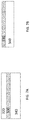
- FIG. 1 depicts one embodiment where 100 represents a substrate upon which the thermally conductive elements 200 , are affixed.
- FIG. 2 depicts the substrate 100 and thermally conductive elements 200 from FIG. 1 with the addition of a thermally active adhesion layer, 300 .
- FIG. 3 shows one embodiment of the invention, wherein an individual component 500 is released from the substrate along with the thermally conductive element 210 affixed to component 500 .
- FIG. 4 illustrates an additional side view of the embodiment of FIG. 3 .
- FIG. 5 illustrates an embodiment wherein the component 510 is attached directly to the thermally active adhesion layer 300 , with the thermally conductive element being permanently affixed to the substrate and having an thermally active adhesion layer on the opposite surface, such that only the component 510 is released.
- FIG. 6 illustrates an embodiment wherein the thermally conductive elements 200 are incorporated into the thermally active adhesion layer 300 .
- FIGS. 7A-B illustrate side views of single and double sided thermally active adhesion layer 300 .
- processing refers to the action and/or processes of a computer or computing system, or similar electronic data center device, that manipulates and/or transforms data represented as physical quantities (e.g., electronic) within the computing system's registers and/or memories into other data similarly represented as physical quantities within the computing system's memories, registers or other such information storage, transmission, or viewing devices.
- physical quantities e.g., electronic
- embodiments of the present invention provide an approach for separating a selected component from a plurality of components in a multi-component medium.
- a multi-component medium is created, including thermally conductive layer into which a template of patterned thermally conductive elements that are thermally separated from each other, a thermally active adhesion layer in thermal communication with the thermally conductive template, and a set of components attached to the thermally active adhesion layer in substantially the same pattern as thermally conductive template.
- the medium allows a selected component to be released by applying energy to a selected thermally conductive element corresponding to the selected component, causing a temperature change reducing the adhesion of the thermally active adhesion layer, without releasing non-selected components.
- solutions disclosed herein include methods and materials that can utilize any energy source, including but not limited to convection, radiation, and conduction, along with a shaped thermally conductive region to customize the temperature profile in ways unattainable using prior conventional methodologies. This becomes particularly important in transferring single electronic components from donor to receiver substrates.
- Heat spreaders have been used for thousands of years in metal cookware and other applications to get an even temperature distribution across a surface. Modern applications sometimes include use of them in thermal control of high-density electronics, control of temperature profiles in photovoltaic systems, and a myriad of other applications. Heat spreaders are typically based on materials that have high thermal conductivity and are used to reduce the peak temperature by spreading the heat across a broad area. Obviously, heat flows via conduction from high temperature to low temperature in these thermal spreading applications. Heat pipes and other more complicated systems can be used as well, depending on application, for thermal control. The fundamental properties of thermodynamics come into play and there are conductive, convective, and radiative energy transport mechanisms that all interact to create a time-dependent temperature profile across a surface.
- conduction is the passing of vibrational energy in which a lattice of atoms or molecules will oscillate and transfer vibrational energy across a material.
- Physicists model this vibrational energy transfer in terms of phonon transport. Packets of vibrational energy are treated as discrete phonons in several models. Materials of lower inherent thermal conductivity can slow the propagation of vibrational energy (or phonons) across a region. Controlling the temperature profile on a nano or micro scale is difficult because lattice vibrational energy naturally flows from high temperature to low temperature on a molecular/atomic scale.
- Thermal release tape is now commonly used in electronic manufacturing where the tape loses its adhesive strength upon reaching a threshold temperature. Tape manufacturers may use phase change materials, expanding materials, and the like to induce a dramatic change in the adhesive strength as the temperature of the thermally active adhesion layer increases over a threshold temperature. Electronic components are often stuck to the thermally active adhesion layer and upon heating, can be released from the thermally active adhesion layer. This typically happens in bulk, where a large area of the tape is heated and all the effected components are released at once. These tapes are available in rolls for all wafer mounting systems and hence thermal release tape is widely used in semiconductor package industry.
- Laser induced forward transfer is a widely used direct transfer technique used in printing, electronics, biotechnology industries, and others. Lasers with relatively low fluence are used for more sensitive materials like organics or biological materials.
- a spot-focused laser is typically used in LIFT applications that defines the resolution of the final transfer as well.
- a pulsed laser beam is used and the energy of the beam is the driving force that propels material from donor surface to acceptor. This is a robust method that is compatible with a variety of materials both solid and liquid. Inks of variable viscosities and particle sizes are compatible with the LIFT methodology.
- solid materials such as electronic components can be transferred from donor to acceptor surfaces. Companies like Uniqarta, Nitto, Philips, and others are developing dynamic release layers (DRL) that will propel individual components from donor to acceptor, typically based on a rapidly expanding thermally active adhesion layer when laser light is applied.
- DRL dynamic release layers
- DRL layers are designed to absorb the laser wavelength light and then propel the materials to the acceptor substrate.
- the accuracy and transfer efficiency is often controlled by the dynamics of the DRL.
- researchers are still trying to develop transfer systems including new types of DRLs that improve positioning for micro and mini sized electronic components. Often these transfer mechanisms have to be very reliable and very accurate, within 10 ⁇ m of the final location upon transfer to the acceptor substrate.
- Current methodologies and materials fall short of the accuracy and transfer efficiency goals for the electronics industry.
- a method that includes, for instance: using shaped thermally conductive materials such as pyrolytic graphite or other good conductor materials that define the release area for the electronic component and subsequently alter temperature with a laser to release it from thermal release tape.
- shaped thermally conductive materials such as pyrolytic graphite or other good conductor materials that define the release area for the electronic component and subsequently alter temperature with a laser to release it from thermal release tape.
- FIG. 1 illustrates an example of a substrate 100 and a set of patterned thermally conductive elements 200 in thermal communication with the substrate 100 .
- Thermally conductive elements 200 may be provided in a template defining the shape and area of the thermally conductive elements 200 . Note that the individual thermally conductive elements 200 are physically separated from each other to ensure that thermal conductivity, or the spreading of a thermal differential, including but not limited to heating or cooling, from a source, only occurs on individual elements, without conducting to adjacent elements. This concept applies generally to all embodiments described herein, allowing for site specific heat transference, and thus allowing for the individual release of devices.
- the shape and spacing of thermally conductive elements 200 are not meant to be limiting, as any array of shapes may be used depending on the end application.
- FIG. 2 illustrates, in one embodiment, the addition of a thermally active adhesion layer 300 in thermal communication a thermally conductive layer.
- This thermally conductive layer has been patterned to form a thermally conductive template that has a plurality of conductive elements 200 , with each thermally conductive element 200 being thermally separated from some or all other thermally conductive elements by a set of separators.
- the thermally conductive elements 200 may be physically separated. For instance, the thermally conductive material may be etched to ensure that there are gaps between each element. Alternatively, thermally conductive material may be placed physically onto a surface and manually inspected to ensure separation.
- Thermally active adhesion layer 300 is an interface between the thermally conductive template formed by thermally conductive elements 200 and the set of components that provides an attractive force between the conductive template and the components.
- thermally active adhesion layer 300 may be comprised of a thermally active adhesive, such as a multi-layer tape.
- a thermally active adhesive is the thermal release tapes produced by Nitto Denko Inc. REVALPHA product line, although it should be understood that a thermally active adhesive could include any adhesives known in the art or using any other solution now known or later discovered, including, but not limited to tape, resins, thin films, functional coatings, polymers such as PDMS and/or any other substance used for its ability to adhere.
- the attractive force in thermally active adhesion layer 300 can be attributed to forces of other types including, but not limited to, Van der Waals forces, electrostatic forces, magnetic forces, surface tension forces, tackiness, cohesion, which has an attractive force which can be altered when the temperature is altered.
- the separators between conductive elements 200 allow a temperature differential to be applied to an individual element 210 of thermally conductive elements 200 (e.g., such that individual element is heated, cooled, or otherwise thermally altered), without thermally altering other thermally conductive elements 200 on the thermally conductive template.
- the result is a temperature differential affecting 310 , which is the area of thermal active layer 300 that is impacted by the temperature change in 210 .
- a heat source including but not limited to a laser, applied to area 210 of substrate 100 , will activate only region 310 of thermally active adhesion layer 300 by virtue of the individual thermally conductive element 210 , without affecting other thermally conductive elements 200 , and thus other regions of thermally active adhesion layer 300 .
- a particular thermally conductive element 210 can spread the heat across a single portion 310 of the thermally active adhesion layer, allowing for the removal of a single area of interest.
- heat may be used, it is intended to include any thermal differential. For instance, heating, cooling, temperature gradients, or fluxes may all be utilized to activate the thermally active adhesion layer.
- the thermal differentiation may actually spread beyond the single portion 310 , activating multiple areas at once, but only within a threshold. Where the threshold for release is not met, the thermally active adhesion layer will not be activated to release the respective element. Alternatively, the thermal differentiation may not need to spread across the entire area or volume of the single portion 310 of the thermally active adhesion layer in order to reach a threshold for releasing the respective element.
- component 500 of a set of components is released without affecting any other components in the vicinity of other patterned thermally conductive elements.
- Component 500 can include any nano or micro scale electronic device for which binning, sorting, testing, or placing may be necessary including, but not limited to LEDs, micro LEDs, mini LEDS, photovoltaic devices, concentrator photovoltaic devices, transistors, capacitors, inductors, diodes, resistors, thermoelectrics, and a myriad of other microelectronic devices.
- the release may be performed by methods such as, including but not limited to, gravity alone, such that the force of gravity is stronger than the remaining force of the thermally active adhesion layer, and/or external forces e.g. vibrational, adhesion (via tape, elastomer stamp, static electricity, etc.), or magnetic forces that are applied to assist in the removal of the component 500 .
- FIG. 4 illustrates a side view of embodiments in this arrangement, wherein the thermally conductive element is released with the component.
- a substrate 400 may have a thermally active adhesion layer 300 applied thereon.
- the plurality of thermally conductive elements 200 are affixed to the thermally active adhesion layer 300 , and permanently affixed to components 500 , such that when heat is applied to a particular component 500 in the vicinity of thermally conductive element 210 , the individual component 500 is released due to the spread of heat to region 310 of thermally active adhesion layer 300 , causing the release by thermal application.
- thermally conductive element 210 still attached to the component 500 may be useful. This embodiment is not meant to be limiting. It is to be understood that while a single element 500 is illustrated, multiple elements 500 may be released either simultaneously or sequentially by targeting multiple thermally conductive elements 200 .
- a plurality of predetermined components may be released simultaneously using multiple heat sources, or rapidly using a moving heat source.
- a plurality of components may be selected, for instance, based on properties shared across some of the components, and all released together after applying heat source to each individual component desired to be removed.
- FIG. 5 illustrates another embodiment wherein the thermally conductive element is in thermal communication with the substrate 400 and the thermally active adhesion layer 300 is in thermal communication with the thermally conductive elements 200 , and the set of components 500 are attached to the thermally active adhesion layer 300 .
- the components 500 are separated from the thermally conductive elements 200 and released independently.
- the individual component 510 can be released directly without other material connected thereon.
- the component 510 may be released due to gravitational force alone if that force is greater than the residual adhesive force of thermally active adhesion layer 300 at region 310 following the heat activated features.
- component 510 can be removed using a tape, stamp, static electricity, or other attractive forces that are stronger than the residual adhesive strength on the thermal release tape.
- This tape, stamp, etc. may be placed proximate to or in contact with components 500 before, during, or after application of the heat source to collect released components 500 .
- Static, magnetic, diamagnetic, vibrational, ultrasonic, gravitational, or similar forces may collect released components, as well as direct contact.
- a plurality of components 500 may be released using a single, moving heat source, or a plurality of heat sources.
- a thermal differential is applied to substrate 400 , e.g., via a laser.
- the thermal differential is conducted throughout substrate 400 to thermally conductive components 200 strongest in the vicinity of applied thermal differentiation.
- Thermally conductive element 210 for instance, conducts the thermal differentiation to thermally active adhesion layer 300 , strongest at region 310 .
- Barriers e.g., separators
- gaps between thermal conductive elements 200 limit the conductivity of thermal differentiation.
- individual component 510 Upon exceeding a threshold of thermal differentiation large enough to delaminate or release thermally active adhesion layer 300 at region 310 , individual component 510 is released.
- adhesion force to individual component 510 is reduced such that gravity alone will remove component 510 , but in some embodiments an external force stronger than the remaining adhesion will allow for component 510 to release.
- thermally conductive elements 200 in all embodiments can include but are not limited to pyrolytic graphite (PG), graphene, mica, and many other stratified or layered materials which have axial and radial conduction properties that are anisotropic. These materials have advantages because the desired outcome is to have heat spread uniformly across the confines of the thermally conductive material that is used to define the shape of the component to be released.
- other materials may also be used as a thermally conductive element, including but not limited to strong conductors such as metals, semiconductors, composites, alloys, and laminate materials.
- Graphene for example, has very good lateral conductivity and when laminated with metals or metal composites that are typically good isotropic conductors, the resultant thermally conductive region will have desirable properties according to embodiments of the invention disclosed herein.
- gravitational force alone may not be strong enough to release components from the adhesive region 310 .
- external forces such as vibration, ultrasonic, magnetic induced repulsion or attraction, adhesion from tapes, stamps, or static electricity or other methods can be used to release the component from the residual thermally active adhesion layer.
- FIG. 6 shows another embodiment where the thermally conductive elements are incorporated into thermal release tape directly.
- thermally conductive elements 200 are incorporated into the tape itself.
- element 210 is heated, the temperature spreads across the surface. This will change the adhesive strength in region 310 of the broader thermal release layer 300 .
- FIGS. 7A-B illustrate a more detailed view of thermally active adhesion layer 300 .
- FIG. 7A illustrates a double sided thermally active adhesion layer 300 including a pressure sensitive thermally active adhesion layer 320 , a backing layer 330 , and a thermal release adhesive 340 .
- pressure sensitive adhesive 320 is applied to the thermally conductive element 200 or substrate 400 , allowing component 500 to be released upon activation of the thermal release adhesive 340 losing adhesion properties.
- FIG. 7B a single sided thermally active adhesion layer 300 is illustrated, having only backing layer 330 and thermal release adhesive 340 .
- a single type of component 500 may be included.
- a mixture of component types 500 can be utilized, afforded by the methods disclosed herein, via release of particular components desired or the release of non-contiguous LEDs, for example, from a wafer.
- a combination of macro and micro components may be utilized due to the strict control afforded.
- thermally conductive elements may be etched (e.g., via laser, oxygen plasma, etc.) using a mask to ensure that there are gaps between each thermally conductive element.
- thermally conductive material could be physically placed (e.g., deposited) onto a surface and the surface inspected to be sure the thermally conductive elements corresponding to individual components are not in contact with one another.
- stealth diced components have the smallest kerf spacing between the components and this can be enlarged via stretching on a hoop, as should be understood to one of ordinary skill in the art.
- Other dicing techniques like laser ablation can also be used to singulate the components on the wafer and this dicing technique also results in a gap between the individual components.
Abstract
Description
Claims (7)
Priority Applications (2)
| Application Number | Priority Date | Filing Date | Title |
|---|---|---|---|
| US16/870,327 US11214015B2 (en) | 2019-08-23 | 2020-05-08 | Methods and systems for controlling temperature across a region defined by using thermally conductive elements |
| PCT/US2020/047157 WO2021041142A1 (en) | 2019-08-23 | 2020-08-20 | Methods and systems for controlling temperature across a region defined by using thermally conductive elements |
Applications Claiming Priority (2)
| Application Number | Priority Date | Filing Date | Title |
|---|---|---|---|
| US201962890735P | 2019-08-23 | 2019-08-23 | |
| US16/870,327 US11214015B2 (en) | 2019-08-23 | 2020-05-08 | Methods and systems for controlling temperature across a region defined by using thermally conductive elements |
Publications (2)
| Publication Number | Publication Date |
|---|---|
| US20210053297A1 US20210053297A1 (en) | 2021-02-25 |
| US11214015B2 true US11214015B2 (en) | 2022-01-04 |
Family
ID=74646664
Family Applications (1)
| Application Number | Title | Priority Date | Filing Date |
|---|---|---|---|
| US16/870,327 Active US11214015B2 (en) | 2019-08-23 | 2020-05-08 | Methods and systems for controlling temperature across a region defined by using thermally conductive elements |
Country Status (2)
| Country | Link |
|---|---|
| US (1) | US11214015B2 (en) |
| WO (1) | WO2021041142A1 (en) |
Citations (8)
| Publication number | Priority date | Publication date | Assignee | Title |
|---|---|---|---|---|
| US5637169A (en) | 1990-09-27 | 1997-06-10 | 3D Systems, Inc. | Method of building three dimensional objects with sheets |
| US20060124241A1 (en) * | 2004-12-09 | 2006-06-15 | Nitto Denko Corporation | Method of thermal adherend release and apparatus for thermal adherend release |
| US8012566B2 (en) | 2006-07-12 | 2011-09-06 | Hewlett-Packard Development Company, L.P. | Microneedles formed by electroplating and selectively releasing temperature sensitive layers |
| WO2012142177A2 (en) | 2011-04-11 | 2012-10-18 | Ndsu Research Foundation | Selective laser-assisted transfer of discrete components |
| US20130228221A1 (en) | 2011-08-05 | 2013-09-05 | Solexel, Inc. | Manufacturing methods and structures for large-area thin-film solar cells and other semiconductor devices |
| US8661655B2 (en) | 2002-05-24 | 2014-03-04 | Koninklijke Philips N.V. | Method suitable for transferring a component supported by a carrier to a desired position on a substrate, and a device designed for this |
| US20180261570A1 (en) | 2017-03-13 | 2018-09-13 | SelfArray, Inc. | Methods and systems for parallel assembly, transfer, and bonding of ferromagnetic components |
| US20190015873A1 (en) | 2017-07-12 | 2019-01-17 | SelfArray, Inc. | Methods and systems for sorting a plurality of components for directed self-assembly |
-
2020
- 2020-05-08 US US16/870,327 patent/US11214015B2/en active Active
- 2020-08-20 WO PCT/US2020/047157 patent/WO2021041142A1/en active Application Filing
Patent Citations (9)
| Publication number | Priority date | Publication date | Assignee | Title |
|---|---|---|---|---|
| US5637169A (en) | 1990-09-27 | 1997-06-10 | 3D Systems, Inc. | Method of building three dimensional objects with sheets |
| US8661655B2 (en) | 2002-05-24 | 2014-03-04 | Koninklijke Philips N.V. | Method suitable for transferring a component supported by a carrier to a desired position on a substrate, and a device designed for this |
| US20060124241A1 (en) * | 2004-12-09 | 2006-06-15 | Nitto Denko Corporation | Method of thermal adherend release and apparatus for thermal adherend release |
| US8012566B2 (en) | 2006-07-12 | 2011-09-06 | Hewlett-Packard Development Company, L.P. | Microneedles formed by electroplating and selectively releasing temperature sensitive layers |
| WO2012142177A2 (en) | 2011-04-11 | 2012-10-18 | Ndsu Research Foundation | Selective laser-assisted transfer of discrete components |
| US9862141B2 (en) | 2011-04-11 | 2018-01-09 | Ndsu Research Foundation | Selective laser-assisted transfer of discrete components |
| US20130228221A1 (en) | 2011-08-05 | 2013-09-05 | Solexel, Inc. | Manufacturing methods and structures for large-area thin-film solar cells and other semiconductor devices |
| US20180261570A1 (en) | 2017-03-13 | 2018-09-13 | SelfArray, Inc. | Methods and systems for parallel assembly, transfer, and bonding of ferromagnetic components |
| US20190015873A1 (en) | 2017-07-12 | 2019-01-17 | SelfArray, Inc. | Methods and systems for sorting a plurality of components for directed self-assembly |
Non-Patent Citations (1)
| Title |
|---|
| Young, Lee, Application No. PCT/US2020/47157, Search Report & Written Opinion, dated Nov. 19, 2020, 15 pgs. |
Also Published As
| Publication number | Publication date |
|---|---|
| US20210053297A1 (en) | 2021-02-25 |
| WO2021041142A1 (en) | 2021-03-04 |
Similar Documents
| Publication | Publication Date | Title |
|---|---|---|
| Wang et al. | Hybrid magnetic micropillar arrays for programmable actuation | |
| US20170210117A1 (en) | Non-Contact Transfer Printing | |
| Nie et al. | Long distance transport of microdroplets and precise microfluidic patterning based on triboelectric nanogenerator | |
| US20180169942A1 (en) | Apparatus and method for release of additively manufactured products and build platform | |
| Mastrangeli et al. | Challenges for capillary self-assembly of microsystems | |
| Luo et al. | Thermal controlled tunable adhesive for deterministic assembly by transfer printing | |
| Hsu et al. | Diamagnetically levitated milli-robots for heterogeneous 3D assembly | |
| Kim et al. | Ultimate control of rate-dependent adhesion for reversible transfer process via a thin elastomeric layer | |
| Reis et al. | Toward enhancement of water vapour condensation using wettability gradient surface | |
| JP7177852B2 (en) | Methods for stamping and embossing | |
| Chang et al. | Self-transport and self-alignment of microchips using microscopic rain | |
| Ivanova et al. | Removal of micrometer size particles from surfaces using laser-induced thermocapillary flow: Experimental results | |
| Liu et al. | Sacrificial layer-assisted nanoscale transfer printing | |
| Fan et al. | Low-cost silicon wafer dicing using a craft cutter | |
| US11214015B2 (en) | Methods and systems for controlling temperature across a region defined by using thermally conductive elements | |
| WO2004093171A1 (en) | Pattern forming apparatus and pattern forming method | |
| Wang et al. | Enhancing spontaneous droplet motion on structured surfaces with tailored wedge design | |
| Dodd et al. | Planar selective Leidenfrost propulsion without physically structured substrates or walls | |
| Bindiganavale et al. | Demonstration of hotspot cooling using digital microfluidic device | |
| Darmawan et al. | Deposition of poly (3, 4-ethylenedioxythiophene)–poly (styrenesulfonate)(PEDOT-PSS) particles using standing surface acoustic waves and electrostatic deposition method for the rapid fabrication of transparent conductive film | |
| Kuran et al. | Integration of laser die transfer and magnetic self-assembly for ultra-thin chip placement | |
| Wang et al. | Programmable micro-transfer-printing for heterogeneous material integration | |
| US20060105549A1 (en) | Manipulation of micrometer-sized electronic objects with liquid droplets | |
| Fan et al. | Micro-scale droplet deposition for micro-object self-alignment release based on water condensation | |
| KR20150056500A (en) | Method and device for embossing |
Legal Events
| Date | Code | Title | Description |
|---|---|---|---|
| AS | Assignment |
Owner name: SELFARRAY, INC., NEW YORK Free format text: ASSIGNMENT OF ASSIGNORS INTEREST;ASSIGNORS:BALLINGER, CLINTON;CONWARD, MICHAEL;WANG, PEI-I;REEL/FRAME:052613/0204 Effective date: 20200501 |
|
| FEPP | Fee payment procedure |
Free format text: ENTITY STATUS SET TO UNDISCOUNTED (ORIGINAL EVENT CODE: BIG.); ENTITY STATUS OF PATENT OWNER: SMALL ENTITY |
|
| FEPP | Fee payment procedure |
Free format text: ENTITY STATUS SET TO SMALL (ORIGINAL EVENT CODE: SMAL); ENTITY STATUS OF PATENT OWNER: SMALL ENTITY |
|
| STPP | Information on status: patent application and granting procedure in general |
Free format text: DOCKETED NEW CASE - READY FOR EXAMINATION |
|
| STPP | Information on status: patent application and granting procedure in general |
Free format text: NON FINAL ACTION MAILED |
|
| STPP | Information on status: patent application and granting procedure in general |
Free format text: RESPONSE TO NON-FINAL OFFICE ACTION ENTERED AND FORWARDED TO EXAMINER |
|
| STPP | Information on status: patent application and granting procedure in general |
Free format text: NOTICE OF ALLOWANCE MAILED -- APPLICATION RECEIVED IN OFFICE OF PUBLICATIONS |
|
| STPP | Information on status: patent application and granting procedure in general |
Free format text: PUBLICATIONS -- ISSUE FEE PAYMENT VERIFIED |
|
| STCF | Information on status: patent grant |
Free format text: PATENTED CASE |