US11211448B2 - Capacitor structure with MIM layer over metal pillars - Google Patents
Capacitor structure with MIM layer over metal pillars Download PDFInfo
- Publication number
- US11211448B2 US11211448B2 US16/704,180 US201916704180A US11211448B2 US 11211448 B2 US11211448 B2 US 11211448B2 US 201916704180 A US201916704180 A US 201916704180A US 11211448 B2 US11211448 B2 US 11211448B2
- Authority
- US
- United States
- Prior art keywords
- metal
- capacitor
- layer
- over
- metal layer
- Prior art date
- Legal status (The legal status is an assumption and is not a legal conclusion. Google has not performed a legal analysis and makes no representation as to the accuracy of the status listed.)
- Active, expires
Links
Images


Classifications
-
- H01L28/91—
-
- H—ELECTRICITY
- H10—SEMICONDUCTOR DEVICES; ELECTRIC SOLID-STATE DEVICES NOT OTHERWISE PROVIDED FOR
- H10D—INORGANIC ELECTRIC SEMICONDUCTOR DEVICES
- H10D1/00—Resistors, capacitors or inductors
- H10D1/01—Manufacture or treatment
- H10D1/041—Manufacture or treatment of capacitors having no potential barriers
- H10D1/042—Manufacture or treatment of capacitors having no potential barriers using deposition processes to form electrode extensions
-
- H01L21/76885—
-
- H01L23/5223—
-
- H—ELECTRICITY
- H10—SEMICONDUCTOR DEVICES; ELECTRIC SOLID-STATE DEVICES NOT OTHERWISE PROVIDED FOR
- H10D—INORGANIC ELECTRIC SEMICONDUCTOR DEVICES
- H10D1/00—Resistors, capacitors or inductors
- H10D1/60—Capacitors
- H10D1/68—Capacitors having no potential barriers
- H10D1/692—Electrodes
- H10D1/711—Electrodes having non-planar surfaces, e.g. formed by texturisation
- H10D1/716—Electrodes having non-planar surfaces, e.g. formed by texturisation having vertical extensions
-
- H—ELECTRICITY
- H10—SEMICONDUCTOR DEVICES; ELECTRIC SOLID-STATE DEVICES NOT OTHERWISE PROVIDED FOR
- H10W—GENERIC PACKAGES, INTERCONNECTIONS, CONNECTORS OR OTHER CONSTRUCTIONAL DETAILS OF DEVICES COVERED BY CLASS H10
- H10W20/00—Interconnections in chips, wafers or substrates
- H10W20/01—Manufacture or treatment
- H10W20/031—Manufacture or treatment of conductive parts of the interconnections
- H10W20/063—Manufacture or treatment of conductive parts of the interconnections by forming conductive members before forming protective insulating material
-
- H—ELECTRICITY
- H10—SEMICONDUCTOR DEVICES; ELECTRIC SOLID-STATE DEVICES NOT OTHERWISE PROVIDED FOR
- H10W—GENERIC PACKAGES, INTERCONNECTIONS, CONNECTORS OR OTHER CONSTRUCTIONAL DETAILS OF DEVICES COVERED BY CLASS H10
- H10W20/00—Interconnections in chips, wafers or substrates
- H10W20/40—Interconnections external to wafers or substrates, e.g. back-end-of-line [BEOL] metallisations or vias connecting to gate electrodes
- H10W20/495—Capacitive arrangements or effects of, or between wiring layers
- H10W20/496—Capacitor integral with wiring layers
-
- H01L28/55—
-
- H—ELECTRICITY
- H10—SEMICONDUCTOR DEVICES; ELECTRIC SOLID-STATE DEVICES NOT OTHERWISE PROVIDED FOR
- H10D—INORGANIC ELECTRIC SEMICONDUCTOR DEVICES
- H10D1/00—Resistors, capacitors or inductors
- H10D1/60—Capacitors
- H10D1/68—Capacitors having no potential barriers
- H10D1/682—Capacitors having no potential barriers having dielectrics comprising perovskite structures
Definitions
- the present disclosure relates to integrated circuit (IC) fabrication, and more specifically, to a capacitor structure with metal pillars over which a metal-insulator-metal (MIM) layer undulates to create a higher density MIM capacitor.
- IC integrated circuit
- MIM metal-insulator-metal
- Capacitors are used widely in integrated circuits, such as accelerated processing units (APU) or graphics processing units (GPU), to store a charge. Capacitors can take a variety of forms such as vertical natural capacitors (VNCAP) and metal-oxide-metal (MOM) capacitors. Current capacitors are also formed from a combination of metal-insulator-metal (MIM) layers. MIM layers are typically arranged in a planar fashion in the IC, and electrical contacts are made to each of the metal layers to form the capacitor. Planar MIM capacitors use a relatively large area due to their planar layout. Consequently, the density of planar MIM capacitors and the capacitance per unit semiconductor area for planar MIM capacitors are not competitive. One approach to improve capacitance uses undulating MIM layers with contacts to ends of the layer, but this provides poor contact resistance. Finger-based MIM capacitors employ complex finger elements, but are more difficult to manufacture.
- a first aspect of the disclosure is directed to a capacitor structure for an integrated circuit (IC), the capacitor structure comprising: a plurality of spaced metal pillars, each metal pillar positioned on a corresponding underlying metal wire of an underlying metal layer; and a metal-insulator-metal layer over and between the plurality of spaced metal pillars.
- IC integrated circuit
- a second aspect of the disclosure includes a capacitor structure for an integrated circuit (IC), the capacitor structure comprising: a first metal pillar over a first underlying metal wire of an underlying metal layer; a second metal pillar over a second underlying metal wire of the underlying metal layer, the first metal pillar and the first underlying metal wire spaced from the second metal pillar and the second underlying metal wire; and a metal-insulator-metal layer over and between the first metal pillar and the second pillar, wherein the metal-insulator-metal layer includes a first capacitor metal layer over and between the first and second metal pillars, an insulator layer over the first capacitor metal layer, a second capacitor metal layer over the insulator layer; and at least one contact operatively coupled to the second capacitor metal layer.
- IC integrated circuit
- a third aspect of the disclosure related to a method of forming a metal-insulator-metal (MIM) capacitor for an integrated circuit, the method comprising: forming a metal pillar over each of a selected plurality of spaced underlying metal wires of an underlying metal layer; and forming a metal-insulator-metal layer over and between the metal pillars to form the MIM capacitor.
- MIM metal-insulator-metal
- FIG. 1 shows a cross-sectional view of forming cavities in a material layer over metal wires, according to embodiments of the disclosure.
- FIG. 2 shows a cross-sectional view of filling the cavities with a metal to form metal pillars, according to embodiments of the disclosure.
- FIG. 3 shows a cross-sectional view of removing the material layer to expose upper portions of the metal pillars over the metal wires, according to embodiments of the disclosure.
- FIG. 4 shows a cross-sectional view of forming a metal-insulator-metal (MIM) layer over the metal pillars to form a capacitor structure, according to embodiments of the disclosure.
- MIM metal-insulator-metal
- FIG. 5 shows a cross-sectional view of forming an interlayer dielectric over the capacitor structure, according to embodiments of the disclosure.
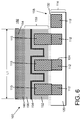
- FIG. 6 shows a cross-sectional view of patterning the capacitor structure, according to embodiments of the disclosure.
- FIG. 7 shows a cross-sectional view of forming contacts to the capacitor structure, according to embodiments of the disclosure.
- FIG. 8 shows a cross-sectional view of a capacitor structure in which the spacing between the metal pillar is non-uniform, according to another embodiment of the disclosure.
- Embodiments of the disclosure provide a capacitor structure for an integrated circuit (IC).
- the capacitor structure includes a plurality of spaced metal pillars with each metal pillar positioned on a corresponding underlying metal wire of an underlying metal layer.
- a metal-insulator-metal (MIM) layer is positioned over and between the metal pillars. At least one contact may be operatively coupled to an upper capacitor metal layer.
- the MIM layer creates a MIM capacitor that undulates over the metal pillars, creating a higher density capacitance compared to conventional planar MIM capacitors.
- the metal pillars extend into the MIM layer, which reduces contact resistance.
- the capacitor structure can be integrated into an IC with no major integration issues. A related method is also provided.
- FIGS. 1-7 embodiments of a method of forming a capacitor structure 100 ( FIG. 7 ), namely a MIM capacitor, for an integrated circuit (IC) 102 , are illustrated.
- FIGS. 1-3 show cross-sectional views of forming a metal pillar 110 ( FIG. 3 ) over each of a selected plurality of spaced underlying metal wires 112 of an underlying metal layer 114 .
- Underlying metal layer 114 may include any metal layer in IC 102 .
- underlying metal layer 114 may be a first metal layer, i.e., over a device layer (not shown).
- underlying metal layer 114 may be any back end of line (BEOL) layer.
- BEOL back end of line
- a BEOL layer is any layer formed on the semiconductor wafer (not shown) in the course of device manufacturing following first metallization.
- Underlying metal layer 114 may include any interlayer dielectric (ILD) 120 .
- ILD interlayer dielectric
- ILD 120 may include but is not limited to: carbon-doped silicon dioxide materials; fluorinated silicate glass (FSG); organic polymeric thermoset materials; silicon oxycarbide; SiCOH dielectrics; fluorine doped silicon oxide; spin-on glasses; silsesquioxanes, including hydrogen silsesquioxane (HSQ), methyl silsesquioxane (MSQ) and mixtures or copolymers of HSQ and MSQ; benzocyclobutene (BCB)-based polymer dielectrics, and any silicon-containing low-k dielectric.
- FSG fluorinated silicate glass
- organic polymeric thermoset materials silicon oxycarbide
- SiCOH dielectrics fluorine doped silicon oxide
- spin-on glasses silsesquioxanes, including hydrogen silsesquioxane (HSQ), methyl silsesquioxane (MSQ) and mixtures or copolymers of HSQ and MSQ
- BCB benzocyclo
- spin-on low-k films with SiCOH-type composition using silsesquioxane chemistry examples include HOSPTM (available from Honeywell), JSR 5109 and 5108 (available from Japan Synthetic Rubber), ZirkonTM (available from Shipley Microelectronics, a division of Rohm and Haas), and porous low-k (ELk) materials (available from Applied Materials).
- HOSPTM available from Honeywell
- JSR 5109 and 5108 available from Japan Synthetic Rubber
- ZirkonTM available from Shipley Microelectronics, a division of Rohm and Haas
- porous low-k (ELk) materials available from Applied Materials
- carbon-doped silicon dioxide materials, or organosilanes examples include Black DiamondTM (available from Applied Materials) and CoralTM (available from Lam Research).
- An example of an HSQ material is FOxTM (available from Dow Corning).
- Metal wires 112 in underlying metal layer 114 may be formed in any now known or later developed fashion.
- metal wires 112 may be formed by lithographically defining openings 124 in ILD 120 , then depositing metal to fill resulting trenches, and then removing excess metal, e.g., by means of chemical-mechanical polishing (planarization). Openings 124 may be etched in ILD 120 , i.e., using a mask (not shown). Etching generally refers to the removal of material from a substrate (or structures formed on the substrate), and is often performed with a mask in place so that material may selectively be removed from certain areas of the substrate, while leaving the material unaffected, in other areas of the substrate.
- etching There are generally two categories of etching, (i) wet etch and (ii) dry etch.
- Wet etch is performed with a solvent (such as an acid) which may be chosen for its ability to selectively dissolve a given material (such as oxide), while, leaving another material (such as polysilicon) relatively intact.
- a wet etch will generally etch a homogeneous material (e.g., oxide) isotropically, but a wet etch may also etch single-crystal materials (e.g. silicon wafers) anisotropically.
- Dry etch may be performed using a plasma. Plasma systems can operate in several modes by adjusting the parameters of the plasma.
- etching produces energetic free radicals, neutrally charged, that react at the surface of the wafer. Since neutral particles attack the wafer from all angles, this process is isotropic. Ion milling, or sputter etching, bombards the wafer with energetic ions of noble gases which approach the wafer approximately from one direction, and therefore this process is highly anisotropic.
- Reactive-ion etching RIE operates under conditions intermediate between sputter and plasma etching and may be used to produce deep, narrow features, such as STI trenches. Openings 124 for metal wires 112 may be etched, for example, using RIE.
- Depositing may include any now known or later developed techniques appropriate for the material to be deposited including but are not limited to, for example: chemical vapor deposition (CVD), low-pressure CVD (LPCVD), plasma-enhanced CVD (PECVD), semi-atmosphere CVD (SACVD) and high density plasma CVD (HDPCVD), rapid thermal CVD (RTCVD), ultra-high vacuum CVD (UHVCVD), limited reaction processing CVD (LRPCVD), metalorganic CVD (MOCVD), sputtering deposition, ion beam deposition, electron beam deposition, laser assisted deposition, thermal oxidation, thermal nitridation, spin-on methods, physical vapor deposition (PVD), atomic layer deposition (ALD), chemical oxidation, molecular beam epitaxy (MBE), plating, evaporation.
- CVD chemical vapor deposition
- LPCVD low-pressure CVD
- PECVD plasma-enhanced CVD
- SACVD semi
- metal may be deposited using, for example, ALD.
- a refractory metal liner (not shown) of, for example, ruthenium (Ru), tantalum (Ta), titanium (Ti), tungsten (W), iridium (Jr), rhodium (Rh), platinum (Pt), etc., or mixtures of thereof, may be deposited prior to metal deposition.
- Metal wires 112 may include any conductor employed in IC wiring, for example, copper. While three metal wires 112 are shown in the drawing, two or more than three may be employed. The number of metal wires 112 may be chosen to create a certain size capacitor structure, as will be described. As will be described, metal wires (not shown in FIG. 1 ) may also be formed for underlying metal layer 114 in a non-MIM region 158 ( FIGS. 4-7 ), e.g., for logic, adjacent to the MIM capacitor.
- FIG. 1 also shows forming a material layer 130 over an etch stop layer (ESL) 132 over selected plurality of spaced underlying metal wires 112 . That is, material layer 130 and etch stop layer (ESL) 132 are formed over underlying metal layer 114 .
- ESL 132 may include any material typically used to stop etching such as but not limited to silicon nitride (e.g., n-Blok), and may be formed by any appropriate deposition technique, e.g., CVD.
- Material layer 130 is formed over ESL 132 , e.g., by CVD.
- Material layer 130 may include any sacrificial material capable of defining cavities for metal pillar 110 ( FIG. 3 ) formation.
- material layer 130 may include any ILD material listed herein.
- FIG. 1 also shows patterning a cavity 140 in material layer 130 and ESL 132 over each of selected plurality of spaced underlying metal wires 112 .
- Cavities 140 may be patterned by forming a mask (not shown), patterning the mask and etching to remove material layer 130 and ESL 132 over underlying metal wires 112 .
- the etching may include, for example, a RIE. While shown with each cavity 140 aligned over metal wires 112 , some misalignment may be allowed.
- a cavity 140 is not necessarily required over each metal wire 112 , a cavity 140 is not necessarily required over each metal wire, e.g., where more than two metal wires 112 are provided between outermost metal wires.
- the number of cavities 140 (and hence the number of metal pillars 110 formed therein) may be defined to customize the number of undulations in an eventually formed MIM layer, and hence, used to control the capacitance of capacitor structure 100 ( FIG. 7 ), i.e., by controlling its length created in the undulations.
- at least three metal wires 112 and at least three metal pillars 110 are provided.
- FIG. 2 shows a cross-sectional view of filling each cavity 140 with a metal 142 .
- Metal 142 may be deposited, e.g., by ALD, followed by a planarization step to remove excess metal.
- Metal 142 may be the same as or different than metal wires 112 .
- metal 142 may include copper (Cu).
- metal 142 may include but is not limited to: titanium, titanium nitride, ruthenium, tungsten, cobalt or any other conductive metal.
- FIG. 3 shows a cross-sectional view of removing material layer 130 to leave a metal pillar 110 over each of selected plurality of spaced underlying metal wires 112 . An upper portion of metal pillars 110 are exposed by this process.
- Material layer 130 may be removed using any appropriate etching process selective to metal 142 ( FIG. 2 ), e.g., a RIE.
- Metal pillars 110 are spaced apart per the spacing of underlying metal wires 112 .
- FIGS. 4-7 show cross-sectional views of forming a metal-insulator-metal (MIM) layer 150 over and between spaced metal pillars 110 to form capacitor structure 100 ( FIG. 7 ).
- Forming MIM layer 150 over and between spaced metal pillars 110 includes forming a first capacitor metal layer 152 over and between metal pillars 110 , forming an insulator layer 154 over first capacitor metal layer 152 , and forming a second capacitor metal layer 156 over insulator layer 154 .
- Each layer 152 , 154 , 156 may be formed by any appropriate deposition for the materials used, e.g., ALD. As illustrated in FIG.
- each metal pillar 110 is contacted on three sides by first capacitor metal layer 152 , which improves a contact resistance of metal wire 112 to first capacitor metal layer 152 that provides a first electrode of capacitor structure 100 ( FIG. 7 ).
- Capacitor metal layers 152 , 156 may include any now known or later developed capacitor electrode material including but not limited to: titanium nitride (TiN), ruthenium (Ru), tantalum nitride (TaN), or any other conductive materials.
- Insulator layer 154 may include any now known or later developed high dielectric constant (high-K) material appropriate for a MIM capacitor.
- insulator layer 154 may include but is not limited to: tantalum oxide (Ta 2 O 5 ), barium titanium oxide (BaTiO 3 ), hafnium oxide (HfO 2 ), zirconium oxide (ZrO 2 ), aluminum oxide (Al 2 O 3 ), hafnium silicate oxide (HfSixOy) or hafnium silicon oxynitride (HfSixOyNz), where x, y, and z represent relative proportions, each greater than or equal to zero.
- spacing between metal pillars 110 may be such that first capacitor metal layer 152 and insulator layer 154 undulate over metal pillars 110 . That is, first capacitor metal layer 152 and insulator layer 154 extend in valleys between metal pillars 110 and peaks over metal pillars 110 , in a somewhat sinusoidal fashion. In this manner, the length of capacitor structure 100 ( FIG. 7 ) can be increased without increasing geographic area within IC 102 .
- second capacitor metal layer 156 may fill any remaining space between metal pillars 110 (e.g., left between insulator layer 154 as it passes over metal pillars 110 ). Second capacitor metal layer 156 also extends over metal pillars 110 .
- FIGS. 4-6 also show an additional metal wire 112 (right side) in underlying metal layer 114 in non-MIM (e.g., logic) region 158 that is not covered by a metal pillar 110 .
- embodiments of the method may further include forming an ILD 160 over capacitor structure 100 .
- ILD 160 may include any now known or later developed ILD such as listed herein relative to ILD 120 . Any necessary planarization may be carried out at this stage.
- FIG. 6 shows a cross-sectional view of patterning capacitor structure 100 to a selected dimension(s), e.g., trimming a length across page and/or depth into and out of page.
- Capacitor structure 100 may be patterned, for example, by patterning a mask 164 over capacitor structure 100 and etching to remove any un-desired MIM layer 150 .
- a length L 1 is shorter in FIG. 6 than a length L 2 in FIG. 5 .
- a depth of capacitor structure 100 into and out of the page could be similarly customized.
- dimension(s) of capacitor structure 100 can be customized to deliver the desired capacitance.
- Any MIM layer 150 that may be present in non-MIM region 158 of IC 102 can also be removed as part of the patterning of capacitor structure 100 .
- FIG. 7 shows a cross-sectional view of forming at least one contact 170 , 174 operatively coupled to second capacitor metal layer 156 . While one contact may be employed, at least two spaced contacts 170 , 174 operatively coupled to second capacitor metal layer 156 are advantageous to reduce contact resistance. Note, the embodiment shown in FIG. 7 also includes more than three metal pillar 110 and metal wire 112 pairs with MIM layer 150 thereover, and is longer than the FIG. 6 embodiment.
- the contact forming process may include replacing any ILD 160 removed during the patterning of FIG. 6 . ILD 160 may also be replaced over non-MIM region 158 , which is shown larger in FIG. 7 than in FIGS. 4-6 for clarity.
- Contact(s) 170 , 174 may be formed using any now known or later developed process.
- contact(s) 170 , 174 may be formed by lithographically defining openings 162 in ILD 160 , then depositing metal to fill resulting trenches, and then removing excess metal, e.g., by means of chemical-mechanical polishing (planarization). Openings 162 may be etched in ILD 160 , e.g., using RIE.
- the contact metal may be deposited using, for example, ALD.
- a refractory metal liner (not shown) of, for example, ruthenium (Ru), tantalum (Ta), titanium (Ti), tungsten (W), iridium (Jr), rhodium (Rh), platinum (Pt), etc., or mixtures of thereof, may be deposited prior to metal deposition.
- Contact(s) 170 , 174 may include any contact conductor employed in IC wiring, for example, copper. In one embodiment, contact 170 is aligned over a first metal pillar 110 A, and contact 174 is aligned over second metal pillar 110 B, but this is not necessary in all instances. A number of contacts 170 , 174 may be customized to reduce contact resistance. As illustrated, metal wires, and/or contacts 176 for non-MIM region 158 may be formed with contact(s) 170 , 174 .
- FIG. 8 shows a cross-sectional view of another embodiment similar to FIG. 7 but in which the spacing between metal pillar 110 and metal wire 112 pairs is non-uniform.
- MIM layer 150 thus may have non-uniform length valleys and/or non-uniform length peaks.
- FIGS. 7 and 8 also show cross-sectional views of capacitor structure 100 for IC 102 , according to embodiments of the disclosure.
- Capacitor structure 100 may include a plurality of spaced metal pillars 110 with each metal pillar 110 positioned on a corresponding underlying metal wire 112 of underlying metal layer 114 .
- Metal wires 112 may include copper.
- ESL 132 may be adjacent a lower end of plurality of metal pillars 110 , i.e., over underlying metal layer 114 .
- Capacitor structure 100 also includes MIM layer 150 over and between plurality of spaced metal pillars 110 .
- MIM layer 150 includes first capacitor metal layer 152 over and between plurality of spaced metal pillars 110 , insulator layer 154 over first capacitor metal layer 152 , and second capacitor metal layer 156 over insulator layer 154 .
- the materials for capacitor metal layers 152 , 156 and insulator layer 154 may be as previously described.
- first capacitor metal layer 152 and insulator layer 154 undulate over spaced metal pillars 110 .
- first capacitor metal layer 152 and insulator layer 154 extend in valleys between metal pillars 110 and peaks over metal pillars 110 , in a somewhat sinusoidal fashion. As shown in the example in FIG.
- second capacitor metal layer 156 may fill any remaining space between metal pillars 110 , e.g., left between insulator layer 154 as it passes over metal pillars 110 . Second capacitor metal layer 156 extends over metal pillars 110 . MIM layer 150 thus forms capacitor structure 100 , i.e., a MIM capacitor. One or more metal pillars 110 may be positioned between the outermost metal pillars 110 A, 110 B ( FIG. 7 ), allowing customization of the length and thus capacitance value of MIM layer 150 and capacitor structure 100 .
- Capacitor structure 200 may also include at least one contact 170 , 174 operatively coupled to second capacitor metal layer 156 , i.e., a second electrode of capacitor structure 100 .
- Embodiments of the disclosure provide capacitor structure 100 that undulates over metal pillars 110 , creating a higher density capacitance compared to conventional planar MIM capacitors.
- Metal pillars 110 extend into MIM layer 150 with MIM layer on three sides of each pillar, which reduces contact resistance.
- capacitor structure 100 can be integrated into IC 102 with no major integration issues. Capacitor structure 100 is also compatible with decreasing dimensions of the latest technology nodes, e.g., 7 nanometers and beyond.
- the method as described above is used in the fabrication of integrated circuit chips.
- the resulting integrated circuit chips can be distributed by the fabricator in raw wafer form (that is, as a single wafer that has multiple unpackaged chips), as a bare die, or in a packaged form.
- the chip is mounted in a single chip package (such as a plastic carrier, with leads that are affixed to a motherboard or other higher level carrier) or in a multichip package (such as a ceramic carrier that has either or both surface interconnections or buried interconnections).
- the chip is then integrated with other chips, discrete circuit elements, and/or other signal processing devices as part of either (a) an intermediate product, such as a motherboard, or (b) an end product.
- the end product can be any product that includes integrated circuit chips, ranging from toys and other low-end applications to advanced computer products having a display, a keyboard or other input device, and a central processor.
- Approximating language may be applied to modify any quantitative representation that could permissibly vary without resulting in a change in the basic function to which it is related. Accordingly, a value modified by a term or terms, such as “about”, “approximately” and “substantially”, are not to be limited to the precise value specified. In at least some instances, the approximating language may correspond to the precision of an instrument for measuring the value.
- range limitations may be combined and/or interchanged, such ranges are identified and include all the sub-ranges contained therein unless context or language indicates otherwise. “Approximately” as applied to a particular value of a range applies to both values, and unless otherwise dependent on the precision of the instrument measuring the value, may indicate +/ ⁇ 10% of the stated value(s).
Landscapes
- Engineering & Computer Science (AREA)
- Power Engineering (AREA)
- Semiconductor Integrated Circuits (AREA)
Abstract
Description
Claims (20)
Priority Applications (1)
| Application Number | Priority Date | Filing Date | Title |
|---|---|---|---|
| US16/704,180 US11211448B2 (en) | 2019-12-05 | 2019-12-05 | Capacitor structure with MIM layer over metal pillars |
Applications Claiming Priority (1)
| Application Number | Priority Date | Filing Date | Title |
|---|---|---|---|
| US16/704,180 US11211448B2 (en) | 2019-12-05 | 2019-12-05 | Capacitor structure with MIM layer over metal pillars |
Publications (2)
| Publication Number | Publication Date |
|---|---|
| US20210175323A1 US20210175323A1 (en) | 2021-06-10 |
| US11211448B2 true US11211448B2 (en) | 2021-12-28 |
Family
ID=76210250
Family Applications (1)
| Application Number | Title | Priority Date | Filing Date |
|---|---|---|---|
| US16/704,180 Active 2040-04-07 US11211448B2 (en) | 2019-12-05 | 2019-12-05 | Capacitor structure with MIM layer over metal pillars |
Country Status (1)
| Country | Link |
|---|---|
| US (1) | US11211448B2 (en) |
Families Citing this family (2)
| Publication number | Priority date | Publication date | Assignee | Title |
|---|---|---|---|---|
| US12581943B2 (en) | 2021-09-21 | 2026-03-17 | Qualcomm Incorporated | Three-dimensional (3D) metal-insulator-metal capacitor (MIMCAP) including stacked vertical metal studs for increased capacitance density and related fabrication methods |
| US12034039B2 (en) | 2021-10-18 | 2024-07-09 | Globalfoundries Singapore Pte. Ltd. | Three electrode capacitor structure using spaced conductive pillars |
Citations (6)
| Publication number | Priority date | Publication date | Assignee | Title |
|---|---|---|---|---|
| US20050275005A1 (en) | 2004-06-11 | 2005-12-15 | Seung-Man Choi | Metal-insulator-metal (MIM) capacitor and method of fabricating the same |
| US20120304742A1 (en) | 2004-04-02 | 2012-12-06 | ChipSensors Limited | Integrated cmos porous sensor |
| US20130181326A1 (en) | 2012-01-18 | 2013-07-18 | International Business Machines Corporation | Multilayer mim capacitor |
| US20140225222A1 (en) * | 2013-02-11 | 2014-08-14 | Taiwan Semiconductor Manufacturing Company, Ltd. | Package with metal-insulator-metal capacitor and method of manufacturing the same |
| US20160000344A1 (en) | 2014-07-01 | 2016-01-07 | Ariel Cao | Hermetically sealed implant sensors with vertical stacking architecture |
| US20190051659A1 (en) * | 2017-08-10 | 2019-02-14 | Globalfoundries Inc. | Integrated circuit structure having vfet and embedded memory structure and method of forming same |
-
2019
- 2019-12-05 US US16/704,180 patent/US11211448B2/en active Active
Patent Citations (6)
| Publication number | Priority date | Publication date | Assignee | Title |
|---|---|---|---|---|
| US20120304742A1 (en) | 2004-04-02 | 2012-12-06 | ChipSensors Limited | Integrated cmos porous sensor |
| US20050275005A1 (en) | 2004-06-11 | 2005-12-15 | Seung-Man Choi | Metal-insulator-metal (MIM) capacitor and method of fabricating the same |
| US20130181326A1 (en) | 2012-01-18 | 2013-07-18 | International Business Machines Corporation | Multilayer mim capacitor |
| US20140225222A1 (en) * | 2013-02-11 | 2014-08-14 | Taiwan Semiconductor Manufacturing Company, Ltd. | Package with metal-insulator-metal capacitor and method of manufacturing the same |
| US20160000344A1 (en) | 2014-07-01 | 2016-01-07 | Ariel Cao | Hermetically sealed implant sensors with vertical stacking architecture |
| US20190051659A1 (en) * | 2017-08-10 | 2019-02-14 | Globalfoundries Inc. | Integrated circuit structure having vfet and embedded memory structure and method of forming same |
Also Published As
| Publication number | Publication date |
|---|---|
| US20210175323A1 (en) | 2021-06-10 |
Similar Documents
| Publication | Publication Date | Title |
|---|---|---|
| US10879112B2 (en) | Self-aligned via forming to conductive line and related wiring structure | |
| US10347528B1 (en) | Interconnect formation process using wire trench etch prior to via etch, and related interconnect | |
| US10312188B1 (en) | Interconnect structure with method of forming the same | |
| US11437312B2 (en) | High performance metal insulator metal capacitor | |
| US11107880B2 (en) | Capacitor structure for integrated circuit, and related methods | |
| US6338999B1 (en) | Method for forming metal capacitors with a damascene process | |
| US11114338B2 (en) | Fully aligned via in ground rule region | |
| US10109524B2 (en) | Recessing of liner and conductor for via formation | |
| US10998227B2 (en) | Metal insulator metal capacitor with extended capacitor plates | |
| US10062647B2 (en) | Interconnect structure having tungsten contact copper wiring | |
| US11211448B2 (en) | Capacitor structure with MIM layer over metal pillars | |
| US9806032B1 (en) | Integrated circuit structure with refractory metal alignment marker and methods of forming same | |
| US12034039B2 (en) | Three electrode capacitor structure using spaced conductive pillars | |
| US6504205B1 (en) | Metal capacitors with damascene structures | |
| US11348867B2 (en) | Capacitor structure for integrated circuit and related methods | |
| US11699650B2 (en) | Integrated circuit structure with capacitor electrodes in different ILD layers, and related methods | |
| US10833067B1 (en) | Metal resistor structure in at least one cavity in dielectric over TS contact and gate structure | |
| US10381432B2 (en) | Advanced metal insulator metal capacitor | |
| US12550723B2 (en) | Structure for capacitor having defect-preventing regions in metal electrode | |
| US11195761B2 (en) | IC structure with short channel gate structure having shorter gate height than long channel gate structure | |
| US10109706B1 (en) | Method of forming high performance vertical natural capacitor (VNCAP) | |
| CN114220767A (en) | Semiconductor structure, manufacturing method thereof and memory |
Legal Events
| Date | Code | Title | Description |
|---|---|---|---|
| AS | Assignment |
Owner name: GLOBALFOUNDRIES INC., CAYMAN ISLANDS Free format text: ASSIGNMENT OF ASSIGNORS INTEREST;ASSIGNORS:SINGH, SUNIL K.;RAMANATHAN, ESWAR;REEL/FRAME:051191/0796 Effective date: 20191205 |
|
| FEPP | Fee payment procedure |
Free format text: ENTITY STATUS SET TO UNDISCOUNTED (ORIGINAL EVENT CODE: BIG.); ENTITY STATUS OF PATENT OWNER: LARGE ENTITY |
|
| AS | Assignment |
Owner name: GLOBALFOUNDRIES U.S. INC., CALIFORNIA Free format text: ASSIGNMENT OF ASSIGNORS INTEREST;ASSIGNOR:GLOBALFOUNDRIES INC.;REEL/FRAME:054633/0001 Effective date: 20201022 |
|
| AS | Assignment |
Owner name: GLOBALFOUNDRIES U.S. INC., NEW YORK Free format text: RELEASE BY SECURED PARTY;ASSIGNOR:WILMINGTON TRUST, NATIONAL ASSOCIATION;REEL/FRAME:056987/0001 Effective date: 20201117 Owner name: GLOBALFOUNDRIES U.S. INC., NEW YORK Free format text: RELEASE OF SECURITY INTEREST;ASSIGNOR:WILMINGTON TRUST, NATIONAL ASSOCIATION;REEL/FRAME:056987/0001 Effective date: 20201117 |
|
| STPP | Information on status: patent application and granting procedure in general |
Free format text: NON FINAL ACTION MAILED |
|
| STPP | Information on status: patent application and granting procedure in general |
Free format text: RESPONSE TO NON-FINAL OFFICE ACTION ENTERED AND FORWARDED TO EXAMINER |
|
| STPP | Information on status: patent application and granting procedure in general |
Free format text: NOTICE OF ALLOWANCE MAILED -- APPLICATION RECEIVED IN OFFICE OF PUBLICATIONS |
|
| STPP | Information on status: patent application and granting procedure in general |
Free format text: PUBLICATIONS -- ISSUE FEE PAYMENT RECEIVED |
|
| STPP | Information on status: patent application and granting procedure in general |
Free format text: PUBLICATIONS -- ISSUE FEE PAYMENT VERIFIED |
|
| STCF | Information on status: patent grant |
Free format text: PATENTED CASE |
|
| MAFP | Maintenance fee payment |
Free format text: PAYMENT OF MAINTENANCE FEE, 4TH YEAR, LARGE ENTITY (ORIGINAL EVENT CODE: M1551); ENTITY STATUS OF PATENT OWNER: LARGE ENTITY Year of fee payment: 4 |