US11195440B2 - Display device and inspecting method therefor - Google Patents
Display device and inspecting method therefor Download PDFInfo
- Publication number
- US11195440B2 US11195440B2 US15/987,268 US201815987268A US11195440B2 US 11195440 B2 US11195440 B2 US 11195440B2 US 201815987268 A US201815987268 A US 201815987268A US 11195440 B2 US11195440 B2 US 11195440B2
- Authority
- US
- United States
- Prior art keywords
- resistance
- sensing wire
- sensing
- display area
- wire
- Prior art date
- Legal status (The legal status is an assumption and is not a legal conclusion. Google has not performed a legal analysis and makes no representation as to the accuracy of the status listed.)
- Active, expires
Links
Images


Classifications
-
- G—PHYSICS
- G09—EDUCATION; CRYPTOGRAPHY; DISPLAY; ADVERTISING; SEALS
- G09G—ARRANGEMENTS OR CIRCUITS FOR CONTROL OF INDICATING DEVICES USING STATIC MEANS TO PRESENT VARIABLE INFORMATION
- G09G3/00—Control arrangements or circuits, of interest only in connection with visual indicators other than cathode-ray tubes
- G09G3/006—Electronic inspection or testing of displays and display drivers, e.g. of LED or LCD displays
-
- G—PHYSICS
- G01—MEASURING; TESTING
- G01R—MEASURING ELECTRIC VARIABLES; MEASURING MAGNETIC VARIABLES
- G01R27/00—Arrangements for measuring resistance, reactance, impedance, or electric characteristics derived therefrom
- G01R27/02—Measuring real or complex resistance, reactance, impedance, or other two-pole characteristics derived therefrom, e.g. time constant
- G01R27/08—Measuring resistance by measuring both voltage and current
-
- G—PHYSICS
- G01—MEASURING; TESTING
- G01R—MEASURING ELECTRIC VARIABLES; MEASURING MAGNETIC VARIABLES
- G01R31/00—Arrangements for testing electric properties; Arrangements for locating electric faults; Arrangements for electrical testing characterised by what is being tested not provided for elsewhere
- G01R31/28—Testing of electronic circuits, e.g. by signal tracer
- G01R31/2801—Testing of printed circuits, backplanes, motherboards, hybrid circuits or carriers for multichip packages [MCP]
- G01R31/2818—Testing of printed circuits, backplanes, motherboards, hybrid circuits or carriers for multichip packages [MCP] using test structures on, or modifications of, the card under test, made for the purpose of testing, e.g. additional components or connectors
-
- G—PHYSICS
- G01—MEASURING; TESTING
- G01R—MEASURING ELECTRIC VARIABLES; MEASURING MAGNETIC VARIABLES
- G01R31/00—Arrangements for testing electric properties; Arrangements for locating electric faults; Arrangements for electrical testing characterised by what is being tested not provided for elsewhere
- G01R31/28—Testing of electronic circuits, e.g. by signal tracer
- G01R31/282—Testing of electronic circuits specially adapted for particular applications not provided for elsewhere
- G01R31/2825—Testing of electronic circuits specially adapted for particular applications not provided for elsewhere in household appliances or professional audio/video equipment
-
- G—PHYSICS
- G09—EDUCATION; CRYPTOGRAPHY; DISPLAY; ADVERTISING; SEALS
- G09G—ARRANGEMENTS OR CIRCUITS FOR CONTROL OF INDICATING DEVICES USING STATIC MEANS TO PRESENT VARIABLE INFORMATION
- G09G3/00—Control arrangements or circuits, of interest only in connection with visual indicators other than cathode-ray tubes
- G09G3/20—Control arrangements or circuits, of interest only in connection with visual indicators other than cathode-ray tubes for presentation of an assembly of a number of characters, e.g. a page, by composing the assembly by combination of individual elements arranged in a matrix no fixed position being assigned to or needed to be assigned to the individual characters or partial characters
-
- G—PHYSICS
- G09—EDUCATION; CRYPTOGRAPHY; DISPLAY; ADVERTISING; SEALS
- G09G—ARRANGEMENTS OR CIRCUITS FOR CONTROL OF INDICATING DEVICES USING STATIC MEANS TO PRESENT VARIABLE INFORMATION
- G09G2300/00—Aspects of the constitution of display devices
- G09G2300/04—Structural and physical details of display devices
- G09G2300/0421—Structural details of the set of electrodes
- G09G2300/0426—Layout of electrodes and connections
-
- G—PHYSICS
- G09—EDUCATION; CRYPTOGRAPHY; DISPLAY; ADVERTISING; SEALS
- G09G—ARRANGEMENTS OR CIRCUITS FOR CONTROL OF INDICATING DEVICES USING STATIC MEANS TO PRESENT VARIABLE INFORMATION
- G09G2330/00—Aspects of power supply; Aspects of display protection and defect management
- G09G2330/12—Test circuits or failure detection circuits included in a display system, as permanent part thereof
Definitions
- Exemplary embodiments of the present disclosure relate to a display device and a method of inspecting a display device for a defect.
- a display device such as a liquid crystal display (LCD) or an organic light emitting diode (OLED) display, includes a display panel including a plurality of pixels that display an image, and a plurality of signal lines. Each pixel may include a pixel electrode receiving a data signal. The pixel electrode may be connected to at least one transistor to receive the data signal.
- the display panel may include a plurality of stacked layers.
- a crack may be generated in a substrate or the stacked layers thereon.
- the crack may grow larger or spread to other layers or other regions over time, thereby causing a defect in the display panel.
- the signal lines e.g., in a data line or a scanning line
- the signal lines may become disconnected, a resistance may increase, or moisture may penetrate the display panel through the crack.
- a flexible display is a display that may be bent or warped while being manufactured and while being used. In this case, if a fine/micro crack exists in the substrate or the stacked layers of the display panel, even if there is no problem initially, the fine/micro crack may turn into a larger crack due to the warping or the bending of the display panel over time.
- Exemplary embodiments of the present disclosure provide a display device and a method of inspecting a display device for a defect in which the detection accuracy of the defect is increased.
- a display device includes a defect inspection circuit, and a display panel including a display area in which an image is displayed, and a peripheral area positioned outside the display area.
- the display panel includes at least one sensing wire positioned in the peripheral area and connected to the defect inspection circuit.
- the defect inspection circuit includes a resistance detection circuit that detects a resistance of the at least one sensing wire based on an output signal corresponding to the at least one sensing wire, a memory that stores first resistance information related to the resistance of the at least one sensing wire detected in a first inspection operation, and a comparator circuit including a first comparator that compares the first resistance information with second resistance information.
- the second resistance information is related to the resistance of the at least one sensing wire detected in a second inspection operation that is performed at a different time than the first inspection operation.
- the defect inspection circuit includes a pad portion that outputs a comparison result of the first comparator.
- the first resistance information and the second resistance information include a resistance value of the at least one sensing wire.
- the at least one sensing wire is one of a plurality of sensing wires
- the first resistance information and the second resistance information include a resistance comparison value between the plurality of sensing wires.
- the first resistance information and the second resistance information include a resistance value of the plurality of sensing wires.
- the comparator circuit further includes a second comparator that compares at least two resistances from among the plurality of sensing wires with each other to obtain the resistance comparison value.
- the plurality of sensing wires includes a first sensing wire and a second sensing wire positioned at a same side with respect to the display area.
- the plurality of sensing wires includes a first sensing wire and a second sensing wire positioned at opposite sides with respect to the display area.
- the plurality of sensing wires further includes a third sensing wire positioned at a same side with respect to the display area as the first sensing wire.
- At least one comparison result of the first comparator and the second comparator indicates a progress degree of a defect of the display device.
- the resistance detection circuit further includes a determining circuit that determines whether a detected resistance of the at least one sensing wire is within a first predetermined range, and that outputs a determination result indicating whether a defect is present in the display device.
- a display device includes a defect inspection circuit, and a display panel including a display area in which an image is displayed, and a peripheral area positioned outside the display area.
- the display panel includes a plurality of sensing wires positioned in the peripheral area and connected to the defect inspection circuit.
- the defect inspection circuit includes a resistance detection circuit that detects a resistance of each of the plurality of sensing wires based on a plurality of output signals corresponding to the plurality of sensing wires, and a comparator circuit including a first comparator that obtains a first resistance comparison value by comparing the resistances of the plurality of sensing wires with each other.
- the display device further includes a memory that stores the first resistance comparison value.
- the first resistance comparison value is obtained in a first inspection operation.
- the comparator circuit further includes a second comparator that compares the first resistance comparison value with a second resistance comparison value.
- the second resistance comparison value is obtained in a second inspection operation performed at a different time than the first inspection operation.
- the resistance detection circuit includes a pad portion that outputs an output signal of the comparator circuit.
- the display panel further includes a voltage transmitting line positioned in the peripheral area.
- the voltage transmitting line transmits a common voltage.
- the plurality of sensing wires includes a first sensing wire positioned between the voltage transmitting line and the display area, and a first end and a second end of the first sensing wire are connected to the resistance detection circuit.
- the peripheral area of the display panel includes a bending region that is bent or bendable.
- the plurality of sensing wires includes a first sensing wire extending along a periphery of the display area, and a second sensing wire including a portion that is positioned at the bending region and that is shorter than the first sensing wire.
- the second sensing wire detects a defect in the bending region.
- a first end and a second end of the first sensing wire are connected to the resistance detection circuit.
- a first end and a second end of the second sensing wire are connected to the resistance detection circuit.
- the display device further includes a voltage transmitting line positioned in the peripheral area.
- the voltage transmitting line transmits a common voltage.
- the first sensing wire and the second sensing wire are positioned in a same layer as the voltage transmitting line in the bending region.
- the second sensing wire is positioned between an edge of the display panel and the first sensing wire in the bending region.
- a method of inspecting a display device for a defect includes storing, in a resistance detection circuit, first resistance information related to a resistance of at least one sensing wire.
- the first resistance information is obtained in a first inspection operation
- the display device includes a display panel including a display area in which an image is displayed and a peripheral area positioned outside the display area, and the at least one sensing wire is disposed in the peripheral area of the display panel and is connected to the resistance detection circuit.
- the method further includes obtaining, by the resistance detection circuit, second resistance information related to the resistance of the at least one sensing wire.
- the second resistance information is obtained in a second inspection operation performed at a different time than the first inspection operation.
- the method further includes comparing, by the resistance detection circuit, the first resistance information with the second resistance information.
- the first resistance information and the second resistance information include a resistance value of the at least one sensing wire.
- the at least one sensing wire is one of a plurality of sensing wires
- the first resistance information and the second resistance information include a resistance comparison value between the plurality of sensing wires.
- the method further includes obtaining the resistance comparison value in the first inspection operation or the second inspection operation by comparing at least two resistances from among the plurality of sensing wires.
- the method further includes determining a progress degree of the defect of the display device by comparing at least two resistances corresponding to the at least one sensing wire.
- inspection accuracy regarding the inspection for a defect may be increased regardless of a wire width deviation by process dispersion in the manufacturing process.
- FIG. 1 is a layout view of a display device, according to an exemplary embodiment of the present disclosure.
- FIG. 2 is a cross-sectional view of the display device shown in FIG. 1 taken along line II-IIa, according to an exemplary embodiment of the present disclosure.
- FIG. 3 is an enlarged view of portion A of the display device shown in FIG. 1 , according to an exemplary embodiment of the present disclosure.
- FIG. 4 is a plane layout view of a sensing wire and an end of a signal wire positioned at portion A of the display device shown in FIG. 1 , according to an exemplary embodiment of the present disclosure.
- FIG. 5 is a plane layout view showing an arrangement of pad portions of a circuit unit of the display device shown in FIG. 1 , according to an exemplary embodiment of the present disclosure.
- FIG. 6 is a flowchart showing a method of inspecting a display for a defect such as a crack in a display device, according to an exemplary embodiment of the present disclosure.
- FIG. 7 is a flowchart showing operations of a defect inspection method performed to detect a defect such as a crack in a display device, according to an exemplary embodiment of the present disclosure.
- FIG. 8 and FIG. 9 are tables showing an example of storing a result of a first inspection operation and a second inspection operation in a method of inspecting a display device for a defect such as a crack, according to an exemplary embodiment of the present disclosure.
- FIG. 10 and FIG. 11 are layout views of a display device according to an exemplary embodiment of the present disclosure.
- FIG. 12 is an enlarged view of portion B of the display device shown in FIG. 11 , according to an exemplary embodiment of the present disclosure.
- FIG. 13 is a layout view of a display device, according to an exemplary embodiment of the present disclosure.
- FIG. 14 is an enlarged view of portion C of the display device shown in FIG. 13 , according to an exemplary embodiment of the present disclosure
- FIG. 15 is a flowchart showing a method of inspecting a display device for a defect such as a crack, according to an exemplary embodiment of the present disclosure.
- FIG. 16 is a layout view of a display device, according to an exemplary embodiment of the present disclosure.
- FIG. 17 is an enlarged view of portion D of the display device shown in FIG. 16 , according to an exemplary embodiment of the present disclosure.
- FIG. 18 is a layout view of a display device, according to an exemplary embodiment of the present disclosure.
- FIG. 19 is a view showing a state in which the display device shown in FIG. 18 is bent in a bending region, according to an exemplary embodiment of the present disclosure.
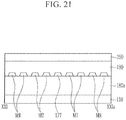
- FIG. 20 is a cross-sectional view of the display device shown in FIG. 18 taken along line XX-XXa, according to an exemplary embodiment of the present disclosure.
- FIG. 21 is a cross-sectional view of the display device shown in FIG. 18 taken along line XXI-XXIa, according to an exemplary embodiment of the present disclosure.
- FIG. 22 is an enlarged view of portion E of the display device shown in FIG. 18 , according to an exemplary embodiment of the present disclosure.
- FIG. 23 is a layout view of a left portion of portion F of the display device shown in FIG. 18 , according to another exemplary embodiment of the present disclosure.
- spatially relative terms such as “beneath”, “below”, “lower”, “under”, “above”, “upper”, etc., may be used herein for ease of description to describe one element or feature's relationship to another element(s) or feature(s) as illustrated in the figures. It will be understood that the spatially relative terms are intended to encompass different orientations of the device in use or operation in addition to the orientation depicted in the figures. For example, if the device in the figures is turned over, elements described as “below” or “beneath” or “under” other elements or features would then be oriented “above” the other elements or features. Thus, the exemplary terms “below” and “under” can encompass both an orientation of above and below.
- a component such as a film, a region, a layer, or an element
- a component such as a film, a region, a layer, or an element
- it can be directly on, connected, coupled, or adjacent to the other component, or intervening components may be present.
- a component when referred to as being “between” two components, it can be the only component between the two components, or one or more intervening components may also be present.
- first”, “second”, “third”, etc. are used herein to distinguish one element from another, and the elements are not limited by these terms.
- a “first” element in an exemplary embodiment may be described as a “second” element in another exemplary embodiment.
- each block, unit, and/or module may be implemented by dedicated hardware, or as a combination of dedicated hardware to perform some functions and a processor (e.g., one or more programmed microprocessors and associated circuitry) to perform other functions.
- each block, unit, and/or module of the exemplary embodiments may be physically separated into two or more interacting discrete blocks, units, and/or modules without departing from the scope of the present disclosure. Further, the blocks, units, and/or modules of the exemplary embodiments may be physically combined into more complex blocks, units, and/or modules without departing from the scope of the present disclosure.
- a display device according to an exemplary embodiment of the present disclosure will be described with reference to FIG. 1 to FIG. 5 .
- a plane structure of the display device is first described with reference to FIG. 1 .
- a cross-sectional structure of the display device is then described with reference to FIG. 2 .
- the display device includes a display panel 1000 including a display area DA and a peripheral area PA, and a circuit unit 750 (also referred to as a defect inspection circuit 750 ).
- the display area DA includes a plurality of pixels PX and a plurality of signal lines disposed on a plane having an x direction and a y direction.
- a structure observed when viewing in a direction substantially perpendicular to the x direction and the y direction is referred to as a plane structure
- a structure observed when cut along the direction substantially perpendicular to the x direction and the y direction is referred to as a cross-sectional structure.
- the signal lines include a plurality of gate lines 121 that transmit a gate signal and a plurality of data lines 171 that transmit a data signal.
- the gate lines 121 extend in the x direction, and the data lines 171 extend in the y direction, thereby crossing the gate lines 121 .
- Each pixel PX may include at least one switching element and a pixel electrode connected thereto.
- the switching element may be implemented as a three-terminal element such as a transistor integrated with the display panel 1000 , and may be connected to at least one gate line 121 and at least one data line 171 .
- the switching element is turned on or turned off according to the gate signal transmitted by the gate line 121 , thereby selectively transmitting the data signal to the pixel electrode.
- each pixel PX may display one of predetermined colors, and an image of a desired color may be recognized by combining images displayed by the predetermined colors.
- An example of the predetermined colors displayed by the plurality of pixels PX may be three primary colors of red, green, and blue, or three primary colors of yellow, cyan, and magenta. At least one different color such as white may be further included as well as the three primary colors.
- the display panel 1000 includes a substrate 110 in which the pixels PX and the signal lines are formed.
- the substrate 110 may include, for example, glass, plastic, etc.
- the display panel 1000 may be a flexible display panel.
- the substrate 110 may be composed of various plastics such as PET, PEN, PC, PAR, PEI, PES, or PI, a metal thin film, or glass.
- the peripheral area PA is positioned outside the display area DA, and surrounds a periphery of the display area DA.
- the peripheral area PA may include a plurality of sensing wires M 1 , M 2 , M 3 , and M 4 .
- the plurality of sensing wires M 1 , M 2 , M 3 , and M 4 are wires used to sense defects such as, for example, cracks, or lifting generated in the peripheral area PA of the display panel 1000 .
- the defects may be sensed through, for example, wire resistance detection.
- FIG. 1 shows an example in which a pair of sensing wires M 1 and M 2 are positioned at a left side and a pair of sensing wires M 3 and M 4 are positioned at a right side with respect to the display area DA.
- exemplary embodiments of the present disclosure are not limited thereto.
- each wire of the sensing wires M 1 , M 2 , M 3 , and M 4 is positioned on only one layer, or is formed by electrically connecting portions positioned at different layers from each other.
- Both ends of each of the sensing wires M 1 , M 2 , M 3 , and M 4 is connected to the circuit unit 750 .
- both ends of each of the sensing wires M 1 , M 2 , M 3 , and M 4 are connected at the same side of the circuit unit 750 .
- Each of the sensing wires M 1 , M 2 , M 3 , and M 4 starts from one end, extends along a left or right edge of the display area DA, and then is curved to again return, thereby having a reciprocating structure (or a meandering shape).
- each of the sensing wires M 1 , M 2 , M 3 , and M 4 moves alternately back and forth (e.g., reciprocates) between extending in the x direction and the y direction.
- a number of reciprocations of one reciprocating structure may be one as shown in the drawing, or may be plural.
- at least one sensing wire from among the plurality of sensing wires M 1 , M 2 , M 3 , and M 4 may have a plurality of reciprocating structures.
- Each of the sensing wires M 1 , M 2 , M 3 , and M 4 may include a portion extending along the left or right edge of the display area DA as shown in FIG. 1 , and a portion extending along an upper edge of the display area DA.
- each of the sensing wires M 1 , M 2 , M 3 , and M 4 extends in the y direction along the left or right edge of the display area DA (the wire may reciprocate several times in the y direction in this portion), and extends in the x direction along the upper edge of the display area DA (the wire may reciprocate several times in the x direction in this portion) after folding in the direction near a corner of the display panel 1000 , and the direction may be folded on a center portion of the upper edge of the display area DA to return.
- each of the sensing wires M 1 , M 2 , M 3 , and M 4 may only include a portion extending along the left or right edge of the display area DA and may not be positioned on the upper edge of the display area DA.
- a pair of sensing wires M 1 and M 2 or M 3 and M 4 positioned in the peripheral area PA of one side with respect to the display area DA may include portions extending to be substantially parallel to each other in the peripheral area PA, and one of the sensing wires M 2 and M 4 may be positioned between one of the other sensing wires M 1 and M 3 and the display area DA. Both ends of a pair of sensing wires M 1 and M 2 or M 3 and M 4 positioned in the peripheral area PA of one side with respect to the display area DA may be connected to the same side of the circuit unit 750 .
- the same side of the circuit unit 750 means one edge extending in a predetermined direction as shown in FIG. 1 , or means one edge toward the predetermined direction when distinguishing the edge as the direction of the edge of the circuit unit 750 .
- Wire resistances of the sensing wires M 1 , M 2 , M 3 , and M 4 may be different from or similar to each other.
- the wire resistances of the sensing wires M 2 and M 4 placed closer to the display area DA are about equal to or smaller than the wire resistances of the sensing wires M 1 and M 3 placed closer to the edge of the display panel 1000 .
- the number of reciprocations of the reciprocating structure included in at least one sensing wire from among the plurality of sensing wires M 1 , M 2 , M 3 , and M 4 may be equal to or different from the number of reciprocations of the reciprocating structure included in other sensing wires M 1 , M 2 , M 3 , and M 4 .
- the number of reciprocations of the reciprocating structure included in the sensing wires M 1 and M 3 positioned further outward relative to the display area DA is smaller than the number of reciprocations of the reciprocating structure included in the sensing wires M 2 and M 4 positioned closer to the display area DA.
- a bezel of the display panel 1000 may be reduced by reducing the size of the peripheral area PA, and a deviation of a wire length depending on the positions of the sensing wires M 1 , M 2 , M 3 , and M 4 may be compensated.
- the sensing wires M 1 , M 2 , M 3 , and M 4 are positioned on the same layer on a cross-section, include the same material, and are formed by being simultaneously patterned in the same manufacturing process.
- the plurality of sensing wires M 1 , M 2 , M 3 , and M 4 may have a similar wire width deviation under an influence of the same or equal process distribution.
- a matching resistor to compensate the resistance deviation of the sensing wires M 1 , M 2 , M 3 , and M 4 having a large difference may be further included in exemplary embodiments.
- At least one wire resistance from among the plurality of sensing wires M 1 , M 2 , M 3 , and M 4 is used as a reference resistance value to compare the wire resistances of the other sensing wires M 1 , M 2 , M 3 , and M 4 with each other.
- a gate driver connected to the plurality of gate lines 121 , which applies the gate signal, is further positioned in the peripheral area PA.
- the peripheral area PA further includes a bending region in which the display panel 1000 is bent or is bendable.
- the bending region is positioned between the display area DA and the circuit unit 750 . The bending region will be described in further detail below.
- the circuit unit 750 is positioned at a printed circuit film 700 connected to the peripheral area PA of the display panel 1000 , as shown in FIG. 1 .
- the circuit unit 750 is directly mounted on the peripheral area PA of the display panel 1000 , or is formed on the substrate 110 along with constituent elements such as, for example, a transistor of the pixel PX.
- a data driver that generates the data signal to drive the pixel PX, and a timing controller may be further positioned in the printed circuit film 700 ,
- the circuit unit 750 may be, for example, an integrated circuit (IC) chip.
- the circuit unit 750 includes a plurality of pad portions connected to each end of the sensing wires M 1 , M 2 , M 3 , and M 4 or bonded to a pad portion connected to each end of the sensing wires M 1 , M 2 , M 3 , and M 4 . As shown in FIG. 2 , in an exemplary embodiment, these pad portions are positioned at a location in which the sensing wires M 1 , M 2 , M 3 , and M 4 and the circuit unit 750 meet.
- the sensing wires M 1 , M 2 , M 3 , and M 4 extend to the printed circuit film 700 .
- the sensing wires M 1 , M 2 , M 3 , and M 4 may include a wire positioned at the display panel 1000 and a wire positioned at the printed circuit film 700 connected to the wire of the display panel 1000 .
- FIG. 2 A cross-sectional structure of the display device according to an exemplary embodiment of the present disclosure will now be described with reference to FIG. 2 along with FIG. 1 .
- a barrier layer 120 may be positioned on a substrate 110 .
- the barrier layer 120 may include a plurality of layers, or may be a single layer as shown in FIG. 2 .
- the active pattern is positioned on the barrier layer 120 .
- the active pattern may include an active pattern 130 positioned in the display area DA and an active pattern 130 d positioned in the peripheral area PA.
- Each of the active patterns 130 and 130 d may include a source region and a drain region, and a channel region positioned therebetween.
- the active pattern may include, for example, amorphous silicon, polysilicon, or an oxide semiconductor.
- a first insulating layer 141 may be positioned on the active patterns 130 and 130 d , and a first conductive layer may be positioned on the first insulating layer 141 .
- the first conductive layer may include a conductor 155 overlapping the active pattern 130 positioned in the display area DA, a conductor 150 d overlapping the active pattern 130 d positioned in the peripheral area PA, and the plurality of above-described gate lines 121 .
- the transistor TRa may function as a switching element included in the pixel PX positioned in the display area DA, and the transistor TRd may function as a switching element included in the gate driver.
- a second insulating layer 142 may be positioned on the first conductive layer and the first insulating layer 141 , and a second conductive layer may be positioned on the second insulating layer 142 .
- the second conductive layer may include at least one of sensing wires M 1 , M 2 , M 3 , and M 4 , but is not limited thereto. At least one sensing wire from among the sensing wires M 1 , M 2 , M 3 , and M 4 may be positioned in a conductive layer other than the second conductive layer.
- a third insulating layer 160 may be positioned on the second conductive layer and the second insulating layer 142 .
- At least one layer from among the first insulating layer 141 , the second insulating layer 142 , and the third insulating layer 160 may include an inorganic insulating material such as, for example, a silicon nitride (SiNx), a silicon oxide (SiOx), and/or an organic insulating material.
- an inorganic insulating material such as, for example, a silicon nitride (SiNx), a silicon oxide (SiOx), and/or an organic insulating material.
- the first insulating layer 141 , the second insulating layer 142 , and the third insulating layer 160 may include a contact hole 165 positioned at the source region and/or the drain region of the transistors TRa and TRd.
- a third conductive layer may be positioned on the third insulating layer 160 .
- the third conductive layer may include a conductor 170 connected to the source region or the drain region of the transistors TRa and TRd through the contact hole 165 , a voltage transmitting line 177 , and the above-described data line 171 .
- the voltage transmitting line 177 may be positioned in the peripheral area PA, and may transmit a predetermined voltage such as, for example, a common voltage ELVSS.
- At least one layer from among the first conductive layer, the second conductive layer, and the third conductive layer may include a conductive material such as, for example, copper (Cu), aluminum (Al), molybdenum (Mo), titanium (Ti), tantalum (Ta), and alloys of at least two of these materials.
- a conductive material such as, for example, copper (Cu), aluminum (Al), molybdenum (Mo), titanium (Ti), tantalum (Ta), and alloys of at least two of these materials.
- a passivation layer 180 is positioned on the third conductive layer and the third insulating layer 160 .
- the passivation layer 180 may include an inorganic insulating material and/or an organic insulating material such as, for example, a polyacrylic resin and a polyimide-based resin.
- An upper surface of the passivation layer 180 may be substantially flat.
- the passivation layer 180 may include a contact hole positioned on the voltage transmitting line 177 positioned in the peripheral area PA.
- a pixel electrode layer is positioned on the passivation layer 180 .
- the pixel electrode layer may include a pixel electrode 191 corresponding to each pixel PX of the display area DA, and a voltage transmitting electrode 197 positioned in the peripheral area PA.
- the voltage transmitting electrode 197 may be physically and electrically connected to the voltage transmitting line 177 through a contact hole of the passivation layer 180 , thereby transmitting the common voltage ELVSS.
- the pixel electrode layer may include, for example, a semi-transmissive conductive material or a reflective conductive material.
- a pixel definition layer 350 is positioned on the passivation layer 180 and the pixel electrode layer.
- the pixel definition layer 350 may have an opening 351 formed on the pixel electrode 191 , and may further include at least one dam portion 350 d positioned at the peripheral area PA.
- the dam portion 350 d may extend to be substantially parallel to the edge of the substrate 110 on a plane.
- a spacer 360 d may be positioned on the dam portion 350 d.
- At least one of the sensing wires M 1 , M 2 , M 3 , and M 4 may be positioned outside relative to the dam portion 350 d .
- the location of the at least one of the sensing wires M 1 , M 2 , M 3 , and M 4 is not limited thereto.
- at least one sensing wire from among the sensing wires M 1 , M 2 , M 3 , and M 4 may be positioned inside relative to the dam portion 350 d.
- the voltage transmitting electrode 197 includes a portion that is not covered by the pixel definition layer 350 .
- the pixel definition layer 350 may include a photosensitive material such as, for example, a polyacrylic resin and a polyimide-based resin.
- An emission layer 370 is positioned on the pixel electrode 191 .
- the emission layer 370 may include a portion positioned in the opening 351 of the pixel definition layer 350 .
- the emission layer 370 may further include at least one dummy emission layer 370 d positioned in the peripheral area PA and positioned on the pixel definition layer 350 .
- the emission layer 370 may include, for example, an organic emission material or an inorganic emission material.
- a common electrode 270 is positioned on the emission layer 370 .
- the common electrode 270 is also formed on the pixel definition layer 350 .
- the common electrode 270 may be continuously formed throughout the plurality of pixels PX.
- the common electrode 270 may be physically and electrically connected to the voltage transmitting electrode 197 in the peripheral area PA, thereby receiving the common voltage ELVSS.
- the common electrode 270 may include, for example, a conductive transparent material.
- the pixel electrode 191 , the emission layer 370 , and the common electrode 270 of each pixel PX together form a light emitting diode (LED) ED, one of the pixel electrode 191 and the common electrode 270 functions as a cathode, and the other one of the pixel electrode 191 and the common electrode 270 functions as an anode.
- LED light emitting diode
- An encapsulating portion 380 that protects and encapsulates the light emitting diode (LED) ED may be positioned on the common electrode 270 .
- the encapsulating portion 380 includes at least one of inorganic layers 381 and 383 and at least one organic layer 382 .
- the at least one of the inorganic layers 381 and 383 and the at least one organic layer 382 may be alternately stacked.
- the organic layer 382 includes the organic material, thereby having a flattening characteristic.
- the inorganic layers 381 and 383 may include an inorganic material such as, for example, an aluminum oxide (AlOx), a silicon oxide (SiOx), a silicon nitride (SiNx), and a silicon oxynitride (SiON).
- AlOx aluminum oxide
- SiOx silicon oxide
- SiNx silicon nitride
- SiON silicon oxynitride
- the two inorganic layers 381 and 383 may be in contact with each other in the peripheral area PA.
- the inorganic layer 381 positioned at the bottom of the inorganic layers 381 and 383 may be in contact with the upper surface of the third insulating layer 160 in the peripheral area PA.
- exemplary embodiments of the present disclosure are not limited thereto.
- the edge of the organic layer 382 included in the encapsulating portion 380 may be positioned between the dam portion 350 d and the display area DA.
- the dam portion 350 d may function to prevent the organic material from overflowing to the outside when forming the organic layer 382 of the encapsulating portion 380 .
- a buffer layer 389 including the inorganic insulating material and/or the organic insulating material is positioned on the encapsulating portion 380 .
- the buffer layer 389 is not present.
- a fourth conductive layer may be positioned on the buffer layer 389 .
- the fourth conductive layer may include a first touch conductor TEa.
- a first touch insulating layer 391 may be positioned on the fourth conductive layer, and a fifth conductive layer may be positioned thereon.
- the fifth conductive layer may include a second touch conductor TEb.
- a second touch insulating layer 392 may be positioned on the fifth conductive layer.
- the first touch conductor Tea and the second touch conductor TEb form a capacitive touch sensor.
- FIG. 3 is an enlarged view of portion A of the display device shown in FIG. 1 .
- FIG. 4 is a plane layout view of a sensing wire and an end of a signal wire positioned at portion A of the display device shown in FIG. 1 .
- FIG. 5 is a plane layout view showing an arrangement of pad portions of a circuit unit of the display device shown in FIG. 1 .
- the circuit unit 750 inputs input signals In_M 1 , In_M 2 , In_M 3 , and In_M 4 as defect test signals, which are used to detect defects such as a crack, to one end of each of the sensing wires M 1 , M 2 , M 3 , and M 4 . Further, the circuit unit 750 receives output signals Out_M 1 , Out_M 2 , Out_M 3 , and Out_M 4 from the other end of sensing wires M 1 , M 2 , M 3 , and M 4 .
- Output signal Out_M 1 corresponds to sensing wire M 1
- output signal Out_M 2 corresponds to sensing wire M 2
- output signal Out_M 3 corresponds to sensing wire M 3
- output signal Out_M 4 corresponds to sensing wire M 4 .
- the circuit unit 750 includes a comparator unit 751 (also referred to as a comparator circuit 751 ), a plurality of resistance detection units 752 and 753 (also referred to as a plurality of resistance detection circuits 752 and 753 ), a plurality of determining units 754 and 755 (also referred to as a plurality of determining circuits 754 and 755 ), a memory 756 , and a controller 757 (also referred to as a controller circuit 757 ).
- a comparator unit 751 also referred to as a comparator circuit 751
- a plurality of resistance detection units 752 and 753 also referred to as a plurality of resistance detection circuits 752 and 753
- a plurality of determining units 754 and 755 also referred to as a plurality of determining circuits 754 and 755
- a memory 756 also referred to as a controller circuit 757
- FIG. 3 shows an exemplary embodiment in which the circuit unit 750 includes a pair of resistance detection units 752 and 753 respectively corresponding to the left sensing wires M 1 and M 2 and the right sensing wires M 3 and M 4 .
- the number of resistance detection units is not limited thereto.
- the number of resistance detection units may be the same as the number of sensing wires M 1 , M 2 , M 3 , and M 4 connected to the circuit unit 750 .
- one resistance detection unit may be provided for all sensing wires M 1 , M 2 , M 3 , and M 4 .
- the resistance detection unit 752 detects the resistance of the sensing wires M 1 and M 2 based on the output signals Out_M 1 and Out_M 2 of the sensing wires M 1 and M 2
- the resistance detection unit 753 detects the resistance of the sensing wires M 3 and M 4 based on the output signals Out_M 3 and Out_M 4 of the sensing wires M 3 and M 4 .
- the resistance detection units 752 and 753 respectively include at least one analog-to-digital converter (ADC), which converts the output signals Out_M 1 , Out_M 2 , Out_M 3 , and Out_M 4 from the sensing wires M 1 , M 2 , M 3 , and M 4 to a digital value.
- ADC analog-to-digital converter
- the resistance detection units 752 and 753 output each detected resistance of the sensing wires M 1 , M 2 , M 3 , and M 4 to the comparator unit 751 and the determining units 754 and 755 .
- the resistance detection units 752 and 753 transmit the detected resistances of the sensing wires M 1 , M 2 , M 3 , and M 4 to the memory 756 , and the memory 756 stores the detected resistances.
- FIG. 3 shows an exemplary embodiment in which the circuit unit 750 includes a pair of determining units 754 and 755 respectively corresponding to the resistance detection units 752 and 753 .
- the number of determining units 754 and 755 is not limited thereto.
- the number of determining units may be the same as the number of sensing wires M 1 , M 2 , M 3 , and M 4 connected to the circuit unit 750 .
- one determining unit may be provided for both resistance detection units 752 and 753 .
- the determining unit 754 determines whether each resistance of the sensing wires M 1 and M 2 input from the resistance detection unit 752 is within a first predetermined range, and outputs the determined result.
- the determining unit 755 determines whether each resistance of the sensing wires M 3 and M 4 input from the resistance detection unit 753 is within the first predetermined range, and outputs the determined result.
- the determined result of the determining units 754 and 755 may be included in the output signals OUT 1 and OUT 2 , and thus, may be output outside the circuit unit 750 (e.g., the determined results may be transmitted to a device external to the circuit unit 750 ).
- the resistance of the sensing wires M 1 , M 2 , M 3 , and M 4 may be stored in the memory 756 depending on the determined result of the determining units 754 and 755 .
- the determining unit 754 is connected to the signal wire W 1 positioned at the substrate 110 or the printed circuit film 700 , and outputs the output signal OUT 1 to the signal wire W 1 .
- the determining unit 755 is connected to the signal wire W 2 positioned at the substrate 110 or the printed circuit film 700 , and outputs the output signal OUT 2 to the signal wire W 2 .
- the comparator unit 751 includes a plurality of comparators 751 a , 751 b , 751 c , and 751 d .
- FIG. 3 shows an exemplary embodiment in which the comparator unit 751 includes four comparators 751 a , 751 b , 751 c , and 751 d .
- the number of comparators is not limited thereto.
- the comparator 751 a compares the resistance of the sensing wire M 1 and the resistance of the sensing wire M 2 detected by the resistance detection unit 752 with each other, and outputs the determined result.
- the comparator 751 b compares the resistance of the sensing wire M 3 and the resistance of the sensing wire M 4 detected by the resistance detection unit 753 with each other, and outputs the determined result.
- the comparator 751 c compares the resistance of the sensing wire M 1 or the sensing wire M 2 detected by the resistance detection unit 752 with the resistance of the sensing wire M 3 or the sensing wire M 4 detected by the resistance detection unit 753 , and outputs the determined result.
- the comparator 751 c compares the resistance of the sensing wire M 1 or M 2 positioned in the peripheral area PA of one side (e.g., the left side) with respect to the display area DA with the resistance of the sensing wire M 3 or M 4 positioned at the other side (e.g., the right side), and outputs the determined result.
- the comparator 751 d compares the results of a plurality of inspection operations, which will be described further below, with each other, and outputs the determined result.
- the comparator 751 d receives the result of each inspection operation from the memory 756 .
- the comparison result of the comparator unit 751 including the comparison result of the comparator 751 d may be included in the output signal OUT 3 to be output outside the circuit unit 750 , and may be transmitted to and stored in the memory 756 .
- the comparator unit 751 is connected to the signal wire W 3 positioned at the substrate 110 or the printed circuit film 700 , and outputs the output signal OUT 3 to the signal wire W 3 .
- the controller 757 receives an input control signal Cont from the outside (e.g., from a source disposed external to the circuit unit 750 ), and uses the input control signal Cont to control each part of the circuit unit 750 .
- the control signal Cont may be used to configure the settings of the memory 756 .
- the controller 757 is connected to the signal wire W 4 positioned at the substrate 110 or the printed circuit film 700 , and receives the input control signal Cont from the outside. Alternatively, the controller 757 may be positioned outside the circuit unit 750 .
- the sensing wires M 1 , M 2 , M 3 , and M 4 , and the signal wires W 1 , W 2 , W 3 , and W 4 positioned at the substrate 110 or the printed circuit film 700 may include pad portions P 1 that function as terminals positioned at the end of the wires.
- the pad portion P 1 may be positioned at the same layer and made of the same material as the sensing wires M 1 , M 2 , M 3 , and M 4 and the signal wires W 1 , W 2 , W 3 , and W 4 .
- the pad portion P 1 may be positioned at different layers.
- the circuit unit 750 includes a plurality of pad portions P 2 that function as terminals connected to the pad portions P 1 .
- the pad portions P 2 of the circuit unit 750 may be disposed to respectively correspond to the pad portions P 1 , and the pad portions P 2 and the pad portions P 1 may be electrically bonded to each other through various bonding methods.
- the pad portions P 2 of the circuit unit 750 may be respectively connected to the resistance detection units 752 and 753 , the determining units 754 and 755 , the comparator unit 751 , and the controller 757 .
- only one sensing wire is positioned in the peripheral area PA at one side of the display area DA.
- one of the sensing wires M 1 and M 2 shown in FIG. 1 and FIG. 2 may be omitted, one of the sensing wires M 3 and M 4 may be omitted, or one of the sensing wires M 1 and M 2 and one of the sensing wires M 3 and M 4 may be omitted.
- At least one of two comparators 751 a and 751 b may be omitted, and the pad portions P 1 and P 2 connected to the omitted sensing wire may be omitted.
- the comparator 751 c of the comparator unit 751 may be omitted, thereby only including the comparator 751 d .
- the comparator 751 d may compare the results of the plurality of inspection steps executed at different times with each other to determine a progress degree of a defect such as a crack, and the determined result of the progress and the progress degree may be included in the output signal OUT 3 to be output.
- a progress degree indicates whether a defect such as a crack is getting worse.
- the sensing wire may be positioned at only one side of the display area DA in the exemplary embodiment shown in FIG. 1 .
- the sensing wires M 1 and M 2 may be omitted or the sensing wires M 3 and M 4 may be omitted.
- one of the two comparators 751 a and 751 b and the comparator 751 c may be omitted, and the pad portions P 1 and P 2 connected to the omitted sensing wire may be omitted.
- only one sensing wire may be positioned in the peripheral area PA positioned on one side of the display area DA.
- the comparator unit 751 may only include the comparator 751 d , and the comparator 751 d may compare the results of the plurality of inspection steps executed at different times with each other to determine the progress and the progress degree of a defect such as a crack.
- the signal wires W 1 and W 2 and the pad portion P 2 of the circuit unit 750 may be omitted.
- an inspecting method includes performing a first inspection operation S 61 and subsequently performing a second inspection operation S 62 after performing the first inspection operation S 61 .
- the first inspection operation S 61 may be referred to as a primary inspection operation, and the second inspection operation may be referred to as a secondary inspection operation.
- a first inspection result may be referred to as a primary inspection result, and a second inspection result may be referred to as a secondary inspection result.
- the method compares the result (the information related to the resistance of the sensing wire) of the first inspection operation and the result (the information related to the sensing wire) of the second inspection operation with each other, and uses this comparison result to determine whether a defect is present in the display device at operation S 63 .
- the determination made in operation S 63 may include determining the existence of the defect (e.g., a crack), as well as the progress and the progress degree of the defect (e.g., the crack) in the display panel 1000 . This determined result may be included in the above-described output signal OUT 3 to be output.
- a defect detected in the display panel 1000 may be referred to as a crack.
- exemplary embodiments of the present disclosure are not limited thereto, and exemplary embodiments may be utilized to determine defects other than a crack.
- An additional inspection operation (e.g., a third inspection operation, a fourth inspection operation, etc.) executed after the second inspection operation may be further included in exemplary embodiments.
- the inspection operations S 61 and S 62 (as well as any additional inspection operations) may be substantially the same.
- the inspection result of each of the first inspection operation S 61 and the second inspection operation S 62 may include, for example, information including a resistance value indicating the wire resistance of each of the sensing wires M 1 , M 2 , M 3 , and M 4 , and/or information including a resistance comparison value indicating a comparison result between resistances of different wires from among the sensing wires M 1 , M 2 , M 3 , and M 4 .
- Such information may be referred to herein as resistance information
- Resistance information obtained during a first inspection operation may be referred to as first resistance information
- resistance information obtained during a second inspection operation may be referred to as second resistance information, etc.
- the first inspection operation S 61 and the second inspection operation S 62 include information including a resistance value indicating the resistance of one of the sensing wires (e.g., sensing wire M 1 ) at the time of the first inspection operation S 61 and at the time of the second inspection operation S 62 .
- the first inspection operation S 61 and the second inspection operation S 62 include information including a resistance comparison value indicating a comparison result between the resistance of two different wires (e.g., sensing wires M 1 and M 2 ) at the time of the first inspection operation S 61 and at the time of the second inspection operation S 62 .
- each inspection operation such as the first inspection operation S 61 and the second inspection operation S 62 , according to an exemplary embodiment of the present disclosure, will be described with reference to FIG. 7 as well as the above-described figures.
- the circuit unit 750 respectively inputs the input signals In _M 1 , In_M 2 , In_M 3 , and In_M 4 to the plurality of sensing wires M 1 , M 2 , M 3 , and M 4 , and receives the output signals Out_M 1 and Out_M 2 , Out_M 3 , and Out_M 4 .
- the resistance detection units 752 and 753 of the circuit unit 750 detect each wire resistance of the sensing wires M 1 , M 2 , M 3 , and M 4 based on the output signals Out_M 1 , Out_M 3 , and Out_M 4 (S 71 ), and the determining unit 754 determines whether the detected resistance is within a first predetermined range.
- the first predetermined range may be, for example, a range of about ⁇ 15% to about +15% with respect to a center value (e.g., about 500 k ⁇ , about 600 k ⁇ , about 700 k ⁇ , etc.) of the resistance, however, the first predetermined range is not limited thereto.
- the first predetermined range may be stored in the memory 756 . If each wire resistance of the sensing wires M 1 , M 2 , M 3 , and M 4 is within the first predetermined range, it may be determined that the wires are in the normal wire state within a process dispersion range, and thus, that the display panel 1000 may be in good condition. Otherwise, if each wire resistance of the sensing wires M 1 , M 2 , M 3 , and M 4 is outside of the first predetermined range, it is determined that a defect (e.g., a crack) is present in the display panel 1000 .
- a defect e.g., a crack
- each determining unit described herein may compare a resistance value to an upper threshold value and a lower threshold value to determine whether the resistance value is within a predetermined range. When the resistance value is between the upper threshold value and the lower threshold value, the resistance value is determined to be within the predetermined range.
- each detected resistance of the sensing wires M 1 , M 2 , M 3 , and M 4 is stored in the memory 756 (S 72 ), and the comparators 751 a , 751 b , and 751 c of the comparator unit 751 compare the resistances of the sensing wires M 1 , M 2 , M 3 , and M 4 detected from the resistance detection units 752 and 753 with each other, thereby determining whether a resistance comparison value (e.g., a difference between resistances, or a ratio between the resistances) is within a second predetermined range (S 73 ).
- a resistance comparison value e.g., a difference between resistances, or a ratio between the resistances
- the second predetermined range may be determined as a range (e.g., within about 15%) of the ratio for the reference resistance of the resistance comparison value.
- the second predetermined range may be stored in the memory 756 . If the resistance comparison value is within the second predetermined range, it may be determined that the display panel 1000 is in good condition, otherwise, it is determined that a defect (e.g., a crack) is present in the display panel 1000 . Detection sensitivity may be controlled through the control of the second predetermined range. The control of the second predetermined range may be executed through the controller 757 .
- the second predetermined range may have a plurality of ranges that are different from each other, thereby allowing for the determination of a crack progress degree (e.g., the severity/degree that the crack is progressing).
- the second predetermined range may have a plurality of ranges divided into a plurality of levels such as 3%, 5%, 7%, 9%, 12%, 15%, 20%, 25%, 30%, and 40%.
- the detailed information for the progress degree of the crack may be obtained by determining whether the resistance comparison value (the difference or the ratio) is within any range from among the plurality of ranges.
- a fine crack degree may be sensed by determining whether the resistance comparison value is within any range from among a relatively small range (e.g., less than 15%) the second predetermined range.
- the sensing wires M 1 , M 2 , M 3 , and M 4 are simultaneously formed in the same manufacturing process, they are affected by the same process dispersion, thereby having equal wire width deviation, and the sensing wires M 1 , M 2 , M 3 , and M 4 may each be a reference wire for each other capable of comparing the change of the wire resistance.
- the crack generation may be sensed in the left peripheral area PA of the display area DA by using the resistance comparison value between the wire resistances of the sensing wire M 1 and the sensing wire M 2 positioned at the left side with respect to the display area DA, and the crack generation may be sensed in the right peripheral area PA of the display area DA by using the resistance comparison value between the wire resistances of the sensing wire M 3 and the sensing wire M 4 positioned at the right side with respect to the display area DA.
- the aspect or the degree of the crack generated in two wires may be different if the crack is generated in the peripheral area PA. Accordingly, when the defect such as the crack is generated in the display panel 1000 , the crack generation may be sensed by using the difference between the wire resistances of the sensing wires M 1 and M 2 or M 3 and M 4 positioned at the same side with respect to the display area DA.
- the defect generation such as the crack in the peripheral area PA may be correctly determined through the comparison between the resistances of the sensing wires (one of M 1 and M 2 and one of M 3 and M 4 ) positioned at the peripheral area PA of the different sides from each other with respect to the display area DA.
- the resistance comparison value is stored in the memory 756 (S 74 ).
- the crack generation of the display panel is sensed by an analog method by applying a voltage to a sensing wire to sense the crack and inspecting a lighting state of the display panel, an error detection probability is high depending on the resistance change due to the wire width deviation (10 to 15%) in the sensing wire by the process dispersion, visual inspection is difficult, and the crack degree may not be recognized.
- the crack generation of the display panel 1000 is inspected by a digital method through the circuit unit 750 , the inspection of the defect generation such as the crack is improved.
- the error detection according to the process dispersion may be prevented, thereby increasing defect inspection accuracy.
- the detailed information for the progress degree of the crack may be obtained, and a fine crack may also be sensed/detected.
- the comparator unit 751 since the comparator unit 751 is controlled, the sensitivity of the detection of the defect generation such as the crack may be controlled. Further, the first predetermined range and the second predetermined range may be controlled. The control of the comparator unit 751 , the first predetermined range, and the second predetermined range, may be obtained through the controller 757 .
- the information including the resistance values of the sensing wires M 1 , M 2 , M 3 , and M 4 stored in the memory 756 in each of the first inspection operation 861 and the second inspection 861 , and/or the information including the resistance comparison values between the sensing wires M 1 , M 2 , M 3 , and M 4 may be compared with each other to determine the progress of the crack and the progress degree. This is further described with reference to FIG. 8 and FIG. 9 .
- FIG. 8 and FIG. 9 are tables showing an example of storing a result of a first inspection operation and a second inspection operation in the memory 756 in a method of inspecting a display device to identify a defect such as a crack in the display device, according to an exemplary embodiment of the present disclosure.
- the resistance of one of the sensing wires M 1 , M 2 , M 3 , or M 4 is detected as 170 k ⁇ as the first inspection result such that a number 4 (or 170 k ⁇ ) is stored in the memory 756
- the resistance of the corresponding sensing wire M 1 , M 2 , M 3 , or M 4 is detected as 185 k ⁇ as a second inspection result such that a number 7 (or 185 k ⁇ ) is stored in the memory 756 .
- the resistance of a range that is not shown in the table of FIG. 8 may be stored as a number immediately before or after the corresponding resistance depending on a setting.
- the detected resistance in the case of 173 k ⁇ may be stored as the number 4 or 5.
- the comparator 751 d of the comparator unit 751 compares the resistances detected in the first inspection operation S 61 and the second inspection S 62 , when a resistance difference is not generated, it may be determined that the progress of the crack is not generated (e.g., a crack is not getting worse), when the difference of the resistance is larger than 0 and is larger than a third predetermined range, it may be determined that the progress degree of the crack is large, and when the difference of the resistance is larger than 0 and is smaller than the third predetermined range, it may be determined that the progress degree of the crack is small.
- the third predetermined range may be stored in the memory 756 . For example, in FIG.
- the resistance of the second inspection result is larger than the resistance of the first inspection result, it may be determined that progress is occurring in the crack of the display panel 1000 (e.g., the crack is getting worse), and if the third predetermined range is set as No. 3, it may be determined that the progress degree of the crack is relatively large.
- the resistance comparison value of two sensing wires from among M 1 , M 2 , M 3 , and M 4 is detected as 6% as the first inspection result such that the number 4 (or 6%) is stored in the memory 756 , and the resistance comparison value is detected as 9% as the second inspection result such that the number 7 (or 9%) is stored in the memory 756 .
- the comparator 751 d of the comparator unit 751 compares the resistance comparison valued detected in the first inspection operation S 61 and the second inspection operation S 62 , when a difference is not generated, it may be determined that the progress of the crack is not generated (e.g., the crack is not getting worse), when the difference is larger than 0 and is larger than a fourth predetermined range, the progress degree of the crack may be determined to be large, and when the difference of the crack is larger than 0 and is smaller than the fourth predetermined range, the progress degree of the crack may be determined to be small.
- the fourth predetermined range may be stored in the memory 756 . For example, in FIG.
- the progress degree of the crack may be determined to be relatively large.
- the step of determining whether the resistance of the sensing wires M 1 , M 2 , M 3 , and M 4 is within the first predetermined range (S 71 ) and the step of storing the resistance of each of the sensing wires M 1 , M 2 , M 3 , and M 4 (S 72 ) may be omitted, and only the step of comparing the detected resistances (S 73 ) and the step of storing the resistance comparison value between the sensing wires M 1 , M 2 , M 3 , and M 4 (S 74 ) may be performed.
- only the operation S 71 and the operation S 72 may be performed, and the operation S 73 and the operation S 74 may be omitted.
- the circuit unit 750 may further include a comparator that compares the resistance results of two sensing wires positioned at a same side with respect to the display area DA or positioned at opposing different sides with respect to the display area DA. In this case, the circuit unit 750 may determine whether the crack is generated at any side with respect to the display area DA, and if additional cracks are generated at any side.
- the resistance difference between the two wires M 1 and M 2 or M 3 and M 4 positioned at one side (referred to as a first side) with respect to the display area DA is larger than the resistance difference between two wires (one of M 1 and M 2 and one of M 3 and M 4 ) positioned at the other side with respect to the display area DA, it may be determined that the crack is generated, or additional cracks are generated, in the peripheral area PA of the first side, while in the opposite case, it may be determined that the crack is generated, or additional cracks are generated, in the peripheral area PA of the side opposite to the first side.
- the resistances of two sensing wires positioned at opposite sides to each other with respect to the display area DA may be compared through the comparator 751 c to determine the defect generation such as the crack in the peripheral area PA.
- two sensing wires (M 1 and M 2 or M 3 and M 4 ) positioned at the peripheral area PA of the same side with respect to the display area DA may extend in different directions from each other.
- the probability that the crack does not simultaneously occur in two sensing wires (M 1 and M 2 or M 3 and M 4 ) may be high. Accordingly, it may be determined whether the defect such as the crack occurs in the display panel 1000 through the resistance comparison of two sensing wires (M 1 and M 2 or M 3 and M 4 ).
- the wire resistance comparison between the sensing wires M 1 , M 2 , M 3 , and M 4 to sense/detect the defect such as the crack of the display panel 1000 and/or the comparison of the results of the plurality of inspection operations may be performed using various other methods.
- the display device according to the present exemplary embodiment is substantially the same as the previously described exemplary embodiment (including the display panel 1000 a that is substantially the same as the display panel 1000 of the previous exemplary embodiment), however, at least one sensing wire from among the sensing wires M 1 , M 2 , M 3 , and M 4 has a plurality of reciprocating structures U 1 and U 2 .
- FIG. 10 shows an exemplary embodiment in which the sensing wires M 1 and M 3 as a part of the plurality of sensing wires M 1 , M 2 , M 3 , and M 4 have the plurality of reciprocating structures U 1 and U 2 .
- At least one of the sensing wires M 1 , M 2 , M 3 , and M 4 having the plurality of reciprocating structures U 1 and U 2 reciprocates in plural in the y direction in the peripheral area PA of the right or the left with respect to the display area DA to form the reciprocating structure U 1 , then reciprocates in plural in the x direction in the peripheral area PA of the upper side of the display area DA to form the reciprocating structure U 2 , and then is returned to be connected to the circuit unit 750 .
- the sensing wires M 2 and M 4 may also have a plurality of reciprocating structures like the sensing wires M 1 and M 3 .
- the entire wire length of the sensing wires M 2 and M 4 may be shorter than the entire wire length of the sensing wires M 1 and M 3 having the plurality of reciprocating structures U 1 and U 2 .
- the area of the region occupied by the sensing wires M 2 and M 4 may be smaller than the area of the region occupied by the sensing wires M 1 and M 3 .
- the number of reciprocations of the reciprocating structure of the part of the sensing wires M 2 and M 4 may be reduced and/or the wire length may be reduced to reduce the region occupied with the sensing wires M 1 , M 2 , M 3 , and M 4 to reduce a bezel region of the display device.
- the circuit unit 750 may additionally perform a step of compensating the difference of the wire resistance of the sensing wires M 2 and M 4 for the sensing wires M 1 and M 3 .
- the resistance difference according to the wire length difference between the sensing wires M 1 and M 3 and the sensing wires M 2 and M 4 may be compensated by applying (e.g., multiplying) a weight value by the detected resistance of the sensing wires M 2 and M 4 .
- the circuit unit 750 may compensate the wire resistance deviation by a method of determining whether the wire resistance value of the sensing wires M 2 and M 4 is within any region from among regions divided into 20%, 40%, 60%, 80%, and 100% of the wire resistance of the sensing wires M 1 and M 3 to apply the weight value corresponding thereto.
- the circuit unit 750 may apply the weight value to the detected resistance of the sensing wire by the method described above to compensate the difference of the wire resistance.
- the display device according to the present exemplary embodiment is substantially the same as the previously described exemplary embodiments (including the display panel 1000 b that is substantially the same as the display panels 1000 and 1000 a of the previous exemplary embodiments), however, only a pair of sensing wires M 5 and M 6 are positioned in the entire peripheral area PA, thereby reducing the region occupied with the sensing wire in the peripheral area PA and reducing the number of pad portions of a circuit unit 750 a.
- One end of the sensing wire M 5 may be connected to one side of the circuit unit 750 a and the other end thereof may be connected to the other side of the circuit unit 750 a (e.g., the opposite side).
- the sensing wire M 5 starts from one end and extends along the edge of at least three surfaces including the left side, the upper side, and the right side of the display area DA to be extended to the other end.
- the sensing wire M 5 extending along the periphery of the display area DA may have at least one reciprocating structure (or a meandering shape) that is partially reciprocated in plural.
- the plurality of reciprocating structures may be connected to each other, thereby forming one wire.
- One end of the sensing wire M 6 may be connected to one side of the circuit unit 750 a and the other end thereof may be connected to the other side of the circuit unit 750 a .
- the structure of the sensing wire M 6 may be similar to that of the sensing wire M 5 .
- the wire resistances of two sensing wires M 5 and M 6 may be different from each other or may be similar to each other.
- the wire resistance of the sensing wire M 6 may be smaller than the wire resistance of the sensing wire M 5 , and in this case, the number of reciprocations of the reciprocating structure included in the sensing wire M 6 may be smaller than the number of reciprocations of the reciprocating structure included in the sensing wire M 5 .
- the sensing wire M 6 may be positioned between the sensing wire M 5 and the display area DA, however, the position of the sensing wire M 6 is not limited thereto.
- the positions of the sensing wire M 5 and the sensing wire M 6 shown in FIG. 11 may be exchanged with each other.
- the circuit unit 750 a is substantially the same as the above-described circuit unit 750 , however, the circuit unit 750 a may input the input signals In_M 5 and In_M 6 as the crack defect test signal to one end of each of the sensing wires M 5 and M 6 , and may receive the output signals Out_M 5 and Out_M 6 from the other end of the sensing wires M 5 and M 6 .
- the circuit unit 750 a may include a comparator unit 751 A, a resistance detection unit 753 a , a determining unit 754 a , a memory 756 a , and a controller 757 a . These components are substantially the same as the comparator unit 751 , the resistance detection unit 753 , the determining unit 754 , the memory 756 , and the controller 757 described above, respectively. For convenience of explanation, only differences regarding these components are described herein.
- the resistance detection unit 753 a detects the wire resistance of the sensing wires M 5 and M 6 based on the output signals Out_M 5 and Out_M 6 of the sensing wires M 5 and M 6 .
- the resistance detection unit 753 a outputs the detected resistance of each of the sensing wires M 5 and M 6 to the comparator unit 751 A and the determining unit 754 a .
- the resistance detection unit 753 a stores the detected resistance of the sensing wires M 5 and M 6 in the memory 756 a.
- the determining unit 754 a determines whether each resistance of the sensing wires M 5 and M 6 input from the resistance detection unit 753 a is in the first predetermined range to output the determined result.
- the determined result may be included in the output signal OUT, and may be output outside the circuit unit 750 a .
- the resistance of the sensing wires M 5 and M 6 may be stored in the memory 756 a according to the determined result of the determining unit 754 a.
- the comparator unit 751 A is substantially the same as the above-described comparator unit 751 , however, the comparator that compares the resistance of the sensing wire M 5 and the resistance of the sensing wire M 6 to output the determined result, and the comparator that compares the results of the plurality of inspection operations to output the determined result, may be included.
- the comparator unit 751 A may receive the result of each inspection operation from the memory 756 a .
- the comparison result of the comparator unit 751 A may be included in the output signal OUT 4 to be output outside the circuit unit 750 a and to be stored in the memory 756 a.
- the controller 757 a may receive the input control signal Cont from the outside to control each part of the circuit unit 750 a , including, for example, the setting of the memory 756 a.
- circuit unit 750 a The other characteristics of the circuit unit 750 a are substantially the same as those of the circuit unit 750 of the previous exemplary embodiment. For convenience of explanation, a repetitive description thereof is omitted. Further, the inspecting method of the plurality of inspection operations is substantially the same as the above-described inspecting method, and a repetitive description thereof is omitted.
- the display device according to the present exemplary embodiment is substantially the same as the previously described exemplary embodiments (including the display panel 1000 c that is substantially the same as the display panels 1000 and 1000 a of the previous exemplary embodiments), however, the above-described sensing wires M 2 and M 4 are omitted, and only one of the sensing wires M 1 and M 3 is positioned in the peripheral area PA of one side with respect to the display area DA.
- a circuit unit 750 b may include resistance detection units 752 b and 753 b , a comparator unit 751 B, determining units 754 b and 755 b , a memory 756 b , and a controller 757 b . These components are substantially the same as the resistance detection units 752 and 753 , the comparator unit 751 , the determining units 754 and 755 , the memory 756 , and the controller 757 as described above, respectively. For convenience of explanation, only differences relating to these components are described herein.
- the resistance detection unit 752 b detects the wire resistance of the sensing wire M 1 based on the output signal Out_M 1 from the sensing wire M 1
- the resistance detection unit 753 b detects the wire resistance of the sensing wire M 3 based on the output signal Out_M 3 from the sensing wire M 3
- the resistance detection units 752 b and 753 b output the detected resistance of each of the sensing wires M 1 and M 3 to the comparator unit 751 B and the determining units 754 b and 755 b .
- the resistance detection units 752 b and 753 b store the detected resistance of the sensing wires M 1 and M 3 in the memory 756 b.
- the comparator unit 751 B is substantially the same as the above-described comparator unit 751 , however, the comparator that compares the resistances of the sensing wires M 1 and M 3 to output the determined result and the comparator that compares the results of the plurality of inspection operations to output the determined result is included.
- the comparator unit 751 B receives the result of each inspection operation from the memory 756 b .
- the comparison result of the comparator unit 751 B may be included in the output signal OUT 7 to be output outside the circuit unit 750 b and to be stored in the memory 756 b.
- the determining unit 754 b determines whether the resistance of the sensing wire M 1 input from the resistance detection unit 752 b is included in the first predetermined range to output the determined result, and the determining unit 755 b determines whether the resistance of the sensing wire M 3 input from the resistance detection unit 753 b is included in the first predetermined range to output the determined result.
- the determined result of the determining units 754 b and 755 b may be included in the output signals OUT 5 and OUT 6 to be output outside the circuit unit 750 b , and the resistance of the sensing wires M 1 and M 3 may be stored in the memory 756 b according to the determined result of the determining units 754 b and 755 b.
- the controller 757 b may receive the input control signal Cont from the outside to control each part of the circuit unit 750 b , including, for example, the setting of the memory 756 b.
- the resistance of the sensing wires M 1 and M 3 detected through the resistance detection units 752 b and 753 b may be stored in the memory 756 b of the circuit unit 750 b and may be output outside.
- the circuit unit 750 b respectively inputs the input signals In_M 1 and In_M 3 to the sensing wires M 1 and M 3 , and receives the output signals Out_M 1 and Out_M 3 .
- the resistance detection units 752 b and 753 b respectively detect the resistance of the sensing wires M 1 and M 3 based on the output signals Out_M 1 and Out_M 3 , and the determining units 754 b and 755 b determine whether the detected resistance is within the first predetermined range (S 151 ).
- the first predetermined range may be determined with the range within about ⁇ 3%, 6%, 9%, 12%, 15%, 20%, or 30% for the center value (e.g., about 500 k ⁇ , 600 k ⁇ , 700 k ⁇ , etc.) of the resistance, however, exemplary embodiments are not limited thereto. If the resistance of the sensing wires M 1 and M 3 is within the first predetermined range, it is determined that the sensing wires M 1 and M 3 are in the normal wire state within the process dispersion range, and the display panel may be determined to be good, otherwise, the display panel is determined to be bad.
- each detected resistance of the sensing wires M 1 and M 3 is stored in the memory 756 b (S 152 ).
- the comparator unit 751 B may further perform a step of comparing the resistances of the sensing wires M 1 and M 3 detected in the resistance detection units 752 b and 753 b with each other, and determining whether the resistance comparison values (the difference or the ratio between the resistances) are within the second predetermined range (as described above with reference to FIG. 7 ). If the resistance comparison value is within the second predetermined range, the display panel may be determined to be good, otherwise the display panel may be determined to be bad.
- circuit unit 750 b may be substantially the same as those of the circuit unit 750 of the previous exemplary embodiment, and the inspecting method may also be substantially the same as the above-described inspecting method.
- the display device according to the present exemplary embodiment is substantially the same as the previously described exemplary embodiment shown in FIG. 11 and FIG. 12 (including the display panel 1000 d that is substantially the same as the display panel 1000 b of the previous exemplary embodiment), however, the sensing wire M 6 is omitted, and only the sensing wire M 5 extending along the entire peripheral area PA is included.
- a circuit unit 750 c inputs the input signal In_M 5 as the crack defect test signal to one end of the sensing wire M 5 , and receives the output signal Out_M 5 from the other end of the sensing wire M 5 .
- the circuit unit 750 c includes a comparator unit 751 C, a resistance detection unit 753 c , a determining unit 755 c , a memory 756 c , and a controller 757 c . These components are substantially the same as the comparator unit 751 , the resistance detection unit 753 , the determining unit 754 , the memory 756 , and the controller 757 described above, respectively, and only differences thereof be described herein.
- the resistance detection unit 753 c detects the wire resistance of the sensing wire M 5 based on the output signal Out_M 5 of the sensing wire M 5 , and outputs the detected resistance to the comparator unit 751 C and the determining unit 755 c .
- the resistance detection unit 753 c also transmits the detected resistance of the sensing wire M 5 to the memory 756 c to be stored.
- the determining unit 755 c determines whether the resistance of the sensing wire M 5 input from the resistance detection unit 753 c is within the first predetermined range to output the determined result, and the determined result may be included in the output signal OUT 8 to be output outside the circuit unit 750 c .
- the resistance of the sensing wire M 5 may be stored in the memory 756 c according to the determined result of the determining unit 755 c.
- the comparator unit 751 C is substantially the same as the above-described comparator unit 751 , however, the comparator unit 751 C may further include a comparator that compares the results of the plurality of inspection steps for the resistance of the sensing wire M 5 with each other to output the determined result.
- the comparator unit 751 C may receive the result of each inspection operation from the memory 756 c .
- the comparison result of the comparator unit 751 C may be included in the output signal OUT 9 to be output outside the circuit unit 750 c , and may also be stored in the memory 756 c.
- the controller 757 c receives the input control signal Cont from the outside to control each part of the circuit unit 750 c , including, for example, the setting of the memory 756 c.
- the resistance of the sensing wire M 5 detected through the resistance detection unit 752 c may be stored in the memory 756 c and then may be output outside.
- circuit unit 750 c may be substantially the same as those of the circuit unit 750 of the previous exemplary embodiment, and the inspecting method may also be substantially the same as the above-described inspecting method. For convenience of explanation, a repetitive description thereof is omitted.
- the display device according to the present exemplary embodiment is substantially the same as the previously described exemplary embodiment shown in FIG. 1 to FIG. 5 (including the display panel 1000 e that is substantially the same as the display panel 1000 of the previous exemplary embodiment). For convenience of explanation, the differences thereof will be described herein.
- the peripheral area PA includes a bending region BDA in which the display panel 1000 e is bent or is bendable.
- the bending region BDA may extend across the display panel 1000 e substantially in the x direction.
- FIG. 18 shows a planar layout structure of the state in which the display panel 1000 e is unfolded in the bending region BDA without being bent
- FIG. 19 schematically shows the state in which the display panel 1000 e is bent in the bending region BDA. Referring to FIG. 19 , the display panel 1000 e is bent in the bending region BDA such that the peripheral area PA positioned outside the bending region BDA is warped behind the display panel 1000 e , thereby not being visible from the front.
- a plurality of wires may pass through the bending region BDA, and the plurality of wires may extend in the y direction in the bending region BDA.
- a width WIDTH 2 in the x direction of the display panel 1000 e and the bending region BDA below the bending region BDA with respect to the bending region BDA may be smaller than a width WIDTH 1 in the x direction of the display panel 1000 e above the bending region BDA.
- the widths are not limited thereto.
- the two widths WIDTH 1 and WIDTH 2 may be about equal to each other.
- circuit unit 750 d As a circuit unit 750 d is positioned in the peripheral area PA below the bending region BDA, if the bending region BDA of the display panel 1000 e is bent, the circuit unit 750 d may be positioned behind the display panel 1000 e above the bending region BDA.
- the printed circuit film 700 may be bonded to the peripheral area PA outside of the circuit unit 750 d .
- the circuit unit 750 d may be positioned between the bonding region of the printed circuit film 700 and the display panel 1000 e and the bending region BDA.
- the voltage transmitting line 177 that transmits the common voltage ELVSS is positioned in the peripheral area PA, and may extend along the periphery of the display area DA. Both ends of the voltage transmitting line 177 may be positioned in the peripheral area PA below the bending region BDA.
- the voltage transmitting line 177 starts from one end, extends along at least three sides of the left side, the upper side, and the right side of the display area DA after passing through the bending region BDA, and again passes through the bending region BDA to be extended into the peripheral area PA below the bending region BDA.
- the voltage transmitting line 177 may be positioned in the third conductive layer in which the data line is positioned, as described above.
- Sensing wires M 7 and M 8 used to detect a defect, such as a crack or lifting, generated in the periphery of the display panel 1000 e may be positioned between the voltage transmitting line 177 and the display area DA.
- the sensing wire M 7 may be positioned at the left side with respect to the display area DA, and the sensing wire M 8 may be positioned at the right side.
- Both ends of the sensing wires M 7 and M 8 may be respectively connected to the circuit unit 750 d .
- both ends of the sensing wires M 7 and M 8 may be respectively connected to the same side of the circuit unit 750 d .
- Each of the sensing wires M 7 and M 8 starts from one end, extends along the left or right edge of the display area DA after passing through the bending region BDA, is bent and is again returned, and is connected to the circuit unit 750 d through the bending region BDA, thereby having a reciprocating structure.
- the number of reciprocations of one reciprocating structure may be one as shown, or may be plural.
- Each of the sensing wires M 7 and M 8 may further include a part that is connected to the part extending along the left or right edge of the display area DA, and extends along the upper edge of the display area DA.
- one of two sensing wires M 7 and M 8 may be omitted.
- one of the sensing wires M 7 and M 8 starts from one side of the circuit unit 750 d , extends along the edge of the left side, the upper side, and the right side of the display area DA via the bending region BDA, and again passes the bending region BDA to be connected to the other side of the circuit unit 750 d.
- the display device may also include the sensing wires M 1 , M 2 , M 3 , and M 4 , similar to the previous exemplary embodiment shown in FIG. 1 to FIG. 5 .
- Each of the sensing wires M 1 , M 2 , M 3 , and M 4 starts from one end connected to the circuit unit 750 d , extends along the part of the left or the right edge and the upper edge of the display area DA after passing through the bending region BDA, and is bent and is again returned to be connected to the circuit unit 750 d via the bending region BDA, thereby having a reciprocating structure.
- the voltage transmitting line 177 may be positioned between the sensing wires M 1 and M 2 and the sensing wire M 7 at the left side and the upper side of the display panel, and may be positioned between the sensing wires M 3 and M 4 and the sensing wire M 8 at the right side and the upper side of the display panel. Accordingly, the sensing wires M 1 , M 2 , M 3 , and M 4 may detect a crack that may be generated in the peripheral area PA outside with respect to the voltage transmitting line 177 , and the sensing wires M 7 and M 8 may detect a crack that may be generated in the peripheral area PA inside with respect to the voltage transmitting line 177 .
- sensing wires M 9 and M 10 may be positioned at the bending region BDA and the periphery thereof, and may be used to detect a defect such as a crack.
- the sensing wire M 9 may be positioned at the left side and the sensing wire M 10 may be positioned at the right side with respect to the center of the bending region BDA.
- Both ends of each of the sensing wires M 9 and M 10 are connected to the circuit unit 750 d .
- both ends of each of the sensing wires M 9 and M 10 may be connected to the same side of the circuit unit 750 d .
- Each of the sensing wires M 9 and M 10 starts from one end, extends along the part of the lower edge of the display area DA after passing through the bending region BDA, and is bent and is returned to be connected to the circuit unit 750 d via the bending region BDA, thereby having a reciprocating structure.
- the number of reciprocations of one reciprocating structure may be one as shown, or may be plural.
- the part extending along the lower edge of the display area DA, among the sensing wires M 9 and M 10 is positioned between the display area DA and the bending region BDA.
- the sensing wires M 9 and M 10 are primarily positioned in the bending region BDA. As a result, the sensing wires M 9 and M 10 are capable of sensing/detecting a defect generated in the bending region BDA such as a crack or lifting through the detected resistance change. Accordingly, the sensing wires M 9 and M 10 may have a smaller wire length than other sensing wires M 1 , M 2 , M 3 , M 4 , M 7 , and M 8 extending along at least one edge of the periphery of the display area DA.
- one of the two sensing wires M 9 and M 10 may be omitted.
- one of the sensing wires M 9 and M 10 starts from one side of the circuit unit 750 d , extends along the lower edge of the display area DA via the bending region BDA, and again passes through the bending region BDA to be connected to the other side of the circuit unit 750 d.
- the sensing wires M 9 and M 10 may be primarily formed in only the bending region BDA. That is, in an exemplary embodiment, the sensing wires M 9 and M 10 are not formed in the portion extending along the lower edge of the display area DA on the bending region BDA.
- the sensing wire M 7 may be positioned between the sensing wires M 1 and M 2 and the sensing wire M 9
- the sensing wire M 8 may be positioned between the sensing wires M 3 and M 4 and the sensing wire M 10
- the voltage transmitting line 177 may be positioned between the sensing wires M 1 and M 2 and the sensing wire M 7 in the left side of the bending region BDA
- the voltage transmitting line 177 may be positioned between the sensing wires M 3 and M 4 and the sensing wire M 8 in the right side.
- exemplary embodiments are not limited thereto.
- the voltage transmitting line 177 may be positioned between the sensing wire M 7 and the sensing wire M 9 in the left side of the bending region BDA and may be positioned between the sensing wire M 8 and the sensing wire M 10 in the right side, and the voltage transmitting line 177 may be positioned between two sensing wires M 9 and M 10 in the bending region BDA.
- FIG. 20 and FIG. 21 A cross-sectional structure of the display device according to the present exemplary embodiment will now be described with reference to FIG. 20 and FIG. 21 along with FIG. 18 and FIG. 19 .
- the cross-sectional structure is substantially the same as the cross-sectional structure of the previous exemplary embodiment shown in FIG. 2 . For convenience of explanation, differences thereof will be described herein.
- the second conductive layer positioned between the second insulating layer 142 and the third insulating layer 160 may further include the sensing wires M 7 , M 8 , M 9 , and M 10 as well as the sensing wires M 1 , M 2 , M 3 , and M 4 .
- the positions of the sensing wires M 1 , M 2 , M 3 , M 4 , M 7 , M 8 , M 9 , and M 10 are not limited thereto.
- At least one sensing wire from among the sensing wires M 1 , M 2 , M 3 , M 4 , M 7 , M 8 , M 9 , and M 10 may be positioned at a different layer from second conductive layer.
- at least one sensing wire may be positioned at the first conductive layer or the third conductive layer.
- the sensing wires M 1 , M 2 , M 3 , M 4 , M 7 , M 8 , M 9 , and M 10 may be positioned in the third conductive layer in which the data line 171 and the voltage transmitting line 177 are positioned.
- the sensing wires M 1 , M 2 , M 3 , M 4 , M 7 , M 8 , M 9 , and M 10 may include at least one contact portion positioned at upper and lower peripheries of the bending region BDA, and two portions positioned at the different layers may be electrically connected through the contact portion.
- the contact portion may include, for example, a contact hole of an insulating layer positioned between two portions formed at the different layers from each other.
- a layer from among the insulating layer positioned on the substrate 110 , a first insulating layer 141 , a second insulating layer 142 , and a third insulating layer 160 positioned under the third conductive layer may be removed in the bending region BDA, and an insulating layer 180 a may be positioned on the substrate 110 .
- the insulating layer 180 a may include, for example, an organic insulating material.
- the insulating layer 180 a is not positioned in any regions other than the bending region BDA and the periphery thereof.
- FIG. 22 is an enlarged view of a portion E of the display device shown in FIG. 18 according to an exemplary embodiment of the present disclosure.
- the structure of the circuit unit 750 d positioned at the peripheral area PA and the periphery thereof is substantially the same as the previous exemplary embodiment shown in FIG. 3 to FIG. 5 .
- the differences thereof will be described herein.
- the circuit unit 750 d inputs the input signal In_M 1 , In_M 2 , In_M 3 , In_M 4 , In_M 7 , In_M 8 , In_M 9 , and In_M 10 as the test signal to detect a defect such as a crack to one end of each of the sensing wires M 1 , M 2 , M 3 , M 4 , M 7 , M 8 , M 9 , and M 10 , and receives the output signals Out_M 1 , Out_M 2 , Out_M 3 , Out_M 4 , Out_M 7 , Out_M 8 , Out_M 9 , and Out_M 10 from the other end of the sensing wires M 1 , M 2 , M 3 , M 4 , M 7 , M 8 , M 9 , and M 10 .
- the circuit unit 750 d includes a comparator unit 751 D, a plurality of resistance detection units 752 d and 753 d , a plurality of determining units 754 d and 755 d , a memory 756 d , and a controller 757 d.
- the resistance detection unit 752 d detects the resistance of the sensing wires M 1 , M 2 , M 7 , and M 9 based on the output signals Out_M 1 and Out_M 2 , Out_M 7 , and Out_M 9 of the sensing wires M 1 , M 2 , M 7 , and M 9
- the resistance detection unit 753 d detects the resistance of the sensing wires M 3 , M 4 , M 8 , and M 10 based on the output signals Out_M 3 , Out_M 4 , Out_M 8 , and Out_M 10 of the sensing wires M 3 , M 4 , M 8 , and M 10 .
- the resistance detection units 752 d and 753 d may respectively include, for example, at least one analog-digital convertor ADC that converts the output signals Out_M 1 , Out_M 2 , Out_M 3 , Out_M 4 , Out_M 7 , Out_M 8 , Out_M 9 , and Out_M 10 from the sensing wires M 1 , M 2 , M 3 , M 4 , M 7 , M 8 , M 9 , and M 10 into digital values.
- ADC analog-digital convertor
- the resistance detection units 752 d and 753 d may output the detected resistance of each of the sensing wires M 1 , M 2 , M 3 , M 4 , M 7 , M 8 , M 9 , and M 10 to the comparator unit 751 D and the determining units 754 d and 755 d .
- the resistance detection units 752 d and 753 d may transmit the detected resistance of the sensing wires M 1 , M 2 , M 3 , M 4 , M 7 , M 8 , M 9 , and M 10 to the memory 756 d to be stored.
- the determining unit 754 d determines whether the resistance of each of the sensing wires M 1 , M 2 , M 7 , and M 9 input from the resistance detection unit 752 d is within the first predetermined range to output the determined result, and the determining unit 755 d determines Whether the resistance of each of the sensing wires M 3 , M 4 , M 8 , and M 10 input from the resistance detection unit 753 d is within the first predetermined range to output the determined result.
- the determined result of the determining units 754 d and 755 d may be included in the output signals OUT 10 and OUT 11 to be output outside the circuit unit 750 d , and the resistance of the sensing wires M 1 , M 2 , M 3 , M 4 , M 7 , M 8 , M 9 , and M 10 may be stored in the memory 756 d according to the determined result of the determining units 754 d and 755 d.
- the comparator unit 751 D may include one or a plurality of comparators.
- the comparator unit 751 D compares the resistances of the sensing wires M 1 , M 2 , M 3 , and M 4 from the resistance detection units 752 d and 753 d with each other to output the determined result. Further, the comparator unit 751 D may receive and compare the results of the plurality of inspection operations from the memory 756 with each other to output the determined result.
- the comparison result may be included in the output signal OUT 12 to be output outside the circuit unit 750 d and to be stored in the memory 756 d.
- the controller 757 d may receive the input control signal Cont from the outside similar to the above-described controller 757 to control each part of the circuit unit 750 d , including, for example, the setting of the memory 756 d.
- the circuit unit 750 d may include a plurality of pad portions P 2 respectively bonded to the pad portions as terminals positioned at the ends of the sensing wires M 1 , M 2 , M 3 , M 4 , M 7 , M 8 , M 9 , and M 10 .
- the pad portions P 2 may be respectively connected to the resistance detection units 752 d and 753 d , the determining units 754 d and 755 d , the comparator unit 751 D, and the controller 757 d as described above.
- the inspecting method that senses/detects a defect such as a crack is substantially the same as that described for the exemplary embodiment shown in FIG. 6 to FIG. 9 .
- the sensing wires M 7 , M 8 , M 9 , and M 10 are added such that the inspecting method related thereto is additionally described.
- the inspecting method for the other sensing wires M 1 , M 2 , M 3 , and M 4 is omitted in the following description, since the inspection may be performed as described above.
- the inspecting method that senses/detects a defect such as a crack may include the first inspection operation S 61 and the second inspection operation S 62 , and may compare the result (sensing wire resistance information) of the first inspection operation S 61 with the result (sensing wire resistance information) of the second inspection operation S 62 to determine a defect and the defect state of the display device. In addition to determining whether a defect such as the crack is generated in the display panel 1000 e , the progress and the progress degree of the crack may also be determined. An additional inspection operation(s) (a third inspection operation, a fourth inspection operation, etc.) performed after the second inspection operation S 62 may also be performed. The manner in which each inspection operation is performed may be substantially the same as each other.
- the inspection result of each of the first inspection operation S 61 and the second inspection operation S 62 may include information including the resistance value of each of the sensing wires M 7 , M 8 , M 9 , and M 10 .
- the circuit unit 750 d inputs the input signals In_M 7 , In_M 8 , In_M 9 , and In_M 10 to the plurality of sensing wires M 7 , M 8 , M 9 , and M 10 , and receives the output signals Out_M 7 , Out_M 8 , Out_M 9 , and Out_M 10 , respectively.
- the resistance detection units 752 d and 753 d of the circuit unit 750 d detect the wire resistance of each of the sensing wires M 7 , M 8 , M 9 , and M 10 based on the output signals Out_M 7 , Out_M 8 , Out_M 9 , and Out_M 10 , and the determining unit 754 d determines whether the detected resistance is within the first predetermined range.
- the first predetermined range may be determined as the range of, for example, about ⁇ 15 to +15% with respect to the center value (e.g., about 500 k ⁇ , 600 k ⁇ , 700 k ⁇ , etc.) of the resistance, but is not limited thereto.
- the first predetermined range may be stored in the memory 756 d .
- the sensing wire is determined to be in the normal wire state within the process dispersion range such that it may be determined to be good, otherwise it may be determined to be had.
- the information for the resistances of the sensing wires M 7 , M 8 , M 9 , and M 10 stored in the memory 756 d in the first inspection operation S 61 and the second inspection operation S 62 may be compared to determine the progress of the crack and the progress degree.
- the comparator unit 751 D compares the detected resistances detected in the first inspection operation S 61 with the second inspection operation S 62 . Based on this comparison, it is determined that the crack is not progressing when there is no resistance difference. Further, when the difference of the resistance is larger than 0 and is larger than the third predetermined range, it is determined that the progress degree of the crack is large. Further, when the difference of the resistance is larger than 0 and is smaller than the third predetermined range, the progress degree of the crack is small.
- the third predetermined range may be stored in the memory 756 d.
- FIG. 23 is a detailed layout view of a left portion of portion E of the display device shown in FIG. 18 according to an exemplary embodiment of the present disclosure.
- the display device according to the present exemplary embodiment is substantially the same as the previous exemplary embodiment shown in FIG. 18 to FIG. 21 , however the position and the structure of the sensing wires M 9 and M 10 to detect the defect such as the crack is different.
- the sensing wire M 9 includes an end that starts from one end connected to a circuit unit 750 e , extends in the bending region BDA, reciprocates at least once in the bending region BDA and/or the periphery, and is again returned to be connected to the circuit unit 750 e .
- the sensing wire M 10 has substantially the same shape as the sensing wire M 9 , but is symmetrical with respect to the vertical center line of the display panel, and may also include an end that starts from one end connected to the circuit unit 750 e , extends in the bending region BDA, reciprocates at least once in the bending region BDA and/or the periphery thereof, and is again returned to be connected to the circuit unit 750 e , FIG.
- the sensing wire M 9 reciprocates two times in the bending region BDA and the periphery thereof.
- the sensing wires M 9 and M 10 do not include a portion that is positioned in the peripheral area PA on the bending region BDA, but extends along the periphery of the display area DA.
- the sensing wire M 9 may be positioned between the left edge of the substrate 110 (or the display panel) and the sensing wire M 1
- the sensing wire M 10 may be positioned between the right edge of the substrate 110 (or the display panel) and the sensing wire M 3 .
- a defect generated in the edge region of the bending region BDA such as a crack or lifting, may be sensed/detected through the resistance change detection of the sensing wires M 9 and M 10 .
- the circuit unit 750 e may include the pad portions P 2 connected to each of the sensing wires M 1 , M 2 , M 3 , M 4 , M 7 , M 8 , M 9 , and M 10 .
- the sensing wire M 1 or other sensing wires M 2 , M 3 , and M 4 may include a matching resistor Rm to compensate the wire resistance deviation between the sensing wires M 1 , M 2 , M 3 , and M 4 , or the sensing wires may be connected thereto.
- the display device may be one of various display devices such as, for example, a liquid crystal display, an organic/inorganic emissive display device, etc.
Landscapes
- Engineering & Computer Science (AREA)
- Physics & Mathematics (AREA)
- General Physics & Mathematics (AREA)
- Computer Hardware Design (AREA)
- Theoretical Computer Science (AREA)
- General Engineering & Computer Science (AREA)
- Microelectronics & Electronic Packaging (AREA)
- Multimedia (AREA)
- Devices For Indicating Variable Information By Combining Individual Elements (AREA)
- Electroluminescent Light Sources (AREA)
Abstract
Description
Claims (21)
Applications Claiming Priority (2)
| Application Number | Priority Date | Filing Date | Title |
|---|---|---|---|
| KR10-2017-0063587 | 2017-05-23 | ||
| KR1020170063587A KR102376976B1 (en) | 2017-05-23 | 2017-05-23 | Display device and inspecting method therefor |
Publications (2)
| Publication Number | Publication Date |
|---|---|
| US20180342185A1 US20180342185A1 (en) | 2018-11-29 |
| US11195440B2 true US11195440B2 (en) | 2021-12-07 |
Family
ID=64401348
Family Applications (1)
| Application Number | Title | Priority Date | Filing Date |
|---|---|---|---|
| US15/987,268 Active 2038-09-04 US11195440B2 (en) | 2017-05-23 | 2018-05-23 | Display device and inspecting method therefor |
Country Status (3)
| Country | Link |
|---|---|
| US (1) | US11195440B2 (en) |
| KR (1) | KR102376976B1 (en) |
| CN (1) | CN108932921B (en) |
Cited By (2)
| Publication number | Priority date | Publication date | Assignee | Title |
|---|---|---|---|---|
| US20220139280A1 (en) * | 2017-05-16 | 2022-05-05 | Samsung Display Co., Ltd. | Display device and method for detecting a defect thereof |
| US12468338B2 (en) | 2022-12-26 | 2025-11-11 | Lg Display Co., Ltd. | Display device |
Families Citing this family (18)
| Publication number | Priority date | Publication date | Assignee | Title |
|---|---|---|---|---|
| KR101886801B1 (en) * | 2010-09-14 | 2018-08-10 | 삼성디스플레이 주식회사 | flat panel display integrated touch screen panel |
| WO2019058485A1 (en) * | 2017-09-21 | 2019-03-28 | シャープ株式会社 | Display device |
| KR102619720B1 (en) | 2018-09-17 | 2023-12-29 | 삼성디스플레이 주식회사 | Display device and method for testing the same |
| KR102572345B1 (en) | 2018-11-15 | 2023-08-29 | 삼성디스플레이 주식회사 | Display device and inspecting method thereof |
| CN109739386B (en) * | 2019-01-08 | 2021-10-15 | 京东方科技集团股份有限公司 | Touch sensor, touch module and touch sensor crack detection method |
| CN110164344B (en) * | 2019-06-06 | 2022-09-16 | 京东方科技集团股份有限公司 | Display panel and display device |
| KR102668276B1 (en) | 2019-06-19 | 2024-05-23 | 삼성디스플레이 주식회사 | Method of detecting a pixel defect |
| KR20210044356A (en) * | 2019-10-14 | 2021-04-23 | 삼성디스플레이 주식회사 | Display device |
| CN110838273B (en) * | 2019-11-21 | 2022-06-10 | 武汉天马微电子有限公司 | Crack detection method for display panel |
| CN111106151B (en) * | 2019-12-09 | 2022-07-29 | 武汉华星光电半导体显示技术有限公司 | Electronic device with a detachable cover |
| KR102741112B1 (en) | 2020-03-02 | 2024-12-10 | 삼성전자주식회사 | Display Driving Circuit Comprising Crack Detector and Display Device Comprising Thereof |
| US12453272B2 (en) * | 2020-04-10 | 2025-10-21 | Sharp Kabushiki Kaisha | Display device for preventing conductive wall layers delaminating from one another and method for manufacturing same |
| KR102867376B1 (en) * | 2020-04-21 | 2025-10-02 | 삼성디스플레이 주식회사 | Display device and inspection method for defect of the same |
| CN111521643A (en) * | 2020-04-27 | 2020-08-11 | 京东方科技集团股份有限公司 | Panel crack detection method and device |
| US20220123088A1 (en) * | 2020-05-14 | 2022-04-21 | Chengdu Boe Optoelectronics Technology Co., Ltd. | Display panel and manufacturing method thereof |
| KR102878859B1 (en) * | 2021-12-29 | 2025-10-30 | 엘지디스플레이 주식회사 | Measuring Circuit and Display Device including same |
| KR20240040162A (en) * | 2022-09-20 | 2024-03-28 | 삼성디스플레이 주식회사 | Display device and display device inspection method |
| WO2024106980A1 (en) * | 2022-11-18 | 2024-05-23 | 주식회사 엘엑스세미콘 | Driver integrated circuit for display |
Citations (10)
| Publication number | Priority date | Publication date | Assignee | Title |
|---|---|---|---|---|
| US20080030725A1 (en) * | 2006-08-02 | 2008-02-07 | Fujitsu Limited | Display panel inspection apparatus and method |
| US20110063277A1 (en) * | 2007-09-06 | 2011-03-17 | Andreas Menke | Electronic protective measures for organic displays in small medical instruments |
| US20110175800A1 (en) * | 2008-08-06 | 2011-07-21 | Sharp Kabushiki Kaisha | Method for testing liquid crystal display device and liquid crystal display device |
| US20130082843A1 (en) * | 2011-09-30 | 2013-04-04 | Apple Inc. | Detection of fracture of display panel or other patterned device |
| US9208733B2 (en) * | 2012-08-31 | 2015-12-08 | Apple Inc. | Systems and methods for monitoring LCD display panel resistance |
| KR20160097437A (en) | 2015-02-06 | 2016-08-18 | 삼성디스플레이 주식회사 | Display device |
| KR20160129156A (en) | 2015-04-29 | 2016-11-09 | 삼성디스플레이 주식회사 | Display device |
| KR20160139122A (en) | 2015-05-26 | 2016-12-07 | 삼성디스플레이 주식회사 | Display device |
| US20170315672A1 (en) * | 2014-10-29 | 2017-11-02 | Nidec-Read Corporation | Circuit board inspection device and circuit board inspection method |
| US20180053466A1 (en) * | 2016-08-19 | 2018-02-22 | Apple Inc. | Electronic Device Display With Monitoring Circuitry |
Family Cites Families (4)
| Publication number | Priority date | Publication date | Assignee | Title |
|---|---|---|---|---|
| JP2003216100A (en) * | 2002-01-21 | 2003-07-30 | Matsushita Electric Ind Co Ltd | EL display panel, EL display device, driving method thereof, inspection method of display device, and driver circuit of EL display device |
| JP5692691B2 (en) * | 2008-05-09 | 2015-04-01 | Nltテクノロジー株式会社 | Display device inspection method, inspection device, display device substrate, and display device |
| KR102037206B1 (en) * | 2013-04-03 | 2019-10-29 | 삼성디스플레이 주식회사 | Organic light emitting display device and method of inspecting the same |
| CN106251798B (en) * | 2016-08-08 | 2018-06-01 | 深圳市华星光电技术有限公司 | OLED display driving circuit defect inspection method |
-
2017
- 2017-05-23 KR KR1020170063587A patent/KR102376976B1/en active Active
-
2018
- 2018-05-23 CN CN201810502662.7A patent/CN108932921B/en active Active
- 2018-05-23 US US15/987,268 patent/US11195440B2/en active Active
Patent Citations (10)
| Publication number | Priority date | Publication date | Assignee | Title |
|---|---|---|---|---|
| US20080030725A1 (en) * | 2006-08-02 | 2008-02-07 | Fujitsu Limited | Display panel inspection apparatus and method |
| US20110063277A1 (en) * | 2007-09-06 | 2011-03-17 | Andreas Menke | Electronic protective measures for organic displays in small medical instruments |
| US20110175800A1 (en) * | 2008-08-06 | 2011-07-21 | Sharp Kabushiki Kaisha | Method for testing liquid crystal display device and liquid crystal display device |
| US20130082843A1 (en) * | 2011-09-30 | 2013-04-04 | Apple Inc. | Detection of fracture of display panel or other patterned device |
| US9208733B2 (en) * | 2012-08-31 | 2015-12-08 | Apple Inc. | Systems and methods for monitoring LCD display panel resistance |
| US20170315672A1 (en) * | 2014-10-29 | 2017-11-02 | Nidec-Read Corporation | Circuit board inspection device and circuit board inspection method |
| KR20160097437A (en) | 2015-02-06 | 2016-08-18 | 삼성디스플레이 주식회사 | Display device |
| KR20160129156A (en) | 2015-04-29 | 2016-11-09 | 삼성디스플레이 주식회사 | Display device |
| KR20160139122A (en) | 2015-05-26 | 2016-12-07 | 삼성디스플레이 주식회사 | Display device |
| US20180053466A1 (en) * | 2016-08-19 | 2018-02-22 | Apple Inc. | Electronic Device Display With Monitoring Circuitry |
Cited By (3)
| Publication number | Priority date | Publication date | Assignee | Title |
|---|---|---|---|---|
| US20220139280A1 (en) * | 2017-05-16 | 2022-05-05 | Samsung Display Co., Ltd. | Display device and method for detecting a defect thereof |
| US11727836B2 (en) * | 2017-05-16 | 2023-08-15 | Samsung Display Co., Ltd. | Display device and method for detecting a defect thereof |
| US12468338B2 (en) | 2022-12-26 | 2025-11-11 | Lg Display Co., Ltd. | Display device |
Also Published As
| Publication number | Publication date |
|---|---|
| CN108932921A (en) | 2018-12-04 |
| CN108932921B (en) | 2024-01-23 |
| US20180342185A1 (en) | 2018-11-29 |
| KR20180128548A (en) | 2018-12-04 |
| KR102376976B1 (en) | 2022-03-21 |
Similar Documents
| Publication | Publication Date | Title |
|---|---|---|
| US11195440B2 (en) | Display device and inspecting method therefor | |
| US12080207B2 (en) | Display device | |
| KR102572345B1 (en) | Display device and inspecting method thereof | |
| KR102447896B1 (en) | Display device and defect inspection method | |
| US12476154B2 (en) | Display device | |
| US12183227B2 (en) | Display device having a detection line and method for inspection thereof | |
| CN108153017B (en) | Display device |
Legal Events
| Date | Code | Title | Description |
|---|---|---|---|
| AS | Assignment |
Owner name: SAMSUNG DISPLAY CO., LTD., KOREA, REPUBLIC OF Free format text: ASSIGNMENT OF ASSIGNORS INTEREST;ASSIGNORS:LEE, KWANG SAE;SHIM, JUNG HOON;KWAK, WON KYU;AND OTHERS;REEL/FRAME:045883/0209 Effective date: 20180323 |
|
| FEPP | Fee payment procedure |
Free format text: ENTITY STATUS SET TO UNDISCOUNTED (ORIGINAL EVENT CODE: BIG.); ENTITY STATUS OF PATENT OWNER: LARGE ENTITY |
|
| STPP | Information on status: patent application and granting procedure in general |
Free format text: DOCKETED NEW CASE - READY FOR EXAMINATION |
|
| STPP | Information on status: patent application and granting procedure in general |
Free format text: NON FINAL ACTION MAILED |
|
| STPP | Information on status: patent application and granting procedure in general |
Free format text: RESPONSE TO NON-FINAL OFFICE ACTION ENTERED AND FORWARDED TO EXAMINER |
|
| STPP | Information on status: patent application and granting procedure in general |
Free format text: RESPONSE TO NON-FINAL OFFICE ACTION ENTERED AND FORWARDED TO EXAMINER |
|
| STPP | Information on status: patent application and granting procedure in general |
Free format text: FINAL REJECTION MAILED |
|
| STPP | Information on status: patent application and granting procedure in general |
Free format text: RESPONSE AFTER FINAL ACTION FORWARDED TO EXAMINER |
|
| STPP | Information on status: patent application and granting procedure in general |
Free format text: ADVISORY ACTION MAILED |
|
| STPP | Information on status: patent application and granting procedure in general |
Free format text: DOCKETED NEW CASE - READY FOR EXAMINATION |
|
| STPP | Information on status: patent application and granting procedure in general |
Free format text: NOTICE OF ALLOWANCE MAILED -- APPLICATION RECEIVED IN OFFICE OF PUBLICATIONS |
|
| STPP | Information on status: patent application and granting procedure in general |
Free format text: AWAITING TC RESP, ISSUE FEE PAYMENT VERIFIED |
|
| STPP | Information on status: patent application and granting procedure in general |
Free format text: PUBLICATIONS -- ISSUE FEE PAYMENT VERIFIED |
|
| STCF | Information on status: patent grant |
Free format text: PATENTED CASE |
|
| MAFP | Maintenance fee payment |
Free format text: PAYMENT OF MAINTENANCE FEE, 4TH YEAR, LARGE ENTITY (ORIGINAL EVENT CODE: M1551); ENTITY STATUS OF PATENT OWNER: LARGE ENTITY Year of fee payment: 4 |