US11183374B2 - Wastage determination method and plasma processing apparatus - Google Patents
Wastage determination method and plasma processing apparatus Download PDFInfo
- Publication number
- US11183374B2 US11183374B2 US16/935,418 US202016935418A US11183374B2 US 11183374 B2 US11183374 B2 US 11183374B2 US 202016935418 A US202016935418 A US 202016935418A US 11183374 B2 US11183374 B2 US 11183374B2
- Authority
- US
- United States
- Prior art keywords
- wastage
- radicals
- gas
- plasma processing
- expendable part
- Prior art date
- Legal status (The legal status is an assumption and is not a legal conclusion. Google has not performed a legal analysis and makes no representation as to the accuracy of the status listed.)
- Active
Links
Images


Classifications
-
- H—ELECTRICITY
- H01—ELECTRIC ELEMENTS
- H01J—ELECTRIC DISCHARGE TUBES OR DISCHARGE LAMPS
- H01J37/00—Discharge tubes with provision for introducing objects or material to be exposed to the discharge, e.g. for the purpose of examination or processing thereof
- H01J37/32—Gas-filled discharge tubes
- H01J37/32917—Plasma diagnostics
- H01J37/32935—Monitoring and controlling tubes by information coming from the object and/or discharge
- H01J37/32972—Spectral analysis
-
- C—CHEMISTRY; METALLURGY
- C09—DYES; PAINTS; POLISHES; NATURAL RESINS; ADHESIVES; COMPOSITIONS NOT OTHERWISE PROVIDED FOR; APPLICATIONS OF MATERIALS NOT OTHERWISE PROVIDED FOR
- C09J—ADHESIVES; NON-MECHANICAL ASPECTS OF ADHESIVE PROCESSES IN GENERAL; ADHESIVE PROCESSES NOT PROVIDED FOR ELSEWHERE; USE OF MATERIALS AS ADHESIVES
- C09J11/00—Features of adhesives not provided for in group C09J9/00, e.g. additives
- C09J11/08—Macromolecular additives
-
- G—PHYSICS
- G01—MEASURING; TESTING
- G01N—INVESTIGATING OR ANALYSING MATERIALS BY DETERMINING THEIR CHEMICAL OR PHYSICAL PROPERTIES
- G01N15/00—Investigating characteristics of particles; Investigating permeability, pore-volume or surface-area of porous materials
- G01N15/06—Investigating concentration of particle suspensions
-
- H—ELECTRICITY
- H01—ELECTRIC ELEMENTS
- H01J—ELECTRIC DISCHARGE TUBES OR DISCHARGE LAMPS
- H01J37/00—Discharge tubes with provision for introducing objects or material to be exposed to the discharge, e.g. for the purpose of examination or processing thereof
- H01J37/32—Gas-filled discharge tubes
- H01J37/32431—Constructional details of the reactor
- H01J37/32798—Further details of plasma apparatus not provided for in groups H01J37/3244 - H01J37/32788; special provisions for cleaning or maintenance of the apparatus
- H01J37/32889—Connection or combination with other apparatus
-
- H10P50/242—
-
- H10P72/0421—
-
- B—PERFORMING OPERATIONS; TRANSPORTING
- B08—CLEANING
- B08B—CLEANING IN GENERAL; PREVENTION OF FOULING IN GENERAL
- B08B7/00—Cleaning by methods not provided for in a single other subclass or a single group in this subclass
- B08B7/0035—Cleaning by methods not provided for in a single other subclass or a single group in this subclass by radiant energy, e.g. UV, laser, light beam or the like
-
- G—PHYSICS
- G01—MEASURING; TESTING
- G01N—INVESTIGATING OR ANALYSING MATERIALS BY DETERMINING THEIR CHEMICAL OR PHYSICAL PROPERTIES
- G01N15/00—Investigating characteristics of particles; Investigating permeability, pore-volume or surface-area of porous materials
- G01N15/06—Investigating concentration of particle suspensions
- G01N15/075—Investigating concentration of particle suspensions by optical means
-
- G01N2015/0693—
-
- H—ELECTRICITY
- H01—ELECTRIC ELEMENTS
- H01J—ELECTRIC DISCHARGE TUBES OR DISCHARGE LAMPS
- H01J2237/00—Discharge tubes exposing object to beam, e.g. for analysis treatment, etching, imaging
- H01J2237/32—Processing objects by plasma generation
- H01J2237/33—Processing objects by plasma generation characterised by the type of processing
- H01J2237/335—Cleaning
Definitions
- the present invention generally relates to a wastage determination method and a plasma processing apparatus.
- a member in the processing chamber is damaged by plasma.
- An example of damage by plasma includes wastage of a member (a surface facing plasma or a gap) used in a processing chamber.
- a reaction product deposited in the processing chamber during plasma processing of the wafer is cleaned and removed by dry cleaning or waferless dry cleaning (WLDC).
- Waferless dry cleaning is a process of removing deposit by plasma richly containing oxygen (O) radicals or fluorine (F) radicals, without placing a wafer on a stage.
- the waferless dry cleaning is repeated during between wafer processes.
- not only a surface of the stage, but also an adhesive used in components of the stage is abraded.
- thermal resistance of an abraded portion increases, and thereby local temperature increase of the wafer located near the abraded portion occurs.
- a plasma processing apparatus including a chamber; a gas inlet for supplying a first gas containing fluorine and supplying a second gas into the chamber; a plasma generator configured to generate a plasma from the first gas and the second gas supplied into the chamber; an optical emission spectrometer (OES) configured to measure light emission intensities of first radicals and second radicals in the plasma, the first radicals originating from the first gas, the second radicals originating from the second gas; an expendable part disposed in the chamber; and a processor configured to determine a wastage rate of the expendable part based on the measured light emission intensities of the first radicals and the second radicals.
- OES optical emission spectrometer
- FIG. 1 is a diagram illustrating an example of a plasma processing apparatus according to an embodiment
- FIG. 2 is a diagram illustrating an example of wastage of an adhesive according to the embodiment
- FIG. 3 is a diagram illustrating an example of temperature increase of a wafer edge portion due to wastage of an adhesive according to the embodiment
- FIG. 4 illustrates an example of a wastage rate of an adhesive according to the embodiment
- FIG. 5 is a diagram illustrating an example of a table of a wastage rate calculated using OES according to the embodiment
- FIG. 6 is a diagram illustrating an example of a calculated wastage rate and a cumulative amount of wastage according to the embodiment
- FIG. 7 is a flowchart illustrating an example of a wastage determination process according to a first example.
- FIG. 8 is a flowchart illustrating an example of a wastage determination process according to a second example.
- an entire configuration of a plasma processing apparatus 1 will be described with reference to an example of a longitudinal sectional view of a plasma processing apparatus in FIG. 1 .
- an example of a plasma processing apparatus 1 is a capacitively coupled plasma etching apparatus.
- the plasma processing apparatus 1 is a device that performs plasma processing such as, but not limited to, atomic layer etching (ALE), reactive ion etching (RIE), and asking, to a semiconductor wafer W (hereinafter referred to as a “wafer W”).
- plasma processing such as, but not limited to, atomic layer etching (ALE), reactive ion etching (RIE), and asking, to a semiconductor wafer W (hereinafter referred to as a “wafer W”).
- the plasma processing apparatus 1 includes a processing vessel (chamber) 10 made from conductive material such as aluminum, and a gas supply source 15 for supplying gas into the processing vessel 10 .
- the interior of the processing vessel 10 is a processing chamber in which a predetermined plasma process is applied to a wafer W.
- the gas supply source 15 supplies an etching gas when etching is performed, and supplies a cleaning gas when cleaning is performed.
- the processing vessel 10 is electrically grounded.
- a lower electrode 20 and an upper electrode 25 arranged in parallel with the lower electrode 20 are provided.
- the lower electrode 20 also serves as a stage on which a wafer W is placed.
- the lower electrode 20 is connected to a first high frequency power supply 32 that provides high frequency power HF for plasma generation at a first frequency, and to a second high frequency power supply 34 that provides high frequency power LF for attracting ions at a second frequency lower than the first frequency.
- the first high frequency power supply 32 may provide high frequency power HF to at least one of the lower electrode 20 and the upper electrode 25 .
- the first high frequency power supply 32 is connected to the lower electrode 20 via a first matching unit 33 .
- the second high frequency power supply 34 is connected to the lower electrode 20 via a second matching unit 35 .
- the first and second matching units 33 and 35 are for matching the load impedance to the internal (or output) impedance of the first and second high frequency power supplies 32 and 34 . While a plasma is generated in the processing vessel 10 , the first and second matching units 33 and 35 function such that the internal impedance of the first high frequency power supply 32 and the internal impedance of the second high frequency power supply 34 apparently coincide with the corresponding load impedance.
- the upper electrode 25 is attached to a ceiling of the processing vessel 10 via a shield ring 40 covering a periphery of the upper electrode 25 .
- a diffusion chamber 50 is provided in the upper electrode 25 .
- the diffusion chamber 50 diffuses gas introduced from the gas supply source 15 .
- a gas inlet 45 is provided to the diffusion chamber 50 , and through the gas inlet 45 , various gases can be introduced from the gas supply source 15 into the diffusion chamber 50 .
- the upper electrode 25 is provided with a large number of gas flow paths 55 for supplying gas from the diffusion chamber 50 to the processing vessel 10 .
- the gas output from the gas supply source 15 is first distributed to the diffusion chamber 50 through the gas inlet 45 illustrated in FIG. 1 .
- the gas supplied to the diffusion chamber 50 is then supplied into the processing vessel 10 through the gas flow paths 55 .
- the upper electrode 25 according to the above-described configuration also serves as a gas showerhead for supplying gas.
- An exhaust port 60 is formed on a bottom surface of the processing vessel 10 , and the inside of the processing vessel 10 is evacuated by an exhaust device 65 connected to the exhaust port 60 . This allows the processing vessel 10 to be maintained at a predetermined quality of vacuum.
- a gate valve G is provided on a side wall of the processing vessel 10 .
- the gate valve G opens and closes a loading/unloading port when loading/unloading a wafer W to/from the processing vessel 10 .
- the plasma processing apparatus 1 is provided with a controller 100 for controlling an entire operation of the apparatus.
- the controller 100 includes a CPU (Central Processing Unit) 105 , a ROM (Read Only Memory) 110 , a RAM (Random Access Memory) 115 , an HDD (Hard Drive Disk) 120 , and a media I/F (interface) 125 .
- a recipe 116 is stored in the RAM 115 .
- the recipe 116 includes control information of the plasma processing apparatus 1 corresponding to a process condition.
- the control information includes information about a process time, a switching time, pressure (gas exhaust), high frequency electric power and voltage, flow rates of various gases, a temperature in the chamber (e.g., upper electrode temperature, temperature at a side wall of the chamber, ESC temperature), and the like.
- the recipe 116 may be stored in a hard disk or a semiconductor memory.
- the recipe 116 may also be loaded in a memory such as the RAM 115 , via the media I/F 125 , from a state in which the recipe 116 is stored in a portable computer-readable recording medium 126 such as a CD-ROM or a DVD.
- the CPU 105 controls plasma processing according to a procedure of the recipe 116 stored in the RAM 115 .
- the CPU 105 determines a degree of wastage of a particular expendable part based on a wastage rate stored in a wastage state table 121 in the HDD 120 .
- the wastage state table 121 is an example of a storage section in which light emission intensity of multiple gases including fluorine-based gas is stored in association with a wastage rate of a particular expendable part.
- a measurement device of OES (Optical Emission Spectroscopy) 130 can obtain light emission intensity of fluorine radicals and light emission intensity of oxygen radicals in the processing chamber.
- the wastage rate stored in the wastage state table 121 is calculated by substituting the obtained light emission intensity of fluorine radicals and the obtained light emission intensity of the oxygen radicals into Equation (1).
- the plasma processing apparatus 1 is equipped with the OES 130 that is capable of measuring light emission intensity of various types of radicals in the processing vessel 10 through a quartz window 109 . Light emitted by the various types of radicals in a plasma generated in the processing vessel 10 is received by the OES 130 through the quartz window 109 .
- Equation (1) the wastage rate is calculated.
- V A ⁇ Io+B ⁇ If+C ⁇ Io ⁇ If (1)
- Io light emission intensity of oxygen radicals
- If light emission intensity of fluorine radicals
- A, B, and C are coefficients.
- the wastage state table 121 storing values as defined by Equation (1) (light emission intensity Io of oxygen radicals, light emission intensity If of fluorine radicals, and a wastage rate V of a particular expendable part) in association with each other, is preset for each expendable part, and stored in a storage unit such as the RAM 115 .
- the controller 100 calculates a wastage rate of a particular expendable part based on the wastage state table 121 stored in the RAM 115 and the obtained light emission intensity of fluorine radicals and oxygen radicals, and uses the wastage rate to determine degree of wastage of the particular expendable part.
- the present embodiment describes a case in which a particular expendable part is an adhesive used in the processing chamber of the plasma processing apparatus 1 .
- a ceramic member 21 of an electrostatic chuck that electrostatically attracts the wafer W is disposed on a metal base member 23 of the stage 20 , and is bonded to the base member 23 with an adhesive 22 .
- the adhesive 22 is an example of a particular expendable part used in the plasma processing apparatus 1 .
- the adhesive 22 may be any one of acrylic material, epoxy resinous material, and silicon based material, and the material is selected considering thermal conductivity or plasma durability.
- FIG. 2 An example of a state of the adhesive 22 before being eroded by the plasma is illustrated on the left side of FIG. 2 .
- plasma processing such as etching and deposition
- waferless dry cleaning is performed between processes applied to a wafer to remove reaction products and other deposits generated during various processes.
- the adhesive 22 is eroded and abraded by the plasma entering from a small gap at the side of the stage 20 . Processing on an order of tens to hundreds of wafers does not cause problems, but if plasma processing is carried out for a longer period of time, the adhesive 22 between the ceramic member 21 of the electrostatic chuck and the base member 23 is abraded, and a gap is formed as illustrated on the right side of FIG. 2 . As a result, because thermal resistance increases at the gap portion, problems such as local temperature increase of the wafer W occur.
- a degree of wastage of the adhesive that is used in the interior of the plasma processing apparatus 1 is not known unless, for example, a cross section of a member, such as the ceramic member 21 of the electrostatic chuck, is inspected by breaking the member.
- a wastage rate of a particular expendable part in the processing chamber, in which the plasma processing is performed is calculated without breaking members, and a degree of wastage of the expendable part is determined by using the calculated wastage rate.
- the adhesive 22 for fixing the ceramic member 21 is described as an example of a particular expendable part, but a particular expendable part is not limited thereto.
- a particular expendable part may be an adhesive used in the processing chamber of the plasma processing apparatus.
- Other examples include an adhesive used for sleeves, to protect a sidewall of a through-hole for heat transfer gas that is provided in the ceramic member 21 , and to protect a sidewall of a through-hole for pins lifting the wafer.
- a particular expendable part may be a member other than an adhesive, which is abraded by a plasma.
- FIG. 3 illustrates an example of experimental results about a relationship between wastage and temperature increase.
- the horizontal axis of FIG. 3 indicates a distance from the center of a wafer W of 300 mm in diameter, that is, the center of the wafer W corresponds to 0.
- the vertical axis indicates a temperature of the wafer W at a location indicated by the horizontal axis.
- FIG. 3 represents an example of a result of plotting temperature distribution on an edge portion of a wafer (an area on the wafer W away from the center by 100 mm to 150 mm) for each wastage condition of the adhesive 22 , when the wafer W is plasma processed under the same process condition.
- the above-described phenomenon of local temperature increase at the edge of the wafer W caused by wastage of an adhesive mainly depends on types of gases used in waferless dry cleaning. Specifically, in a case in which oxygen plasma is used, little local temperature increase occurs. In contrast, in a case in which fluorine-based gas is added to a gas used for waferless dry cleaning, it is empirically known that the wastage rate drastically increases and that the phenomenon of local temperature increase occurs.
- FIG. 4 illustrates an example of rates of wastage of an acrylic adhesive, which is commonly used for adhesion in the plasma processing apparatus 1 , caused by CF 4 (methane tetrafluoride) gas, NF 3 (nitrogen trifluoride) gas, and SF 6 (sulfur hexafluoride) gas.
- CF 4 methane tetrafluoride
- NF 3 nitrogen trifluoride
- SF 6 sulfur hexafluoride
- the horizontal axis of FIG. 4 indicates a mixture ratio between O 2 (oxygen) gas and one of CF 4 gas, NF 3 gas, and SF 6 gas.
- a mixture ratio of 0% represents that a content ratio of O 2 gas is 100% (i.e., single gas of O 2 gas), and a mixture ratio of 100% represents that a content ratio of CF 4 gas, NF 3 gas, or SF 6 gas is 100% (i.e., single gas of CF 4 gas, NF 3 gas, or SF 6 gas).
- a gas at a mixture ratio of 25% 75% of the gas is O 2 gas, and 25% of the gas is CF 4 gas, NF 3 gas, or SF 6 gas.
- a gas at a mixture ratio of 50% 50% of the gas is O 2 gas, and 50% of the gas is CF 4 gas, NF 3 gas, or SF 6 gas.
- the vertical axis of FIG. 4 indicates a wastage rate of the acrylic adhesive.
- the wastage rate is almost close to zero.
- the acrylic adhesive is hardly abraded in a case of a single gas from among CF 4 gas, NF 3 gas, and SF 6 gas.
- the gas mixture ratio is greater than 0% and less than 75%, it can be seen that the acrylic adhesive is abraded.
- the wastage rate of the acrylic adhesive is high at a gas mixture ratio of 25% or less.
- the wastage rate of the acrylic adhesive is high at a gas mixture ratio of 50% or less.
- F* fluorine radicals
- O* oxygen radicals
- light emission intensity is measured for each of the radicals, and a wastage rate is calculated from the measured result.
- the wastage rate is calculated by Equation (1) described above.
- FIG. 5 is a graph illustrating an example of a wastage rate of an adhesive calculated by substituting, into Equation (1), the light emission intensity Io of the oxygen radicals and the light emission intensity If of the fluorine radicals that are obtained by the OES 130 .
- the graph of FIG. 5 plotting the wastage rate of the adhesive calculated from Equation (1) is close to the graph of FIG. 4 plotting the wastage rate of the adhesive actually measured.
- an amount of wastage of the adhesive 22 caused by a process using multiple gases including fluorine-based gas can be predicted, based on a wastage rate calculated by substituting, into Equation (1), the light emission intensity Io of the oxygen radicals and the light emission intensity If of the fluorine radicals that are detected by the OES 130 .
- an amount of wastage is calculated based on the wastage rate of a specific expendable part calculated from light emitting intensity detected by the OES 130 and Equation (1), and a degree of wastage of the specific expendable part is determined based on the calculated amount of wastage.
- the OES 130 monitors light emission intensity If of fluorine radicals, and light emission intensity Io of oxygen radicals.
- the controller 100 calculates a wastage rate of the adhesive using the light emission intensity If of fluorine radicals and the light emission intensity Io of oxygen radicals that are obtained by the OES 130 .
- FIG. 6 An example of the calculated wastage rate is illustrated in an upper part of FIG. 6 .
- a wastage rate is calculated at each of the waferless dry cleanings WLDC 1 , WLDC 2 , . . . and WLDCn performed between the processes.
- a lower part of FIG. 6 illustrates an example of an amount of wastage calculated from the wastage rate illustrated in the upper part.
- the amount of wastage is a sum of amounts of wastage each obtained by multiplying, for each waferless dry cleaning, the wastage rate calculated from the detection results of the OES 130 by a period of time required for the corresponding waferless dry cleaning.
- the amount of wastage of a particular expendable part is in accordance with a processing time of the waferless dry cleaning, but not limited thereto.
- an amount of wastage may be a cumulative value of a product of the calculated wastage rate and a processing time of a process involving oxygen gas and fluorine-based gas (e.g., dry cleaning process, etching, film deposition process, etc.) other than waferless dry cleaning.
- oxygen gas and fluorine-based gas e.g., dry cleaning process, etching, film deposition process, etc.
- an alarm may be output to prompt an operator to perform replacement of parts, maintenance, and the like.
- An alarm may be output to notify the operator that the next lot after a lot in which the alarm is output cannot be loaded.
- the first threshold Qth is an example of a wastage limit
- the first threshold Qth may be preset for each expendable part to be monitored.
- An alarm may be output when the calculated amount of wastage becomes close to the first threshold Qth.
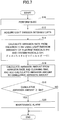
- This process is performed by the controller 100 . Also, in the first example, this process is performed at a time of waferless dry cleaning after a wafer W is unloaded.
- the controller 100 When the process is started, the controller 100 performs the waferless dry cleaning process (step S 10 ). Next, the controller 100 acquires light emission intensity Io of oxygen radicals (O*) and light emission intensity If of fluorine radicals (F*) from the OES 130 (step S 12 ).
- the controller 100 substitutes the acquired light emission intensity Io of the oxygen radicals and the acquired light emission intensity If of the fluorine radicals into Equation (1) to calculate the wastage rate (step S 14 ).
- the controller 100 calculates a wastage amount by multiplying the calculated wastage rate by a processing time of the waferless dry cleaning, and adds the calculated wastage amount to a cumulative wastage amount (sum of wastage amounts having been calculated so far) (step S 16 ).
- the controller 100 determines whether or not the cumulative wastage amount is equal to or larger than the first threshold value Qth (step S 18 ). If it is determined that the cumulative wastage amount is equal to or larger than the first threshold value Qth, the controller 100 outputs a maintenance alarm (step S 20 ), and terminates the process. In contrast, if it is determined that the cumulative wastage amount is less than the first threshold value Qth, the controller 100 terminates the process as is.
- the wastage determination method of the first example it is possible to determine a degree of wastage of a particular expendable part in the processing chamber by calculating an amount of wastage in real time based on light emission intensity measured by the OES 130 , without inhibiting processes of a production wafer. Accordingly, by outputting an alarm such as a maintenance alarm before a defective product is manufactured, replacement of the electrostatic chuck and maintenance can be prompted, generation of a defective product can be suppressed, and a product yield rate can be increased.
- This process is performed by the controller 100 . Also, this process is performed at the time of waferless dry cleaning after the wafer W is unloaded.
- the maintenance alarm is output using a result of comparison of the wastage rate with a second threshold value Rth, in addition to using a result of comparison of the cumulative wastage amount with the first threshold value Qth.
- the second threshold value Rth which is illustrated in the upper part of FIG. 6 , is an example of a wastage limit, and may be preset for each expendable part to be monitored. An alarm may be output when the calculated wastage rate becomes the second threshold value Rth or larger, or when the calculated wastage rate becomes closer to the second threshold value Rth.
- the controller 100 When the process is started, the controller 100 performs the waferless dry cleaning process (step S 10 ). Next, the controller 100 acquires light emission intensity Io of oxygen radicals and light emission intensity If of fluorine radicals from the OES 130 (step S 12 ).
- step S 14 the controller 100 substitutes the acquired light emission intensity Io of the oxygen radicals and the acquired light emission intensity If of the fluorine radicals into Equation (1) to calculate the wastage rate (step S 14 ).
- step S 30 the controller 100 determines whether or not the calculated wastage rate is equal to or larger than the second threshold value Rth (step S 30 ). If it is determined that the calculated wastage rate is equal to or larger than the second threshold value Rth, the controller 100 outputs an alarm of the wastage rate (step S 32 ), and the process proceeds to step S 16 . However, execution of step S 32 may be omitted.
- step S 16 the controller 100 calculates wastage amount by multiplying the calculated wastage rate by a processing time of the waferless dry cleaning, and adds the calculated wastage amount to a cumulative wastage amount (step S 16 ).
- the controller 100 determines whether or not the cumulative wastage amount is equal to or larger than the first threshold value Qth (step S 18 ). If it is determined that the cumulative wastage amount is equal to or larger than the first threshold value Qth, the controller 100 determines whether or not damage intensity is high (step S 34 ). As an example of determining whether or not the damage intensity is high, it may be determined that the damage intensity is high in a case in which the wastage rate is equal to or larger than the second threshold value Rth and in which the cumulative wastage amount is equal to or larger than the first threshold value Qth.
- step S 20 the controller 100 outputs a maintenance alarm
- step S 36 the controller 100 outputs an alarm of the wastage amount
- the wastage determination method of the second example based on a result of comparison of the calculated wastage amount with the first threshold value Qth and a result of comparison of the calculated wastage rate with the second threshold value Rth, degree of wastage of a particular expendable part can be determined.
- the wastage determination method of the second example similarly, it is possible to determine the degree of wastage of a particular expendable part in the processing chamber by calculating the amount of wastage in real time based on the light emission intensity measured by the OES 130 . Therefore, by outputting an alarm such as a maintenance alarm before a defective product is manufactured, replacement of the electrostatic chuck and maintenance can be prompted, generation of defective products can be reduced, and a product yield rate can be increased.
- a time for waterless dry cleaning and the like may often vary depending on a sample structure and the like.
- a wastage state can be accurately recognized. Therefore, by outputting an alarm before a defective product is manufactured, replacement of the electrostatic chuck and maintenance can be performed, and a product yield rate can be increased.
- the wastage determination method and the plasma processing apparatus have been described in accordance with the above-described embodiments, the wastage determination method and the plasma processing apparatus according to the present invention are not limited to the above-described embodiments, and various modifications and enhancements can be made within the scope of the present invention. Matters described in the above-described embodiments may be combined to the extent that they are consistent.
- the controller 100 calculates all of the wastage rate during cleaning, the wastage rate during etching, and the wastage rate during deposition using Equation (1).
- a wastage rate V 1 at a time of cleaning a wastage rate V 2 at a time of etching
- a wastage rate V 3 at a time of deposition may be calculated separately.
- coefficients A, B, and C of Equation (1) for calculating the wastage rate V 1 for cleaning are learned to reflect a degree of wastage of a member during cleaning.
- coefficients A, B, and C of Equation (1) for calculating the wastage rate V 2 for etching are learned to reflect a degree of wastage of a member during etching.
- coefficients A, B, and C of Equation (1) for calculating the wastage rate V 3 for deposition are learned to reflect a degree of wastage of a member during deposition.
- the present invention is applicable not only to a parallel-flat plate type dual-frequency apparatus illustrated in FIG. 1 , but also to other types of plasma processing apparatuses.
- Examples of other types of plasma processing apparatuses may include a capacitively coupled plasma (CCP) type processing apparatus, an inductively coupled plasma (ICP) type processing apparatus, a plasma processing apparatus using a radial line slot antenna, a helicon wave plasma (HWP) type processing apparatus, an electron cyclotron resonance plasma (ECR) type processing apparatus, and a surface wave plasma processing apparatus.
- CCP capacitively coupled plasma
- ICP inductively coupled plasma
- HWP helicon wave plasma
- ECR electron cyclotron resonance plasma
- a substrate to be etched may include various substrates used in an LCD (Liquid Crystal Display), an FPD (Flat Panel Display), and the like, a photomask, a CD substrate, and a printed circuit board.
Landscapes
- Chemical & Material Sciences (AREA)
- Physics & Mathematics (AREA)
- Engineering & Computer Science (AREA)
- Analytical Chemistry (AREA)
- Plasma & Fusion (AREA)
- General Physics & Mathematics (AREA)
- Pathology (AREA)
- Life Sciences & Earth Sciences (AREA)
- Biochemistry (AREA)
- General Health & Medical Sciences (AREA)
- Health & Medical Sciences (AREA)
- Immunology (AREA)
- Dispersion Chemistry (AREA)
- Spectroscopy & Molecular Physics (AREA)
- Organic Chemistry (AREA)
- Drying Of Semiconductors (AREA)
- Condensed Matter Physics & Semiconductors (AREA)
- Manufacturing & Machinery (AREA)
- Computer Hardware Design (AREA)
- Microelectronics & Electronic Packaging (AREA)
- Power Engineering (AREA)
- Chemical Kinetics & Catalysis (AREA)
- General Chemical & Material Sciences (AREA)
- Inorganic Chemistry (AREA)
Abstract
Description
V=A×Io+B×If+C×Io×If (1)
where V is a wastage rate of a particular expendable part, Io is light emission intensity of oxygen radicals, If is light emission intensity of fluorine radicals, and A, B, and C are coefficients.
Claims (16)
V=A×Io+B×If+C×Io×If (1)
Priority Applications (1)
| Application Number | Priority Date | Filing Date | Title |
|---|---|---|---|
| US16/935,418 US11183374B2 (en) | 2016-12-26 | 2020-07-22 | Wastage determination method and plasma processing apparatus |
Applications Claiming Priority (5)
| Application Number | Priority Date | Filing Date | Title |
|---|---|---|---|
| JP2016-251571 | 2016-12-26 | ||
| JP2016251571A JP2018107264A (en) | 2016-12-26 | 2016-12-26 | Consumption determination method and plasma processing apparatus |
| PCT/JP2017/044933 WO2018123621A1 (en) | 2016-12-26 | 2017-12-14 | Consumption determination method and plasma processing device |
| US201916472339A | 2019-06-21 | 2019-06-21 | |
| US16/935,418 US11183374B2 (en) | 2016-12-26 | 2020-07-22 | Wastage determination method and plasma processing apparatus |
Related Parent Applications (2)
| Application Number | Title | Priority Date | Filing Date |
|---|---|---|---|
| US16/472,339 Continuation US10763089B2 (en) | 2016-12-26 | 2017-12-14 | Wastage determination method and plasma processing apparatus |
| PCT/JP2017/044933 Continuation WO2018123621A1 (en) | 2016-12-26 | 2017-12-14 | Consumption determination method and plasma processing device |
Publications (2)
| Publication Number | Publication Date |
|---|---|
| US20200350148A1 US20200350148A1 (en) | 2020-11-05 |
| US11183374B2 true US11183374B2 (en) | 2021-11-23 |
Family
ID=62707351
Family Applications (2)
| Application Number | Title | Priority Date | Filing Date |
|---|---|---|---|
| US16/472,339 Active US10763089B2 (en) | 2016-12-26 | 2017-12-14 | Wastage determination method and plasma processing apparatus |
| US16/935,418 Active US11183374B2 (en) | 2016-12-26 | 2020-07-22 | Wastage determination method and plasma processing apparatus |
Family Applications Before (1)
| Application Number | Title | Priority Date | Filing Date |
|---|---|---|---|
| US16/472,339 Active US10763089B2 (en) | 2016-12-26 | 2017-12-14 | Wastage determination method and plasma processing apparatus |
Country Status (5)
| Country | Link |
|---|---|
| US (2) | US10763089B2 (en) |
| JP (1) | JP2018107264A (en) |
| KR (2) | KR102541742B1 (en) |
| TW (1) | TWI756326B (en) |
| WO (1) | WO2018123621A1 (en) |
Families Citing this family (2)
| Publication number | Priority date | Publication date | Assignee | Title |
|---|---|---|---|---|
| JP7365878B2 (en) | 2019-12-06 | 2023-10-20 | 東京エレクトロン株式会社 | Measuring device and method |
| JP2021144832A (en) * | 2020-03-11 | 2021-09-24 | 東京エレクトロン株式会社 | Plasma measuring device and plasma measuring method |
Citations (3)
| Publication number | Priority date | Publication date | Assignee | Title |
|---|---|---|---|---|
| US7202946B2 (en) * | 2000-11-29 | 2007-04-10 | Lightwind Corporation | Method and device utilizing plasma source for real-time gas sampling |
| JP2011108816A (en) | 2009-11-17 | 2011-06-02 | Tokyo Electron Ltd | Substrate mounting table of substrate processing apparatus |
| JP2016028448A (en) | 2015-10-22 | 2016-02-25 | 東京エレクトロン株式会社 | Installation table, plasma processing device and method for manufacturing installation table |
Family Cites Families (12)
| Publication number | Priority date | Publication date | Assignee | Title |
|---|---|---|---|---|
| US6443165B1 (en) * | 1996-11-14 | 2002-09-03 | Tokyo Electron Limited | Method for cleaning plasma treatment device and plasma treatment system |
| JP4554037B2 (en) * | 2000-07-04 | 2010-09-29 | 東京エレクトロン株式会社 | Consumable consumption level prediction method and deposited film thickness prediction method |
| WO2002090615A1 (en) * | 2001-05-04 | 2002-11-14 | Lam Research Corporation | Duo-step plasma cleaning of chamber residues |
| JP4033730B2 (en) * | 2002-07-10 | 2008-01-16 | 東京エレクトロン株式会社 | Substrate mounting table for plasma processing apparatus, plasma processing apparatus, and base for plasma processing apparatus |
| JP2004237321A (en) * | 2003-02-06 | 2004-08-26 | Komatsu Sanki Kk | Plasma processing device |
| US7959970B2 (en) * | 2004-03-31 | 2011-06-14 | Tokyo Electron Limited | System and method of removing chamber residues from a plasma processing system in a dry cleaning process |
| JP4707421B2 (en) * | 2005-03-14 | 2011-06-22 | 東京エレクトロン株式会社 | Processing apparatus, consumable part management method for processing apparatus, processing system, and consumable part management method for processing system |
| JP4620524B2 (en) * | 2005-05-17 | 2011-01-26 | 株式会社日立ハイテクノロジーズ | Plasma processing equipment |
| JP2011060977A (en) * | 2009-09-09 | 2011-03-24 | Toshiba Corp | Manufacturing apparatus of semiconductor device and manufacturing method |
| JP2011210853A (en) * | 2010-03-29 | 2011-10-20 | Tokyo Electron Ltd | Method for measuring wear rate |
| KR101877862B1 (en) * | 2014-12-19 | 2018-07-12 | 가부시키가이샤 히다치 하이테크놀로지즈 | Plasma processing apparatus and driving method thereof |
| US10041868B2 (en) * | 2015-01-28 | 2018-08-07 | Lam Research Corporation | Estimation of lifetime remaining for a consumable-part in a semiconductor manufacturing chamber |
-
2016
- 2016-12-26 JP JP2016251571A patent/JP2018107264A/en active Pending
-
2017
- 2017-12-14 KR KR1020227025105A patent/KR102541742B1/en active Active
- 2017-12-14 KR KR1020197017207A patent/KR102424651B1/en active Active
- 2017-12-14 US US16/472,339 patent/US10763089B2/en active Active
- 2017-12-14 WO PCT/JP2017/044933 patent/WO2018123621A1/en not_active Ceased
- 2017-12-18 TW TW106144345A patent/TWI756326B/en active
-
2020
- 2020-07-22 US US16/935,418 patent/US11183374B2/en active Active
Patent Citations (3)
| Publication number | Priority date | Publication date | Assignee | Title |
|---|---|---|---|---|
| US7202946B2 (en) * | 2000-11-29 | 2007-04-10 | Lightwind Corporation | Method and device utilizing plasma source for real-time gas sampling |
| JP2011108816A (en) | 2009-11-17 | 2011-06-02 | Tokyo Electron Ltd | Substrate mounting table of substrate processing apparatus |
| JP2016028448A (en) | 2015-10-22 | 2016-02-25 | 東京エレクトロン株式会社 | Installation table, plasma processing device and method for manufacturing installation table |
Also Published As
| Publication number | Publication date |
|---|---|
| WO2018123621A1 (en) | 2018-07-05 |
| KR20190098143A (en) | 2019-08-21 |
| US20200350148A1 (en) | 2020-11-05 |
| KR102424651B1 (en) | 2022-07-25 |
| US20190378698A1 (en) | 2019-12-12 |
| KR20220106859A (en) | 2022-07-29 |
| TW201831052A (en) | 2018-08-16 |
| US10763089B2 (en) | 2020-09-01 |
| KR102541742B1 (en) | 2023-06-13 |
| JP2018107264A (en) | 2018-07-05 |
| TWI756326B (en) | 2022-03-01 |
Similar Documents
| Publication | Publication Date | Title |
|---|---|---|
| JP4884047B2 (en) | Plasma processing method | |
| CN106468541B (en) | The abrasion detection of consumable part in semiconductor manufacturing facility | |
| JP6661283B2 (en) | Cleaning method and plasma processing method | |
| US9117769B2 (en) | Plasma etching method | |
| US8999068B2 (en) | Chamber cleaning method | |
| KR101720670B1 (en) | Substrate processing apparatus, cleaning method thereof and storage medium storing program | |
| US7959970B2 (en) | System and method of removing chamber residues from a plasma processing system in a dry cleaning process | |
| US10770268B2 (en) | Plasma processing method and plasma processing apparatus | |
| US20070224709A1 (en) | Plasma processing method and apparatus, control program and storage medium | |
| US9147556B2 (en) | Plasma processing method and plasma processing apparatus | |
| TW201916098A (en) | Plasma processing device and wet cleaning method | |
| KR102810904B1 (en) | In-situ real-time plasma chamber condition monitoring | |
| US20110049098A1 (en) | Plasma etching method | |
| JP2016225567A (en) | Cleaning method | |
| JP4828456B2 (en) | Plasma processing method and plasma processing apparatus | |
| US11183374B2 (en) | Wastage determination method and plasma processing apparatus | |
| WO2009110366A1 (en) | Plasma processing apparatus | |
| US9925571B2 (en) | Method of cleaning substrate processing apparatus | |
| US20080257863A1 (en) | Plasma processing apparatus and method for stabilizing inner wall of processing chamber | |
| US8328981B2 (en) | Method for heating a focus ring in a plasma apparatus by high frequency power while no plasma being generated | |
| CN114823269B (en) | Abnormality detection method for plasma processing device and plasma processing device | |
| KR20230119605A (en) | Substrate processing method and substrate processing apparatus | |
| JP2009260091A (en) | Seasoning method of plasma treatment device |
Legal Events
| Date | Code | Title | Description |
|---|---|---|---|
| AS | Assignment |
Owner name: TOKYO ELECTRON LIMITED, JAPAN Free format text: ASSIGNMENT OF ASSIGNORS INTEREST;ASSIGNORS:KUSANO, SHU;HIRAYAMA, YUSUKE;REEL/FRAME:053277/0246 Effective date: 20190619 |
|
| FEPP | Fee payment procedure |
Free format text: ENTITY STATUS SET TO UNDISCOUNTED (ORIGINAL EVENT CODE: BIG.); ENTITY STATUS OF PATENT OWNER: LARGE ENTITY |
|
| STPP | Information on status: patent application and granting procedure in general |
Free format text: DOCKETED NEW CASE - READY FOR EXAMINATION |
|
| STPP | Information on status: patent application and granting procedure in general |
Free format text: NON FINAL ACTION MAILED |
|
| STPP | Information on status: patent application and granting procedure in general |
Free format text: NOTICE OF ALLOWANCE MAILED -- APPLICATION RECEIVED IN OFFICE OF PUBLICATIONS |
|
| STPP | Information on status: patent application and granting procedure in general |
Free format text: PUBLICATIONS -- ISSUE FEE PAYMENT VERIFIED |
|
| STCF | Information on status: patent grant |
Free format text: PATENTED CASE |
|
| MAFP | Maintenance fee payment |
Free format text: PAYMENT OF MAINTENANCE FEE, 4TH YEAR, LARGE ENTITY (ORIGINAL EVENT CODE: M1551); ENTITY STATUS OF PATENT OWNER: LARGE ENTITY Year of fee payment: 4 |