US11171237B2 - Middle of line gate structures - Google Patents
Middle of line gate structures Download PDFInfo
- Publication number
- US11171237B2 US11171237B2 US16/386,902 US201916386902A US11171237B2 US 11171237 B2 US11171237 B2 US 11171237B2 US 201916386902 A US201916386902 A US 201916386902A US 11171237 B2 US11171237 B2 US 11171237B2
- Authority
- US
- United States
- Prior art keywords
- gate
- structures
- gate structure
- source
- bridged
- Prior art date
- Legal status (The legal status is an assumption and is not a legal conclusion. Google has not performed a legal analysis and makes no representation as to the accuracy of the status listed.)
- Active, expires
Links
Images


Classifications
-
- H—ELECTRICITY
- H10—SEMICONDUCTOR DEVICES; ELECTRIC SOLID-STATE DEVICES NOT OTHERWISE PROVIDED FOR
- H10D—INORGANIC ELECTRIC SEMICONDUCTOR DEVICES
- H10D30/00—Field-effect transistors [FET]
- H10D30/60—Insulated-gate field-effect transistors [IGFET]
- H10D30/62—Fin field-effect transistors [FinFET]
-
- H01L29/785—
-
- H—ELECTRICITY
- H10—SEMICONDUCTOR DEVICES; ELECTRIC SOLID-STATE DEVICES NOT OTHERWISE PROVIDED FOR
- H10D—INORGANIC ELECTRIC SEMICONDUCTOR DEVICES
- H10D84/00—Integrated devices formed in or on semiconductor substrates that comprise only semiconducting layers, e.g. on Si wafers or on GaAs-on-Si wafers
- H10D84/01—Manufacture or treatment
- H10D84/0123—Integrating together multiple components covered by H10D12/00 or H10D30/00, e.g. integrating multiple IGBTs
- H10D84/0126—Integrating together multiple components covered by H10D12/00 or H10D30/00, e.g. integrating multiple IGBTs the components including insulated gates, e.g. IGFETs
- H10D84/0158—Integrating together multiple components covered by H10D12/00 or H10D30/00, e.g. integrating multiple IGBTs the components including insulated gates, e.g. IGFETs the components including FinFETs
-
- H01L21/823437—
-
- H01L21/823821—
-
- H01L29/66545—
-
- H01L29/66795—
-
- H—ELECTRICITY
- H10—SEMICONDUCTOR DEVICES; ELECTRIC SOLID-STATE DEVICES NOT OTHERWISE PROVIDED FOR
- H10D—INORGANIC ELECTRIC SEMICONDUCTOR DEVICES
- H10D30/00—Field-effect transistors [FET]
- H10D30/01—Manufacture or treatment
- H10D30/021—Manufacture or treatment of FETs having insulated gates [IGFET]
- H10D30/024—Manufacture or treatment of FETs having insulated gates [IGFET] of fin field-effect transistors [FinFET]
-
- H—ELECTRICITY
- H10—SEMICONDUCTOR DEVICES; ELECTRIC SOLID-STATE DEVICES NOT OTHERWISE PROVIDED FOR
- H10D—INORGANIC ELECTRIC SEMICONDUCTOR DEVICES
- H10D64/00—Electrodes of devices having potential barriers
- H10D64/01—Manufacture or treatment
- H10D64/017—Manufacture or treatment using dummy gates in processes wherein at least parts of the final gates are self-aligned to the dummy gates, i.e. replacement gate processes
-
- H—ELECTRICITY
- H10—SEMICONDUCTOR DEVICES; ELECTRIC SOLID-STATE DEVICES NOT OTHERWISE PROVIDED FOR
- H10D—INORGANIC ELECTRIC SEMICONDUCTOR DEVICES
- H10D84/00—Integrated devices formed in or on semiconductor substrates that comprise only semiconducting layers, e.g. on Si wafers or on GaAs-on-Si wafers
- H10D84/01—Manufacture or treatment
- H10D84/0123—Integrating together multiple components covered by H10D12/00 or H10D30/00, e.g. integrating multiple IGBTs
- H10D84/0126—Integrating together multiple components covered by H10D12/00 or H10D30/00, e.g. integrating multiple IGBTs the components including insulated gates, e.g. IGFETs
- H10D84/0135—Manufacturing their gate conductors
-
- H—ELECTRICITY
- H10—SEMICONDUCTOR DEVICES; ELECTRIC SOLID-STATE DEVICES NOT OTHERWISE PROVIDED FOR
- H10D—INORGANIC ELECTRIC SEMICONDUCTOR DEVICES
- H10D84/00—Integrated devices formed in or on semiconductor substrates that comprise only semiconducting layers, e.g. on Si wafers or on GaAs-on-Si wafers
- H10D84/01—Manufacture or treatment
- H10D84/0123—Integrating together multiple components covered by H10D12/00 or H10D30/00, e.g. integrating multiple IGBTs
- H10D84/0126—Integrating together multiple components covered by H10D12/00 or H10D30/00, e.g. integrating multiple IGBTs the components including insulated gates, e.g. IGFETs
- H10D84/0165—Integrating together multiple components covered by H10D12/00 or H10D30/00, e.g. integrating multiple IGBTs the components including insulated gates, e.g. IGFETs the components including complementary IGFETs, e.g. CMOS devices
- H10D84/0193—Integrating together multiple components covered by H10D12/00 or H10D30/00, e.g. integrating multiple IGBTs the components including insulated gates, e.g. IGFETs the components including complementary IGFETs, e.g. CMOS devices the components including FinFETs
-
- H—ELECTRICITY
- H10—SEMICONDUCTOR DEVICES; ELECTRIC SOLID-STATE DEVICES NOT OTHERWISE PROVIDED FOR
- H10D—INORGANIC ELECTRIC SEMICONDUCTOR DEVICES
- H10D84/00—Integrated devices formed in or on semiconductor substrates that comprise only semiconducting layers, e.g. on Si wafers or on GaAs-on-Si wafers
- H10D84/01—Manufacture or treatment
- H10D84/02—Manufacture or treatment characterised by using material-based technologies
- H10D84/03—Manufacture or treatment characterised by using material-based technologies using Group IV technology, e.g. silicon technology or silicon-carbide [SiC] technology
- H10D84/038—Manufacture or treatment characterised by using material-based technologies using Group IV technology, e.g. silicon technology or silicon-carbide [SiC] technology using silicon technology, e.g. SiGe
-
- H—ELECTRICITY
- H10—SEMICONDUCTOR DEVICES; ELECTRIC SOLID-STATE DEVICES NOT OTHERWISE PROVIDED FOR
- H10D—INORGANIC ELECTRIC SEMICONDUCTOR DEVICES
- H10D84/00—Integrated devices formed in or on semiconductor substrates that comprise only semiconducting layers, e.g. on Si wafers or on GaAs-on-Si wafers
- H10D84/80—Integrated devices formed in or on semiconductor substrates that comprise only semiconducting layers, e.g. on Si wafers or on GaAs-on-Si wafers characterised by the integration of at least one component covered by groups H10D12/00 or H10D30/00, e.g. integration of IGFETs
- H10D84/82—Integrated devices formed in or on semiconductor substrates that comprise only semiconducting layers, e.g. on Si wafers or on GaAs-on-Si wafers characterised by the integration of at least one component covered by groups H10D12/00 or H10D30/00, e.g. integration of IGFETs of only field-effect components
- H10D84/83—Integrated devices formed in or on semiconductor substrates that comprise only semiconducting layers, e.g. on Si wafers or on GaAs-on-Si wafers characterised by the integration of at least one component covered by groups H10D12/00 or H10D30/00, e.g. integration of IGFETs of only field-effect components of only insulated-gate FETs [IGFET]
- H10D84/834—Integrated devices formed in or on semiconductor substrates that comprise only semiconducting layers, e.g. on Si wafers or on GaAs-on-Si wafers characterised by the integration of at least one component covered by groups H10D12/00 or H10D30/00, e.g. integration of IGFETs of only field-effect components of only insulated-gate FETs [IGFET] comprising FinFETs
-
- H—ELECTRICITY
- H10—SEMICONDUCTOR DEVICES; ELECTRIC SOLID-STATE DEVICES NOT OTHERWISE PROVIDED FOR
- H10D—INORGANIC ELECTRIC SEMICONDUCTOR DEVICES
- H10D84/00—Integrated devices formed in or on semiconductor substrates that comprise only semiconducting layers, e.g. on Si wafers or on GaAs-on-Si wafers
- H10D84/01—Manufacture or treatment
- H10D84/0123—Integrating together multiple components covered by H10D12/00 or H10D30/00, e.g. integrating multiple IGBTs
- H10D84/0126—Integrating together multiple components covered by H10D12/00 or H10D30/00, e.g. integrating multiple IGBTs the components including insulated gates, e.g. IGFETs
- H10D84/0149—Manufacturing their interconnections or electrodes, e.g. source or drain electrodes
Definitions
- the present disclosure generally relates to semiconductor structures and, more particularly, to middle of line gate structures and methods of manufacture.
- MOL middle of line
- gate contacts can connect adjacent gate structures with respect to one another.
- these gate contacts require a relatively minimal size due to a lack of real estate.
- fabrication of these gate contacts requires a relatively limited process margin and inline process control in order to prevent shorting between the gate contacts and source and drain metallization features.
- the size and shape of these source and drain metallization features are limited by current MOL structures.
- a structure comprises: a plurality of adjacent gate structures; a bridged gate structure composed of a plurality of the adjacent gate structures; source and drain regions adjacent to the bridged gate structure and comprising source and drain metallization features; and contacts to the bridged gate structure and the source and drain metallization features.
- a structure comprises: a plurality of gate structures comprising source/drain regions, gate materials, sidewall spacers and a capping material on the gate materials; a bridge structure spanning between two or more gate structures of the plurality of gate structures; a plurality of source and drain metallization features in electrical contact with the source/drain regions; and a contact on the bridge structure.
- a method comprises: forming a plurality of gate structures; bridging the gate structures to form a bridged gate structure; and forming a contact to the bridged gate structure.
- FIGS. 1A-1E show the formation of dummy gate structures, amongst other features, and respective fabrication processes in accordance with aspects of the present disclosure.
- FIGS. 2A-2D show cross-sectional views of the dummy gate structures, amongst other features, and respective fabrication processes in accordance with aspects of the present disclosure.
- FIGS. 3A-3C show cross-sectional views of replacement gate structures, amongst other features, and respective fabrication processes in accordance with aspects of the present disclosure.
- FIGS. 4A-4D show cross-sectional views of source/drain and gate contacts, amongst other features, and respective fabrication processes in accordance with aspects of the present disclosure.
- FIGS. 5A and 5B show respective structures and fabrication processes in accordance with alternative aspects of the present disclosure.
- the present disclosure generally relates to semiconductor structures and, more particularly, to middle of line gate structures and methods of manufacture.
- the processes and structures provided herein allow for the formation of a bridged gate structure by bridging together adjacent gate structures.
- the bridged gate structure allows for a relatively significant reduction in gate contact sizing. Accordingly, a middle of line (MOL) multi-finger (multi-fin) device with a single gate contact can be achieved.
- MOL middle of line
- the reduced gate contact of the bridged gate structure allows for scaling in MOL structures and also for enlargement of an MOL process margin. Additionally, the reduced gate contact allows for adjacent source and drain (S/D) metallization features to have greater flexibility with respect to sizes, shapes and placement, e.g., a single S/D metallization feature spanning the fin structures. This flexibility with respect to the S/D metallization features allows for a reduction in process steps and materials, i.e., less patterning steps, along with an increase in the process margin because of the elimination of a risk for shorting between the gate contact and the S/D metallization features provided by the bridged gate structure.
- S/D source and drain
- the structures and processes described herein provide for a method to form a bridged gate structure having a reduced gate contact.
- the method includes: a relatively narrow gate hard mask; a relatively wide gate hard mask; a gate connect hard mask; patterning of the hardmasks; dummy gate formation; replacement gate formation; and formation of contacts to bridged gate structures.
- the structures and processes described herein allow for a bridged gate structure to have a reduced gate contact area.
- the bridged gate structure includes the following features: an “H” shaped bridged gate structure; a relatively smaller gate contact; and optimized source and drain metallization features, amongst other features.
- the structures of the present disclosure can be manufactured in a number of ways using a number of different tools.
- the methodologies and tools are used to form structures with dimensions in the micrometer and nanometer scale.
- the methodologies, i.e., technologies, employed to manufacture the structure of the present disclosure have been adopted from integrated circuit (IC) technology.
- the structures are built on wafers and are realized in films of material patterned by photolithographic processes on the top of a wafer.
- the fabrication of the structure uses three basic building blocks: (i) deposition of thin films of material on a substrate, (ii) applying a patterned mask on top of the films by photolithographic imaging, and (iii) etching the films selectively to the mask.
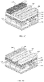
- FIGS. 1A-1E show an incoming structure and respective fabrication processes in accordance with aspects of the present disclosure. More specifically, FIG. 1A shows a structure 100 comprising a substrate 110 composed of a suitable semiconductor material.
- the substrate 110 may be composed of any suitable material including, but not limited to, Si, SiGe, SiGeC, SiC, GaAs, InAs, InP, etc.
- the substrate 110 is used to form fin structures 120 .
- the fin structures 120 can be fabricated using a sidewall image transfer (SIT) technique.
- SIT sidewall image transfer
- a mandrel material e.g., SiO 2
- CVD chemical vapor deposition
- a resist is formed on the mandrel material, and exposed to light to form a pattern (openings).
- a reactive ion etching (RIE) is performed through the openings to form the mandrels.
- the mandrels can have different widths and/or spacing depending on the desired dimensions of the fin structures 120 .
- Spacers are formed on the sidewalls of the mandrels which are preferably material that is different than the mandrels, and which are formed using conventional deposition processes known to those of skill in the art.
- the spacers can have a width which matches the dimensions of the fin structures 120 , for example.
- the mandrels are removed or stripped using a conventional etching process, selective to the mandrel material. An etching is then performed within the spacing of the spacers to form the sub-lithographic features.
- the sidewall spacers can then be stripped.
- An insulator material 125 is deposited on and over the fin structures 120 by a CVD process.
- a poly Si material 130 is deposited over the substrate 110 and the fin structures 120 .
- the poly Si material 130 can be deposited by CVD processes, followed by a conventional chemical mechanical polishing (CMP) process.
- a capping layer 140 is deposited on the poly Si material 130 .
- the capping layer 140 can be a nitride material, e.g., SiN, deposited by CVD processes.
- a hardmask material 150 is formed on the capping layer 140 .
- the hardmask material 150 can be a material which has a different patterning selectivity to the poly Si material 130 and the capping layer 140 .
- the hardmask material 150 is deposited by CVD processes.
- a patterned hardmask structure 160 is formed on the hardmask material 150 .
- the patterned hardmask structure 160 can be formed by a sidewall-assisted double patterning (SADP) process as is known to those of skill in the art such that no further explanation is needed.
- SADP sidewall-assisted double patterning
- the patterned hardmask structure 160 can be comprised of a material having a different selectivity compared to the poly Si material 130 , the capping layer 140 and the hardmask material 150 . As shown, the patterned hardmask structure 160 is patterned into strips on a single side of the structure 100 .
- FIG. 1B shows an oxide layer 170 on the patterned hardmask structure 160 and over the hardmask material 150 .
- the oxide layer 170 can be composed of SOH, amongst other examples, and is deposited by any conventional deposition processes, e.g., CVD processes.
- Patterned hardmasks 180 , 190 are formed on the oxide layer 170 and are comprised of a nitride material, e.g., SiN.
- the patterned hardmask 190 is used to pattern a hardmask for a local gate connection between adjacent gate structures formed using the patterned hardmask structure 160 ; whereas patterned hardmask 180 allows for separate gate structures to be formed.
- the patterned hardmasks 180 , 190 are patterned using conventional lithography and etching processes known to those of ordinary skill in the art such that no further explanation is required for a complete understanding of the disclosure.
- an etching process with a selective chemistry e.g., a RIE process will be used along with the patterned hardmask structures 180 , 190 to form the patterned hardmask structures 200 , 210 .
- the patterned hardmask structures 200 are patterned on the underlying hardmask material 150 , with patterned hardmask 210 spanning between adjacent patterned hardmask structures 160 .
- the patterned hardmask structures 180 , 190 can be stripped by conventional stripping processes.
- a further etching process with a selective chemistry e.g., RIE process, will be used with the patterned hardmask structures 160 , 200 , 210 to form the patterned hardmask structures 220 , 230 , 240 .
- the patterned hardmask structure 240 is between adjacent patterned hardmask structures 230 .
- the structures 160 , 200 , 210 can be stripped by conventional stripping processes.
- FIG. 1E shows the formation of dummy gate structures 250 , 260 , and particularly bridged dummy gate structure 260 a formed from the dummy gate structures 260 .
- the dummy gate structures 250 , 260 are formed using a RIE process which is selective to the poly Si material 130 and the capping layer 140 .
- the hardmask structure 240 forms a local dummy gate connection (bridged) 270 , which connects adjacent gate structures of the dummy gate structures 260 ; that is, select dummy gate structures 260 are cladded or bridged together by the dummy gate connection 270 to form the bridged dummy gate structure 260 a.
- the bridged dummy gate structure 260 a can be an “H” shaped gate structure; however, other shapes are contemplated herein depending on the shape, size and/or position of the dummy gate connection 270 , e.g., a “U” shaped bridged gate structure, amongst other examples.
- the bridged dummy gate structure 260 a can comprise at least two dummy gate structures 260 bridged (cladded) together; however, any number of dummy gate structures 260 can be bridged together to form the bridged dummy gate structure 260 a.
- the dummy gate structures 250 are relatively wider than the dummy gate structures 260 .
- the dummy gate structures 260 can have a width in a range of about 5 nm to 40 nm, while the dummy gate structures 250 can have a width in a range of about 80 nm to 250 nm.
- the dummy gate structures 260 may be wider than the dummy gate structures 250 , or that the dummy gate structures 250 , 260 may have the same width.
- the fin structures 120 partially extend through a top surface of the insulator material 125 . In this way, the fin structures 120 are partially exposed.
- FIGS. 2A-2D illustrate the dummy gate structures 260 , 260 a .
- FIG. 2A shows a top view of the dummy gate structures 260 , 260 a ; whereas FIG. 2B shows a cross-sectional view in an X1-axis direction for the dummy gate structures 260 , 260 a .
- FIG. 2C shows a cross-sectional view in an X2-axis direction and FIG. 2D shows a cross-sectional view in a Y-axis direction for the dummy gate structures 260 , 260 a .
- FIGS. 2A-2D show sidewall spacers 280 , e.g., a low-k dielectric, deposited on the sidewalls of the dummy gate structures 260 , 260 a , i.e., the poly Si material 130 .
- the sidewall spacers 280 can be deposited by conventional CVD processes followed by a patterning process, e.g., anisotropic etching process, to remove any material from horizontal surfaces of the fin structures 120 and the poly Si material 130 .
- FIGS. 2C and 2D show the insulator layer 125 which forms isolation regions (shallow trench isolation regions) adjacent to the dummy gate structures 260 , 260 a and between the fin structures 120 .
- FIGS. 3A-3C show replacement gate structures 310 , 310 a in accordance with aspects of the disclosure.
- source and drain (S/D) regions 300 are formed on the sides of the gate structures 310 , 310 a in the substrate 110 of the fin structures 120 using, e.g., any conventional doping/ion implementation process.
- the S/D regions 300 can be formed by an ion implantation process, doping process or through a diffusion process, as is well known to those of skill in the art such that no further explanation is required for an understanding of the present disclosure.
- the S/D regions 300 can be raised S/D regions 300 formed by an epi growth on the surfaces of the substrate 110 between the dummy gate structures 260 , 260 a , as shown in FIGS. 3A and 3C .
- the gate structures 310 , 310 a are formed in trenches, which are formed by the removal of the poly Si material 130 of the dummy gate structures 260 , 260 a , using conventional lithography and etching techniques, e.g., a RIE process. For example, an etching process will be used to remove the poly Si material 130 to form one or more trenches between the sidewall spacers 280 .
- Gate structures 310 , 310 a are formed within the trenches on the fin structures 120 by replacement gate fabrication processes.
- the gate structures 310 can have a width in a range of about 5 nm to 40 nm, or a width in a range of about 80 nm to 250 nm, amongst other examples.
- the gate structures 310 , 310 a include a gate dielectric 320 and metallization features 330 , 340 .
- the gate dielectric 320 can be, e.g., a high-k gate dielectric material, e.g., hafnium-based dielectrics.
- the high-k dielectric materials can include, but are not limited to: Al 2 O 3 , Ta 2 O 3 , TiO 2 , La 2 O 3 , SrTiO 3 , LaAlO 3 , ZrO 2 , Y 2 O 3 , Gd 2 O 3 , and combinations including multilayers thereof.
- the gate metallization feature i.e., workfunction metal 330
- the workfunction metal 330 can be a tungsten (W) material.
- the remaining metallization feature, i.e., gate metal 340 can include any conductive material, e.g., TiN, TaN, amongst other examples.
- a capping material 350 is deposited over the gate dielectric 320 and the gate metallization features 330 , 340 , by CVD processes, followed by a CMP process. Accordingly, the plurality of adjacent gate structures 310 are finFET gate structures.
- the gate structures 310 comprise adjacent gate structures 310 which are bridged together by a gate connection. Specifically, the poly Si material 130 of the bridged dummy gate structure 260 a is replaced with the gate materials 320 , 330 , 340 . Further, the connection established by the dummy gate connection 270 of FIG. 2A remains during the replacement gate process. In this way, during the replacement gate process, the replacement gate structure is a bridged gate structure 310 a because of the previous gate connection established by dummy gate connection 270 .
- the gate materials 320 , 330 , 340 will be shared between the adjacent gate structures 310 in the bridged gate structure 310 a .
- the bridged gate structure 310 a comprises a bridge between two adjacent gate structures 310 , comprised of a conductive gate material, i.e., workfunction metal 330 and gate metal 340 .
- the bridge structure provides electrical contact between gate material of the two or more gate structures.
- the bridge structure i.e., bridged gate structure 310 a , comprises a gate dielectric 320 , a workfunction metal 330 and a gate metal 340 .
- the bridged gate structure 310 a allows for a relatively significant reduction for a subsequent gate contact. In this way, a middle of line (MOL) multi-finger (multi-fin) device with a single gate contact can be achieved with an increased process of margin.
- MOL middle of line
- FIGS. 3A-3C further show source/drain (S/D) metallization features 360 formed in contact with the S/D regions 300 .
- a silicide liner is deposited over the S/D regions 300 which is then subjected to a silicide process.
- a metal material is deposited on the silicide liner, thereby forming the source/drain metallization features 360 .
- the metal material can be composed of cobalt (Co), tungsten (W) or Ruthenium (Ru), for example.
- a dielectric layer 290 is deposited over and between the gate structures 310 , 310 a .
- the dielectric layer 290 is deposited within trenches between the gate structures 310 , 310 a by CVD processes.
- the dielectric layer 290 is an interlevel dielectric material, preferably composed of oxide.
- CMP chemical mechanical planarization
- the bridge gate structure 310 a is an H-shape.
- the bridged gate structure 310 a can be other bridged shapes, e.g., U-shaped.
- FIGS. 4A-4D show S/D contacts 370 and gate contact 380 .
- the S/D contacts 370 and gate contact 380 can be formed together or sequentially.
- Fabrication of the S/D contacts 370 and gate contact 380 includes forming a resist over the dielectric layer 290 , which is exposed to energy (light) to form a pattern (opening).
- An etching process with a selective chemistry, e.g., RIE, will be used to form one or more trenches in the dielectric layer 290 and the capping material 350 through the openings of the resist.
- the resist can be removed by a conventional oxygen ashing process or other known stripants, followed by the deposition of a conductive material by conventional deposition processes, e.g., CVD processes, to form the S/D contacts 370 and gate contact 380 .
- a conductive material e.g., CVD processes
- Any residual conductive material on the surface of the dielectric layer 290 can be removed by conventional chemical mechanical polishing (CMP) processes.
- CMP chemical mechanical polishing
- the gate contact 380 is a reduced gate contact, which allows for scaling in MOL structures and also for enlargement of an MOL process margin without any concern for shorting to occur between the gate structure and the S/D metallization features 360 .
- the bridged gate structure 310 a includes a gate connection 270 a so that the bridged gate structure 310 a is formed on the plurality of adjacent gate structures 310 and the bridged gate structure 310 a .
- the gate connection 270 a allows for the gate contact 380 to be in electrical contact with more than one gate structure 310 will still having a reduced size.
- the gate contact 380 to the bridged gate structure 310 a is positioned within the gate connection 270 a and in electrical contact with the plurality of adjacent gate structures 310 .
- a plurality of gate structures 310 comprising source/drain regions 300 , gate materials 320 , 330 , 340 , sidewall spacers 280 and a capping material 350 on the gate materials 320 , 330 , 340 , is provided herein.
- a bridge structure i.e., bridged gate structure 310 a , spans between two or more gate structures 310 of the plurality of gate structures 310 , and a plurality of source and drain metallization features 360 are in electrical contact with the source/drain regions 300 .
- a contact, i.e., gate contact 380 is on the bridge structure.
- a fill material of the source and drain metallization features 360 is below the contact, i.e., gate contact 380 .
- the structures and processes described herein provide for a plurality of adjacent gate structures 310 , and a bridged gate structure 310 a composed of a plurality of the adjacent gate structures 310 . Further, there are source and drain regions 300 adjacent to the bridged gate structure 310 a and comprising source and drain metallization features 360 . Additionally, the structures and processes described herein provide for contacts 370 , 380 to the bridged gate structure 310 a and the source and drain metallization features 360 .
- FIGS. 5A and 5B show alternative structures and fabrication processes in accordance with the present disclosure.
- FIG. 5A shows a top view of a structure having alternative (S/D) metallization features 360 a .
- S/D metallization features 360 have greater flexibility with respect to sizes, shapes and placement.
- FIG. 4A shows separate S/D metallization features 360 on each fin structure 120 ; whereas FIG. 5A shows a single S/D metallization feature 360 a spanning the fin structures 120 .
- the source and drain metallization features 360 extend across fin structures 120 of the finFET gate structures, i.e., gate structures 310 .
- the contacts i.e., S/D contacts 370
- the source and drain metallization features 360 a which extend to opposing fins 120 .
- the source and drain metallization features 360 a extend alongside the contact, i.e., gate contact 380 .
- FIG. 5B shows a cross-sectional view along X2-axis direction, with the same metal fill used for the S/D metallization features 360 a being deposited directly on the gate metallization features 330 , 340 , as opposed to FIG. 4C where the gate contact 380 is in direct electrical contact with the gate metallization features 330 , 340 .
- the gate connection 270 a allows for the gate contact 380 to be in electrical contact with more than one gate structure 310 will still having a reduced size.
- the structures and processes described herein provide for a method with the steps of: forming a plurality of gate structures 310 ; bridging the gate structures 310 to form a bridged gate structure 310 a ; and forming a contact, i.e., gate contact 380 , to the bridged gate structure 310 a .
- Additional steps include: forming source and drain regions 300 ; forming metallization features 360 a to the source and drain regions 300 which extend alongside the contact, i.e., gate contact 380 ; and forming contacts 370 to the metallization features 360 a by depositing a fill material simultaneously on the source and drain regions 300 and the bridged gate structure 310 a , as illustrated in FIG. 5B .
- the bridging of the gate structures 310 comprises patterning a gate connection 190 , 210 , 240 , 270 over dummy gate structures 160 , 230 , 260 through a plurality of underlying layers 130 , 140 , 150 , 170 .
- the processes and resultant structures described herein allow for the formation of a bridged (cladded) gate structure by bridging adjacent gate structures together.
- the cladded gate structure allows for a relatively significant reduction in gate contact sizing. In this way, a middle of line (MOL) multi-finger (multi-fin) device with a single gate contact can be achieved.
- MOL middle of line
- the reduced gate contact of the bridged gate structure allows for scaling in MOL structures and also for enlargement of an MOL process margin.
- the reduced gate contact allows for adjacent S/D metallization features to have greater flexibility with respect to sizes, shapes and placement, e.g., a single S/D metallization feature spanning the fin structures.
- This flexibility with respect to the S/D metallization features allows for a reduction in process steps and materials, i.e., less patterning steps, along with an increase in the process margin because of the elimination of a risk for shorting between the gate contact and the S/D metallization features provided by the bridged gate structure.
- the method(s) as described above is used in the fabrication of integrated circuit chips.
- the resulting integrated circuit chips can be distributed by the fabricator in raw wafer form (that is, as a single wafer that has multiple unpackaged chips), as a bare die, or in a packaged form.
- the chip is mounted in a single chip package (such as a plastic carrier, with leads that are affixed to a motherboard or other higher level carrier) or in a multichip package (such as a ceramic carrier that has either or both surface interconnections or buried interconnections).
- the chip is then integrated with other chips, discrete circuit elements, and/or other signal processing devices as part of either (a) an intermediate product, such as a motherboard, or (b) an end product.
- the end product can be any product that includes integrated circuit chips, ranging from toys and other low-end applications to advanced computer products having a display, a keyboard or other input device, and a central processor.
Landscapes
- Thin Film Transistor (AREA)
- Electrodes Of Semiconductors (AREA)
Abstract
Description
Claims (19)
Priority Applications (1)
| Application Number | Priority Date | Filing Date | Title |
|---|---|---|---|
| US16/386,902 US11171237B2 (en) | 2019-04-17 | 2019-04-17 | Middle of line gate structures |
Applications Claiming Priority (1)
| Application Number | Priority Date | Filing Date | Title |
|---|---|---|---|
| US16/386,902 US11171237B2 (en) | 2019-04-17 | 2019-04-17 | Middle of line gate structures |
Publications (2)
| Publication Number | Publication Date |
|---|---|
| US20200335619A1 US20200335619A1 (en) | 2020-10-22 |
| US11171237B2 true US11171237B2 (en) | 2021-11-09 |
Family
ID=72830929
Family Applications (1)
| Application Number | Title | Priority Date | Filing Date |
|---|---|---|---|
| US16/386,902 Active 2039-08-09 US11171237B2 (en) | 2019-04-17 | 2019-04-17 | Middle of line gate structures |
Country Status (1)
| Country | Link |
|---|---|
| US (1) | US11171237B2 (en) |
Families Citing this family (1)
| Publication number | Priority date | Publication date | Assignee | Title |
|---|---|---|---|---|
| CN120076304B (en) * | 2023-11-22 | 2025-12-26 | 长鑫科技集团股份有限公司 | Semiconductor structure and preparation method thereof |
Citations (5)
| Publication number | Priority date | Publication date | Assignee | Title |
|---|---|---|---|---|
| US8080838B2 (en) | 2006-06-07 | 2011-12-20 | International Business Machines Corporation | Contact scheme for FINFET structures with multiple FINs |
| US20140038402A1 (en) * | 2012-07-31 | 2014-02-06 | Globalfoundries Inc. | Dual work function finfet structures and methods for fabricating the same |
| US20140273365A1 (en) | 2013-03-13 | 2014-09-18 | Globalfoundries Inc. | Methods of forming contacts to source/drain regions of finfet devices by forming a region that includes a schottky barrier lowering material |
| US20150364534A1 (en) * | 2014-06-17 | 2015-12-17 | International Business Machines Corporation | Non-planar capacitors with finely tuned capacitance values and methods of forming the non-planar capacitors |
| US20190109570A1 (en) * | 2017-10-06 | 2019-04-11 | Qualcomm Incorporated | Transistor layout for improved harmonic performance |
-
2019
- 2019-04-17 US US16/386,902 patent/US11171237B2/en active Active
Patent Citations (6)
| Publication number | Priority date | Publication date | Assignee | Title |
|---|---|---|---|---|
| US8080838B2 (en) | 2006-06-07 | 2011-12-20 | International Business Machines Corporation | Contact scheme for FINFET structures with multiple FINs |
| US20140038402A1 (en) * | 2012-07-31 | 2014-02-06 | Globalfoundries Inc. | Dual work function finfet structures and methods for fabricating the same |
| US8975141B2 (en) | 2012-07-31 | 2015-03-10 | GlobalFoundries, Inc. | Dual work function FinFET structures and methods for fabricating the same |
| US20140273365A1 (en) | 2013-03-13 | 2014-09-18 | Globalfoundries Inc. | Methods of forming contacts to source/drain regions of finfet devices by forming a region that includes a schottky barrier lowering material |
| US20150364534A1 (en) * | 2014-06-17 | 2015-12-17 | International Business Machines Corporation | Non-planar capacitors with finely tuned capacitance values and methods of forming the non-planar capacitors |
| US20190109570A1 (en) * | 2017-10-06 | 2019-04-11 | Qualcomm Incorporated | Transistor layout for improved harmonic performance |
Also Published As
| Publication number | Publication date |
|---|---|
| US20200335619A1 (en) | 2020-10-22 |
Similar Documents
| Publication | Publication Date | Title |
|---|---|---|
| US11569356B2 (en) | Scaled gate contact and source/drain cap | |
| US10978566B2 (en) | Middle of line structures | |
| US10607893B2 (en) | Middle of line structures | |
| US10790376B2 (en) | Contact structures | |
| US10937786B2 (en) | Gate cut structures | |
| US11437286B2 (en) | Middle of line structures | |
| US11810812B2 (en) | Single diffusion cut for gate structures | |
| US10559470B2 (en) | Capping structure | |
| US10510613B2 (en) | Contact structures | |
| US11171237B2 (en) | Middle of line gate structures | |
| US12107154B2 (en) | Single fin structures | |
| US20180350607A1 (en) | Semiconductor structure | |
| US10930549B2 (en) | Cap structure | |
| US10685840B2 (en) | Gate structures | |
| US10204861B2 (en) | Structure with local contact for shorting a gate electrode to a source/drain region | |
| US11908917B2 (en) | Gate structures |
Legal Events
| Date | Code | Title | Description |
|---|---|---|---|
| AS | Assignment |
Owner name: GLOBALFOUNDRIES INC., CAYMAN ISLANDS Free format text: ASSIGNMENT OF ASSIGNORS INTEREST;ASSIGNORS:SHEN, YANPING;WANG, HAITING;ZANG, HUI;AND OTHERS;REEL/FRAME:048913/0771 Effective date: 20190416 |
|
| FEPP | Fee payment procedure |
Free format text: ENTITY STATUS SET TO UNDISCOUNTED (ORIGINAL EVENT CODE: BIG.); ENTITY STATUS OF PATENT OWNER: LARGE ENTITY |
|
| AS | Assignment |
Owner name: GLOBALFOUNDRIES U.S. INC., CALIFORNIA Free format text: ASSIGNMENT OF ASSIGNORS INTEREST;ASSIGNOR:GLOBALFOUNDRIES INC.;REEL/FRAME:054633/0001 Effective date: 20201022 |
|
| STPP | Information on status: patent application and granting procedure in general |
Free format text: RESPONSE TO NON-FINAL OFFICE ACTION ENTERED AND FORWARDED TO EXAMINER |
|
| STPP | Information on status: patent application and granting procedure in general |
Free format text: NON FINAL ACTION MAILED |
|
| AS | Assignment |
Owner name: GLOBALFOUNDRIES U.S. INC., NEW YORK Free format text: RELEASE BY SECURED PARTY;ASSIGNOR:WILMINGTON TRUST, NATIONAL ASSOCIATION;REEL/FRAME:056987/0001 Effective date: 20201117 Owner name: GLOBALFOUNDRIES U.S. INC., NEW YORK Free format text: RELEASE OF SECURITY INTEREST;ASSIGNOR:WILMINGTON TRUST, NATIONAL ASSOCIATION;REEL/FRAME:056987/0001 Effective date: 20201117 |
|
| STPP | Information on status: patent application and granting procedure in general |
Free format text: RESPONSE TO NON-FINAL OFFICE ACTION ENTERED AND FORWARDED TO EXAMINER |
|
| STPP | Information on status: patent application and granting procedure in general |
Free format text: NOTICE OF ALLOWANCE MAILED -- APPLICATION RECEIVED IN OFFICE OF PUBLICATIONS |
|
| STPP | Information on status: patent application and granting procedure in general |
Free format text: PUBLICATIONS -- ISSUE FEE PAYMENT VERIFIED |
|
| STCF | Information on status: patent grant |
Free format text: PATENTED CASE |
|
| MAFP | Maintenance fee payment |
Free format text: PAYMENT OF MAINTENANCE FEE, 4TH YEAR, LARGE ENTITY (ORIGINAL EVENT CODE: M1551); ENTITY STATUS OF PATENT OWNER: LARGE ENTITY Year of fee payment: 4 |