US11171107B2 - Semiconductor package - Google Patents
Semiconductor package Download PDFInfo
- Publication number
- US11171107B2 US11171107B2 US16/713,143 US201916713143A US11171107B2 US 11171107 B2 US11171107 B2 US 11171107B2 US 201916713143 A US201916713143 A US 201916713143A US 11171107 B2 US11171107 B2 US 11171107B2
- Authority
- US
- United States
- Prior art keywords
- semiconductor chip
- pad
- disposed
- semiconductor package
- connection
- Prior art date
- Legal status (The legal status is an assumption and is not a legal conclusion. Google has not performed a legal analysis and makes no representation as to the accuracy of the status listed.)
- Active, expires
Links
Images


Classifications
-
- H—ELECTRICITY
- H10—SEMICONDUCTOR DEVICES; ELECTRIC SOLID-STATE DEVICES NOT OTHERWISE PROVIDED FOR
- H10W—GENERIC PACKAGES, INTERCONNECTIONS, CONNECTORS OR OTHER CONSTRUCTIONAL DETAILS OF DEVICES COVERED BY CLASS H10
- H10W74/00—Encapsulations, e.g. protective coatings
- H10W74/10—Encapsulations, e.g. protective coatings characterised by their shape or disposition
- H10W74/111—Encapsulations, e.g. protective coatings characterised by their shape or disposition the semiconductor body being completely enclosed
-
- H01L24/16—
-
- H—ELECTRICITY
- H10—SEMICONDUCTOR DEVICES; ELECTRIC SOLID-STATE DEVICES NOT OTHERWISE PROVIDED FOR
- H10W—GENERIC PACKAGES, INTERCONNECTIONS, CONNECTORS OR OTHER CONSTRUCTIONAL DETAILS OF DEVICES COVERED BY CLASS H10
- H10W20/00—Interconnections in chips, wafers or substrates
- H10W20/40—Interconnections external to wafers or substrates, e.g. back-end-of-line [BEOL] metallisations or vias connecting to gate electrodes
- H10W20/41—Interconnections external to wafers or substrates, e.g. back-end-of-line [BEOL] metallisations or vias connecting to gate electrodes characterised by their conductive parts
- H10W20/43—Layouts of interconnections
-
- H01L23/13—
-
- H01L23/3128—
-
- H01L23/49816—
-
- H01L23/49822—
-
- H01L23/49838—
-
- H01L23/49894—
-
- H01L24/13—
-
- H—ELECTRICITY
- H10—SEMICONDUCTOR DEVICES; ELECTRIC SOLID-STATE DEVICES NOT OTHERWISE PROVIDED FOR
- H10W—GENERIC PACKAGES, INTERCONNECTIONS, CONNECTORS OR OTHER CONSTRUCTIONAL DETAILS OF DEVICES COVERED BY CLASS H10
- H10W20/00—Interconnections in chips, wafers or substrates
- H10W20/20—Interconnections within wafers or substrates, e.g. through-silicon vias [TSV]
-
- H—ELECTRICITY
- H10—SEMICONDUCTOR DEVICES; ELECTRIC SOLID-STATE DEVICES NOT OTHERWISE PROVIDED FOR
- H10W—GENERIC PACKAGES, INTERCONNECTIONS, CONNECTORS OR OTHER CONSTRUCTIONAL DETAILS OF DEVICES COVERED BY CLASS H10
- H10W20/00—Interconnections in chips, wafers or substrates
- H10W20/40—Interconnections external to wafers or substrates, e.g. back-end-of-line [BEOL] metallisations or vias connecting to gate electrodes
- H10W20/49—Adaptable interconnections, e.g. fuses or antifuses
-
- H—ELECTRICITY
- H10—SEMICONDUCTOR DEVICES; ELECTRIC SOLID-STATE DEVICES NOT OTHERWISE PROVIDED FOR
- H10W—GENERIC PACKAGES, INTERCONNECTIONS, CONNECTORS OR OTHER CONSTRUCTIONAL DETAILS OF DEVICES COVERED BY CLASS H10
- H10W42/00—Arrangements for protection of devices
- H10W42/121—Arrangements for protection of devices protecting against mechanical damage
-
- H—ELECTRICITY
- H10—SEMICONDUCTOR DEVICES; ELECTRIC SOLID-STATE DEVICES NOT OTHERWISE PROVIDED FOR
- H10W—GENERIC PACKAGES, INTERCONNECTIONS, CONNECTORS OR OTHER CONSTRUCTIONAL DETAILS OF DEVICES COVERED BY CLASS H10
- H10W70/00—Package substrates; Interposers; Redistribution layers [RDL]
- H10W70/01—Manufacture or treatment
- H10W70/05—Manufacture or treatment of insulating or insulated package substrates, or of interposers, or of redistribution layers
- H10W70/08—Manufacture or treatment of insulating or insulated package substrates, or of interposers, or of redistribution layers by depositing layers on the chip or wafer, e.g. "chip-first" RDLs
- H10W70/09—Manufacture or treatment of insulating or insulated package substrates, or of interposers, or of redistribution layers by depositing layers on the chip or wafer, e.g. "chip-first" RDLs extending onto an encapsulation that laterally surrounds the chip or wafer, e.g. fan-out wafer level package [FOWLP] RDLs
-
- H—ELECTRICITY
- H10—SEMICONDUCTOR DEVICES; ELECTRIC SOLID-STATE DEVICES NOT OTHERWISE PROVIDED FOR
- H10W—GENERIC PACKAGES, INTERCONNECTIONS, CONNECTORS OR OTHER CONSTRUCTIONAL DETAILS OF DEVICES COVERED BY CLASS H10
- H10W70/00—Package substrates; Interposers; Redistribution layers [RDL]
- H10W70/60—Insulating or insulated package substrates; Interposers; Redistribution layers
- H10W70/62—Insulating or insulated package substrates; Interposers; Redistribution layers characterised by their interconnections
- H10W70/65—Shapes or dispositions of interconnections
-
- H—ELECTRICITY
- H10—SEMICONDUCTOR DEVICES; ELECTRIC SOLID-STATE DEVICES NOT OTHERWISE PROVIDED FOR
- H10W—GENERIC PACKAGES, INTERCONNECTIONS, CONNECTORS OR OTHER CONSTRUCTIONAL DETAILS OF DEVICES COVERED BY CLASS H10
- H10W70/00—Package substrates; Interposers; Redistribution layers [RDL]
- H10W70/60—Insulating or insulated package substrates; Interposers; Redistribution layers
- H10W70/67—Insulating or insulated package substrates; Interposers; Redistribution layers characterised by their insulating layers or insulating parts
- H10W70/68—Shapes or dispositions thereof
- H10W70/685—Shapes or dispositions thereof comprising multiple insulating layers
-
- H—ELECTRICITY
- H10—SEMICONDUCTOR DEVICES; ELECTRIC SOLID-STATE DEVICES NOT OTHERWISE PROVIDED FOR
- H10W—GENERIC PACKAGES, INTERCONNECTIONS, CONNECTORS OR OTHER CONSTRUCTIONAL DETAILS OF DEVICES COVERED BY CLASS H10
- H10W70/00—Package substrates; Interposers; Redistribution layers [RDL]
- H10W70/60—Insulating or insulated package substrates; Interposers; Redistribution layers
- H10W70/67—Insulating or insulated package substrates; Interposers; Redistribution layers characterised by their insulating layers or insulating parts
- H10W70/69—Insulating materials thereof
-
- H—ELECTRICITY
- H10—SEMICONDUCTOR DEVICES; ELECTRIC SOLID-STATE DEVICES NOT OTHERWISE PROVIDED FOR
- H10W—GENERIC PACKAGES, INTERCONNECTIONS, CONNECTORS OR OTHER CONSTRUCTIONAL DETAILS OF DEVICES COVERED BY CLASS H10
- H10W72/00—Interconnections or connectors in packages
- H10W72/90—Bond pads, in general
-
- H—ELECTRICITY
- H10—SEMICONDUCTOR DEVICES; ELECTRIC SOLID-STATE DEVICES NOT OTHERWISE PROVIDED FOR
- H10W—GENERIC PACKAGES, INTERCONNECTIONS, CONNECTORS OR OTHER CONSTRUCTIONAL DETAILS OF DEVICES COVERED BY CLASS H10
- H10W74/00—Encapsulations, e.g. protective coatings
- H10W74/10—Encapsulations, e.g. protective coatings characterised by their shape or disposition
- H10W74/111—Encapsulations, e.g. protective coatings characterised by their shape or disposition the semiconductor body being completely enclosed
- H10W74/114—Encapsulations, e.g. protective coatings characterised by their shape or disposition the semiconductor body being completely enclosed by a substrate and the encapsulations
- H10W74/117—Encapsulations, e.g. protective coatings characterised by their shape or disposition the semiconductor body being completely enclosed by a substrate and the encapsulations the substrate having spherical bumps for external connection
-
- H—ELECTRICITY
- H10—SEMICONDUCTOR DEVICES; ELECTRIC SOLID-STATE DEVICES NOT OTHERWISE PROVIDED FOR
- H10W—GENERIC PACKAGES, INTERCONNECTIONS, CONNECTORS OR OTHER CONSTRUCTIONAL DETAILS OF DEVICES COVERED BY CLASS H10
- H10W76/00—Containers; Fillings or auxiliary members therefor; Seals
- H10W76/40—Fillings or auxiliary members in containers, e.g. centering rings
-
- H01L21/4853—
-
- H01L21/4857—
-
- H01L2224/13006—
-
- H01L2224/16235—
-
- H01L24/96—
-
- H—ELECTRICITY
- H10—SEMICONDUCTOR DEVICES; ELECTRIC SOLID-STATE DEVICES NOT OTHERWISE PROVIDED FOR
- H10W—GENERIC PACKAGES, INTERCONNECTIONS, CONNECTORS OR OTHER CONSTRUCTIONAL DETAILS OF DEVICES COVERED BY CLASS H10
- H10W70/00—Package substrates; Interposers; Redistribution layers [RDL]
- H10W70/01—Manufacture or treatment
- H10W70/05—Manufacture or treatment of insulating or insulated package substrates, or of interposers, or of redistribution layers
- H10W70/093—Connecting or disconnecting other interconnections thereto or therefrom, e.g. connecting bond wires or bumps
-
- H—ELECTRICITY
- H10—SEMICONDUCTOR DEVICES; ELECTRIC SOLID-STATE DEVICES NOT OTHERWISE PROVIDED FOR
- H10W—GENERIC PACKAGES, INTERCONNECTIONS, CONNECTORS OR OTHER CONSTRUCTIONAL DETAILS OF DEVICES COVERED BY CLASS H10
- H10W70/00—Package substrates; Interposers; Redistribution layers [RDL]
- H10W70/60—Insulating or insulated package substrates; Interposers; Redistribution layers
- H10W70/62—Insulating or insulated package substrates; Interposers; Redistribution layers characterised by their interconnections
- H10W70/65—Shapes or dispositions of interconnections
- H10W70/654—Top-view layouts
- H10W70/655—Fan-out layouts
-
- H—ELECTRICITY
- H10—SEMICONDUCTOR DEVICES; ELECTRIC SOLID-STATE DEVICES NOT OTHERWISE PROVIDED FOR
- H10W—GENERIC PACKAGES, INTERCONNECTIONS, CONNECTORS OR OTHER CONSTRUCTIONAL DETAILS OF DEVICES COVERED BY CLASS H10
- H10W72/00—Interconnections or connectors in packages
- H10W72/01—Manufacture or treatment
- H10W72/0198—Manufacture or treatment batch processes
-
- H—ELECTRICITY
- H10—SEMICONDUCTOR DEVICES; ELECTRIC SOLID-STATE DEVICES NOT OTHERWISE PROVIDED FOR
- H10W—GENERIC PACKAGES, INTERCONNECTIONS, CONNECTORS OR OTHER CONSTRUCTIONAL DETAILS OF DEVICES COVERED BY CLASS H10
- H10W72/00—Interconnections or connectors in packages
- H10W72/20—Bump connectors, e.g. solder bumps or copper pillars; Dummy bumps; Thermal bumps
- H10W72/221—Structures or relative sizes
-
- H—ELECTRICITY
- H10—SEMICONDUCTOR DEVICES; ELECTRIC SOLID-STATE DEVICES NOT OTHERWISE PROVIDED FOR
- H10W—GENERIC PACKAGES, INTERCONNECTIONS, CONNECTORS OR OTHER CONSTRUCTIONAL DETAILS OF DEVICES COVERED BY CLASS H10
- H10W72/00—Interconnections or connectors in packages
- H10W72/20—Bump connectors, e.g. solder bumps or copper pillars; Dummy bumps; Thermal bumps
- H10W72/251—Materials
- H10W72/252—Materials comprising solid metals or solid metalloids, e.g. PbSn, Ag or Cu
-
- H—ELECTRICITY
- H10—SEMICONDUCTOR DEVICES; ELECTRIC SOLID-STATE DEVICES NOT OTHERWISE PROVIDED FOR
- H10W—GENERIC PACKAGES, INTERCONNECTIONS, CONNECTORS OR OTHER CONSTRUCTIONAL DETAILS OF DEVICES COVERED BY CLASS H10
- H10W72/00—Interconnections or connectors in packages
- H10W72/90—Bond pads, in general
- H10W72/921—Structures or relative sizes of bond pads
- H10W72/926—Multiple bond pads having different sizes
-
- H—ELECTRICITY
- H10—SEMICONDUCTOR DEVICES; ELECTRIC SOLID-STATE DEVICES NOT OTHERWISE PROVIDED FOR
- H10W—GENERIC PACKAGES, INTERCONNECTIONS, CONNECTORS OR OTHER CONSTRUCTIONAL DETAILS OF DEVICES COVERED BY CLASS H10
- H10W74/00—Encapsulations, e.g. protective coatings
-
- H—ELECTRICITY
- H10—SEMICONDUCTOR DEVICES; ELECTRIC SOLID-STATE DEVICES NOT OTHERWISE PROVIDED FOR
- H10W—GENERIC PACKAGES, INTERCONNECTIONS, CONNECTORS OR OTHER CONSTRUCTIONAL DETAILS OF DEVICES COVERED BY CLASS H10
- H10W74/00—Encapsulations, e.g. protective coatings
- H10W74/10—Encapsulations, e.g. protective coatings characterised by their shape or disposition
- H10W74/131—Encapsulations, e.g. protective coatings characterised by their shape or disposition the semiconductor body being only partially enclosed
- H10W74/142—Encapsulations, e.g. protective coatings characterised by their shape or disposition the semiconductor body being only partially enclosed the encapsulations exposing the passive side of the semiconductor body
-
- H—ELECTRICITY
- H10—SEMICONDUCTOR DEVICES; ELECTRIC SOLID-STATE DEVICES NOT OTHERWISE PROVIDED FOR
- H10W—GENERIC PACKAGES, INTERCONNECTIONS, CONNECTORS OR OTHER CONSTRUCTIONAL DETAILS OF DEVICES COVERED BY CLASS H10
- H10W74/00—Encapsulations, e.g. protective coatings
- H10W74/10—Encapsulations, e.g. protective coatings characterised by their shape or disposition
- H10W74/15—Encapsulations, e.g. protective coatings characterised by their shape or disposition on active surfaces of flip-chip devices, e.g. underfills
-
- H—ELECTRICITY
- H10—SEMICONDUCTOR DEVICES; ELECTRIC SOLID-STATE DEVICES NOT OTHERWISE PROVIDED FOR
- H10W—GENERIC PACKAGES, INTERCONNECTIONS, CONNECTORS OR OTHER CONSTRUCTIONAL DETAILS OF DEVICES COVERED BY CLASS H10
- H10W80/00—Direct bonding of chips, wafers or substrates
- H10W80/701—Direct bonding of chips, wafers or substrates characterised by the pads after the direct bonding
- H10W80/721—Direct bonding of chips, wafers or substrates characterised by the pads after the direct bonding having structure or size changed during the connecting
-
- H—ELECTRICITY
- H10—SEMICONDUCTOR DEVICES; ELECTRIC SOLID-STATE DEVICES NOT OTHERWISE PROVIDED FOR
- H10W—GENERIC PACKAGES, INTERCONNECTIONS, CONNECTORS OR OTHER CONSTRUCTIONAL DETAILS OF DEVICES COVERED BY CLASS H10
- H10W90/00—Package configurations
- H10W90/701—Package configurations characterised by the relative positions of pads or connectors relative to package parts
- H10W90/721—Package configurations characterised by the relative positions of pads or connectors relative to package parts of bump connectors
- H10W90/724—Package configurations characterised by the relative positions of pads or connectors relative to package parts of bump connectors between a chip and a stacked insulating package substrate, interposer or RDL
-
- H—ELECTRICITY
- H10—SEMICONDUCTOR DEVICES; ELECTRIC SOLID-STATE DEVICES NOT OTHERWISE PROVIDED FOR
- H10W—GENERIC PACKAGES, INTERCONNECTIONS, CONNECTORS OR OTHER CONSTRUCTIONAL DETAILS OF DEVICES COVERED BY CLASS H10
- H10W90/00—Package configurations
- H10W90/701—Package configurations characterised by the relative positions of pads or connectors relative to package parts
- H10W90/731—Package configurations characterised by the relative positions of pads or connectors relative to package parts of die-attach connectors
- H10W90/734—Package configurations characterised by the relative positions of pads or connectors relative to package parts of die-attach connectors between a chip and a stacked insulating package substrate, interposer or RDL
Definitions
- Apparatuses and consistent with example embodiments of the inventive concept relate to a semiconductor package, and more particularly to a fan-out semiconductor package capable of extending a connection terminal outwardly of a region in which a semiconductor device is disposed.
- Example embodiments of the present inventive concept provide a semiconductor package capable of improving efficiency of a redistribution process of a connection pad of a semiconductor device and reducing a lead time and production costs.
- the example embodiments of the present inventive concept may enable to secure a matching margin between a connection pad of a semiconductor device and a redistribution layer, thereby improving efficiency of the redistribution process.
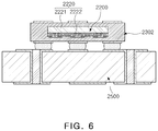
- FIG. 6 is a schematic cross-sectional view illustrating a case in which a fan-in semiconductor package is embedded in an interposer substrate and is ultimately mounted on a mainboard of an electronic device;
- FIG. 16 is a schematic plan view taken along the surface IV-IV′ of FIG. 15 ;
- FIG. 21 is a schematic cross-sectional view illustrating a semiconductor package according to an example embodiment.
- FIGS. 3A and 3B are schematic cross-sectional views illustrating states of a fan-in semiconductor package before and after being packaged.
- an exposure process may be performed on a unit package basis while moving a mask P on which a redistribution circuit pattern or a redistribution via pattern is drawn, but is not limited thereto, and a plurality of package units may be simultaneously exposed.
- (b) of FIG. 9 illustrates a process of forming a redistribution via 143 directly connected to the semiconductor chip.
- FIG. 9C a via hole penetrating through the insulating layer 141 is formed at an exposure point V of the mask P.
- FIG. 12 is a schematic plan view taken along surface III-III′ of FIG. 9 .
- connection structure 140 formed in a region of the mask P are aligned side by side, edges 140 - 1 , 140 - 2 , 140 - 3 , and 140 - 4 of the connection structure 140 of respective unit packages U 1 to U 8 do not penetrate within the width w of a cutting line. Therefore, individualized unit packages U 1 to U 8 may be obtained without a unit package cut by sawing.
- FIG. 15 is a schematic cross-sectional view illustrating a semiconductor package 100 A according to an example embodiment
- FIG. 16 is a schematic plan view taken along surface IV-IV′ of FIG. 15 .
- the electrical connection reliability between one side of the redistribution via 143 and the connection pad 122 by using the extension pad 124 as a medium may be secured, even when a mask matching process, for aligning an exposure point of a mask or a reticle on which a pattern of the redistribution via 143 is formed on the connection pad 122 of the semiconductor chip, is not performed.
- the other side of the redistribution via 143 may be in contact with a via pad 142 P formed in a portion of the redistribution layer 142 .
- the via pad 142 P is a connection portion of the redistribution via 143 and the redistribution layer 142 , and may have a width greater than a circuit width of the redistribution layer 142 .
- a horizontal cross-sectional area 142 Pa of the via pad 142 P may be equal to or smaller than a horizontal cross-sectional area 124 a of the extension pad 124 , and a shape of the redistribution via 143 may be a tapered shape having a smaller diameter toward one side of the redistribution via 143 .
- Matching of the extension pad 124 , the redistribution via 143 , and the redistribution layer 142 may be ensured without a mask matching process from the shapes of the via pad 142 P and the redistribution via 143 .
- the ratio ( 124 a / 122 a ) of the horizontal cross-sectional area 124 a of the extension pad 124 to the horizontal cross-sectional area 122 a of the connection pad 122 exceeds 6:1, a short between the extension pads 124 may occur, and when the ratio ( 124 a / 122 a ) thereof is less than 2:1, the exposure point of the mask or the reticle may not be located in the extension pad 124 in the photolithography process.
- the semiconductor package 100 A may further include a passivation film (or layer) 123 disposed on the first surface of the semiconductor chip 120 , in which at least a portion of the passivation film 123 is disposed between the connection pad 122 and the extension pad 124 , and having an opening exposing at least a portion of the connection pad 122 .
- the extension pad 124 may have a connection portion 124 - 2 filling an opening of the passivation film 123 and an extension portion 124 - 1 formed on the passivation film 123 and in contact with the redistribution via 143 .
- the horizontal cross-sectional area 124 a of the extension portion 124 - 1 of the extension pad may be greater than the horizontal cross-sectional area 124 b of the connection portion 124 - 2 , and the horizontal cross-sectional area 142 Pa of the via pad 142 P may be smaller than the horizontal cross-sectional area 124 a of the extension portion 124 - 1 of the extension pad.
- the semiconductor chip 120 may be an integrated circuit (IC) provided in an amount of several hundred to several million or more elements integrated in a single chip.
- the semiconductor chip 120 may be formed on the basis of an active wafer.
- a base material of the body 121 of the semiconductor chip 120 may be silicon (Si), germanium (Ge), gallium arsenide (GaAs), or the like.
- Various circuits may be formed on the body 121 .
- connection pads 122 may electrically connect the semiconductor chip 120 to other components.
- a material of each of the connection pads 122 may be a conductive material such as aluminum (Al), or the like without any particular limitation.
- a surface on which the connection pad 122 is disposed may be an active surface, and an opposite side thereof may be an inactive surface.
- the passivation film 123 covering at least a portion of the connection pad 122 may be formed on the body 121 as required.
- the passivation film 123 may be an oxide film, a nitride film, or the like, or may be a double layer of an oxide film and a nitride film.
- An insulating film (not shown), or the like may be further disposed at a necessary position.
- the semiconductor chip 120 may be a memory chip such as a volatile memory (for example, a dynamic random access memory (DRAM)), a non-volatile memory (for example, a read only memory (ROM)), a flash memory, or the like, an application processor chip such as a central processor (for example, a central processing unit (CPU)), a graphics processor (for example, a graphics processing unit (GPU)), a digital signal processor, a cryptographic processor, a microprocessor, a microcontroller, or the like, and a logic chip such as an analog-to-digital converter, an application-specific integrated circuit (ASIC), or the like.
- the semiconductor chip 120 is not limited thereto.
- a material of forming the extension pad 124 may be a conductive material such as cooper (Cu), aluminum (Al), and the like, without any particular limitation.
- the horizontal cross-sectional area 124 a of the extension pad 124 may be greater than the horizontal cross-sectional area 122 a of the connection pad 122 of the semiconductor chip, as described above.
- the ratio ( 124 a / 122 a ) of the horizontal cross-sectional area of the extension pad to the horizontal cross-sectional area 122 a of the connection pad may be 2:1 to 6:1, preferably 3:1 to 5:1, more preferably 4:1 to 5:1, and most preferably 5:1, as described above.
- the extension pad 124 may have the connection portion 124 - 2 filling an opening of the passivation film 123 and in contact with the connection pad 122 and an extension portion 124 - 1 formed on the passivation film 123 and in contact with the redistribution via 143 .
- the ratio ( 124 a / 124 b ) of the horizontal cross-sectional area 124 a of the extension portion 124 - 1 of the extension pad to the horizontal cross-sectional area 124 b of the connection portion 124 - 2 of the extension pad 124 may be 2:1 to 6:1, preferably 3:1 to 5:1, more preferably 4:1 to 5:1, and the most preferably 5:1, as described above.
- the encapsulant 130 may include an insulating material.
- a material including an inorganic filler and an insulating resin for example, a thermosetting resin such as an epoxy resin, a thermoplastic resin such as a polyimide resin, or a resin in which a reinforcing material such as an inorganic filler is included therein, specifically, Ajinomoto build-up film (ABF), Flame Resistant 4 (FR-4), and Bismaleimide Triazine (BT) may be used.
- ABS Ajinomoto build-up film
- FR-4 Flame Resistant 4
- BT Bismaleimide Triazine
- EMC epoxy molding compound
- PIE photo imageable encapsulant
- a material in which an insulating resin such as the thermosetting resin or the thermoplastic resin is impregnated in an inorganic filler and/or a core material such as a glass fiber, or the like, may be used as required.
- connection structure 140 may include the insulating layer 141 disposed on the active surface of the semiconductor chip 120 , the redistribution layer 142 disposed on the insulating layer 141 , and the redistribution via 143 connecting the redistribution layer 142 and the connection pad 122 of the semiconductor chip 120 .
- the connection structure 140 may include a more number of insulating layers, redistribution layers, and redistribution vias than illustrated in the drawings.
- the redistribution layer 142 is a portion connecting the redistribution via 143 and the underbump metal layer 160 , and may include the via pad 142 P.
- the via pad 142 P may have a width, greater than a circuit width of the redistribution layer 142 , and may be electrically connected to the redistribution via 143 .
- a horizontal cross-sectional area of the via pad 142 P may be smaller than the horizontal cross-sectional area 124 a of the extension pad 124 .
- At least one of the electrical connection metals 170 and/or at least one of the underbump metal layers 160 may be disposed in a fan-out region of the semiconductor chip 120 .
- the fan-out region may refer to a region except for a region in which the semiconductor chip 120 is disposed. That is, the semiconductor package 100 A according to the example embodiment may be a fan-out package.
- the fan-out package may have excellent reliability as compared to a fan-in package, may allow a plurality of I/O terminals to be implemented, and may facilitate a 3 D interconnection.
- the fan-out package may be manufactured to have a small thickness, and may have price competitiveness.
- a redistribution via 143 formed around the exposure point of the mask may not be located in a central portion of an extension pad 124 disposed on one surface of the semiconductor chip 120 . That is, at least a portion of a surface of the redistribution via 143 in contact with the extension pad 124 may be disposed to be outside of a region overlapping the connection pad 122 on a plane.
- a center axis 124 x of the extension pad 124 may be disposed to be shifted from a center axis 143 x of the redistribution via 143 .
- an interval between the center axis 120 x of the semiconductor chip and the center axis 140 x of the connection structure may be the same as an interval between the center axis 124 x of the extension pad and the center axis 143 x of the redistribution via.
- center axis 124 x of the extension pad 124 and the center axis 143 x of the redistribution via 143 may be interpreted as a center axis 124 x of each of at least portions of a plurality of extension pads 124 and a center axis 143 x of each of at least portions of a plurality of redistribution vias 143 , respectively.
- the extension pad 124 may have an extension portion 124 - 1 and a connection portion 124 - 2 , and at least a portion of the surface of the redistribution via 143 in contact with the extension portion 124 - 1 of the extension pad 124 may be disposed to be disposed to be outside of a region overlapping the connection portion 124 - 2 of the extension pad 124 on a plane.
- FIGS. 18 to 20 are schematic cross-sectional views illustrating semiconductor packages 100 C to 100 E according to example embodiments.
- a semiconductor chip 120 may be located in a horizontal cross-sectional region of a connection structure 140 .
- a first reference line C 1 parallel to a first edge of one side of the semiconductor chip 120 and a second reference line C 2 , parallel to a second edge of another side of the semiconductor chip 120 , orthogonal to each other at the center of the semiconductor chip 120 may have predetermined displacements, respectively, with respect to a third reference line C 3 , parallel to a third edge of one side of the connection structure 140 and a fourth reference line C 4 , parallel to a fourth edge of another side of the connection structure 140 , orthogonal to each other at the center of the connection structure 140 .
- the center of the semiconductor chip 120 is disposed to overlap with the center of the connection structure 140 , and the first reference line C 1 and/or the second reference line C 2 may form an acute angle with the third reference line C 3 and/or the fourth reference line C 4 , respectively, adjacent to each other.
- the center of the semiconductor chip 120 may be disposed to be offset from the center of the connection structure 140 , and the first reference line C 1 and/or the second reference line C 2 may form an acute angle with the third reference line C 3 and/or the fourth reference line C 4 , respectively, adjacent to each other.
- FIG. 21 is a schematic cross-sectional view illustrating a semiconductor package 100 F according to an example embodiment.
- the semiconductor package 100 F may further include a frame 110 having a through hole 110 H in which a semiconductor chip 120 is disposed.
- a center axis 124 x of an extension pad 124 may be disposed to be shifted from a center axis 143 x of a redistribution via 143
- a center axis 120 x of the semiconductor chip 120 may be disposed to be shifted from the center axis of the through hole 110 H and/or the center axis 140 x of a connection structure 140 .
- the frame 110 may further improve rigidity of the semiconductor package 100 depending on a specific material, and may serve to secure uniformity of thicknesses of an encapsulant 130 .
- the frame 110 may have at least one through hole 110 H.
- the through hole 110 H may penetrate through the frame 110 , and the semiconductor chip 120 may be disposed in the through hole 110 H.
- connection of a component to another component in the description includes an indirect connection through an adhesive layer as well as a direct connection between two components.
- electrically connected conceptually includes a physical connection and a physical disconnection. It can be understood that when an element is referred to with terms such as “first” and “second”, the element is not limited thereby. They may be used only for a purpose of distinguishing the element from the other elements, and may not limit the sequence or importance of the elements. In some cases, a first element may be referred to as a second element without departing from the scope of the claims set forth herein. Similarly, a second element may also be referred to as a first element.
Landscapes
- Physics & Mathematics (AREA)
- Geometry (AREA)
- Production Of Multi-Layered Print Wiring Board (AREA)
- Internal Circuitry In Semiconductor Integrated Circuit Devices (AREA)
Abstract
Description
Claims (19)
Applications Claiming Priority (2)
| Application Number | Priority Date | Filing Date | Title |
|---|---|---|---|
| KR10-2019-0045046 | 2019-04-17 | ||
| KR1020190045046A KR102821052B1 (en) | 2019-04-17 | 2019-04-17 | Semiconductor package |
Publications (2)
| Publication Number | Publication Date |
|---|---|
| US20200335468A1 US20200335468A1 (en) | 2020-10-22 |
| US11171107B2 true US11171107B2 (en) | 2021-11-09 |
Family
ID=72830884
Family Applications (1)
| Application Number | Title | Priority Date | Filing Date |
|---|---|---|---|
| US16/713,143 Active 2040-02-17 US11171107B2 (en) | 2019-04-17 | 2019-12-13 | Semiconductor package |
Country Status (3)
| Country | Link |
|---|---|
| US (1) | US11171107B2 (en) |
| KR (1) | KR102821052B1 (en) |
| CN (1) | CN111834319B (en) |
Citations (11)
| Publication number | Priority date | Publication date | Assignee | Title |
|---|---|---|---|---|
| KR100751663B1 (en) | 2006-09-06 | 2007-08-23 | 주식회사 하이닉스반도체 | Manufacturing Method of Semiconductor Device |
| US20160013148A1 (en) * | 2011-01-21 | 2016-01-14 | Stats Chippac, Ltd. | Semiconductor Device and Method of Forming Wafer-Level Interconnect Structures with Advanced Dielectric Characteristics |
| US20160338202A1 (en) * | 2015-05-11 | 2016-11-17 | Samsung Electro-Mechanics Co., Ltd. | Electronic component package and method of manufacturing the same |
| US9576919B2 (en) * | 2011-12-30 | 2017-02-21 | Deca Technologies Inc. | Semiconductor device and method comprising redistribution layers |
| US20170170127A1 (en) | 2015-12-11 | 2017-06-15 | SK Hynix Inc. | Semiconductors, packages, wafer level packages, and methods of manufacturing the same |
| KR20170070779A (en) | 2015-12-11 | 2017-06-22 | 에스케이하이닉스 주식회사 | Wafer level package and method for manufacturing the same |
| US9754835B2 (en) * | 2010-02-16 | 2017-09-05 | Deca Technologies Inc. | Semiconductor device and method comprising redistribution layers |
| US9899331B2 (en) * | 2016-03-31 | 2018-02-20 | Samsung Electro-Mechanics Co., Ltd. | Fan-out semiconductor package and method of manufacturing same |
| US10068853B2 (en) * | 2016-05-05 | 2018-09-04 | Taiwan Semiconductor Manufacturing Co., Ltd. | Integrated fan-out package and method of fabricating the same |
| US10128182B2 (en) * | 2016-09-14 | 2018-11-13 | Taiwan Semiconductor Manufacturing Company Ltd. | Semiconductor package structure and manufacturing method thereof |
| US10283473B1 (en) * | 2017-11-03 | 2019-05-07 | Taiwan Semiconductor Manufacturing Co., Ltd. | Package structure and manufacturing method thereof |
Family Cites Families (7)
| Publication number | Priority date | Publication date | Assignee | Title |
|---|---|---|---|---|
| US20070045845A1 (en) * | 2005-08-31 | 2007-03-01 | Anand Lal | Ball grid array interface structure and method |
| US8799845B2 (en) * | 2010-02-16 | 2014-08-05 | Deca Technologies Inc. | Adaptive patterning for panelized packaging |
| TWI474452B (en) * | 2011-09-22 | 2015-02-21 | 矽品精密工業股份有限公司 | Substrate, semiconductor package and method of manufacturing same |
| US9123600B2 (en) * | 2013-02-27 | 2015-09-01 | Invensas Corporation | Microelectronic package with consolidated chip structures |
| CN103730380B (en) * | 2013-12-05 | 2017-02-15 | 通富微电子股份有限公司 | Forming method of packaging structure |
| US9040316B1 (en) * | 2014-06-12 | 2015-05-26 | Deca Technologies Inc. | Semiconductor device and method of adaptive patterning for panelized packaging with dynamic via clipping |
| KR101963278B1 (en) * | 2016-10-28 | 2019-07-31 | 삼성전자주식회사 | Fan-out semiconductor package and manufacturing method for the same |
-
2019
- 2019-04-17 KR KR1020190045046A patent/KR102821052B1/en active Active
- 2019-12-13 US US16/713,143 patent/US11171107B2/en active Active
-
2020
- 2020-03-16 CN CN202010181672.2A patent/CN111834319B/en active Active
Patent Citations (12)
| Publication number | Priority date | Publication date | Assignee | Title |
|---|---|---|---|---|
| KR100751663B1 (en) | 2006-09-06 | 2007-08-23 | 주식회사 하이닉스반도체 | Manufacturing Method of Semiconductor Device |
| US20080057694A1 (en) | 2006-09-06 | 2008-03-06 | Hynix Semiconductor Inc. | Method for manufacturing semiconductor device |
| US9754835B2 (en) * | 2010-02-16 | 2017-09-05 | Deca Technologies Inc. | Semiconductor device and method comprising redistribution layers |
| US20160013148A1 (en) * | 2011-01-21 | 2016-01-14 | Stats Chippac, Ltd. | Semiconductor Device and Method of Forming Wafer-Level Interconnect Structures with Advanced Dielectric Characteristics |
| US9576919B2 (en) * | 2011-12-30 | 2017-02-21 | Deca Technologies Inc. | Semiconductor device and method comprising redistribution layers |
| US20160338202A1 (en) * | 2015-05-11 | 2016-11-17 | Samsung Electro-Mechanics Co., Ltd. | Electronic component package and method of manufacturing the same |
| US20170170127A1 (en) | 2015-12-11 | 2017-06-15 | SK Hynix Inc. | Semiconductors, packages, wafer level packages, and methods of manufacturing the same |
| KR20170070779A (en) | 2015-12-11 | 2017-06-22 | 에스케이하이닉스 주식회사 | Wafer level package and method for manufacturing the same |
| US9899331B2 (en) * | 2016-03-31 | 2018-02-20 | Samsung Electro-Mechanics Co., Ltd. | Fan-out semiconductor package and method of manufacturing same |
| US10068853B2 (en) * | 2016-05-05 | 2018-09-04 | Taiwan Semiconductor Manufacturing Co., Ltd. | Integrated fan-out package and method of fabricating the same |
| US10128182B2 (en) * | 2016-09-14 | 2018-11-13 | Taiwan Semiconductor Manufacturing Company Ltd. | Semiconductor package structure and manufacturing method thereof |
| US10283473B1 (en) * | 2017-11-03 | 2019-05-07 | Taiwan Semiconductor Manufacturing Co., Ltd. | Package structure and manufacturing method thereof |
Also Published As
| Publication number | Publication date |
|---|---|
| CN111834319A (en) | 2020-10-27 |
| US20200335468A1 (en) | 2020-10-22 |
| KR102821052B1 (en) | 2025-06-16 |
| CN111834319B (en) | 2024-07-16 |
| KR20200122153A (en) | 2020-10-27 |
Similar Documents
| Publication | Publication Date | Title |
|---|---|---|
| US11195790B2 (en) | Fan-out semiconductor package | |
| US10607914B2 (en) | Semiconductor package | |
| US10217631B2 (en) | Fan-out semiconductor package | |
| US10504825B2 (en) | Fan-out semiconductor package | |
| US10177100B2 (en) | Fan-out semiconductor package | |
| US10438927B2 (en) | Fan-out semiconductor package | |
| US20190131253A1 (en) | Fan-out semiconductor package | |
| US10741461B2 (en) | Fan-out semiconductor package | |
| US10304807B2 (en) | Fan-out semiconductor package | |
| US11557534B2 (en) | Semiconductor package | |
| US10410961B2 (en) | Fan-out semiconductor package | |
| US9935068B2 (en) | Fan-out semiconductor package | |
| US10312195B2 (en) | Fan-out semiconductor package | |
| US20190139920A1 (en) | Fan-out semiconductor package | |
| US11069666B2 (en) | Semiconductor package | |
| US10622322B2 (en) | Fan-out semiconductor package and method of manufacturing the fan-out semiconductor | |
| US20210375805A1 (en) | Semiconductor package substrate and method of manufacturing semiconductor package using the same | |
| US10515916B2 (en) | Fan-out semiconductor package | |
| US10770403B2 (en) | Fan-out semiconductor package | |
| US11652066B2 (en) | Semiconductor package | |
| US11171107B2 (en) | Semiconductor package | |
| US20190164894A1 (en) | Fan-out semiconductor package |
Legal Events
| Date | Code | Title | Description |
|---|---|---|---|
| AS | Assignment |
Owner name: SAMSUNG ELECTRONICS CO., LTD., KOREA, REPUBLIC OF Free format text: ASSIGNMENT OF ASSIGNORS INTEREST;ASSIGNORS:CHOI, GYU JIN;KIM, SUNG HOAN;JOO, CHANG EUN;AND OTHERS;REEL/FRAME:051273/0354 Effective date: 20190924 |
|
| FEPP | Fee payment procedure |
Free format text: ENTITY STATUS SET TO UNDISCOUNTED (ORIGINAL EVENT CODE: BIG.); ENTITY STATUS OF PATENT OWNER: LARGE ENTITY |
|
| STPP | Information on status: patent application and granting procedure in general |
Free format text: DOCKETED NEW CASE - READY FOR EXAMINATION |
|
| STPP | Information on status: patent application and granting procedure in general |
Free format text: NON FINAL ACTION MAILED |
|
| STPP | Information on status: patent application and granting procedure in general |
Free format text: RESPONSE TO NON-FINAL OFFICE ACTION ENTERED AND FORWARDED TO EXAMINER |
|
| STPP | Information on status: patent application and granting procedure in general |
Free format text: NOTICE OF ALLOWANCE MAILED -- APPLICATION RECEIVED IN OFFICE OF PUBLICATIONS |
|
| STPP | Information on status: patent application and granting procedure in general |
Free format text: PUBLICATIONS -- ISSUE FEE PAYMENT VERIFIED |
|
| STCF | Information on status: patent grant |
Free format text: PATENTED CASE |
|
| MAFP | Maintenance fee payment |
Free format text: PAYMENT OF MAINTENANCE FEE, 4TH YEAR, LARGE ENTITY (ORIGINAL EVENT CODE: M1551); ENTITY STATUS OF PATENT OWNER: LARGE ENTITY Year of fee payment: 4 |