US11139299B2 - FinFET based ZRAM with convex channel region - Google Patents
FinFET based ZRAM with convex channel region Download PDFInfo
- Publication number
- US11139299B2 US11139299B2 US16/444,386 US201916444386A US11139299B2 US 11139299 B2 US11139299 B2 US 11139299B2 US 201916444386 A US201916444386 A US 201916444386A US 11139299 B2 US11139299 B2 US 11139299B2
- Authority
- US
- United States
- Prior art keywords
- channel portion
- convex
- finned
- gate
- channel region
- Prior art date
- Legal status (The legal status is an assumption and is not a legal conclusion. Google has not performed a legal analysis and makes no representation as to the accuracy of the status listed.)
- Active
Links
- 125000006850 spacer group Chemical group 0.000 claims abstract description 44
- 238000000034 method Methods 0.000 claims abstract description 41
- 239000004065 semiconductor Substances 0.000 claims abstract description 36
- 229910052751 metal Inorganic materials 0.000 claims abstract description 24
- 239000002184 metal Substances 0.000 claims abstract description 24
- 239000000463 material Substances 0.000 claims abstract description 8
- 239000010410 layer Substances 0.000 claims description 18
- 239000000758 substrate Substances 0.000 claims description 15
- 239000011229 interlayer Substances 0.000 claims description 10
- 229910052710 silicon Inorganic materials 0.000 claims description 8
- 239000010703 silicon Substances 0.000 claims description 8
- 229910052732 germanium Inorganic materials 0.000 claims description 5
- GNPVGFCGXDBREM-UHFFFAOYSA-N germanium atom Chemical compound [Ge] GNPVGFCGXDBREM-UHFFFAOYSA-N 0.000 claims description 5
- 229910052738 indium Inorganic materials 0.000 claims description 3
- APFVFJFRJDLVQX-UHFFFAOYSA-N indium atom Chemical compound [In] APFVFJFRJDLVQX-UHFFFAOYSA-N 0.000 claims description 3
- GYHNNYVSQQEPJS-UHFFFAOYSA-N Gallium Chemical compound [Ga] GYHNNYVSQQEPJS-UHFFFAOYSA-N 0.000 claims 1
- 229910052733 gallium Inorganic materials 0.000 claims 1
- 238000004519 manufacturing process Methods 0.000 abstract description 14
- 230000005669 field effect Effects 0.000 abstract description 2
- 230000008569 process Effects 0.000 description 14
- 239000012212 insulator Substances 0.000 description 7
- XUIMIQQOPSSXEZ-UHFFFAOYSA-N Silicon Chemical compound [Si] XUIMIQQOPSSXEZ-UHFFFAOYSA-N 0.000 description 6
- 210000004027 cell Anatomy 0.000 description 5
- 238000009413 insulation Methods 0.000 description 5
- VYPSYNLAJGMNEJ-UHFFFAOYSA-N Silicium dioxide Chemical compound O=[Si]=O VYPSYNLAJGMNEJ-UHFFFAOYSA-N 0.000 description 4
- GWEVSGVZZGPLCZ-UHFFFAOYSA-N Titan oxide Chemical compound O=[Ti]=O GWEVSGVZZGPLCZ-UHFFFAOYSA-N 0.000 description 4
- 230000006870 function Effects 0.000 description 4
- 230000003647 oxidation Effects 0.000 description 4
- 238000007254 oxidation reaction Methods 0.000 description 4
- 229910052814 silicon oxide Inorganic materials 0.000 description 4
- 239000011800 void material Substances 0.000 description 4
- 229910000577 Silicon-germanium Inorganic materials 0.000 description 3
- LEVVHYCKPQWKOP-UHFFFAOYSA-N [Si].[Ge] Chemical compound [Si].[Ge] LEVVHYCKPQWKOP-UHFFFAOYSA-N 0.000 description 3
- 239000003990 capacitor Substances 0.000 description 3
- 230000000694 effects Effects 0.000 description 3
- 229910000449 hafnium oxide Inorganic materials 0.000 description 3
- WIHZLLGSGQNAGK-UHFFFAOYSA-N hafnium(4+);oxygen(2-) Chemical compound [O-2].[O-2].[Hf+4] WIHZLLGSGQNAGK-UHFFFAOYSA-N 0.000 description 3
- 238000002955 isolation Methods 0.000 description 3
- RVTZCBVAJQQJTK-UHFFFAOYSA-N oxygen(2-);zirconium(4+) Chemical compound [O-2].[O-2].[Zr+4] RVTZCBVAJQQJTK-UHFFFAOYSA-N 0.000 description 3
- 229910001928 zirconium oxide Inorganic materials 0.000 description 3
- 229910000530 Gallium indium arsenide Inorganic materials 0.000 description 2
- GPXJNWSHGFTCBW-UHFFFAOYSA-N Indium phosphide Chemical compound [In]#P GPXJNWSHGFTCBW-UHFFFAOYSA-N 0.000 description 2
- KXNLCSXBJCPWGL-UHFFFAOYSA-N [Ga].[As].[In] Chemical compound [Ga].[As].[In] KXNLCSXBJCPWGL-UHFFFAOYSA-N 0.000 description 2
- 150000002739 metals Chemical class 0.000 description 2
- OGIDPMRJRNCKJF-UHFFFAOYSA-N titanium oxide Inorganic materials [Ti]=O OGIDPMRJRNCKJF-UHFFFAOYSA-N 0.000 description 2
- 230000004075 alteration Effects 0.000 description 1
- 230000000712 assembly Effects 0.000 description 1
- 238000000429 assembly Methods 0.000 description 1
- 230000008021 deposition Effects 0.000 description 1
- RPQDHPTXJYYUPQ-UHFFFAOYSA-N indium arsenide Chemical compound [In]#[As] RPQDHPTXJYYUPQ-UHFFFAOYSA-N 0.000 description 1
- 238000012986 modification Methods 0.000 description 1
- 230000004048 modification Effects 0.000 description 1
- 208000001491 myopia Diseases 0.000 description 1
- 229910021420 polycrystalline silicon Inorganic materials 0.000 description 1
- 229920005591 polysilicon Polymers 0.000 description 1
- 210000000352 storage cell Anatomy 0.000 description 1
- 239000004408 titanium dioxide Substances 0.000 description 1
Images


Classifications
-
- H01L27/10802—
-
- H01L27/10844—
-
- H—ELECTRICITY
- H01—ELECTRIC ELEMENTS
- H01L—SEMICONDUCTOR DEVICES NOT COVERED BY CLASS H10
- H01L29/00—Semiconductor devices adapted for rectifying, amplifying, oscillating or switching, or capacitors or resistors with at least one potential-jump barrier or surface barrier, e.g. PN junction depletion layer or carrier concentration layer; Details of semiconductor bodies or of electrodes thereof ; Multistep manufacturing processes therefor
- H01L29/02—Semiconductor bodies ; Multistep manufacturing processes therefor
- H01L29/06—Semiconductor bodies ; Multistep manufacturing processes therefor characterised by their shape; characterised by the shapes, relative sizes, or dispositions of the semiconductor regions ; characterised by the concentration or distribution of impurities within semiconductor regions
- H01L29/10—Semiconductor bodies ; Multistep manufacturing processes therefor characterised by their shape; characterised by the shapes, relative sizes, or dispositions of the semiconductor regions ; characterised by the concentration or distribution of impurities within semiconductor regions with semiconductor regions connected to an electrode not carrying current to be rectified, amplified or switched and such electrode being part of a semiconductor device which comprises three or more electrodes
- H01L29/1025—Channel region of field-effect devices
- H01L29/1029—Channel region of field-effect devices of field-effect transistors
- H01L29/1033—Channel region of field-effect devices of field-effect transistors with insulated gate, e.g. characterised by the length, the width, the geometric contour or the doping structure
- H01L29/1054—Channel region of field-effect devices of field-effect transistors with insulated gate, e.g. characterised by the length, the width, the geometric contour or the doping structure with a variation of the composition, e.g. channel with strained layer for increasing the mobility
-
- H—ELECTRICITY
- H01—ELECTRIC ELEMENTS
- H01L—SEMICONDUCTOR DEVICES NOT COVERED BY CLASS H10
- H01L29/00—Semiconductor devices adapted for rectifying, amplifying, oscillating or switching, or capacitors or resistors with at least one potential-jump barrier or surface barrier, e.g. PN junction depletion layer or carrier concentration layer; Details of semiconductor bodies or of electrodes thereof ; Multistep manufacturing processes therefor
- H01L29/66—Types of semiconductor device ; Multistep manufacturing processes therefor
- H01L29/66007—Multistep manufacturing processes
- H01L29/66075—Multistep manufacturing processes of devices having semiconductor bodies comprising group 14 or group 13/15 materials
- H01L29/66227—Multistep manufacturing processes of devices having semiconductor bodies comprising group 14 or group 13/15 materials the devices being controllable only by the electric current supplied or the electric potential applied, to an electrode which does not carry the current to be rectified, amplified or switched, e.g. three-terminal devices
- H01L29/66409—Unipolar field-effect transistors
- H01L29/66477—Unipolar field-effect transistors with an insulated gate, i.e. MISFET
- H01L29/6653—Unipolar field-effect transistors with an insulated gate, i.e. MISFET using the removal of at least part of spacer, e.g. disposable spacer
-
- H—ELECTRICITY
- H01—ELECTRIC ELEMENTS
- H01L—SEMICONDUCTOR DEVICES NOT COVERED BY CLASS H10
- H01L29/00—Semiconductor devices adapted for rectifying, amplifying, oscillating or switching, or capacitors or resistors with at least one potential-jump barrier or surface barrier, e.g. PN junction depletion layer or carrier concentration layer; Details of semiconductor bodies or of electrodes thereof ; Multistep manufacturing processes therefor
- H01L29/66—Types of semiconductor device ; Multistep manufacturing processes therefor
- H01L29/66007—Multistep manufacturing processes
- H01L29/66075—Multistep manufacturing processes of devices having semiconductor bodies comprising group 14 or group 13/15 materials
- H01L29/66227—Multistep manufacturing processes of devices having semiconductor bodies comprising group 14 or group 13/15 materials the devices being controllable only by the electric current supplied or the electric potential applied, to an electrode which does not carry the current to be rectified, amplified or switched, e.g. three-terminal devices
- H01L29/66409—Unipolar field-effect transistors
- H01L29/66477—Unipolar field-effect transistors with an insulated gate, i.e. MISFET
- H01L29/66545—Unipolar field-effect transistors with an insulated gate, i.e. MISFET using a dummy, i.e. replacement gate in a process wherein at least a part of the final gate is self aligned to the dummy gate
-
- H—ELECTRICITY
- H01—ELECTRIC ELEMENTS
- H01L—SEMICONDUCTOR DEVICES NOT COVERED BY CLASS H10
- H01L29/00—Semiconductor devices adapted for rectifying, amplifying, oscillating or switching, or capacitors or resistors with at least one potential-jump barrier or surface barrier, e.g. PN junction depletion layer or carrier concentration layer; Details of semiconductor bodies or of electrodes thereof ; Multistep manufacturing processes therefor
- H01L29/66—Types of semiconductor device ; Multistep manufacturing processes therefor
- H01L29/66007—Multistep manufacturing processes
- H01L29/66075—Multistep manufacturing processes of devices having semiconductor bodies comprising group 14 or group 13/15 materials
- H01L29/66227—Multistep manufacturing processes of devices having semiconductor bodies comprising group 14 or group 13/15 materials the devices being controllable only by the electric current supplied or the electric potential applied, to an electrode which does not carry the current to be rectified, amplified or switched, e.g. three-terminal devices
- H01L29/66409—Unipolar field-effect transistors
- H01L29/66477—Unipolar field-effect transistors with an insulated gate, i.e. MISFET
- H01L29/6656—Unipolar field-effect transistors with an insulated gate, i.e. MISFET using multiple spacer layers, e.g. multiple sidewall spacers
-
- H—ELECTRICITY
- H01—ELECTRIC ELEMENTS
- H01L—SEMICONDUCTOR DEVICES NOT COVERED BY CLASS H10
- H01L29/00—Semiconductor devices adapted for rectifying, amplifying, oscillating or switching, or capacitors or resistors with at least one potential-jump barrier or surface barrier, e.g. PN junction depletion layer or carrier concentration layer; Details of semiconductor bodies or of electrodes thereof ; Multistep manufacturing processes therefor
- H01L29/66—Types of semiconductor device ; Multistep manufacturing processes therefor
- H01L29/66007—Multistep manufacturing processes
- H01L29/66075—Multistep manufacturing processes of devices having semiconductor bodies comprising group 14 or group 13/15 materials
- H01L29/66227—Multistep manufacturing processes of devices having semiconductor bodies comprising group 14 or group 13/15 materials the devices being controllable only by the electric current supplied or the electric potential applied, to an electrode which does not carry the current to be rectified, amplified or switched, e.g. three-terminal devices
- H01L29/66409—Unipolar field-effect transistors
- H01L29/66477—Unipolar field-effect transistors with an insulated gate, i.e. MISFET
- H01L29/66787—Unipolar field-effect transistors with an insulated gate, i.e. MISFET with a gate at the side of the channel
- H01L29/66795—Unipolar field-effect transistors with an insulated gate, i.e. MISFET with a gate at the side of the channel with a horizontal current flow in a vertical sidewall of a semiconductor body, e.g. FinFET, MuGFET
-
- H—ELECTRICITY
- H01—ELECTRIC ELEMENTS
- H01L—SEMICONDUCTOR DEVICES NOT COVERED BY CLASS H10
- H01L29/00—Semiconductor devices adapted for rectifying, amplifying, oscillating or switching, or capacitors or resistors with at least one potential-jump barrier or surface barrier, e.g. PN junction depletion layer or carrier concentration layer; Details of semiconductor bodies or of electrodes thereof ; Multistep manufacturing processes therefor
- H01L29/66—Types of semiconductor device ; Multistep manufacturing processes therefor
- H01L29/68—Types of semiconductor device ; Multistep manufacturing processes therefor controllable by only the electric current supplied, or only the electric potential applied, to an electrode which does not carry the current to be rectified, amplified or switched
- H01L29/76—Unipolar devices, e.g. field effect transistors
- H01L29/772—Field effect transistors
- H01L29/78—Field effect transistors with field effect produced by an insulated gate
- H01L29/7841—Field effect transistors with field effect produced by an insulated gate with floating body, e.g. programmable transistors
-
- H—ELECTRICITY
- H01—ELECTRIC ELEMENTS
- H01L—SEMICONDUCTOR DEVICES NOT COVERED BY CLASS H10
- H01L29/00—Semiconductor devices adapted for rectifying, amplifying, oscillating or switching, or capacitors or resistors with at least one potential-jump barrier or surface barrier, e.g. PN junction depletion layer or carrier concentration layer; Details of semiconductor bodies or of electrodes thereof ; Multistep manufacturing processes therefor
- H01L29/66—Types of semiconductor device ; Multistep manufacturing processes therefor
- H01L29/68—Types of semiconductor device ; Multistep manufacturing processes therefor controllable by only the electric current supplied, or only the electric potential applied, to an electrode which does not carry the current to be rectified, amplified or switched
- H01L29/76—Unipolar devices, e.g. field effect transistors
- H01L29/772—Field effect transistors
- H01L29/78—Field effect transistors with field effect produced by an insulated gate
- H01L29/785—Field effect transistors with field effect produced by an insulated gate having a channel with a horizontal current flow in a vertical sidewall of a semiconductor body, e.g. FinFET, MuGFET
-
- H—ELECTRICITY
- H10—SEMICONDUCTOR DEVICES; ELECTRIC SOLID-STATE DEVICES NOT OTHERWISE PROVIDED FOR
- H10B—ELECTRONIC MEMORY DEVICES
- H10B12/00—Dynamic random access memory [DRAM] devices
- H10B12/01—Manufacture or treatment
-
- H—ELECTRICITY
- H10—SEMICONDUCTOR DEVICES; ELECTRIC SOLID-STATE DEVICES NOT OTHERWISE PROVIDED FOR
- H10B—ELECTRONIC MEMORY DEVICES
- H10B12/00—Dynamic random access memory [DRAM] devices
- H10B12/20—DRAM devices comprising floating-body transistors, e.g. floating-body cells
-
- H—ELECTRICITY
- H01—ELECTRIC ELEMENTS
- H01L—SEMICONDUCTOR DEVICES NOT COVERED BY CLASS H10
- H01L29/00—Semiconductor devices adapted for rectifying, amplifying, oscillating or switching, or capacitors or resistors with at least one potential-jump barrier or surface barrier, e.g. PN junction depletion layer or carrier concentration layer; Details of semiconductor bodies or of electrodes thereof ; Multistep manufacturing processes therefor
- H01L29/02—Semiconductor bodies ; Multistep manufacturing processes therefor
- H01L29/12—Semiconductor bodies ; Multistep manufacturing processes therefor characterised by the materials of which they are formed
- H01L29/122—Single quantum well structures
-
- H—ELECTRICITY
- H01—ELECTRIC ELEMENTS
- H01L—SEMICONDUCTOR DEVICES NOT COVERED BY CLASS H10
- H01L29/00—Semiconductor devices adapted for rectifying, amplifying, oscillating or switching, or capacitors or resistors with at least one potential-jump barrier or surface barrier, e.g. PN junction depletion layer or carrier concentration layer; Details of semiconductor bodies or of electrodes thereof ; Multistep manufacturing processes therefor
- H01L29/02—Semiconductor bodies ; Multistep manufacturing processes therefor
- H01L29/12—Semiconductor bodies ; Multistep manufacturing processes therefor characterised by the materials of which they are formed
- H01L29/16—Semiconductor bodies ; Multistep manufacturing processes therefor characterised by the materials of which they are formed including, apart from doping materials or other impurities, only elements of Group IV of the Periodic System
- H01L29/161—Semiconductor bodies ; Multistep manufacturing processes therefor characterised by the materials of which they are formed including, apart from doping materials or other impurities, only elements of Group IV of the Periodic System including two or more of the elements provided for in group H01L29/16, e.g. alloys
- H01L29/165—Semiconductor bodies ; Multistep manufacturing processes therefor characterised by the materials of which they are formed including, apart from doping materials or other impurities, only elements of Group IV of the Periodic System including two or more of the elements provided for in group H01L29/16, e.g. alloys in different semiconductor regions, e.g. heterojunctions
Definitions
- the present invention relates generally to semiconductor fabrication, and more particularly, to fabrication of ZRAM devices.
- Dynamic random access memory is utilized in many electronic devices. These include computers, mobile devices, tablets, and consumer electronics, to name a few. A continuous goal is increasing of the circuit density, thus increasing the amount of memory in a physical package. This enables increasingly powerful computing power in smaller, more portable devices.
- Zero capacitance random access memory is a type of DRAM memory based on the floating body effect. In ZRAM, the floating body effect allows the memory cell to be built without adding a separate capacitor, as the floating body effect takes the place of the conventional capacitor.
- ZRAM Zero capacitance random access memory
- embodiments of the present invention provide a semiconductor structure, comprising: a semiconductor substrate; a semiconductor fin disposed on the semiconductor substrate; a channel region comprising: a finned channel portion; and a convex channel portion disposed around the finned channel portion, wherein the channel region comprises an elongated surface and a short surface; a metal gate disposed around the elongated surface of the channel region; a first spacer disposed adjacent to the metal gate and in direct physical contact with the short surface of the channel region; and a second spacer disposed adjacent to the first spacer.
- embodiments of the present invention provide a semiconductor structure, comprising: a semiconductor substrate; a semiconductor fin disposed on the semiconductor substrate; a channel region comprising: a finned channel portion; and a convex channel portion disposed around the finned channel portion, wherein the channel region comprises an elongated surface and a short surface; a metal gate disposed around the elongated surface of the channel region and the short surface of the channel region; and a spacer disposed adjacent to the metal gate.
- embodiments of the present invention provide a method of forming a semiconductor structure, comprising: forming a semiconductor fin on a semiconductor substrate; forming a sacrificial gate structure; forming a first spacer adjacent to the sacrificial gate structure; forming a second spacer adjacent to the first spacer; forming source/drain regions adjacent to the second spacer; removing the sacrificial gate structure; forming a convex channel region; and forming a metal gate structure.
- FIGs. The figures are intended to be illustrative, not limiting.
- cross-sectional views may be in the form of “slices”, or “near-sighted” cross-sectional views, omitting certain background lines which would otherwise be visible in a “true” cross-sectional view, for illustrative clarity.
- FIG. 1A shows a perspective view of an embodiment of the present invention.
- FIG. 1B shows a perspective view of an alternative embodiment of the present invention.
- FIG. 2 shows an X-Y cross section of an embodiment of the present invention.
- FIG. 3 shows a Y-Z cross section of an embodiment of the present invention.
- FIG. 4 shows an X-Z cross section of an embodiment of the present invention.
- FIG. 5 shows an X-Y cross section of an alternative embodiment of the present invention.
- FIG. 6 shows an X-Z cross section of an alternative embodiment of the present invention.
- FIG. 7 shows an X-Y cross section of an embodiment at an intermediate fabrication step with dummy gates.
- FIG. 8A shows an X-Y cross section of an embodiment after a subsequent fabrication step of dummy gate removal.
- FIG. 8B shows an X-Y cross section of an embodiment after a subsequent fabrication step of forming the convex channel region.
- FIG. 9 shows an X-Y cross section of an embodiment after a subsequent fabrication step of first spacer removal.
- FIG. 10 is a flowchart indicating process steps for embodiments of the present invention.
- Embodiments of the present invention provide improved methods and structures for fabrication of capacitor-less DRAM devices. Such devices, sometimes referred to as ZRAM devices, implement a dynamic random access memory without the use of a capacitor in each storage cell.
- a channel is formed in a fin-type field effect transistor (finFET) that is comprised of a finned channel portion and a convex channel portion.
- the finned channel portion may be comprised of a first semiconductor material and the convex channel portion may be comprised of a second, different semiconductor material.
- a metal gate is disposed around the elongated surface of the channel region, but is not disposed on the short surface of the channel region.
- a first spacer is disposed adjacent to the gate and in direct physical contact with the short surface of the channel region, and a second spacer is disposed adjacent to the first spacer.
- FIG. 1A shows a perspective view of a semiconductor structure 100 in accordance with an embodiment of the present invention.
- Semiconductor structure 100 comprises semiconductor substrate 102 .
- Substrate 102 may comprise a bulk substrate such as a silicon wafer.
- a local trench isolation (LTI) insulator layer 106 is disposed on the substrate 102 .
- a semiconductor fin 104 extends from the substrate 102 .
- a metal gate 108 is formed over the fin 104 .
- Spacers 110 are formed on each side of gate 108 . While only one set of spacers is shown in this drawing, other embodiments may have additional spacers, as is shown in other drawings.
- FIG. 1B shows a perspective view of a semiconductor structure 101 in accordance with an alternative embodiment of the present invention.
- Semiconductor structure 101 is similar to semiconductor structure 100 of FIG. 1B , except that semiconductor structure 101 comprises local trench isolation (LTI) insulator layer 107 that is disposed on the substrate 102 , and serves to electrically isolate fin 104 from substrate 102 , whereas fin 104 of semiconductor structure 100 in FIG. 1A protrudes through insulator layer 106 .
- the electrical isolation of fin 104 starts with a structure such as shown in FIG. 1A .
- a fin oxidation (FOX) process oxidizes a lower portion of fin 104 , effectively converting it to oxide (e.g. silicon oxide).
- oxide e.g. silicon oxide
- the FOX process includes a thermal oxidation process.
- embodiments of the present invention may also utilize a conventional semiconductor-on-insulator structure.
- FIG. 1A and FIG. 1B are intended to provide reference in the X, Y, and Z planes for the figures that follow. Legend 117 indicates the X axis, Y axis, and Z axis for these figures. Various details of the convex channel are not visible in FIG. 1A or FIG. 1B , as it is covered by the gate and spacers. Subsequent figures show various “slices” and cross sections to illustrate features of the various embodiments.
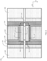
- FIG. 2 shows an X-Y cross section of a structure 200 in accordance with an embodiment of the present invention, as viewed along line A-A′ of FIG. 1B .
- Structure 200 includes a channel region 231 which includes finned channel portion 236 and a convex channel portion 234 .
- the channel region 231 comprises an elongated surface 237 and a short surface 239 .
- the convex channel portion 234 is disposed around the finned channel portion 236 .
- a gate 224 is formed around the elongated surface 237 of the channel region 231 .
- Disposed between the gate 224 and channel region 231 is a gate dielectric layer 230 .
- an oxide interlayer 232 may be disposed between the gate dielectric layer 230 and the channel region 231 .
- the channel region 231 is a so-called convex channel because it is wider than the fin.
- the convex channel portion 234 is comprised of silicon germanium (SiGe), and the finned channel portion 236 is comprised of silicon (which does not include germanium).
- the germanium concentration of the SiGe that comprises the convex channel portion 234 ranges from about 20 percent to about 40 percent, by atomic weight.
- the convex channel portion 234 comprises indium phosphide (InP), and the finned channel portion 236 is comprised of silicon or silicon germanium.
- the convex channel portion 234 comprises silicon (which does not include germanium), and the finned channel portion 236 comprises indium.
- the finned channel portion 236 may include, but is not limited to, indium phosphide (InP), indium arsenide (InAs), and/or indium gallium arsenide (InGaAs).
- the convex channel portion 234 comprises silicon and also includes germanium (SiGe).
- a first spacer 228 is disposed adjacent to the gate 224 and in direct physical contact with the short surface 239 of the channel region 231 .
- the gate 224 is disposed only along the elongated side of the channel region 231 , and the gate does not cover the short surface 239 of the channel region 231 .
- the first spacer 228 may include, but is not limited to, hafnium oxide, titanium oxide, and/or zirconium oxide.
- the first spacer 228 is preferably a High-K (K>4) material.
- a second spacer is disposed adjacent to the first spacer.
- the second spacer is comprised of silicon oxide.
- the source/drain regions 220 may comprise an epitaxially grown semiconductor material such as epitaxial silicon or epitaxial silicon germanium. Doped extension regions 238 may extend into the channel region 231 .
- FIG. 3 shows a Y-Z cross section of a semiconductor structure 300 in accordance with an embodiment of the present invention, as viewed along line B-B′ of FIG. 1B .
- similar elements may be referred to by similar numbers in various figures (FIGs) of the drawing, in which case typically the last two significant digits may be the same.
- gate 324 of FIG. 3 is similar to gate 224 of FIG. 2 .
- the finned channel portion 336 is isolated from substrate 302 by insulation layer 307 , which may be formed by a fin oxidation (FOX) process.
- the convex channel portion 334 is disposed around the finned channel portion 336 .
- An oxide interlayer 332 is disposed around the convex channel portion 334 .
- a gate dielectric layer 330 is disposed around the oxide interlayer 332 .
- the gate dielectric layer 330 is comprised of hafnium oxide, titanium dioxide, and/or zirconium oxide.
- Gate 324 is disposed on gate dielectric layer 330 .
- FIG. 4 shows an X-Z cross section of a semiconductor structure 400 in accordance with an embodiment of the present invention, as viewed along line C-C′ of FIG. 1B .
- insulation layer 407 is localized, and disposed under finned channel portion 436 .
- SOI semiconductor-on-insulator
- FIG. 5 shows an X-Y cross section of a semiconductor structure 500 in accordance with an alternative embodiment of the present invention. Please refer to line A-A′ of FIG. 1B for an orientation reference.
- there is only one spacer 526 which is the outer spacer (compare with 226 of FIG. 2 ).
- the first spacer ( 228 of FIG. 2 ) is not present in this embodiment.
- the gate 524 , gate dielectric 530 and oxide interlayer 532 surround the channel region 531 on both the elongated surface 537 and the short surface 539 .
- the channel region 531 includes a convex channel portion 534 .
- FIG. 6 shows an X-Z cross section of a semiconductor structure 600 in accordance with an alternative embodiment of the present invention. Please refer to line C-C′ of FIG. 1B for an orientation reference.
- insulation layer 607 is localized, and disposed under finned channel portion 636 .
- SOI semiconductor-on-insulator
- spacer 626 is not in direct physical contact with convex channel portion 634 .
- the gate 624 , gate dielectric 630 , and oxide interlayer 632 envelope the convex channel portion 634 .
- FIG. 7 shows an X-Y cross section of structure 700 in accordance with an embodiment at an intermediate fabrication step with dummy gate 725 .
- a dummy gate oxide 735 may also be deposited prior to deposition of dummy (sacrificial) gate 725 .
- dummy gate 725 is comprised of polysilicon.
- dummy gate oxide 735 is comprised of silicon oxide.
- FIG. 8A shows an X-Y cross section of structure 800 in accordance with an embodiment at a subsequent fabrication step of dummy gate removal.
- the dummy gate and dummy gate oxide are removed, forming void 841 .
- FIG. 8B shows structure 800 after a subsequent process step of forming the convex channel 834 .
- a new metal gate stack which may include gate dielectric layers, work function metals (not shown), and one or more fill metals is formed in void 841 , and is thus, self-aligned to the spacers 828 .
- Spacers 828 and spacers 826 are comprised of different materials to facilitate selective removal, if desired.
- spacers 828 are comprised of a high-K dielectric layer such as hafnium oxide, titanium oxide, and/or zirconium oxide, while spacers 826 are comprised of silicon oxide.
- RMG replacement metal gate
- structure 800 is then converted to a structure as depicted in structure 200 of FIG. 2 .
- a wrap-around replacement metal gate process may be used, as is further explained and shown in FIG. 9 .
- FIG. 9 shows an X-Y cross section of structure 900 in accordance with an embodiment at a subsequent fabrication step of first spacer removal.
- the first spacers ( 828 in FIG. 8 ) are selectively removed.
- a wet etch process is used to remove the first spacers.
- void 941 is expanded as compared with void 841 in FIG. 8 .
- a replacement metal gate process may be used, resulting in the wrap-around metal gate 524 (see FIG. 5 ) which envelopes both the elongated surface 537 and the short surface 539 .
- Methods in accordance with illustrative embodiments provide the wrap-around gate in a self-aligned process, improving the ease of manufacturing and improving yield.
- FIG. 10 is a flowchart 1000 indicating process steps for embodiments of the present invention.
- a fin is formed.
- a sidewall image transfer (SIT) process may be used to form the fin.
- a dummy gate is formed (see 725 of FIG. 7 ).
- first spacers are formed (see 728 of FIG. 7 ).
- second spacers are formed (see 726 of FIG. 7 ).
- source/drain regions are formed (see 720 of FIG. 7 ).
- the dummy (sacrificial) gate is removed (see 800 of FIG. 8 ).
- process step 1062 the convex channel region is formed (see 234 of FIG. 2 ).
- process step 1064 optionally, the first spacers are removed (see 900 of FIG. 9 ).
- process step 1066 the metal gate is formed. If the process flow goes from 1062 directly to 1066 , the resulting structure appears as shown in FIGS. 2-4 . If the process flow uses the alternative path of 1062 to 1064 to 1066 , then the resulting structure appears as shown in FIGS. 5-6 , with the wrap-around metal gate.
- embodiments of the present invention provide improved methods and structures for fabricating finFET-based ZRAM devices comprising convex channels, which are compatible with replacement metal gate processes.
- Embodiments may use either an N-type finFET or a P-type finFET. Some embodiments may comprise one fin per memory cell. Other embodiments may use multiple fins per memory cell. For example, in one embodiment, three fins per memory cell are used. Using multiple fins per memory cell can serve to reduce device variability.
Abstract
Description
Claims (8)
Priority Applications (1)
| Application Number | Priority Date | Filing Date | Title |
|---|---|---|---|
| US16/444,386 US11139299B2 (en) | 2014-12-23 | 2019-06-18 | FinFET based ZRAM with convex channel region |
Applications Claiming Priority (2)
| Application Number | Priority Date | Filing Date | Title |
|---|---|---|---|
| US14/581,472 US10403628B2 (en) | 2014-12-23 | 2014-12-23 | Finfet based ZRAM with convex channel region |
| US16/444,386 US11139299B2 (en) | 2014-12-23 | 2019-06-18 | FinFET based ZRAM with convex channel region |
Related Parent Applications (1)
| Application Number | Title | Priority Date | Filing Date |
|---|---|---|---|
| US14/581,472 Division US10403628B2 (en) | 2014-12-23 | 2014-12-23 | Finfet based ZRAM with convex channel region |
Publications (2)
| Publication Number | Publication Date |
|---|---|
| US20190304980A1 US20190304980A1 (en) | 2019-10-03 |
| US11139299B2 true US11139299B2 (en) | 2021-10-05 |
Family
ID=56130348
Family Applications (2)
| Application Number | Title | Priority Date | Filing Date |
|---|---|---|---|
| US14/581,472 Expired - Fee Related US10403628B2 (en) | 2014-12-23 | 2014-12-23 | Finfet based ZRAM with convex channel region |
| US16/444,386 Active US11139299B2 (en) | 2014-12-23 | 2019-06-18 | FinFET based ZRAM with convex channel region |
Family Applications Before (1)
| Application Number | Title | Priority Date | Filing Date |
|---|---|---|---|
| US14/581,472 Expired - Fee Related US10403628B2 (en) | 2014-12-23 | 2014-12-23 | Finfet based ZRAM with convex channel region |
Country Status (1)
| Country | Link |
|---|---|
| US (2) | US10403628B2 (en) |
Families Citing this family (1)
| Publication number | Priority date | Publication date | Assignee | Title |
|---|---|---|---|---|
| US10886275B2 (en) * | 2019-02-04 | 2021-01-05 | International Business Machines Corporation | Nanosheet one transistor dynamic random access device with silicon/silicon germanium channel and common gate structure |
Citations (16)
| Publication number | Priority date | Publication date | Assignee | Title |
|---|---|---|---|---|
| US6656845B2 (en) | 2002-02-15 | 2003-12-02 | Taiwan Semiconductor Manufacturing Co., Ltd | Method for forming semiconductor substrate with convex shaped active region |
| US20070090416A1 (en) | 2005-09-28 | 2007-04-26 | Doyle Brian S | CMOS devices with a single work function gate electrode and method of fabrication |
| US20080054361A1 (en) | 2006-08-30 | 2008-03-06 | Infineon Technologies Ag | Method and apparatus for reducing flicker noise in a semiconductor device |
| US20080296632A1 (en) | 2007-05-30 | 2008-12-04 | Synopsys, Inc. | Stress-Enhanced Performance Of A FinFet Using Surface/Channel Orientations And Strained Capping Layers |
| US20090108351A1 (en) | 2007-10-26 | 2009-04-30 | International Business Machines Corporation | Finfet memory device with dual separate gates and method of operation |
| US7728324B2 (en) | 2006-06-30 | 2010-06-01 | Kabushiki Kaisha Toshiba | Field effect transistor, integrated circuit element, and method for manufacturing the same |
| US7960791B2 (en) | 2005-06-24 | 2011-06-14 | International Business Machines Corporation | Dense pitch bulk FinFET process by selective EPI and etch |
| US20110171795A1 (en) | 2010-01-12 | 2011-07-14 | Taiwan Semiconductor Manufacturing Company, Ltd. | FinFET LDD and Source Drain Implant Technique |
| US20120074386A1 (en) * | 2010-09-24 | 2012-03-29 | Willy Rachmady | Non-planar quantum well device having interfacial layer and method of forming same |
| US8227301B2 (en) | 2007-09-20 | 2012-07-24 | International Business Machines Corporation | Semiconductor device structures with floating body charge storage and methods for forming such semiconductor device structures |
| US20120261643A1 (en) | 2011-04-18 | 2012-10-18 | International Business Machines Corporation | GRAPHENE NANORIBBONS AND CARBON NANOTUBES FABRICATED FROM SiC FINS OR NANOWIRE TEMPLATES |
| US20120305893A1 (en) | 2010-02-19 | 2012-12-06 | University College Cork-National University of Ireland ,Cork | Transistor device |
| US20130341631A1 (en) | 2012-06-25 | 2013-12-26 | Shigenobu Maeda | Semiconductor device having embedded strain-inducing pattern and method of forming the same |
| US8847281B2 (en) | 2012-07-27 | 2014-09-30 | Intel Corporation | High mobility strained channels for fin-based transistors |
| US8860109B2 (en) | 2008-04-30 | 2014-10-14 | Industry-University Cooperation Foundation Hanyang University | Capacitor-less memory device |
| US20150162445A1 (en) * | 2013-12-09 | 2015-06-11 | Taiwan Semiconductor Manufacturing Co., Ltd. | Channel strain inducing architecture and doping technique at replacement poly gate (rpg) stage |
Family Cites Families (1)
| Publication number | Priority date | Publication date | Assignee | Title |
|---|---|---|---|---|
| US20080296680A1 (en) | 2007-05-30 | 2008-12-04 | Qimonda Ag | Method of making an integrated circuit including doping a fin |
-
2014
- 2014-12-23 US US14/581,472 patent/US10403628B2/en not_active Expired - Fee Related
-
2019
- 2019-06-18 US US16/444,386 patent/US11139299B2/en active Active
Patent Citations (16)
| Publication number | Priority date | Publication date | Assignee | Title |
|---|---|---|---|---|
| US6656845B2 (en) | 2002-02-15 | 2003-12-02 | Taiwan Semiconductor Manufacturing Co., Ltd | Method for forming semiconductor substrate with convex shaped active region |
| US7960791B2 (en) | 2005-06-24 | 2011-06-14 | International Business Machines Corporation | Dense pitch bulk FinFET process by selective EPI and etch |
| US20070090416A1 (en) | 2005-09-28 | 2007-04-26 | Doyle Brian S | CMOS devices with a single work function gate electrode and method of fabrication |
| US7728324B2 (en) | 2006-06-30 | 2010-06-01 | Kabushiki Kaisha Toshiba | Field effect transistor, integrated circuit element, and method for manufacturing the same |
| US20080054361A1 (en) | 2006-08-30 | 2008-03-06 | Infineon Technologies Ag | Method and apparatus for reducing flicker noise in a semiconductor device |
| US20080296632A1 (en) | 2007-05-30 | 2008-12-04 | Synopsys, Inc. | Stress-Enhanced Performance Of A FinFet Using Surface/Channel Orientations And Strained Capping Layers |
| US8227301B2 (en) | 2007-09-20 | 2012-07-24 | International Business Machines Corporation | Semiconductor device structures with floating body charge storage and methods for forming such semiconductor device structures |
| US20090108351A1 (en) | 2007-10-26 | 2009-04-30 | International Business Machines Corporation | Finfet memory device with dual separate gates and method of operation |
| US8860109B2 (en) | 2008-04-30 | 2014-10-14 | Industry-University Cooperation Foundation Hanyang University | Capacitor-less memory device |
| US20110171795A1 (en) | 2010-01-12 | 2011-07-14 | Taiwan Semiconductor Manufacturing Company, Ltd. | FinFET LDD and Source Drain Implant Technique |
| US20120305893A1 (en) | 2010-02-19 | 2012-12-06 | University College Cork-National University of Ireland ,Cork | Transistor device |
| US20120074386A1 (en) * | 2010-09-24 | 2012-03-29 | Willy Rachmady | Non-planar quantum well device having interfacial layer and method of forming same |
| US20120261643A1 (en) | 2011-04-18 | 2012-10-18 | International Business Machines Corporation | GRAPHENE NANORIBBONS AND CARBON NANOTUBES FABRICATED FROM SiC FINS OR NANOWIRE TEMPLATES |
| US20130341631A1 (en) | 2012-06-25 | 2013-12-26 | Shigenobu Maeda | Semiconductor device having embedded strain-inducing pattern and method of forming the same |
| US8847281B2 (en) | 2012-07-27 | 2014-09-30 | Intel Corporation | High mobility strained channels for fin-based transistors |
| US20150162445A1 (en) * | 2013-12-09 | 2015-06-11 | Taiwan Semiconductor Manufacturing Co., Ltd. | Channel strain inducing architecture and doping technique at replacement poly gate (rpg) stage |
Non-Patent Citations (1)
| Title |
|---|
| List of IBM Patents or Patent Applications Treated as Related; Date Filed: Jun. 24, 2019, 2 pages. |
Also Published As
| Publication number | Publication date |
|---|---|
| US20190304980A1 (en) | 2019-10-03 |
| US20160181250A1 (en) | 2016-06-23 |
| US10403628B2 (en) | 2019-09-03 |
Similar Documents
| Publication | Publication Date | Title |
|---|---|---|
| US10784376B2 (en) | Semiconductor device and method of fabricating the same | |
| US9935205B2 (en) | Internal spacers for nanowire transistors and method of fabrication thereof | |
| CN107887387B (en) | Semiconductor device, method of manufacturing the same, and electronic apparatus including the same | |
| CN107924946B (en) | Fabrication of multi-channel nanowire devices with self-aligned internal spacers and SOI FINFETs using selective silicon nitride capping | |
| EP3161869B1 (en) | Non-planar semiconductor device having omega-fin with doped sub-fin region and method to fabricate same | |
| US8035170B2 (en) | Semiconductor device including SRAM | |
| US10304833B1 (en) | Method of forming complementary nano-sheet/wire transistor devices with same depth contacts | |
| US9755034B2 (en) | Semiconductor device having nanowire | |
| US10297673B2 (en) | Methods of forming semiconductor devices including conductive contacts on source/drains | |
| US11894262B2 (en) | Back side processing of integrated circuit structures to form insulation structure between adjacent transistor structures | |
| US11695009B2 (en) | Semiconductor device | |
| KR102220590B1 (en) | Integrated circuit devices including contacts and method of forming the same | |
| US10204983B2 (en) | Semiconductor device and method for fabricating the same | |
| CN108172549B (en) | Stacked fence nanowire CMOS field effect transistor structure and manufacturing method | |
| US9673106B2 (en) | Semiconductor devices and methods of manufacturing the same | |
| US20150145041A1 (en) | Substrate local interconnect integration with finfets | |
| US10818800B2 (en) | Semiconductor structure and method for preparing the same | |
| US20230335591A1 (en) | Semiconductor device structure and methods of forming the same | |
| US20240021483A1 (en) | Semiconductor device, manufacturing method thereof, and electronic device including the device | |
| US11139299B2 (en) | FinFET based ZRAM with convex channel region | |
| US11355640B1 (en) | Hybrid multi-stack semiconductor device including self-aligned channel structure and method of manufacturing the same | |
| US20240090192A1 (en) | Semiconductor device and method of fabricating the same |
Legal Events
| Date | Code | Title | Description |
|---|---|---|---|
| AS | Assignment |
Owner name: INTERNATIONAL BUSINESS MACHINES CORPORATION, NEW YORK Free format text: ASSIGNMENT OF ASSIGNORS INTEREST;ASSIGNORS:RAMACHANDRAN, RAVIKUMAR;VEGA, REINALDO ARIEL;REEL/FRAME:049504/0777 Effective date: 20141212 Owner name: INTERNATIONAL BUSINESS MACHINES CORPORATION, NEW Y Free format text: ASSIGNMENT OF ASSIGNORS INTEREST;ASSIGNORS:RAMACHANDRAN, RAVIKUMAR;VEGA, REINALDO ARIEL;REEL/FRAME:049504/0777 Effective date: 20141212 |
|
| FEPP | Fee payment procedure |
Free format text: ENTITY STATUS SET TO UNDISCOUNTED (ORIGINAL EVENT CODE: BIG.); ENTITY STATUS OF PATENT OWNER: LARGE ENTITY |
|
| STPP | Information on status: patent application and granting procedure in general |
Free format text: DOCKETED NEW CASE - READY FOR EXAMINATION |
|
| STPP | Information on status: patent application and granting procedure in general |
Free format text: NON FINAL ACTION MAILED |
|
| STPP | Information on status: patent application and granting procedure in general |
Free format text: RESPONSE TO NON-FINAL OFFICE ACTION ENTERED AND FORWARDED TO EXAMINER |
|
| STPP | Information on status: patent application and granting procedure in general |
Free format text: NOTICE OF ALLOWANCE MAILED -- APPLICATION RECEIVED IN OFFICE OF PUBLICATIONS |
|
| STPP | Information on status: patent application and granting procedure in general |
Free format text: PUBLICATIONS -- ISSUE FEE PAYMENT RECEIVED |
|
| STPP | Information on status: patent application and granting procedure in general |
Free format text: PUBLICATIONS -- ISSUE FEE PAYMENT VERIFIED |
|
| STCF | Information on status: patent grant |
Free format text: PATENTED CASE |