US11139255B2 - Protection of integrated circuits - Google Patents
Protection of integrated circuits Download PDFInfo
- Publication number
- US11139255B2 US11139255B2 US16/411,960 US201916411960A US11139255B2 US 11139255 B2 US11139255 B2 US 11139255B2 US 201916411960 A US201916411960 A US 201916411960A US 11139255 B2 US11139255 B2 US 11139255B2
- Authority
- US
- United States
- Prior art keywords
- integrated circuit
- assembly
- chips
- circuit chip
- chip
- Prior art date
- Legal status (The legal status is an assumption and is not a legal conclusion. Google has not performed a legal analysis and makes no representation as to the accuracy of the status listed.)
- Active
Links
Images


Classifications
-
- H—ELECTRICITY
- H01—ELECTRIC ELEMENTS
- H01L—SEMICONDUCTOR DEVICES NOT COVERED BY CLASS H10
- H01L23/00—Details of semiconductor or other solid state devices
- H01L23/57—Protection from inspection, reverse engineering or tampering
- H01L23/576—Protection from inspection, reverse engineering or tampering using active circuits
-
- H—ELECTRICITY
- H01—ELECTRIC ELEMENTS
- H01L—SEMICONDUCTOR DEVICES NOT COVERED BY CLASS H10
- H01L21/00—Processes or apparatus adapted for the manufacture or treatment of semiconductor or solid state devices or of parts thereof
- H01L21/02—Manufacture or treatment of semiconductor devices or of parts thereof
- H01L21/04—Manufacture or treatment of semiconductor devices or of parts thereof the devices having at least one potential-jump barrier or surface barrier, e.g. PN junction, depletion layer or carrier concentration layer
- H01L21/50—Assembly of semiconductor devices using processes or apparatus not provided for in a single one of the subgroups H01L21/06 - H01L21/326, e.g. sealing of a cap to a base of a container
- H01L21/56—Encapsulations, e.g. encapsulation layers, coatings
- H01L21/563—Encapsulation of active face of flip-chip device, e.g. underfilling or underencapsulation of flip-chip, encapsulation preform on chip or mounting substrate
-
- H—ELECTRICITY
- H01—ELECTRIC ELEMENTS
- H01L—SEMICONDUCTOR DEVICES NOT COVERED BY CLASS H10
- H01L23/00—Details of semiconductor or other solid state devices
- H01L23/52—Arrangements for conducting electric current within the device in operation from one component to another, i.e. interconnections, e.g. wires, lead frames
- H01L23/522—Arrangements for conducting electric current within the device in operation from one component to another, i.e. interconnections, e.g. wires, lead frames including external interconnections consisting of a multilayer structure of conductive and insulating layers inseparably formed on the semiconductor body
- H01L23/528—Geometry or layout of the interconnection structure
-
- H—ELECTRICITY
- H01—ELECTRIC ELEMENTS
- H01L—SEMICONDUCTOR DEVICES NOT COVERED BY CLASS H10
- H01L23/00—Details of semiconductor or other solid state devices
- H01L23/57—Protection from inspection, reverse engineering or tampering
-
- H—ELECTRICITY
- H01—ELECTRIC ELEMENTS
- H01L—SEMICONDUCTOR DEVICES NOT COVERED BY CLASS H10
- H01L24/00—Arrangements for connecting or disconnecting semiconductor or solid-state bodies; Methods or apparatus related thereto
- H01L24/01—Means for bonding being attached to, or being formed on, the surface to be connected, e.g. chip-to-package, die-attach, "first-level" interconnects; Manufacturing methods related thereto
- H01L24/02—Bonding areas ; Manufacturing methods related thereto
- H01L24/07—Structure, shape, material or disposition of the bonding areas after the connecting process
- H01L24/09—Structure, shape, material or disposition of the bonding areas after the connecting process of a plurality of bonding areas
-
- H—ELECTRICITY
- H01—ELECTRIC ELEMENTS
- H01L—SEMICONDUCTOR DEVICES NOT COVERED BY CLASS H10
- H01L24/00—Arrangements for connecting or disconnecting semiconductor or solid-state bodies; Methods or apparatus related thereto
- H01L24/01—Means for bonding being attached to, or being formed on, the surface to be connected, e.g. chip-to-package, die-attach, "first-level" interconnects; Manufacturing methods related thereto
- H01L24/26—Layer connectors, e.g. plate connectors, solder or adhesive layers; Manufacturing methods related thereto
- H01L24/31—Structure, shape, material or disposition of the layer connectors after the connecting process
- H01L24/32—Structure, shape, material or disposition of the layer connectors after the connecting process of an individual layer connector
-
- H—ELECTRICITY
- H01—ELECTRIC ELEMENTS
- H01L—SEMICONDUCTOR DEVICES NOT COVERED BY CLASS H10
- H01L24/00—Arrangements for connecting or disconnecting semiconductor or solid-state bodies; Methods or apparatus related thereto
- H01L24/01—Means for bonding being attached to, or being formed on, the surface to be connected, e.g. chip-to-package, die-attach, "first-level" interconnects; Manufacturing methods related thereto
- H01L24/42—Wire connectors; Manufacturing methods related thereto
- H01L24/47—Structure, shape, material or disposition of the wire connectors after the connecting process
- H01L24/48—Structure, shape, material or disposition of the wire connectors after the connecting process of an individual wire connector
-
- H—ELECTRICITY
- H01—ELECTRIC ELEMENTS
- H01L—SEMICONDUCTOR DEVICES NOT COVERED BY CLASS H10
- H01L25/00—Assemblies consisting of a plurality of individual semiconductor or other solid state devices ; Multistep manufacturing processes thereof
- H01L25/03—Assemblies consisting of a plurality of individual semiconductor or other solid state devices ; Multistep manufacturing processes thereof all the devices being of a type provided for in the same subgroup of groups H01L27/00 - H01L33/00, or in a single subclass of H10K, H10N, e.g. assemblies of rectifier diodes
- H01L25/04—Assemblies consisting of a plurality of individual semiconductor or other solid state devices ; Multistep manufacturing processes thereof all the devices being of a type provided for in the same subgroup of groups H01L27/00 - H01L33/00, or in a single subclass of H10K, H10N, e.g. assemblies of rectifier diodes the devices not having separate containers
- H01L25/065—Assemblies consisting of a plurality of individual semiconductor or other solid state devices ; Multistep manufacturing processes thereof all the devices being of a type provided for in the same subgroup of groups H01L27/00 - H01L33/00, or in a single subclass of H10K, H10N, e.g. assemblies of rectifier diodes the devices not having separate containers the devices being of a type provided for in group H01L27/00
- H01L25/0657—Stacked arrangements of devices
-
- H—ELECTRICITY
- H01—ELECTRIC ELEMENTS
- H01L—SEMICONDUCTOR DEVICES NOT COVERED BY CLASS H10
- H01L25/00—Assemblies consisting of a plurality of individual semiconductor or other solid state devices ; Multistep manufacturing processes thereof
- H01L25/18—Assemblies consisting of a plurality of individual semiconductor or other solid state devices ; Multistep manufacturing processes thereof the devices being of types provided for in two or more different subgroups of the same main group of groups H01L27/00 - H01L33/00, or in a single subclass of H10K, H10N
-
- H—ELECTRICITY
- H01—ELECTRIC ELEMENTS
- H01L—SEMICONDUCTOR DEVICES NOT COVERED BY CLASS H10
- H01L2224/00—Indexing scheme for arrangements for connecting or disconnecting semiconductor or solid-state bodies and methods related thereto as covered by H01L24/00
- H01L2224/01—Means for bonding being attached to, or being formed on, the surface to be connected, e.g. chip-to-package, die-attach, "first-level" interconnects; Manufacturing methods related thereto
- H01L2224/10—Bump connectors; Manufacturing methods related thereto
- H01L2224/15—Structure, shape, material or disposition of the bump connectors after the connecting process
- H01L2224/16—Structure, shape, material or disposition of the bump connectors after the connecting process of an individual bump connector
- H01L2224/161—Disposition
- H01L2224/16151—Disposition the bump connector connecting between a semiconductor or solid-state body and an item not being a semiconductor or solid-state body, e.g. chip-to-substrate, chip-to-passive
- H01L2224/16221—Disposition the bump connector connecting between a semiconductor or solid-state body and an item not being a semiconductor or solid-state body, e.g. chip-to-substrate, chip-to-passive the body and the item being stacked
- H01L2224/16225—Disposition the bump connector connecting between a semiconductor or solid-state body and an item not being a semiconductor or solid-state body, e.g. chip-to-substrate, chip-to-passive the body and the item being stacked the item being non-metallic, e.g. insulating substrate with or without metallisation
- H01L2224/16238—Disposition the bump connector connecting between a semiconductor or solid-state body and an item not being a semiconductor or solid-state body, e.g. chip-to-substrate, chip-to-passive the body and the item being stacked the item being non-metallic, e.g. insulating substrate with or without metallisation the bump connector connecting to a bonding area protruding from the surface of the item
-
- H—ELECTRICITY
- H01—ELECTRIC ELEMENTS
- H01L—SEMICONDUCTOR DEVICES NOT COVERED BY CLASS H10
- H01L2224/00—Indexing scheme for arrangements for connecting or disconnecting semiconductor or solid-state bodies and methods related thereto as covered by H01L24/00
- H01L2224/01—Means for bonding being attached to, or being formed on, the surface to be connected, e.g. chip-to-package, die-attach, "first-level" interconnects; Manufacturing methods related thereto
- H01L2224/26—Layer connectors, e.g. plate connectors, solder or adhesive layers; Manufacturing methods related thereto
- H01L2224/28—Structure, shape, material or disposition of the layer connectors prior to the connecting process
- H01L2224/29—Structure, shape, material or disposition of the layer connectors prior to the connecting process of an individual layer connector
- H01L2224/29001—Core members of the layer connector
- H01L2224/29099—Material
- H01L2224/2919—Material with a principal constituent of the material being a polymer, e.g. polyester, phenolic based polymer, epoxy
-
- H—ELECTRICITY
- H01—ELECTRIC ELEMENTS
- H01L—SEMICONDUCTOR DEVICES NOT COVERED BY CLASS H10
- H01L2224/00—Indexing scheme for arrangements for connecting or disconnecting semiconductor or solid-state bodies and methods related thereto as covered by H01L24/00
- H01L2224/01—Means for bonding being attached to, or being formed on, the surface to be connected, e.g. chip-to-package, die-attach, "first-level" interconnects; Manufacturing methods related thereto
- H01L2224/26—Layer connectors, e.g. plate connectors, solder or adhesive layers; Manufacturing methods related thereto
- H01L2224/31—Structure, shape, material or disposition of the layer connectors after the connecting process
- H01L2224/32—Structure, shape, material or disposition of the layer connectors after the connecting process of an individual layer connector
- H01L2224/321—Disposition
- H01L2224/32135—Disposition the layer connector connecting between different semiconductor or solid-state bodies, i.e. chip-to-chip
- H01L2224/32145—Disposition the layer connector connecting between different semiconductor or solid-state bodies, i.e. chip-to-chip the bodies being stacked
-
- H—ELECTRICITY
- H01—ELECTRIC ELEMENTS
- H01L—SEMICONDUCTOR DEVICES NOT COVERED BY CLASS H10
- H01L2224/00—Indexing scheme for arrangements for connecting or disconnecting semiconductor or solid-state bodies and methods related thereto as covered by H01L24/00
- H01L2224/01—Means for bonding being attached to, or being formed on, the surface to be connected, e.g. chip-to-package, die-attach, "first-level" interconnects; Manufacturing methods related thereto
- H01L2224/42—Wire connectors; Manufacturing methods related thereto
- H01L2224/47—Structure, shape, material or disposition of the wire connectors after the connecting process
- H01L2224/48—Structure, shape, material or disposition of the wire connectors after the connecting process of an individual wire connector
- H01L2224/4805—Shape
- H01L2224/4809—Loop shape
- H01L2224/48091—Arched
-
- H—ELECTRICITY
- H01—ELECTRIC ELEMENTS
- H01L—SEMICONDUCTOR DEVICES NOT COVERED BY CLASS H10
- H01L2224/00—Indexing scheme for arrangements for connecting or disconnecting semiconductor or solid-state bodies and methods related thereto as covered by H01L24/00
- H01L2224/01—Means for bonding being attached to, or being formed on, the surface to be connected, e.g. chip-to-package, die-attach, "first-level" interconnects; Manufacturing methods related thereto
- H01L2224/42—Wire connectors; Manufacturing methods related thereto
- H01L2224/47—Structure, shape, material or disposition of the wire connectors after the connecting process
- H01L2224/48—Structure, shape, material or disposition of the wire connectors after the connecting process of an individual wire connector
- H01L2224/481—Disposition
- H01L2224/48151—Connecting between a semiconductor or solid-state body and an item not being a semiconductor or solid-state body, e.g. chip-to-substrate, chip-to-passive
- H01L2224/48221—Connecting between a semiconductor or solid-state body and an item not being a semiconductor or solid-state body, e.g. chip-to-substrate, chip-to-passive the body and the item being stacked
- H01L2224/48225—Connecting between a semiconductor or solid-state body and an item not being a semiconductor or solid-state body, e.g. chip-to-substrate, chip-to-passive the body and the item being stacked the item being non-metallic, e.g. insulating substrate with or without metallisation
- H01L2224/48227—Connecting between a semiconductor or solid-state body and an item not being a semiconductor or solid-state body, e.g. chip-to-substrate, chip-to-passive the body and the item being stacked the item being non-metallic, e.g. insulating substrate with or without metallisation connecting the wire to a bond pad of the item
- H01L2224/48229—Connecting between a semiconductor or solid-state body and an item not being a semiconductor or solid-state body, e.g. chip-to-substrate, chip-to-passive the body and the item being stacked the item being non-metallic, e.g. insulating substrate with or without metallisation connecting the wire to a bond pad of the item the bond pad protruding from the surface of the item
-
- H—ELECTRICITY
- H01—ELECTRIC ELEMENTS
- H01L—SEMICONDUCTOR DEVICES NOT COVERED BY CLASS H10
- H01L2224/00—Indexing scheme for arrangements for connecting or disconnecting semiconductor or solid-state bodies and methods related thereto as covered by H01L24/00
- H01L2224/01—Means for bonding being attached to, or being formed on, the surface to be connected, e.g. chip-to-package, die-attach, "first-level" interconnects; Manufacturing methods related thereto
- H01L2224/42—Wire connectors; Manufacturing methods related thereto
- H01L2224/47—Structure, shape, material or disposition of the wire connectors after the connecting process
- H01L2224/48—Structure, shape, material or disposition of the wire connectors after the connecting process of an individual wire connector
- H01L2224/481—Disposition
- H01L2224/48151—Connecting between a semiconductor or solid-state body and an item not being a semiconductor or solid-state body, e.g. chip-to-substrate, chip-to-passive
- H01L2224/48221—Connecting between a semiconductor or solid-state body and an item not being a semiconductor or solid-state body, e.g. chip-to-substrate, chip-to-passive the body and the item being stacked
- H01L2224/48225—Connecting between a semiconductor or solid-state body and an item not being a semiconductor or solid-state body, e.g. chip-to-substrate, chip-to-passive the body and the item being stacked the item being non-metallic, e.g. insulating substrate with or without metallisation
- H01L2224/4824—Connecting between the body and an opposite side of the item with respect to the body
-
- H—ELECTRICITY
- H01—ELECTRIC ELEMENTS
- H01L—SEMICONDUCTOR DEVICES NOT COVERED BY CLASS H10
- H01L2224/00—Indexing scheme for arrangements for connecting or disconnecting semiconductor or solid-state bodies and methods related thereto as covered by H01L24/00
- H01L2224/01—Means for bonding being attached to, or being formed on, the surface to be connected, e.g. chip-to-package, die-attach, "first-level" interconnects; Manufacturing methods related thereto
- H01L2224/42—Wire connectors; Manufacturing methods related thereto
- H01L2224/47—Structure, shape, material or disposition of the wire connectors after the connecting process
- H01L2224/49—Structure, shape, material or disposition of the wire connectors after the connecting process of a plurality of wire connectors
- H01L2224/491—Disposition
- H01L2224/4911—Disposition the connectors being bonded to at least one common bonding area, e.g. daisy chain
- H01L2224/49112—Disposition the connectors being bonded to at least one common bonding area, e.g. daisy chain the connectors connecting a common bonding area on the semiconductor or solid-state body to different bonding areas outside the body, e.g. diverging wires
-
- H—ELECTRICITY
- H01—ELECTRIC ELEMENTS
- H01L—SEMICONDUCTOR DEVICES NOT COVERED BY CLASS H10
- H01L2224/00—Indexing scheme for arrangements for connecting or disconnecting semiconductor or solid-state bodies and methods related thereto as covered by H01L24/00
- H01L2224/73—Means for bonding being of different types provided for in two or more of groups H01L2224/10, H01L2224/18, H01L2224/26, H01L2224/34, H01L2224/42, H01L2224/50, H01L2224/63, H01L2224/71
- H01L2224/732—Location after the connecting process
- H01L2224/73251—Location after the connecting process on different surfaces
- H01L2224/73253—Bump and layer connectors
-
- H—ELECTRICITY
- H01—ELECTRIC ELEMENTS
- H01L—SEMICONDUCTOR DEVICES NOT COVERED BY CLASS H10
- H01L2224/00—Indexing scheme for arrangements for connecting or disconnecting semiconductor or solid-state bodies and methods related thereto as covered by H01L24/00
- H01L2224/73—Means for bonding being of different types provided for in two or more of groups H01L2224/10, H01L2224/18, H01L2224/26, H01L2224/34, H01L2224/42, H01L2224/50, H01L2224/63, H01L2224/71
- H01L2224/732—Location after the connecting process
- H01L2224/73251—Location after the connecting process on different surfaces
- H01L2224/73265—Layer and wire connectors
-
- H—ELECTRICITY
- H01—ELECTRIC ELEMENTS
- H01L—SEMICONDUCTOR DEVICES NOT COVERED BY CLASS H10
- H01L2224/00—Indexing scheme for arrangements for connecting or disconnecting semiconductor or solid-state bodies and methods related thereto as covered by H01L24/00
- H01L2224/80—Methods for connecting semiconductor or other solid state bodies using means for bonding being attached to, or being formed on, the surface to be connected
- H01L2224/83—Methods for connecting semiconductor or other solid state bodies using means for bonding being attached to, or being formed on, the surface to be connected using a layer connector
- H01L2224/8336—Bonding interfaces of the semiconductor or solid state body
- H01L2224/83365—Shape, e.g. interlocking features
-
- H—ELECTRICITY
- H01—ELECTRIC ELEMENTS
- H01L—SEMICONDUCTOR DEVICES NOT COVERED BY CLASS H10
- H01L2225/00—Details relating to assemblies covered by the group H01L25/00 but not provided for in its subgroups
- H01L2225/03—All the devices being of a type provided for in the same subgroup of groups H01L27/00 - H01L33/648 and H10K99/00
- H01L2225/04—All the devices being of a type provided for in the same subgroup of groups H01L27/00 - H01L33/648 and H10K99/00 the devices not having separate containers
- H01L2225/065—All the devices being of a type provided for in the same subgroup of groups H01L27/00 - H01L33/648 and H10K99/00 the devices not having separate containers the devices being of a type provided for in group H01L27/00
- H01L2225/06503—Stacked arrangements of devices
- H01L2225/0651—Wire or wire-like electrical connections from device to substrate
-
- H—ELECTRICITY
- H01—ELECTRIC ELEMENTS
- H01L—SEMICONDUCTOR DEVICES NOT COVERED BY CLASS H10
- H01L2225/00—Details relating to assemblies covered by the group H01L25/00 but not provided for in its subgroups
- H01L2225/03—All the devices being of a type provided for in the same subgroup of groups H01L27/00 - H01L33/648 and H10K99/00
- H01L2225/04—All the devices being of a type provided for in the same subgroup of groups H01L27/00 - H01L33/648 and H10K99/00 the devices not having separate containers
- H01L2225/065—All the devices being of a type provided for in the same subgroup of groups H01L27/00 - H01L33/648 and H10K99/00 the devices not having separate containers the devices being of a type provided for in group H01L27/00
- H01L2225/06503—Stacked arrangements of devices
- H01L2225/06517—Bump or bump-like direct electrical connections from device to substrate
-
- H—ELECTRICITY
- H01—ELECTRIC ELEMENTS
- H01L—SEMICONDUCTOR DEVICES NOT COVERED BY CLASS H10
- H01L2225/00—Details relating to assemblies covered by the group H01L25/00 but not provided for in its subgroups
- H01L2225/03—All the devices being of a type provided for in the same subgroup of groups H01L27/00 - H01L33/648 and H10K99/00
- H01L2225/04—All the devices being of a type provided for in the same subgroup of groups H01L27/00 - H01L33/648 and H10K99/00 the devices not having separate containers
- H01L2225/065—All the devices being of a type provided for in the same subgroup of groups H01L27/00 - H01L33/648 and H10K99/00 the devices not having separate containers the devices being of a type provided for in group H01L27/00
- H01L2225/06503—Stacked arrangements of devices
- H01L2225/06555—Geometry of the stack, e.g. form of the devices, geometry to facilitate stacking
- H01L2225/06558—Geometry of the stack, e.g. form of the devices, geometry to facilitate stacking the devices having passive surfaces facing each other, i.e. in a back-to-back arrangement
-
- H—ELECTRICITY
- H01—ELECTRIC ELEMENTS
- H01L—SEMICONDUCTOR DEVICES NOT COVERED BY CLASS H10
- H01L2924/00—Indexing scheme for arrangements or methods for connecting or disconnecting semiconductor or solid-state bodies as covered by H01L24/00
- H01L2924/10—Details of semiconductor or other solid state devices to be connected
- H01L2924/1015—Shape
- H01L2924/10155—Shape being other than a cuboid
- H01L2924/10158—Shape being other than a cuboid at the passive surface
-
- H—ELECTRICITY
- H01—ELECTRIC ELEMENTS
- H01L—SEMICONDUCTOR DEVICES NOT COVERED BY CLASS H10
- H01L2924/00—Indexing scheme for arrangements or methods for connecting or disconnecting semiconductor or solid-state bodies as covered by H01L24/00
- H01L2924/10—Details of semiconductor or other solid state devices to be connected
- H01L2924/11—Device type
- H01L2924/14—Integrated circuits
-
- H—ELECTRICITY
- H04—ELECTRIC COMMUNICATION TECHNIQUE
- H04L—TRANSMISSION OF DIGITAL INFORMATION, e.g. TELEGRAPHIC COMMUNICATION
- H04L9/00—Cryptographic mechanisms or cryptographic arrangements for secret or secure communications; Network security protocols
- H04L9/002—Countermeasures against attacks on cryptographic mechanisms
Definitions
- the present disclosure generally concerns electronic circuits and, more specifically, the protection of electronic circuits against back-side attacks.
- Attacks may take various forms among which, for example, an interpretation of the signals supplied by the circuit, a side channel analysis (interpretation of power consumption traces or of the circuit radiation), etc. Attacks may also use fault injections, which comprise disturbing or setting bits or signals processed by the circuit to then interpret the circuit response.
- a category of attacks more particularly targeted by the present disclosure concerns so-called back-side attacks.
- Such attacks comprise reaching active areas of the integrated circuit from the back side thereof, be it to inject faults (laser attacks), to directly measure a response of the circuit, etc.
- Such backside attacks require forming openings from the back side of the integrated circuit to reach the back of the active areas of the integrated circuit.
- An embodiment overcomes all or part of the disadvantages of usual protections against back-side attacks.
- An embodiment provides an assembly comprising at least two integrated circuit chips assembled back-to-back to each other.
- the chips comprise electronic functions accessible from their respective front sides.
- the chips are assembled to each other by a glue layer.
- the glue is a glass paste.
- At least one of the chips comprises a cavity on its back side.
- the cavity is intended to receive the glue for assembling the chips together.
- the cavity does not extend at the chip periphery.
- the chips are assembled by an adhesive film.
- the back sides of the chips are welded to each other.
- the chips are assembled by molecular bonding.
- At least one of the chips comprises, on its back side, sawing lines.
- At least one of the chips comprises trenches on its back side.
- An embodiment provides an electronic circuit comprising: a substrate; and at least one assembly such as described.
- first contacts present on the front side of a first chip are soldered to second contacts of the substrate; and third contacts present on the front side of a second chip are coupled, by conductive wires, to fourth contacts of the substrate.
- An embodiment provides a method of protecting a first integrated circuit chip against back-side attacks, wherein a second integrated circuit chip is assembled by its back side to the back side of the first chip.
- FIG. 1 is a very simplified cross-section view of an integrated circuit submitted to a back-side attack
- FIG. 2 is a very simplified cross-section view of an electronic circuit comprising an embodiment of an assembly of integrated circuit chips
- FIGS. 3A and 3B are very simplified views, respectively a cross-section and a side view, of another embodiment of a chip assembly
- FIGS. 4A and 4B are very simplified views, respectively a cross-section and a side view, of another embodiment of a chip assembly.
- FIGS. 5A and 5B are very simplified views, respectively a cross-section and a side view, of another embodiment of a chip assembly.
- connection is used to designate a direct electrical connection between circuit elements
- coupled is used to designate an electrical connection between circuit elements that may be direct, or may be via one or more intermediate elements.
- connection can be implemented by a direct connection.
- FIG. 1 is a very simplified cross-section view of two usual ways of etching the back side of an integrated circuit chip.
- An integrated circuit chip 1 generally comprises various components, circuits, or more generally electronic functions 12 , formed inside and/or on top of a front surface 2 of a substrate 14 generally at least partially made of a semiconductor material.
- Substrate 14 may be integrally made of a semiconductor material, for example, of silicon, or be formed of a stack comprising a semiconductor and an insulator (SOI—Silicon On Insulator, FDSOI, etc.).
- Functions 12 may take various shapes, they may be or not in semiconductor or insulating wells 16 .
- a same chip 1 may comprise logic portions, analog portions, a mixture of both, and more or less complex functions.
- a back side 3 of the chip is generally deprived of any component, but may comprise a ground plane (not shown).
- a back-side attack most often comprises mechanically or chemically removing all or part of the substrate from back side 3 , to reach or to come closer to the active areas of the electronic functions.
- the entire substrate is removed (for example, by chemical-mechanical polishing).
- the attack forms a window 18 (for example, from a few tens to several hundreds of micrometers) in substrate 14 to reach the active area.
- the attack comprises either a measurement or a modification of signals made accessible, or a local fault injection, for example, by laser.
- a laser attack may sometimes be carried out from the back side of an integrated circuit chip, without even having to etch its back side.
- Usual countermeasures against back-side attacks generally comprise integrating detection circuits, processing modifications of electric characteristics of layers buried in substrate 14 .
- FIG. 2 is a very simplified cross-section view of an electronic circuit 5 comprising an embodiment of an assembly 6 of integrated circuit chips.
- the assembly of chips 6 comprises at least two chips 62 and 64 .
- chips 62 and 64 In the shown example, the case of two integrated circuit chips 62 and 64 of identical dimensions is assumed. However, chips of different dimensions may be provided, or it may even be provided to assemble a plurality of chips by their back sides to the back side of a larger chip.
- Chip 62 is manufactured in usual fashion and comprises, on its front side 622 , contacts 625 intended to be used for a connection to other circuits, functions, etc.
- Chip 64 is manufactured in usual fashion and comprises, on its front side 624 , contacts 645 intended to be used for a connection to other circuits, functions, etc.
- front sides 622 and 642 are the chip surfaces from which the electronic functions are implemented. Chips 62 and 64 of assembly 6 are assembled back to back, that is, their respective back sides 623 and 643 are facing each other.
- FIG. 2 illustrates a layer 7 of a binder, for example, of glue, bonding back sides 623 and 643 of chips 62 and 64 to each other.
- Binder 7 may be a glue, an adhesive film, for example, of the type known as DAF (Die Attach Film), a molecular bonding, a glass frit bonding. It may also be provided, particularly if back sides 623 and 643 of chips 62 and 64 support conductive planes (for example, ground planes), to weld or solder these back sides together.
- conductive planes for example, ground planes
- assembly 6 is intended to be assembled on a support or wafer 8 , for example, a printed circuit board (PCB) or the like.
- the wafer comprises conductive pads 85 intended to be coupled to contacts 625 and 645 of chips 62 and 64 .
- Pads 85 couple the front side of wafer 8 , for example, to contacts 83 on the back side of wafer 8 .
- the connection is preferably performed by direct soldering, for example, by means of a network of solder bumps 87 coupling conductive pads 645 on the front side of chip 64 to contacts 85 of wafer 8 .
- connection is preferably performed by conductive wires 89 coupling conductive pads 625 on the front side of chip 62 to contacts 85 of wafer 8 .
- the assembly is then, for example, encapsulated in resin 9 to complete the package of electronic circuit 5 thus obtained.
- Circuit 5 is intended to be assembled to an electronic board comprising other systems and circuits.
- FIG. 2 The representation of FIG. 2 is simplified and is an example only.
- an assembly of chips 6 obtained according to the described embodiments, may be assembled in various ways usual per se on an electronic board.
- the assembly of chips 62 and 64 is carried out with individual chips, that is, chips 62 and 64 are first obtained by cutting in a wafer of semiconductor material. According to another embodiment, the assembly is performed with a full wafer and the cutting is performed afterwards.
- the obtained assemblies 6 are then assembled to wafer 8 .
- the assembly may be performed before or after cutting of wafer 8 .
- chips 62 and 64 having a thickness of several tens of micrometers (for example, from approximately 50 to approximately 100 ⁇ m, preferably in the order of 70 ⁇ m) are provided and binder layer 7 has a thickness of a few micrometers (for example, from approximately 5 to approximately 40 ⁇ m, preferably in the order of 20 ⁇ m).
- binder layer 7 has a thickness of a few micrometers (for example, from approximately 5 to approximately 40 ⁇ m, preferably in the order of 20 ⁇ m).
- the functions usually present in a chip are distributed into the two assembled chips 62 and 64 .
- the functions usually present in a chip are distributed into the two assembled chips 62 and 64 .
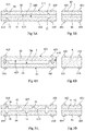
- FIGS. 3A and 3B are very simplified views, respectively a cross-section and a side view, of another embodiment of a chip assembly.
- FIGS. 3A, 3B as well as in the following drawings, the chips have not been detailed and only the chips, the binder layer, and the contacts have been illustrated.
- sawing or cutting lines 72 are provided in the back sides of chips 62 and 64 .
- the lines are for example formed on cutting of the chips to individualize wafers from which they are manufactured. It should be noted that this embodiment is compatible with an assembly in full wafers by having previously formed lines 72 in the back sides of the respective wafers. Once chips 62 and 64 have been assembled back to back, here, preferably by glue to fill the sawing lines, the external aspect of the obtained assembly 6 is similar to that having no lines ( FIG. 2 ).
- the advantage of sawing lines 72 is to embrittle the chips if a pirate attempts to separate them. The chip breakage is thus favored in case of an attack.
- lines 72 depend on the desired size and brittleness. Further, in the case where the chip comprises a ground plane on the back side, lines 72 will preferably be formed at the chip periphery. Lines 72 have been shown vertically above one another, which improves the assembly and enables to compensate, over the formed assembly, for the brittleness individually brought to each chip. It may however be provided for lines 72 not to be, or to only partially be, vertically above one another.
- FIGS. 4A and 4B are very simplified views, respectively a cross-section and a side view, of another embodiment of a chip assembly.
- a cavity 74 is formed in back side 643 of chip 64 .
- Cavity 74 is only present in the central portion of the chip, that is, back side 643 comprises a peripheral edge 649 .
- Edge 649 is intended to bear against back side 623 of the other chip (here 62 ) and the cavity is intended to be filled with binder 7 (for example, with glue).
- binder 7 for example, with glue
- FIGS. 5A and 5B are very simplified views, respectively a cross-section and a side view, of another embodiment of a chip assembly.
- trenches 76 are formed from their respective back sides.
- the function of these trenches is, like for sawing lines 72 ( FIG. 4A ), to embrittle the chips to favor their breakage in case of an attack.
- the trenches 76 of a chip may or not be vertically above the trenches of the other chip.
- An advantage of the described embodiments is that they prevent an upstream attack, that is, an attack attempt to separate the chips generates a destruction thereof and thus makes the attack inoperative.
- An advantage of the described embodiments is that they require no modification of the actual chip and in particular no modification of the components and circuits formed inside, on top of, and from the front side.
- An advantage of the described embodiments is that their implementation is independent from the manufacturing of the actual chips.
- the chips may comprise back-side attack detection circuits such as, for example, conductive vias coupling the back side to front side detection circuits, resistive detection networks and, more generally, any usual circuit.
Abstract
Description
Claims (10)
Priority Applications (2)
| Application Number | Priority Date | Filing Date | Title |
|---|---|---|---|
| US17/466,941 US11640946B2 (en) | 2018-05-18 | 2021-09-03 | Protection of integrated circuits |
| US18/128,044 US20230245984A1 (en) | 2018-05-18 | 2023-03-29 | Protection of integrated circuits |
Applications Claiming Priority (2)
| Application Number | Priority Date | Filing Date | Title |
|---|---|---|---|
| FR1854155 | 2018-05-18 | ||
| FR1854155 | 2018-05-18 |
Related Child Applications (1)
| Application Number | Title | Priority Date | Filing Date |
|---|---|---|---|
| US17/466,941 Division US11640946B2 (en) | 2018-05-18 | 2021-09-03 | Protection of integrated circuits |
Publications (2)
| Publication Number | Publication Date |
|---|---|
| US20190355674A1 US20190355674A1 (en) | 2019-11-21 |
| US11139255B2 true US11139255B2 (en) | 2021-10-05 |
Family
ID=63963092
Family Applications (3)
| Application Number | Title | Priority Date | Filing Date |
|---|---|---|---|
| US16/411,960 Active US11139255B2 (en) | 2018-05-18 | 2019-05-14 | Protection of integrated circuits |
| US17/466,941 Active 2039-07-16 US11640946B2 (en) | 2018-05-18 | 2021-09-03 | Protection of integrated circuits |
| US18/128,044 Pending US20230245984A1 (en) | 2018-05-18 | 2023-03-29 | Protection of integrated circuits |
Family Applications After (2)
| Application Number | Title | Priority Date | Filing Date |
|---|---|---|---|
| US17/466,941 Active 2039-07-16 US11640946B2 (en) | 2018-05-18 | 2021-09-03 | Protection of integrated circuits |
| US18/128,044 Pending US20230245984A1 (en) | 2018-05-18 | 2023-03-29 | Protection of integrated circuits |
Country Status (1)
| Country | Link |
|---|---|
| US (3) | US11139255B2 (en) |
Families Citing this family (1)
| Publication number | Priority date | Publication date | Assignee | Title |
|---|---|---|---|---|
| CN111834438A (en) * | 2019-04-18 | 2020-10-27 | 西部数据技术公司 | Aperture structure on backside of semiconductor component for mitigating delamination in stacked package |
Citations (10)
| Publication number | Priority date | Publication date | Assignee | Title |
|---|---|---|---|---|
| US20030122237A1 (en) * | 2001-12-28 | 2003-07-03 | Yoshihiro Saeki | Semiconductor device |
| US20030148597A1 (en) * | 2002-01-09 | 2003-08-07 | Tan Hock Chuan | Stacked die in die BGA package |
| US20030153122A1 (en) * | 2002-02-13 | 2003-08-14 | Michael Brooks | Methods and apparatus for a stacked-die interposer |
| US20040026768A1 (en) * | 2002-08-08 | 2004-02-12 | Taar Reginald T. | Semiconductor dice with edge cavities |
| US20090026592A1 (en) * | 2007-07-24 | 2009-01-29 | Micron Technology, Inc. | Semiconductor dies with recesses, associated leadframes, and associated systems and methods |
| US20090091042A1 (en) * | 2007-10-04 | 2009-04-09 | Byung Tai Do | Integrated circuit package system including die having relieved active region |
| TWI331379B (en) | 2007-04-17 | 2010-10-01 | Powertech Technology Inc | Back-to-back chip stacked device |
| WO2012087580A2 (en) | 2010-12-24 | 2012-06-28 | Io Semiconductor, Inc. | Trap rich layer for semiconductor devices |
| US20180033846A1 (en) * | 2011-10-14 | 2018-02-01 | Diftek Lasers, Inc. | Electronic device and method of making thereof |
| US20200075501A1 (en) * | 2016-03-31 | 2020-03-05 | Intel Corporation | Electromagnetic interference shielding for semiconductor packages using bond wires |
Family Cites Families (1)
| Publication number | Priority date | Publication date | Assignee | Title |
|---|---|---|---|---|
| US20130044431A1 (en) * | 2011-08-18 | 2013-02-21 | Harris Corporation | Liquid cooling of stacked die through substrate lamination |
-
2019
- 2019-05-14 US US16/411,960 patent/US11139255B2/en active Active
-
2021
- 2021-09-03 US US17/466,941 patent/US11640946B2/en active Active
-
2023
- 2023-03-29 US US18/128,044 patent/US20230245984A1/en active Pending
Patent Citations (10)
| Publication number | Priority date | Publication date | Assignee | Title |
|---|---|---|---|---|
| US20030122237A1 (en) * | 2001-12-28 | 2003-07-03 | Yoshihiro Saeki | Semiconductor device |
| US20030148597A1 (en) * | 2002-01-09 | 2003-08-07 | Tan Hock Chuan | Stacked die in die BGA package |
| US20030153122A1 (en) * | 2002-02-13 | 2003-08-14 | Michael Brooks | Methods and apparatus for a stacked-die interposer |
| US20040026768A1 (en) * | 2002-08-08 | 2004-02-12 | Taar Reginald T. | Semiconductor dice with edge cavities |
| TWI331379B (en) | 2007-04-17 | 2010-10-01 | Powertech Technology Inc | Back-to-back chip stacked device |
| US20090026592A1 (en) * | 2007-07-24 | 2009-01-29 | Micron Technology, Inc. | Semiconductor dies with recesses, associated leadframes, and associated systems and methods |
| US20090091042A1 (en) * | 2007-10-04 | 2009-04-09 | Byung Tai Do | Integrated circuit package system including die having relieved active region |
| WO2012087580A2 (en) | 2010-12-24 | 2012-06-28 | Io Semiconductor, Inc. | Trap rich layer for semiconductor devices |
| US20180033846A1 (en) * | 2011-10-14 | 2018-02-01 | Diftek Lasers, Inc. | Electronic device and method of making thereof |
| US20200075501A1 (en) * | 2016-03-31 | 2020-03-05 | Intel Corporation | Electromagnetic interference shielding for semiconductor packages using bond wires |
Non-Patent Citations (1)
| Title |
|---|
| INPI Search Report and Written Opinion for FR 1854155 dated Dec. 10, 2018 (8 pages). |
Also Published As
| Publication number | Publication date |
|---|---|
| US20190355674A1 (en) | 2019-11-21 |
| US11640946B2 (en) | 2023-05-02 |
| US20210398919A1 (en) | 2021-12-23 |
| US20230245984A1 (en) | 2023-08-03 |
Similar Documents
| Publication | Publication Date | Title |
|---|---|---|
| KR101264926B1 (en) | Method of manufacturing semiconductor device and semiconductor device | |
| US8456020B2 (en) | Semiconductor package and method of manufacturing the same | |
| EP2291858B1 (en) | Packaged semiconductor product and method for manufacture thereof | |
| JP5279180B2 (en) | Semiconductor device | |
| US6420208B1 (en) | Method of forming an alternative ground contact for a semiconductor die | |
| US20230245984A1 (en) | Protection of integrated circuits | |
| JP2010129958A (en) | Semiconductor device, and manufacturing method thereof | |
| WO2014162795A1 (en) | Esd protective device | |
| KR100660882B1 (en) | Board on chip package and manufacturing method thereof | |
| US6133625A (en) | Semiconductor device and method for manufacturing the same | |
| JP3529050B2 (en) | Method for manufacturing semiconductor device | |
| US7649250B2 (en) | Semiconductor package | |
| US20080014679A1 (en) | Packaging structure with protective layers and packaging method thereof | |
| US20120225501A1 (en) | Three dimensional semiconductor device, method of manufacturing the same and electrical cutoff method for using fuse pattern of the same | |
| KR100805503B1 (en) | Semiconductor device, method for manufacturing the same, circuit board and electronic apparatus | |
| US20090134494A1 (en) | Semiconductor device and method of manufacturing the same | |
| US20070284702A1 (en) | Semiconductor device having a bonding pad and fuse and method for forming the same | |
| US10283483B2 (en) | Packaging method and package structure for image sensing chip | |
| US6581279B1 (en) | Method of collectively packaging electronic components | |
| US7696615B2 (en) | Semiconductor device having pillar-shaped terminal | |
| US20040089930A1 (en) | Simplified stacked chip assemblies | |
| KR20110136297A (en) | Stack type semiconductor package | |
| CN109950220B (en) | Bonding pad structure and manufacturing method thereof | |
| JP5106763B2 (en) | Semiconductor device | |
| JP6311849B1 (en) | Semiconductor component and method for manufacturing semiconductor component |
Legal Events
| Date | Code | Title | Description |
|---|---|---|---|
| AS | Assignment |
Owner name: STMICROELECTRONICS (GRENOBLE 2) SAS, FRANCE Free format text: ASSIGNMENT OF ASSIGNORS INTEREST;ASSIGNORS:COFFY, ROMAIN;RIVIERE, JEAN-MICHEL;REEL/FRAME:049176/0159 Effective date: 20190318 Owner name: STMICROELECTRONICS (ROUSSET) SAS, FRANCE Free format text: ASSIGNMENT OF ASSIGNORS INTEREST;ASSIGNOR:FARISON, DENIS;REEL/FRAME:049176/0110 Effective date: 20190509 |
|
| FEPP | Fee payment procedure |
Free format text: ENTITY STATUS SET TO UNDISCOUNTED (ORIGINAL EVENT CODE: BIG.); ENTITY STATUS OF PATENT OWNER: LARGE ENTITY |
|
| STPP | Information on status: patent application and granting procedure in general |
Free format text: NON FINAL ACTION MAILED |
|
| STPP | Information on status: patent application and granting procedure in general |
Free format text: RESPONSE TO NON-FINAL OFFICE ACTION ENTERED AND FORWARDED TO EXAMINER |
|
| STPP | Information on status: patent application and granting procedure in general |
Free format text: FINAL REJECTION MAILED |
|
| STPP | Information on status: patent application and granting procedure in general |
Free format text: RESPONSE AFTER FINAL ACTION FORWARDED TO EXAMINER |
|
| STPP | Information on status: patent application and granting procedure in general |
Free format text: NOTICE OF ALLOWANCE MAILED -- APPLICATION RECEIVED IN OFFICE OF PUBLICATIONS |
|
| STPP | Information on status: patent application and granting procedure in general |
Free format text: PUBLICATIONS -- ISSUE FEE PAYMENT RECEIVED |
|
| STPP | Information on status: patent application and granting procedure in general |
Free format text: PUBLICATIONS -- ISSUE FEE PAYMENT VERIFIED |
|
| STCF | Information on status: patent grant |
Free format text: PATENTED CASE |