US11137296B2 - Force sensor with MEMS-based device and force touching member - Google Patents
Force sensor with MEMS-based device and force touching member Download PDFInfo
- Publication number
- US11137296B2 US11137296B2 US16/426,463 US201916426463A US11137296B2 US 11137296 B2 US11137296 B2 US 11137296B2 US 201916426463 A US201916426463 A US 201916426463A US 11137296 B2 US11137296 B2 US 11137296B2
- Authority
- US
- United States
- Prior art keywords
- force
- mems
- rod
- touching member
- package body
- Prior art date
- Legal status (The legal status is an assumption and is not a legal conclusion. Google has not performed a legal analysis and makes no representation as to the accuracy of the status listed.)
- Active
Links
Images


Classifications
-
- B—PERFORMING OPERATIONS; TRANSPORTING
- B81—MICROSTRUCTURAL TECHNOLOGY
- B81B—MICROSTRUCTURAL DEVICES OR SYSTEMS, e.g. MICROMECHANICAL DEVICES
- B81B3/00—Devices comprising flexible or deformable elements, e.g. comprising elastic tongues or membranes
- B81B3/0064—Constitution or structural means for improving or controlling the physical properties of a device
- B81B3/0067—Mechanical properties
- B81B3/0072—For controlling internal stress or strain in moving or flexible elements, e.g. stress compensating layers
-
- G—PHYSICS
- G01—MEASURING; TESTING
- G01L—MEASURING FORCE, STRESS, TORQUE, WORK, MECHANICAL POWER, MECHANICAL EFFICIENCY, OR FLUID PRESSURE
- G01L1/00—Measuring force or stress, in general
- G01L1/14—Measuring force or stress, in general by measuring variations in capacitance or inductance of electrical elements, e.g. by measuring variations of frequency of electrical oscillators
- G01L1/142—Measuring force or stress, in general by measuring variations in capacitance or inductance of electrical elements, e.g. by measuring variations of frequency of electrical oscillators using capacitors
-
- B—PERFORMING OPERATIONS; TRANSPORTING
- B81—MICROSTRUCTURAL TECHNOLOGY
- B81B—MICROSTRUCTURAL DEVICES OR SYSTEMS, e.g. MICROMECHANICAL DEVICES
- B81B2203/00—Basic microelectromechanical structures
- B81B2203/03—Static structures
- B81B2203/0369—Static structures characterized by their profile
- B81B2203/0376—Static structures characterized by their profile rounded profile
-
- B—PERFORMING OPERATIONS; TRANSPORTING
- B81—MICROSTRUCTURAL TECHNOLOGY
- B81B—MICROSTRUCTURAL DEVICES OR SYSTEMS, e.g. MICROMECHANICAL DEVICES
- B81B2203/00—Basic microelectromechanical structures
- B81B2203/03—Static structures
- B81B2203/0369—Static structures characterized by their profile
- B81B2203/0392—Static structures characterized by their profile profiles not provided for in B81B2203/0376 - B81B2203/0384
-
- H—ELECTRICITY
- H01—ELECTRIC ELEMENTS
- H01L—SEMICONDUCTOR DEVICES NOT COVERED BY CLASS H10
- H01L2224/00—Indexing scheme for arrangements for connecting or disconnecting semiconductor or solid-state bodies and methods related thereto as covered by H01L24/00
- H01L2224/01—Means for bonding being attached to, or being formed on, the surface to be connected, e.g. chip-to-package, die-attach, "first-level" interconnects; Manufacturing methods related thereto
- H01L2224/42—Wire connectors; Manufacturing methods related thereto
- H01L2224/47—Structure, shape, material or disposition of the wire connectors after the connecting process
- H01L2224/48—Structure, shape, material or disposition of the wire connectors after the connecting process of an individual wire connector
- H01L2224/4805—Shape
- H01L2224/4809—Loop shape
- H01L2224/48091—Arched
Definitions
- the present invention relates to a force sensor, particularly to a force sensor allowing a greater assembly tolerance.
- a MEMS-based device includes a mobile MEMS component.
- the function of a MEMS-based device may be realized through measuring the physical magnitude of the movement of the MEMS component.
- the force sensor is an example of MEMS devices, able to detect a pressing action and/or a pressing force.
- the existing force sensors include the piezoresistor type pressure sensor and the capacitor type pressure sensor.
- FIG. 1 In a conventional piezoresistor type pressure sensor, a plurality of piezoresistors 12 is disposed on a mobile membrane 11 . While a pressing force causes the mobile membrane 11 to deform, the piezoresistors 12 generate corresponding signals.
- FIG. 2 A conventional capacitor type pressure sensor includes a mobile membrane 21 and a fixed electrode 22 , and the mobile membrane 21 is disposed opposite to the fixed electrode 22 , whereby is formed a sensing capacitor. The signals generated by the sensing capacitor are transmitted to an Application Specific Integrated Circuit (ASIC) chip (not shown in the drawing) through a lead and processed by the ASIC chip. It is easily understood: a package body 23 is needed to package and protect the abovementioned components. A pressing force is conducted through the package body 23 to cause the deformation of the mobile membrane 21 and make the sensing capacitor output corresponding signals.
- ASIC Application Specific Integrated Circuit
- the pressure sensor will output different sensation signals respectively according to the contact positions. For example, as the contact position of the force F 1 is nearer to the center of the pressure sensor, the mobile membrane 11 will generate a greater deformation. Thus, the pressure sensor outputs a greater sensation signal.
- the contact positions of the force F 2 and the force F 3 are farther from the center of the pressure sensor. Even though the forces F 2 and F 3 are identical to the force F 1 , they cause smaller deformations of the mobile membrane 11 and generate smaller output sensation signals. The fact that the forces of the same magnitude generate different output sensation signals is unfavorable to the succeeding processing and treatment of the signals.
- a force sensor is provided therein, wherein a force touching member is disposed on the package body opposite to the MEMS-based device, whereby the contact of a pressing element and the force touching member makes the pressing force concentrated on the force touching member, wherefore the force sensor of the present invention can endure a greater assembly tolerance.
- the force sensor of the present invention comprises a package substrate, a MEMS-based device, a package body and a force touching member.
- the MEMS-based device is disposed on the package substrate and electrically connected with the package substrate.
- the package body encapsulates the MEMS-based device.
- the force touching member includes a rod, disposed on the package body and corresponding to the MEMS-based device.
- FIG. 2 is a diagram schematically showing a conventional capacitor type pressure sensor
- FIG. 3 is a diagram schematically showing the output signals corresponding to different contact positions of a conventional force sensor
- FIG. 4 is a diagram schematically showing a force sensor according to a first embodiment of the present invention.
- FIG. 5 is a diagram schematically showing the output signals corresponding to different contact positions of the force sensor of the present invention.
- FIG. 6 is a diagram schematically showing a force sensor according to a second embodiment of the present invention.
- FIG. 7 is a diagram schematically showing a force sensor according to a third embodiment of the present invention.
- FIG. 8 is a diagram schematically showing a force sensor according to a fourth embodiment of the present invention.
- FIG. 9 is a diagram schematically showing a force sensor according to a fifth embodiment of the present invention.
- FIG. 12 is a diagram schematically showing a force sensor according to a seventh embodiment of the present invention.
- FIG. 13 is a diagram schematically showing the projection dimensions of the features illustrated in FIG. 4 .
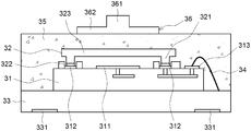
- a force sensor includes a package substrate 33 , a MEMS-based device, a package body 35 and a force touching member 36 .
- the MEMS-based device is disposed on the package substrate 33 and electrically connected with the package substrate 33 .
- the MEMS-based device includes a first substrate 31 and a second substrate 32 , wherein the first substrate 31 includes a fixed electrode 311 , a first conductive contact 312 and a second conductive contact 313 .
- the first substrate 31 has a plurality of metal layers, which are connected with each other by interconnection structures to form the desired circuit.
- the first substrate 31 includes a driver circuit and/or a sensing circuit.
- the first substrate 31 may have an analog and/or digital circuit, which is normally realized by an Application Specific Integrated Circuit (ASIC).
- ASIC Application Specific Integrated Circuit
- the present invention is not limited by the abovementioned embodiments.
- the first substrate 31 is also called the electrode substrate.
- the first substrate 31 may be a substrate having appropriate rigidity, such as a complementary metal oxide semiconductor (CMOS) substrate or a glass substrate.
- CMOS complementary metal oxide semiconductor
- the second substrate 32 has a first surface (i.e. the surface of the second substrate 32 , which faces downward), a second surface opposite to the first surface, and a microelectromechanical system (MEMS) element 323 .
- the second substrate 32 is disposed over the first substrate 31 with the first surface being faced to the first substrate 31 and electrically connected with the first conductive contact 312 of the first substrate 31 .
- at least one second connection member 321 of the second substrate 32 and a conductive material 322 on the terminal of the second connection member 321 are connected with the first conductive contact 312 of the first substrate 31 .
- the MEMS-based device which is formed via joining the first substrate 31 with the second substrate 32 , is disposed on the package substrate 33 ; a wire bonding process uses a lead 34 to electrically connect the second conductive contact 313 of the first substrate 31 with the package substrate 33 ; the package body 35 is used to encapsulate the MEMS-based device and the lead 34 for protecting the abovementioned elements.
- the MEMS-based device which is encapsulated by the package body 35 , can be electrically connected with the external device through the second conductive contact 313 of the first substrate 31 and at least one external conductive contact 331 of the package substrate 33 .
- the force touching member 36 is disposed on the package body 35 and sticking out of the package body 35 .
- the force touching member 36 includes a single rod 361 , which is corresponding to the MEMS-based device.
- the single rod 361 of the force touching member 36 is corresponding to the MEMS element 323 and just right on the MEMS element 323 .
- the rod 361 of the force touching member 36 is corresponding to the deformable area of the MEMS element 323 and just right on the deformable area of the MEMS element 323 .
- the single rod 361 of the force touching member 36 is corresponding to the geometric center of the deformable area of the MEMS element 323 . Refer to FIG. 4 and FIG. 5 .
- Different assembly errors may result in different deviations, such as the pressing elements A 1 , A 2 and A 3 in FIG. 4 .
- the pressing force is concentrated on the force touching member 36 .
- the force sensor of the present invention can still output consistent sensation signals even though different assembly errors result in different deviations, as shown in FIG. 5 .
- the top surface of the rod 361 is a planar surface.
- the present invention is not limited by the embodiment. Refer to FIG. 6 .
- the top surface of the force touching member 36 is a curved surface. It is easily understood: the rod 361 may be stuck to the package body 35 by an adhesive material 37 .
- the force touching member may be an extension of the package body 35 , such as the protruding portion 351 in FIG. 7 .
- the protruding portion 351 is corresponding to the MEMS-based device. More specifically, the protruding portion 351 is corresponding to the deformable area of the MEMS element 323 and just right on the deformable area of the MEMS element 323 . In one embodiment, the protruding portion 351 is corresponding to the geometric center of the deformable area of the MEMS element 323 .
- the force touching member 36 includes a rod 361 and a plate 362 , wherein the plate 362 is interposed between the rod 361 and the package body 35 .
- the force touching member 36 is an integral element.
- the rod 361 and the plate 362 are fabricated into a one-piece element.
- the force touching member 36 is made of a metallic material.
- the projection area of the plate 362 may be equal to or smaller than the deformable area of the MEMS element 323 .
- the plate 362 is corresponding to the deformable area the MEMS element 323 . Refer to FIG. 9 .
- the projection area of the plate 362 is larger than the MEMS-based device and covers the upper surface of the package body 35 .
- the top surface of the rod 361 may be a planar surface (as shown in FIG. 8 ) or a curved surface (as shown in FIG. 9 ). It should be explained: the measurement range of the force sensor of the present invention, such as a measurement range of up to 10 Newtons or 100 Newtons, can be adjusted via modifying the thickness of the MEMS element 323 or modifying the thickness/material of the package body 35 ; the measurement range of the force sensor of the present invention can be also controlled via modifying the thickness of the plate 323 .
- the plate 362 may be disposed above the rod 361 .
- the rod 361 is interposed between the plate 362 and the package body 35 .
- the plate 362 further includes at least one connection leg 363 , which is connected to the package body 35 , whereby to prevent the plate 362 from being tilted during pressing.
- the rod 361 may be formed via dispensing a resin on the package body 35 . It is easily understood: the rod 361 is made of a polymeric material in this embodiment.
- the present invention is characterized in that a force touching member is disposed on the package body corresponding to the MEMS-based device and that the contact of the pressing element and the force touching member makes the force, which is originally applied to the pressing element, be concentrated on the force touching member.
- the force touching member may include a plate.
- the measurement range of the force sensor of the present invention can be controlled via modifying the thickness of the plate.
Landscapes
- Engineering & Computer Science (AREA)
- Power Engineering (AREA)
- Physics & Mathematics (AREA)
- General Physics & Mathematics (AREA)
- Mechanical Engineering (AREA)
- Computer Hardware Design (AREA)
- Microelectronics & Electronic Packaging (AREA)
- Micromachines (AREA)
- Force Measurement Appropriate To Specific Purposes (AREA)
Abstract
Description
Claims (8)
Applications Claiming Priority (2)
| Application Number | Priority Date | Filing Date | Title |
|---|---|---|---|
| CN201810537745.XA CN110553761A (en) | 2018-05-30 | 2018-05-30 | Force sensor |
| CN201810537745.X | 2018-05-30 |
Publications (2)
| Publication Number | Publication Date |
|---|---|
| US20190368951A1 US20190368951A1 (en) | 2019-12-05 |
| US11137296B2 true US11137296B2 (en) | 2021-10-05 |
Family
ID=68693224
Family Applications (1)
| Application Number | Title | Priority Date | Filing Date |
|---|---|---|---|
| US16/426,463 Active US11137296B2 (en) | 2018-05-30 | 2019-05-30 | Force sensor with MEMS-based device and force touching member |
Country Status (3)
| Country | Link |
|---|---|
| US (1) | US11137296B2 (en) |
| CN (1) | CN110553761A (en) |
| TW (1) | TWI692623B (en) |
Citations (6)
| Publication number | Priority date | Publication date | Assignee | Title |
|---|---|---|---|---|
| US8154115B1 (en) * | 2010-12-17 | 2012-04-10 | Siliconware Precision Industries Co., Ltd. | Package structure having MEMS element and fabrication method thereof |
| US20130127001A1 (en) * | 2011-11-11 | 2013-05-23 | Xintec Inc. | Semiconductor package and method of fabricating the same |
| US20150259196A1 (en) * | 2014-03-13 | 2015-09-17 | Kabushiki Kaisha Toshiba | Mems device and method of manufacturing the same |
| US20170343430A1 (en) * | 2016-05-31 | 2017-11-30 | Stmicroelectronics S.R.L. | Miniaturized load sensor device having low sensitivity to thermo-mechanical packaging stress, in particular force and pressure sensor |
| US20180086626A1 (en) * | 2016-09-26 | 2018-03-29 | MEAS Switzerland S.a.r.l. | Method of manufacturing a sensor |
| US20190330053A1 (en) * | 2018-04-27 | 2019-10-31 | Miramems Sensing Technology Co., Ltd | Force sensor and manufacture method thereof |
Family Cites Families (12)
| Publication number | Priority date | Publication date | Assignee | Title |
|---|---|---|---|---|
| CN2156491Y (en) * | 1992-12-24 | 1994-02-16 | 孟繁英 | Force sensor |
| KR20040060849A (en) * | 2001-04-13 | 2004-07-06 | 쓰리엠 이노베이티브 프로퍼티즈 컴파니 | Touch screen with rotationally isolated force sensor |
| CN1239893C (en) * | 2002-09-10 | 2006-02-01 | 祥群科技股份有限公司 | Condenser type pressure micro sensing element and fingerprint reading chip applied thereby |
| JP4907050B2 (en) * | 2003-03-31 | 2012-03-28 | 株式会社ワコー | Force detection device |
| CN1308886C (en) * | 2004-02-05 | 2007-04-04 | 祥群科技股份有限公司 | Capacitance type pressure sensing element structure and mfg. method |
| CN201464094U (en) * | 2009-07-07 | 2010-05-12 | 曹勤华 | Tensile compression type fixed strut-beam force sensor |
| CN201464093U (en) * | 2009-07-07 | 2010-05-12 | 曹勤华 | Multi-clamped-beam circular membrane type force sensor |
| US7972888B1 (en) * | 2010-03-11 | 2011-07-05 | Memsensing Microsystems Technology Co., Ltd. | Methods for manufacturing MEMS sensor and thin film and cantilever beam thereof with epitaxial growth process |
| US9267857B2 (en) * | 2014-01-07 | 2016-02-23 | Honeywell International Inc. | Pressure sensor having a bossed diaphragm |
| TWI538113B (en) * | 2014-02-14 | 2016-06-11 | 南茂科技股份有限公司 | Micro electro mechanical systems package and manufacturing method thereof |
| CN108344530A (en) * | 2017-01-24 | 2018-07-31 | 英属开曼群岛商智动全球股份有限公司 | Strength sensor |
| CN108036879B (en) * | 2017-12-15 | 2020-02-18 | 广州智能装备研究院有限公司 | Capacitive flexible touch sensor and manufacturing method thereof |
-
2018
- 2018-05-30 CN CN201810537745.XA patent/CN110553761A/en active Pending
-
2019
- 2019-05-28 TW TW108118452A patent/TWI692623B/en active
- 2019-05-30 US US16/426,463 patent/US11137296B2/en active Active
Patent Citations (6)
| Publication number | Priority date | Publication date | Assignee | Title |
|---|---|---|---|---|
| US8154115B1 (en) * | 2010-12-17 | 2012-04-10 | Siliconware Precision Industries Co., Ltd. | Package structure having MEMS element and fabrication method thereof |
| US20130127001A1 (en) * | 2011-11-11 | 2013-05-23 | Xintec Inc. | Semiconductor package and method of fabricating the same |
| US20150259196A1 (en) * | 2014-03-13 | 2015-09-17 | Kabushiki Kaisha Toshiba | Mems device and method of manufacturing the same |
| US20170343430A1 (en) * | 2016-05-31 | 2017-11-30 | Stmicroelectronics S.R.L. | Miniaturized load sensor device having low sensitivity to thermo-mechanical packaging stress, in particular force and pressure sensor |
| US20180086626A1 (en) * | 2016-09-26 | 2018-03-29 | MEAS Switzerland S.a.r.l. | Method of manufacturing a sensor |
| US20190330053A1 (en) * | 2018-04-27 | 2019-10-31 | Miramems Sensing Technology Co., Ltd | Force sensor and manufacture method thereof |
Also Published As
| Publication number | Publication date |
|---|---|
| CN110553761A (en) | 2019-12-10 |
| TWI692623B (en) | 2020-05-01 |
| US20190368951A1 (en) | 2019-12-05 |
| TW202004142A (en) | 2020-01-16 |
Similar Documents
| Publication | Publication Date | Title |
|---|---|---|
| US10486962B2 (en) | Force sensor and manufacture method thereof | |
| US11946817B2 (en) | Integrated digital force sensors and related methods of manufacture | |
| US8806964B2 (en) | Force sensor | |
| US9032818B2 (en) | Microelectromechanical load sensor and methods of manufacturing the same | |
| US20120152037A1 (en) | Force sensor | |
| EP2270455A2 (en) | Force sensor apparatus | |
| US20240133755A1 (en) | Temperature coefficient of offset compensation for force sensor and strain gauge | |
| US10538428B2 (en) | MEMS device and method for manufacturing the same | |
| US11137296B2 (en) | Force sensor with MEMS-based device and force touching member | |
| US10732057B2 (en) | Low cost overmolded leadframe force sensor with multiple mounting positions | |
| KR101573367B1 (en) | Piezoresistive typed ceramic pressure sensor | |
| TWI718373B (en) | Force sensor and manufacture method thereof | |
| US10266391B2 (en) | Microelectromechanical system device | |
| JP6122345B6 (en) | Manufacturing method of pressure sensor | |
| JP6122345B2 (en) | Manufacturing method of pressure sensor |
Legal Events
| Date | Code | Title | Description |
|---|---|---|---|
| FEPP | Fee payment procedure |
Free format text: ENTITY STATUS SET TO UNDISCOUNTED (ORIGINAL EVENT CODE: BIG.); ENTITY STATUS OF PATENT OWNER: LARGE ENTITY |
|
| AS | Assignment |
Owner name: MIRAMEMS SENSING TECHNOLOGY CO., LTD, CHINA Free format text: ASSIGNMENT OF ASSIGNORS INTEREST;ASSIGNORS:TSENG, LI-TIEN;CHIEN, YU-HAO;KUO, CHIH-LIANG;AND OTHERS;REEL/FRAME:049394/0756 Effective date: 20190528 |
|
| STPP | Information on status: patent application and granting procedure in general |
Free format text: DOCKETED NEW CASE - READY FOR EXAMINATION |
|
| AS | Assignment |
Owner name: MIRAMEMS SENSING TECHNOLOGY CO., LTD, CHINA Free format text: CHANGE OF ADDRESS;ASSIGNOR:MIRAMEMS SENSING TECHNOLOGY CO., LTD;REEL/FRAME:051897/0368 Effective date: 20170725 |
|
| STPP | Information on status: patent application and granting procedure in general |
Free format text: NON FINAL ACTION MAILED |
|
| STPP | Information on status: patent application and granting procedure in general |
Free format text: DOCKETED NEW CASE - READY FOR EXAMINATION |
|
| STPP | Information on status: patent application and granting procedure in general |
Free format text: NON FINAL ACTION MAILED |
|
| STPP | Information on status: patent application and granting procedure in general |
Free format text: RESPONSE TO NON-FINAL OFFICE ACTION ENTERED AND FORWARDED TO EXAMINER |
|
| STPP | Information on status: patent application and granting procedure in general |
Free format text: NOTICE OF ALLOWANCE MAILED -- APPLICATION RECEIVED IN OFFICE OF PUBLICATIONS |
|
| STPP | Information on status: patent application and granting procedure in general |
Free format text: PUBLICATIONS -- ISSUE FEE PAYMENT VERIFIED |
|
| STCF | Information on status: patent grant |
Free format text: PATENTED CASE |