US11101385B2 - Fin field effect transistor (FinFET) device structure with air gap and method for forming the same - Google Patents
Fin field effect transistor (FinFET) device structure with air gap and method for forming the same Download PDFInfo
- Publication number
- US11101385B2 US11101385B2 US16/135,108 US201816135108A US11101385B2 US 11101385 B2 US11101385 B2 US 11101385B2 US 201816135108 A US201816135108 A US 201816135108A US 11101385 B2 US11101385 B2 US 11101385B2
- Authority
- US
- United States
- Prior art keywords
- spacer
- mask layer
- finfet
- spacers
- device structure
- Prior art date
- Legal status (The legal status is an assumption and is not a legal conclusion. Google has not performed a legal analysis and makes no representation as to the accuracy of the status listed.)
- Active, expires
Links
Images


Classifications
-
- H01L29/7851—
-
- H—ELECTRICITY
- H10—SEMICONDUCTOR DEVICES; ELECTRIC SOLID-STATE DEVICES NOT OTHERWISE PROVIDED FOR
- H10D—INORGANIC ELECTRIC SEMICONDUCTOR DEVICES
- H10D62/00—Semiconductor bodies, or regions thereof, of devices having potential barriers
- H10D62/10—Shapes, relative sizes or dispositions of the regions of the semiconductor bodies; Shapes of the semiconductor bodies
- H10D62/13—Semiconductor regions connected to electrodes carrying current to be rectified, amplified or switched, e.g. source or drain regions
- H10D62/149—Source or drain regions of field-effect devices
- H10D62/151—Source or drain regions of field-effect devices of IGFETs
-
- H—ELECTRICITY
- H01—ELECTRIC ELEMENTS
- H01L—SEMICONDUCTOR DEVICES NOT COVERED BY CLASS H10
- H01L21/00—Processes or apparatus adapted for the manufacture or treatment of semiconductor or solid state devices or of parts thereof
- H01L21/02—Manufacture or treatment of semiconductor devices or of parts thereof
- H01L21/027—Making masks on semiconductor bodies for further photolithographic processing not provided for in group H01L21/18 or H01L21/34
- H01L21/033—Making masks on semiconductor bodies for further photolithographic processing not provided for in group H01L21/18 or H01L21/34 comprising inorganic layers
- H01L21/0334—Making masks on semiconductor bodies for further photolithographic processing not provided for in group H01L21/18 or H01L21/34 comprising inorganic layers characterised by their size, orientation, disposition, behaviour, shape, in horizontal or vertical plane
- H01L21/0337—Making masks on semiconductor bodies for further photolithographic processing not provided for in group H01L21/18 or H01L21/34 comprising inorganic layers characterised by their size, orientation, disposition, behaviour, shape, in horizontal or vertical plane characterised by the process involved to create the mask, e.g. lift-off masks, sidewalls, or to modify the mask, e.g. pre-treatment, post-treatment
-
- H—ELECTRICITY
- H01—ELECTRIC ELEMENTS
- H01L—SEMICONDUCTOR DEVICES NOT COVERED BY CLASS H10
- H01L21/00—Processes or apparatus adapted for the manufacture or treatment of semiconductor or solid state devices or of parts thereof
- H01L21/70—Manufacture or treatment of devices consisting of a plurality of solid state components formed in or on a common substrate or of parts thereof; Manufacture of integrated circuit devices or of parts thereof
- H01L21/71—Manufacture of specific parts of devices defined in group H01L21/70
- H01L21/768—Applying interconnections to be used for carrying current between separate components within a device comprising conductors and dielectrics
- H01L21/76801—Applying interconnections to be used for carrying current between separate components within a device comprising conductors and dielectrics characterised by the formation and the after-treatment of the dielectrics, e.g. smoothing
- H01L21/76829—Applying interconnections to be used for carrying current between separate components within a device comprising conductors and dielectrics characterised by the formation and the after-treatment of the dielectrics, e.g. smoothing characterised by the formation of thin functional dielectric layers, e.g. dielectric etch-stop, barrier, capping or liner layers
-
- H01L21/823418—
-
- H01L21/823431—
-
- H01L21/823468—
-
- H01L29/0649—
-
- H01L29/66545—
-
- H01L29/66795—
-
- H—ELECTRICITY
- H10—SEMICONDUCTOR DEVICES; ELECTRIC SOLID-STATE DEVICES NOT OTHERWISE PROVIDED FOR
- H10D—INORGANIC ELECTRIC SEMICONDUCTOR DEVICES
- H10D30/00—Field-effect transistors [FET]
- H10D30/01—Manufacture or treatment
- H10D30/021—Manufacture or treatment of FETs having insulated gates [IGFET]
- H10D30/024—Manufacture or treatment of FETs having insulated gates [IGFET] of fin field-effect transistors [FinFET]
-
- H—ELECTRICITY
- H10—SEMICONDUCTOR DEVICES; ELECTRIC SOLID-STATE DEVICES NOT OTHERWISE PROVIDED FOR
- H10D—INORGANIC ELECTRIC SEMICONDUCTOR DEVICES
- H10D30/00—Field-effect transistors [FET]
- H10D30/60—Insulated-gate field-effect transistors [IGFET]
- H10D30/62—Fin field-effect transistors [FinFET]
- H10D30/6211—Fin field-effect transistors [FinFET] having fin-shaped semiconductor bodies integral with the bulk semiconductor substrates
-
- H—ELECTRICITY
- H10—SEMICONDUCTOR DEVICES; ELECTRIC SOLID-STATE DEVICES NOT OTHERWISE PROVIDED FOR
- H10D—INORGANIC ELECTRIC SEMICONDUCTOR DEVICES
- H10D62/00—Semiconductor bodies, or regions thereof, of devices having potential barriers
- H10D62/10—Shapes, relative sizes or dispositions of the regions of the semiconductor bodies; Shapes of the semiconductor bodies
- H10D62/113—Isolations within a component, i.e. internal isolations
- H10D62/115—Dielectric isolations, e.g. air gaps
-
- H—ELECTRICITY
- H10—SEMICONDUCTOR DEVICES; ELECTRIC SOLID-STATE DEVICES NOT OTHERWISE PROVIDED FOR
- H10D—INORGANIC ELECTRIC SEMICONDUCTOR DEVICES
- H10D62/00—Semiconductor bodies, or regions thereof, of devices having potential barriers
- H10D62/80—Semiconductor bodies, or regions thereof, of devices having potential barriers characterised by the materials
- H10D62/83—Semiconductor bodies, or regions thereof, of devices having potential barriers characterised by the materials being Group IV materials, e.g. B-doped Si or undoped Ge
-
- H—ELECTRICITY
- H10—SEMICONDUCTOR DEVICES; ELECTRIC SOLID-STATE DEVICES NOT OTHERWISE PROVIDED FOR
- H10D—INORGANIC ELECTRIC SEMICONDUCTOR DEVICES
- H10D64/00—Electrodes of devices having potential barriers
- H10D64/01—Manufacture or treatment
- H10D64/015—Manufacture or treatment removing at least parts of gate spacers, e.g. disposable spacers
-
- H—ELECTRICITY
- H10—SEMICONDUCTOR DEVICES; ELECTRIC SOLID-STATE DEVICES NOT OTHERWISE PROVIDED FOR
- H10D—INORGANIC ELECTRIC SEMICONDUCTOR DEVICES
- H10D64/00—Electrodes of devices having potential barriers
- H10D64/01—Manufacture or treatment
- H10D64/017—Manufacture or treatment using dummy gates in processes wherein at least parts of the final gates are self-aligned to the dummy gates, i.e. replacement gate processes
-
- H—ELECTRICITY
- H10—SEMICONDUCTOR DEVICES; ELECTRIC SOLID-STATE DEVICES NOT OTHERWISE PROVIDED FOR
- H10D—INORGANIC ELECTRIC SEMICONDUCTOR DEVICES
- H10D64/00—Electrodes of devices having potential barriers
- H10D64/01—Manufacture or treatment
- H10D64/021—Manufacture or treatment using multiple gate spacer layers, e.g. bilayered sidewall spacers
-
- H—ELECTRICITY
- H10—SEMICONDUCTOR DEVICES; ELECTRIC SOLID-STATE DEVICES NOT OTHERWISE PROVIDED FOR
- H10D—INORGANIC ELECTRIC SEMICONDUCTOR DEVICES
- H10D64/00—Electrodes of devices having potential barriers
- H10D64/60—Electrodes characterised by their materials
- H10D64/62—Electrodes ohmically coupled to a semiconductor
-
- H—ELECTRICITY
- H10—SEMICONDUCTOR DEVICES; ELECTRIC SOLID-STATE DEVICES NOT OTHERWISE PROVIDED FOR
- H10D—INORGANIC ELECTRIC SEMICONDUCTOR DEVICES
- H10D64/00—Electrodes of devices having potential barriers
- H10D64/60—Electrodes characterised by their materials
- H10D64/66—Electrodes having a conductor capacitively coupled to a semiconductor by an insulator, e.g. MIS electrodes
- H10D64/675—Gate sidewall spacers
- H10D64/679—Gate sidewall spacers comprising air gaps
-
- H—ELECTRICITY
- H10—SEMICONDUCTOR DEVICES; ELECTRIC SOLID-STATE DEVICES NOT OTHERWISE PROVIDED FOR
- H10D—INORGANIC ELECTRIC SEMICONDUCTOR DEVICES
- H10D84/00—Integrated devices formed in or on semiconductor substrates that comprise only semiconducting layers, e.g. on Si wafers or on GaAs-on-Si wafers
- H10D84/01—Manufacture or treatment
- H10D84/0123—Integrating together multiple components covered by H10D12/00 or H10D30/00, e.g. integrating multiple IGBTs
- H10D84/0126—Integrating together multiple components covered by H10D12/00 or H10D30/00, e.g. integrating multiple IGBTs the components including insulated gates, e.g. IGFETs
- H10D84/013—Manufacturing their source or drain regions, e.g. silicided source or drain regions
-
- H—ELECTRICITY
- H10—SEMICONDUCTOR DEVICES; ELECTRIC SOLID-STATE DEVICES NOT OTHERWISE PROVIDED FOR
- H10D—INORGANIC ELECTRIC SEMICONDUCTOR DEVICES
- H10D84/00—Integrated devices formed in or on semiconductor substrates that comprise only semiconducting layers, e.g. on Si wafers or on GaAs-on-Si wafers
- H10D84/01—Manufacture or treatment
- H10D84/0123—Integrating together multiple components covered by H10D12/00 or H10D30/00, e.g. integrating multiple IGBTs
- H10D84/0126—Integrating together multiple components covered by H10D12/00 or H10D30/00, e.g. integrating multiple IGBTs the components including insulated gates, e.g. IGFETs
- H10D84/0147—Manufacturing their gate sidewall spacers
-
- H—ELECTRICITY
- H10—SEMICONDUCTOR DEVICES; ELECTRIC SOLID-STATE DEVICES NOT OTHERWISE PROVIDED FOR
- H10D—INORGANIC ELECTRIC SEMICONDUCTOR DEVICES
- H10D84/00—Integrated devices formed in or on semiconductor substrates that comprise only semiconducting layers, e.g. on Si wafers or on GaAs-on-Si wafers
- H10D84/01—Manufacture or treatment
- H10D84/0123—Integrating together multiple components covered by H10D12/00 or H10D30/00, e.g. integrating multiple IGBTs
- H10D84/0126—Integrating together multiple components covered by H10D12/00 or H10D30/00, e.g. integrating multiple IGBTs the components including insulated gates, e.g. IGFETs
- H10D84/0158—Integrating together multiple components covered by H10D12/00 or H10D30/00, e.g. integrating multiple IGBTs the components including insulated gates, e.g. IGFETs the components including FinFETs
-
- H—ELECTRICITY
- H10—SEMICONDUCTOR DEVICES; ELECTRIC SOLID-STATE DEVICES NOT OTHERWISE PROVIDED FOR
- H10D—INORGANIC ELECTRIC SEMICONDUCTOR DEVICES
- H10D84/00—Integrated devices formed in or on semiconductor substrates that comprise only semiconducting layers, e.g. on Si wafers or on GaAs-on-Si wafers
- H10D84/01—Manufacture or treatment
- H10D84/02—Manufacture or treatment characterised by using material-based technologies
- H10D84/03—Manufacture or treatment characterised by using material-based technologies using Group IV technology, e.g. silicon technology or silicon-carbide [SiC] technology
- H10D84/038—Manufacture or treatment characterised by using material-based technologies using Group IV technology, e.g. silicon technology or silicon-carbide [SiC] technology using silicon technology, e.g. SiGe
-
- H—ELECTRICITY
- H10—SEMICONDUCTOR DEVICES; ELECTRIC SOLID-STATE DEVICES NOT OTHERWISE PROVIDED FOR
- H10D—INORGANIC ELECTRIC SEMICONDUCTOR DEVICES
- H10D84/00—Integrated devices formed in or on semiconductor substrates that comprise only semiconducting layers, e.g. on Si wafers or on GaAs-on-Si wafers
- H10D84/80—Integrated devices formed in or on semiconductor substrates that comprise only semiconducting layers, e.g. on Si wafers or on GaAs-on-Si wafers characterised by the integration of at least one component covered by groups H10D12/00 or H10D30/00, e.g. integration of IGFETs
- H10D84/82—Integrated devices formed in or on semiconductor substrates that comprise only semiconducting layers, e.g. on Si wafers or on GaAs-on-Si wafers characterised by the integration of at least one component covered by groups H10D12/00 or H10D30/00, e.g. integration of IGFETs of only field-effect components
- H10D84/83—Integrated devices formed in or on semiconductor substrates that comprise only semiconducting layers, e.g. on Si wafers or on GaAs-on-Si wafers characterised by the integration of at least one component covered by groups H10D12/00 or H10D30/00, e.g. integration of IGFETs of only field-effect components of only insulated-gate FETs [IGFET]
- H10D84/834—Integrated devices formed in or on semiconductor substrates that comprise only semiconducting layers, e.g. on Si wafers or on GaAs-on-Si wafers characterised by the integration of at least one component covered by groups H10D12/00 or H10D30/00, e.g. integration of IGFETs of only field-effect components of only insulated-gate FETs [IGFET] comprising FinFETs
-
- H10P76/4085—
-
- H10W20/069—
-
- H10W20/072—
-
- H10W20/074—
-
- H10W20/077—
-
- H10W20/46—
-
- H—ELECTRICITY
- H10—SEMICONDUCTOR DEVICES; ELECTRIC SOLID-STATE DEVICES NOT OTHERWISE PROVIDED FOR
- H10D—INORGANIC ELECTRIC SEMICONDUCTOR DEVICES
- H10D84/00—Integrated devices formed in or on semiconductor substrates that comprise only semiconducting layers, e.g. on Si wafers or on GaAs-on-Si wafers
- H10D84/01—Manufacture or treatment
- H10D84/0123—Integrating together multiple components covered by H10D12/00 or H10D30/00, e.g. integrating multiple IGBTs
- H10D84/0126—Integrating together multiple components covered by H10D12/00 or H10D30/00, e.g. integrating multiple IGBTs the components including insulated gates, e.g. IGFETs
- H10D84/013—Manufacturing their source or drain regions, e.g. silicided source or drain regions
- H10D84/0133—Manufacturing common source or drain regions between multiple IGFETs
-
- H—ELECTRICITY
- H10—SEMICONDUCTOR DEVICES; ELECTRIC SOLID-STATE DEVICES NOT OTHERWISE PROVIDED FOR
- H10D—INORGANIC ELECTRIC SEMICONDUCTOR DEVICES
- H10D84/00—Integrated devices formed in or on semiconductor substrates that comprise only semiconducting layers, e.g. on Si wafers or on GaAs-on-Si wafers
- H10D84/01—Manufacture or treatment
- H10D84/0123—Integrating together multiple components covered by H10D12/00 or H10D30/00, e.g. integrating multiple IGBTs
- H10D84/0126—Integrating together multiple components covered by H10D12/00 or H10D30/00, e.g. integrating multiple IGBTs the components including insulated gates, e.g. IGFETs
- H10D84/0149—Manufacturing their interconnections or electrodes, e.g. source or drain electrodes
Definitions
- Semiconductor devices are used in a variety of electronic applications, such as personal computers, cell phones, digital cameras, and other electronic equipment. Semiconductor devices are typically fabricated by sequentially depositing insulating or dielectric layers, conductive layers, and semiconductive layers of material over a semiconductor substrate, and patterning the various material layers using lithography to form circuit components and elements thereon. Many integrated circuits are typically manufactured on a single semiconductor wafer, and individual dies on the wafer are singulated by sawing between the integrated circuits along a scribe line. The individual dies are typically packaged separately, in multi-chip modules, for example, or in other types of packaging.
- FinFETs are fabricated with a thin vertical “fin” (or fin structure) extending from a substrate.
- the channel of the FinFET is formed in this vertical fin.
- a gate is provided over the fin.
- FIGS. 1A-1N are perspective representations of various stages of forming a FinFET device structure, in accordance with some embodiments of the disclosure.
- FIGS. 2A-2G are cross-sectional representations of various stages of forming a FinFET device structure shown in FIG. 1H-1N , in accordance with some embodiments of the disclosure.
- FIG. 3 is a cross-sectional representation of a modified FinFET device structure, in accordance with some embodiments of the disclosure.
- FIG. 4 is a cross-sectional representation of a modified FinFET device structure, in accordance with some embodiments of the disclosure.
- FIG. 5 is a cross-sectional representation of a modified FinFET device structure, in accordance with some embodiments of the disclosure.
- FIG. 6 is a cross-sectional representation of a modified FinFET device structure, in accordance with some embodiments of the disclosure.
- FIG. 7 is a cross-sectional representation of a modified FinFET device structure, in accordance with some embodiments of the disclosure.
- FIG. 8 is a cross-sectional representation of a modified FinFET device structure, in accordance with some embodiments of the disclosure.
- first and second features are formed in direct contact
- additional features may be formed between the first and second features, such that the first and second features may not be in direct contact
- present disclosure may repeat reference numerals and/or letters in the various examples. This repetition is for the purpose of simplicity and clarity and does not in itself dictate a relationship between the various embodiments and/or configurations discussed.
- Fin structures described below may be patterned by any suitable method.
- the fins may be patterned using one or more photolithography processes, including double-patterning or multi-patterning processes.
- double-patterning or multi-patterning processes combine photolithography and self-aligned processes, allowing patterns to be created that have, for example, pitches smaller than what is otherwise obtainable using a single, direct photolithography process.
- a sacrificial layer is formed over a substrate and patterned using a photolithography process. Spacers are formed alongside the patterned sacrificial layer using a self-aligned process. The sacrificial layer is then removed, and the remaining spacers may then be used to pattern the fins.
- Embodiments for forming a fin field effect transistor (FinFET) device structure are provided.
- the method for forming the FinFET device structure may include forming an air gap between a gate structure and a contact, such that the capacitance between the gate structure and the contact may be reduced.
- the air gap and the gate structure may be covered by a mask layer. Therefore, the air gap and the gate structure may be protected during the subsequent etching process.
- FIGS. 1A-1N are perspective representations of various stages of forming a FinFET device structure 100 a , in accordance with some embodiments of the disclosure.
- FIGS. 2A-2G are cross-sectional representations of various stages of forming the FinFET device structure 100 a shown in FIG. 1H-1N , in accordance with some embodiments of the disclosure.
- FIGS. 2A-2G are cross-sectional representations taken along line a-a′ of FIGS. 1H-1N .
- a substrate 102 is provided as shown in FIG. 1A in accordance with some embodiments.
- the substrate 102 may be a semiconductor wafer such as a silicon wafer.
- the substrate 102 may include elementary semiconductor materials, compound semiconductor materials, and/or alloy semiconductor materials.
- the elementary semiconductor materials may include, but are not limited to, crystal silicon, polycrystalline silicon, amorphous silicon, germanium, and/or diamond.
- the compound semiconductor materials may include, but are not limited to, silicon carbide, gallium arsenic, gallium phosphide, indium phosphide, indium arsenide, and/or indium antimonide.
- the substrate 102 includes an epitaxial layer.
- the substrate 102 has an epitaxial layer overlying a bulk semiconductor.
- a dielectric layer 104 and a mask layer 106 are formed over the substrate 102 , and a patterned photoresist layer 108 is formed over the mask layer 106 , as shown in FIG. 1A in accordance with some embodiments.
- the patterned photoresist layer 108 may be formed by a deposition process and a patterning process.
- the deposition process for forming the patterned photoresist layer 108 may include a chemical vapor deposition (CVD) process, a high-density plasma chemical vapor deposition (HDPCVD) process, a spin-on process, a sputtering process, or another applicable process.
- the patterning process for forming the patterned photoresist layer 108 may include a photolithography process and an etching process.
- the photolithography process may include photoresist coating (e.g., spin-on coating), soft baking, mask aligning, exposure, post-exposure baking, developing the photoresist, rinsing and drying (e.g., hard baking).
- the etching process may include a dry etching process or a wet etching process.
- the dielectric layer 104 may be a buffer layer between the substrate 102 and the mask layer 106 .
- the dielectric layer 104 is used as a stop layer when the mask layer 106 is removed.
- the dielectric layer 104 may be made of silicon oxide.
- the mask layer 106 may be made of silicon oxide, silicon nitride, silicon oxynitride, or another applicable material. In some other embodiments, more than one mask layer 106 is formed over the dielectric layer 104 .
- the dielectric layer 104 and the mask layer 106 may be formed by deposition processes, which may include a chemical vapor deposition (CVD) process, a high-density plasma chemical vapor deposition (HDPCVD) process, a spin-on process, a sputtering process, or another applicable process.
- CVD chemical vapor deposition
- HDPCVD high-density plasma chemical vapor deposition
- spin-on process a spin-on process
- sputtering process or another applicable process.
- the dielectric layer 104 and the mask layer 106 are patterned by using the patterned photoresist layer 108 as a mask, as shown in FIG. 1B in accordance with some embodiments. As a result, a patterned pad layer 105 and a patterned mask layer 107 are obtained. Afterwards, the patterned photoresist layer 108 is removed.
- an etching process is performed on the substrate 102 to form a fin structure 110 by using the patterned dielectric layer 105 and the patterned mask layer 107 as a mask.
- the etching process may be a dry etching process or a wet etching process.
- the substrate 102 is etched by a dry etching process.
- the dry etching process includes using a fluorine-based etchant gas, such as SF 6 , C x F y , NF 3 or a combination thereof.
- the etching process may be a time-controlled process, and continue until the fin structure 110 reaches a predetermined height.
- the fin structure 110 has a width that gradually increases from the top portion to the lower portion.
- an insulating layer 112 is formed to cover the fin structure 110 , the patterned pad layer 105 , and the patterned mask layer 107 over the substrate 102 , as shown in FIG. 1C in accordance with some embodiments.
- the insulating layer 112 is made of silicon oxide, silicon nitride, silicon oxynitride, fluoride-doped silicate glass (FSG), or another low-k dielectric material.
- the insulating layer 112 may be deposited by a chemical vapor deposition (CVD) process, a spin-on-glass process, or another applicable process.
- the insulating layer 112 is thinned or planarized to expose the top surface of the patterned mask layer 107 .
- the insulating layer 112 is thinned by a chemical mechanical polishing (CMP) process.
- CMP chemical mechanical polishing
- the isolation structure 114 may be a shallow trench isolation (STI) structure surrounding the fin structure 110 .
- STI shallow trench isolation
- a portion of the fin structure 110 is embedded in the isolation structure 114 . More specifically, a lower portion of the fin structure 110 is surrounded by the isolation structure 114 , while an upper portion of the fin structure 110 protrudes from the isolation structure 114 .
- the isolation structure 114 is configured to prevent electrical interference or crosstalk.
- each of the dummy gate structures 120 includes a dummy gate dielectric layer 116 and a dummy gate electrode layer 118 formed over the dummy gate dielectric layer 116 .
- first spacers 122 , second spacers 124 and third spacers 126 are formed on opposite sidewalls of each of the dummy gate structures 120 . More specifically, a pair of first spacers 122 is formed on opposite sidewalls of each of the dummy gate structures 120 , a pair of second spacers 124 is formed over the first spacers 122 , and a pair of third spacers 126 is formed over the second spacers 124 .
- the first spacers 122 , the second spacers 124 , and the third spacers 126 are made of low-k dielectric materials.
- the low-k dielectric materials have a dielectric constant (k value) less than about 4.
- Examples of low-k dielectric materials include, but are not limited to, silicon oxide, silicon nitride, silicon carbonitride (SiCN), silicon oxide carbonitride (SiOCN), fluorinated silica glass (FSG), carbon doped silicon oxide, amorphous fluorinated carbon, parylene, bis-benzocyclobutenes (BCB), or polyimide.
- the first spacers 122 , the second spacers 124 , and the third spacers 126 are made of extreme low-k (ELK) dielectric materials with a dielectric constant less than about 2.5.
- ELK dielectric materials include carbon doped silicon oxide, amorphous fluorinated carbon, parylene, bis-benzocyclobutenes (BCB), polytetrafluoroethylene (PTFE) (Teflon), or silicon oxycarbide polymers (SiOC).
- ELK dielectric materials include a porous version of an existing dielectric material, such as hydrogen silsesquioxane (HSQ), porous methyl silsesquioxane (MSQ), porous polyarylether (PAE), porous SiLK, or porous silicon oxide (SiO 2 ).
- HSQ hydrogen silsesquioxane
- MSQ porous methyl silsesquioxane
- PAE porous polyarylether
- SiLK porous silicon oxide
- SiO 2 porous silicon oxide
- the first spacers 122 and the third spacers 126 are made of the same material, and the material of the second spacers 124 is different from the material of the first spacers 122 and the third spacers 126 .
- the first spacers 122 and the third spacers 126 are made of nitride, and the second spacers 124 are made of oxide.
- the first spacers 122 , the second spacers 124 , and the third spacers 126 are deposited by deposition processes, such as a chemical vapor deposition (CVD) process, a physical vapor deposition (PVD) process, a spin coating process, or another applicable process.
- CVD chemical vapor deposition
- PVD physical vapor deposition
- spin coating process or another applicable process.
- source/drain (S/D) structures 130 are formed over the fin structure 110 .
- portions of the fin structure 110 adjacent to the dummy gate structures 120 are recessed to form recesses at two sides of the fin structure 110 , and a strained material is grown in the recesses by an epitaxial (epi) process to form the S/D structures 130 .
- the lattice constant of the strained material may be different from the lattice constant of the substrate 102 .
- the S/D structures 130 include Ge, SiGe, InAs, InGaAs, InSb, GaAs, GaSb, InAlP, InP, or the like.
- a contact etch stop layer (CESL) 131 is formed over the substrate 102 , and an inter-layer dielectric (ILD) structure 132 is formed over the CESL 131 .
- the CESL 131 is formed over the S/D structures 130 , the isolation structure 114 , and the sidewalls of the third spacers 126 .
- the CESL 131 is made of silicon nitride, silicon oxynitride, and/or other applicable materials.
- the CESL 131 may be formed by plasma enhanced CVD, low-pressure CVD, atomic layer deposition (ALD), or other applicable processes.
- the ILD structure 132 includes multilayers made of multiple dielectric materials, such as silicon oxide, silicon nitride, silicon oxynitride, phosphosilicate glass (PSG), borophosphosilicate glass (BPSG), low-k dielectric material, and/or other applicable dielectric materials.
- dielectric materials such as silicon oxide, silicon nitride, silicon oxynitride, phosphosilicate glass (PSG), borophosphosilicate glass (BPSG), low-k dielectric material, and/or other applicable dielectric materials.
- low-k dielectric materials include, but are not limited to, fluorinated silica glass (FSG), carbon doped silicon oxide, amorphous fluorinated carbon, parylene, bis-benzocyclobutenes (BCB), or polyimide.
- the ILD structure 132 may be formed by chemical vapor deposition (CVD), physical vapor deposition, (PVD), atomic layer deposition (ALD), spin-on coating, or another applicable process.
- a planarizing process is performed on the ILD structure 132 until the top surfaces of the dummy gate structures 120 are exposed, as shown in FIG. 1E in accordance with some embodiments.
- the top surfaces of the dummy gate structures 120 may be substantially level with the top surfaces of the first spacers 122 , the second spacers 124 , the third spacers 126 , and the ILD structure 132 .
- the planarizing process includes a grinding process, a chemical mechanical polishing (CMP) process, an etching process, another applicable process, or a combination thereof.
- each of the trenches 134 is formed between each pair of first spacers 122 , and the fin structure 110 is exposed by the trenches 134 .
- the dummy gate dielectric layer 116 and the dummy gate electrode layer 118 are removed by an etching process, such as a dry etching process or a wet etching process.
- each of the gate structures 140 includes a gate dielectric layer 136 and a gate electrode layer 138 .
- each of the gate structures 140 may include a work function layer (not shown) between the gate dielectric layer 136 and the gate electrode layer 138 .
- Each of the gate dielectric layers 136 may be a single layer or multiple layers.
- the gate dielectric layers 136 are made of silicon oxide, silicon nitride, silicon oxynitride (SiON), dielectric material(s) with high dielectric constant (high-k), or a combination thereof.
- the gate dielectric layers 136 are deposited by a plasma enhanced chemical vapor deposition (PECVD) process or a spin coating process.
- PECVD plasma enhanced chemical vapor deposition
- the gate electrode layers 138 are made of a conductive material such as aluminum (Al), copper (Cu), tungsten (W), titanium (Ti), tantalum (Ta), or another applicable material, in accordance with some embodiments.
- the gate electrode layers 138 may be formed by a deposition process, such as a chemical vapor deposition (CVD) process, a physical vapor deposition (PVD) process, an atomic layer deposition (ALD) process, a high density plasma CVD (HDPCVD) process, a metal organic CVD (MOCVD) process, or a plasma enhanced CVD (PECVD) process.
- CVD chemical vapor deposition
- PVD physical vapor deposition
- ALD atomic layer deposition
- HDPCVD high density plasma CVD
- MOCVD metal organic CVD
- PECVD plasma enhanced CVD
- the work function layers may be made of metal materials, and the metal materials may include N-work-function metal or P-work-function metal.
- the N-work-function metal may include tungsten (W), copper (Cu), titanium (Ti), silver (Ag), aluminum (Al), titanium aluminum alloy (TiAl), titanium aluminum nitride (TiAlN), tantalum carbide (TaC), tantalum carbon nitride (TaCN), tantalum silicon nitride (TaSiN), manganese (Mn), zirconium (Zr) or a combination thereof.
- the P-work-function metal may include titanium nitride (TiN), tungsten nitride (WN), tantalum nitride (TaN), ruthenium (Ru) or a combination thereof.
- each of the gate structures 140 is removed, as shown in FIGS. 1H and 2A in accordance with some embodiments.
- the top portion of each of the gate dielectric layer 136 and the gate electrode layer 138 are removed by an etching process, such as a dry etching process.
- the dry etching process may include a plasma etching process. Therefore, first openings 142 are formed above the remaining gate structures 140 ′, and sidewalls of the first spacers 122 are exposed by the first openings 142 .
- the first spacers 122 , the second spacers 124 , and the third spacers 126 have a first height H 1 above the top surface of the fin structure 110
- the remaining gate structures 140 ′ have a second height H 2 above the top surface of the fin structure 110
- a ratio (H 1 /H 2 ) of the first height H 1 to the second height H 2 is in a range from about 1.5 to about 2.5.
- the first height H 1 is in a range from about 45 nm to about 135 nm
- the second height H 2 is in a range from about 30 nm to about 55 nm.
- first spacers 122 have a first width W 1
- second spacers 124 have a second width W 2
- third spacers 126 have a third width W 3 .
- each of the first width W 1 , the second width W 2 , and the third width W 3 is in a range from about 1 nm to about 10 nm.
- the first width W 1 , the second width W 2 , and the third width W 3 are substantially the same.
- first spacers 122 , the second spacers 124 , and the third spacers 126 are partially removed through the first openings 142 , as shown in FIGS. 1I and 2B in accordance with some embodiments. More specifically, a top portion of each of the first spacers 122 , a top portion of each of the second spacers 124 , and a top portion of each of the third spacers 126 are removed by an etching process, such as a dry etching process. As a result, a portion of the sidewalls of the CESL 131 are exposed, and the first spacers 122 ′, the second spacers 124 ′ and the third spacers 126 ′ are left.
- an etching process such as a dry etching process
- the top surfaces of the first spacers 122 ′, the second spacers 124 ′, and the third spacers 126 ′ are substantially coplanar with each other.
- the first spacers 122 ′, the second spacers 124 ′, and the third spacers 126 ′ have the second height H 2 , which is substantially the same as the height of the remaining gate structures 140 ′.
- each of the remaining gate structures 140 ′ is removed such that second openings 143 are formed below the first openings 142 , as shown in FIGS. 1J and 2C in accordance with some embodiments.
- the top portions of the first spacers 122 , the second spacers 124 , and the third spacers 126 are removed through the first openings 142 , the top portion of each of the remaining gate structures 140 ′ exposed by the first openings 142 are removed by an etching process, such as a dry etching process. Therefore, the second openings 143 are formed below the first openings 142 and above the remaining gate structures 140 ′′, and a portion of the sidewalls of the first spacers 122 ′ are exposed through the second openings 143 .
- the remaining gate structures 140 ′′ below the second openings 143 have a third height H 3 above the top surface of the fin structure 110 .
- a ratio (H 1 /H 3 ) of the first height H 1 to the third height H 3 is in a range from about 4 to about 7.
- the third height H 3 is in a range from about 10 nm to about 30 nm.
- the third height H 3 of the remaining gate structures 140 ′′ may be too small, and high leakage current may occur.
- the ratio (H 1 /H 3 ) of the first height H 1 to the third height H 3 is too small, the third height H 3 of the remaining gate structures 140 ′′ may be too large, and the remaining gate structures 140 ′′ may not be fully protected by the mask layer 146 (formed subsequently) during the self-aligned etching for forming the contact openings 148 in the subsequent processes.
- the second spacers 124 ′ are removed, as shown in FIGS. 1K and 2D in accordance with some embodiments.
- the second spacers 124 ′ are removed by an etching process, such as a dry etching process.
- an etching process such as a dry etching process.
- the material for forming the first spacers 122 ′ and the third spacers 126 ′ may be the same, and the material for forming the first spacers 122 ′ and the third spacers 126 ′ may be different.
- the etching selectivity of the first spacers 122 ′ with respect to the second spacers 124 ′ and the etching selectivity of the third spacers 126 ′ with respect to the second spacers 124 ′ are relatively high. Therefore, the second spacers 124 ′ are removed by the etching process while the first spacers 122 ′ and the third spacers 126 ′ may be substantially left, such that the gaps 144 are formed.
- etching selectivity is defined as the ratio of etching rate of one material (the reference material) relative to another material (the material of interest).
- An increase in etching selectivity means that the selected material, or material of interest, is harder to etch.
- a decrease in etching selectivity means that the selected material is easier to etch.
- the high etching selectivity of the first spacers 122 ′ and the third spacers 126 ′ means that the first spacers 122 ′ and the third spacers 126 ′ are not easy to damage or etch during the etching process of the second spacers 124 ′.
- a top portion of each of the first spacers 122 ′ is simultaneously removed during the etching process of the second spacers 124 ′.
- the top surfaces of the third spacers 126 ′ are higher than the top surfaces of the first spacers 122 ′ after the etching process of the second spacers 124 ′ is performed.
- the top surfaces of the third spacers 126 ′ and the top surfaces of the first spacers 122 ′ are still higher than the top surfaces of the remaining gate structures 140 ′ after the second spacers 124 ′ are removed.
- a mask layer 146 is formed over the remaining gate structures 140 ′′, the first spacers 122 ′, and the third spacers 126 ′, as shown in FIGS. 1L and 2E in accordance with some embodiments.
- the mask layer 146 is used as a mask for performing a self-aligned etching process to form contacts electrically connected to the S/D structures 130 , which will be described in more detail later.
- the first openings 142 and the second openings 143 are filled by the mask layer 146 .
- the gaps 144 are covered by the mask layer 146 such that air gaps 145 are formed in the gaps 144 .
- the mask layer 146 extends into the gaps 144 such that the mask layer 146 and the fin structure 110 are separated by the air gaps 145 in the gaps 144 . It should be noted that, a top portion of each of the first spacers 122 ′ is embedded in the mask layer 146 . More specifically, the top surfaces of the first spacers 122 ′ are higher than the interfaces between the mask layer 146 and the air gaps 145 . In some embodiments, the interfaces between the mask layer 146 and the air gaps 145 are higher than the top surfaces of the remaining gate structures 140 ′′.
- the mask layer 146 has a fourth height H 4 over the remaining gate structures 140 ′′.
- a ratio (H 1 /H 4 ) of the first height H 1 to the fourth height H 4 is in a range from about 4 to about 5.
- the fourth height H 4 is in a range from about 10 nm to about 30 nm. In some other embodiments, the fourth height H 4 is in a range from about 30 nm to about 60 nm.
- the fourth height H 4 of the mask layer 146 may be too small, and the mask layer 146 may not be able to protect the remaining gate structures 140 ′′ from damage during the subsequent etching processes.
- the ratio (H 1 /H 4 ) of the first height H 1 to the fourth height H 4 is too small, the remaining gate structures 140 ′′ may be too small, and high leakage current may occur.
- the remaining gate structures 140 ′′ have a fourth width W 4
- the mask layer 146 has a fifth width W 5 .
- the fifth width W 5 is greater than the fourth width W 4
- the difference between the fifth width W 5 and the fourth width W 4 is in a range from about 5 nm to about 10 nm.
- a ratio (W 5 /W 4 ) of the fifth width W 5 to the fourth width W 4 is in a range from about 1.5 to about 2.
- the fourth width W 4 of the remaining gate structures 140 ′′ may be too small, and high leakage current may occur.
- the ratio (W 5 /W 4 ) of the fifth width W 5 to the fourth width W 4 is too small, the air gaps 145 may be too narrow, and the capacitance between the remaining gate structures 140 ′′ and the contacts 152 (formed subsequently) may not be reduced efficiently.
- the mask layer 146 is made of oxide or silicon nitride. In some other embodiments, the mask layer 146 is made of silicon oxide, silicon carbonitride (SiCN), silicon oxide carbonitride (SiOCN), or SiLK. It should be noted that the material of the mask layer 146 is different from the material of the ILD structure 132 . In some embodiments, the mask layer 146 may be formed by deposition process, such as a chemical vapor deposition (CVD) process, an atomic layer deposition (ALD) process, or another applicable process. In addition, the mask layer 146 may be formed by a single deposition process or multiple deposition processes.
- CVD chemical vapor deposition
- ALD atomic layer deposition
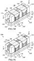
- a portion of the ILD structure 132 is removed to form contact openings 148 , as shown in FIGS. 1M and 2F in accordance with some embodiments.
- the ILD structure 132 and the CESL 131 are partially removed by an etching process, such as a dry etching process.
- an etching process such as a dry etching process.
- a portion of each of the S/D structures 130 is exposed by the contact openings 148 .
- the etching selectivity of the ILD structure 132 with respect to the mask layer 146 is high. Therefore, the etching process for forming the contact openings 148 is a self-aligned etching process. More specifically, the portion of the ILD structure 132 is removed by the etching process while the mask layer 146 is not removed. Since the remaining gate structures 140 ′′ are protected by the mask layer 146 , the remaining gate structures 140 ′′ are not damaged by the etchant during the etching process for forming the contact openings 148 .
- each of the air gaps 145 is the same as the second width W 2 of the second spacers 124 ′, and the air gaps 145 have a fifth height H 5 above the top surface of the fin structure 110 .
- an aspect ratio (H 5 /W 2 ) of each of the air gaps 145 is in a range from about 3 to about 6.
- the capacitances between the remaining gate structures 140 ′′ and the contacts 152 may not be reduced efficiently.
- the air gaps 145 may be filled up by the mask layer 146 easily, such that the capacitances between the remaining gate structures 140 ′′ and the contacts 152 may not be reduced efficiently as well.
- the second spacers 124 ′ are not entirely removed. For example, portions of the second spacers 124 ′ are left after the etching process of the second spacers 124 ′.
- the width of each of the air gaps 145 may be different from the second width W 2 of the second spacers 124 ′, and the width of each of the air gaps 145 may be in a range from about 1 nm to about 5 nm. For example, the width of each of the air gaps 145 may be about 3 nm.
- the fifth height H 5 of the air gaps 145 is greater than the third height H 3 of the remaining gate structures 140 ′.
- a difference between the fifth height H 5 and the third height H 3 is in a range from about 1 nm to about 5 nm.
- a difference between the fifth height H 5 and the third height H 3 is about 3 nm.
- the height of the first spacers 122 ′ is similar to the second height H 2 of the third spacers 126 ′.
- a ratio (H 2 /H 3 ) of the second height H 2 to the third height H 3 is in a range from about 2 to about 3.
- the remaining gate structures 140 ′′ may be too small, and high leakage current may occur.
- the ratio (H 2 /H 3 ) of the second height H 2 to the third height H 3 is too small, the remaining gate structures 140 ′′ may not be fully protected by the mask layer 146 during the self-aligned etching for forming the contact openings 148 in the subsequent processes.
- a barrier layer 150 is formed over the bottom surface and the sidewalls of each of the contact openings 148 , and a contact 152 is formed over each of the barrier layer 150 , as shown in FIGS. 1N and 2G in accordance with some embodiments.
- Each of the barrier layers 150 surrounds each of the contacts 152
- the ILD structure 132 surrounds the barrier layers 150 .
- the contacts 152 are electrically connected to the S/D structures 130 .
- the barrier layers 150 are made of tantalum (Ta), tantalum nitride (TaN), titanium (Ti), titanium nitride (TiN), cobalt tungsten (CoW) or another applicable material.
- the barrier layers 150 are made of Ti/TiN/W, and tungsten (W) in the barrier layers 150 has a smaller grain size than the grain size of the contacts 152 when the contacts 152 are made of tungsten (W).
- the barrier layers 150 are formed by a deposition process, such as a chemical vapor deposition (CVD) process, physical vapor deposition (PVD) process, atomic layer deposition (ALD) process, plating process or another application process.
- CVD chemical vapor deposition
- PVD physical vapor deposition
- ALD atomic layer deposition
- the contacts 152 are made of tungsten (W), cobalt (Co), titanium (Ti), aluminum (Al), copper (Cu), tantalum (Ta), platinum (Pt), molybdenum (Mo), silver (Ag), manganese (Mn), zirconium (Zr), ruthenium (Ru), or another application material.
- the contacts 152 are formed by a deposition process, such as a chemical vapor deposition (CVD) process, a physical vapor deposition (PVD) process, an atomic layer deposition (ALD) process, a plating process, or another application process.
- CVD chemical vapor deposition
- PVD physical vapor deposition
- ALD atomic layer deposition
- a glue layer may optionally be formed between each of the barrier layers 150 and each of the contacts 152 .
- the glue layers are used to improve adhesion between the barrier layers 150 and the contacts 152 . After the contacts 152 are formed, the FinFET device structure 100 a is obtained.
- the mask layer 146 is formed to cover the top surfaces of the remaining gate structures 140 ′′, and the fifth width W 5 of the mask layer 146 is greater than the fourth width W 4 of the remaining gate structures 140 ′′.
- the top surfaces of the first spacers 122 ′ are higher than the top surfaces of the remaining gate structures 140 ′′, and the top portions of the first spacers 122 ′ are embedded in the mask layer 146 .
- the remaining gate structures 140 ′′ will not be damaged by the etching etchant which is used for forming the contact openings 148 .
- the air gaps 145 which have a dielectric constant (about 1) lower than that of the first spacers 122 ′ and the third spacers 126 ′, are formed between the remaining gate structures 140 ′′ and the contacts 152 .
- the performance of the FinFET device structure 100 a may be increased.
- FIG. 3 is a cross-sectional representation of a modified FinFET device structure 100 b , in accordance with some embodiments of the disclosure.
- the FinFET device structure 100 b is similar to the FinFET device structure 100 a of FIG. 2G , and the difference between FIG. 3 and FIG. 2G is that the third spacers 126 ′ are not formed in FIG. 3 . Therefore, the air gaps 145 are sandwiched between the CESL 131 and the first spacers 122 ′.
- FIG. 4 is a cross-sectional representation of a modified FinFET device structure 100 c , in accordance with some embodiments of the disclosure.
- the FinFET device structure 100 c is similar to the FinFET device structure 100 a of FIG. 2G , and the difference between FIG. 4 and FIG. 2G is that the heights of the air gaps 145 in FIG. 4 are smaller than the heights of the air gaps 145 in FIG. 2G .
- the air gaps 145 in FIG. 4 have a sixth height H 6 above the top surface of the fin structure 110 , which is greater than the fifth height H 5 of the air gaps 145 in FIG. 2G . Therefore, the top surfaces of the remaining gate structures 140 ′′ are higher than the interfaces between the mask layer 146 and the air gaps 145 in FIG. 4 .
- FIG. 5 is a cross-sectional representation of a modified FinFET device structure 100 d , in accordance with some embodiments of the disclosure.
- the FinFET device structure 100 d is similar to the FinFET device structure 100 a of FIG. 2G , and the difference between FIG. 5 and FIG. 2G is that the second spacers 124 ′ are partially left after the etching process of the second spacers 124 ′ is performed.
- the fin structures 110 are covered by remaining portions 124 ′′ of the second spacers 124 ′, and the mask layer 146 is separated from the remaining portions 124 ′′ of the second spacers 124 ′ by the air gaps 145 .
- FIG. 6 is a cross-sectional representation of a modified FinFET device structure 100 e , in accordance with some embodiments of the disclosure.
- the FinFET device structure 100 e is similar to the FinFET device structure 100 a of FIG. 2G , and the difference between FIG. 6 and FIG. 2G is that some of the gaps 144 between the first spacers 122 ′ and the third spacers 126 ′ are entirely filled by the mask layer 146 .
- the mask layer 146 is separated from the fin structure 110 by one of the air gaps 145 at the left side of the left remaining gate structure 140 ′′, while the mask layer 146 is in direct contact with the fin structure 110 at the right side of the left remaining gate structure 140 ′′.
- FIG. 7 is a cross-sectional representation of a modified FinFET device structure 100 f , in accordance with some embodiments of the disclosure.
- the FinFET device structure 100 f is similar to the FinFET device structure 100 d of FIG. 5 , and the difference between FIG. 7 and FIG. 5 is that some of the gaps 144 between the first spacers 122 ′ and the third spacers 126 ′ are entirely filled by the mask layer 146 .
- the mask layer 146 is separated from the remaining portions 124 ′′ of the second spacers 124 ′ by one of the air gaps 145 at the left side of the left remaining gate structure 140 ′′, while the mask layer 146 is in direct contact with the remaining portions 124 ′′ of the second spacers 124 ′ at the right side of the left remaining gate structure 140 ′′.
- FIG. 8 is a cross-sectional representation of a modified FinFET device structure 100 g , in accordance with some embodiments of the disclosure.
- the FinFET device structure 100 g is similar to the FinFET device structure 100 a of FIG. 2G , and the difference between FIG. 8 and FIG. 2G is that the mask layer 146 is replaced with a first mask layer 146 ′ and a second mask layer 146 ′′ in FIG. 8 .
- the first mask layer 146 ′ is conformally formed covering the first spacers 122 ′, the third spacers 126 ′, the bottom surface and sidewalls of the gaps 144 between the first spacers 122 ′ and the third spacers 126 ′, and the sidewalls of the CESL 131 .
- the second mask layer 146 ′′ is formed over the first mask layer 146 ′. As a result, the air gaps 145 are enclosed by the first mask layer 146 ′ and the second mask layer 146 ′′.
- the first mask layer 146 ′ is made of silicon, nitride, silicon nitride or another applicable material.
- the first mask layer 146 is formed by a deposition process, such as an atomic layer deposition (ALD) process or another applicable process.
- ALD atomic layer deposition
- the second mask layer 146 ′′ is made of oxide, silicon oxide or another applicable material. In some embodiments, the second mask layer 146 ′′ is formed by a deposition process, such as a chemical vapor deposition (CVD) process or another applicable process.
- CVD chemical vapor deposition
- the first spacers 122 ′ are formed over the sidewalls of the remaining gate structures 140 ′′ and the second spacers 124 ′ are formed over the sidewalls of the first spacers 122 ′.
- the second spacers 124 ′ are removed by etching such that gaps 144 are formed between the first spacers 122 ′ and the contact etch stop layer (CESL) 131 adjacent to the remaining gate structures 140 ′′.
- the mask layer 146 is formed over the remaining gate structures 140 ′′ and the first spacers 122 ′.
- the mask layer 146 extends into upper portions of the gaps 144 such that lower portions of the gaps 144 forms air gaps 145 .
- the remaining gate structures 140 ′′ may be protected by the mask layer 146 during the subsequent processes. Moreover, the air gaps 145 covered by the mask layer 146 may be used to reduce the capacitance between the remaining gate structures 140 ′′ and the contacts 152 , which are electrically connected to the source/drain (S/D) structures 130 .
- S/D source/drain
- Embodiments of a FinFET device structure and method for forming the same are provided.
- the method for forming the FinFET device structure includes forming a first spacer and a second spacer over a sidewall of the gate structure, and forming a gap by etching the second spacer. After the gap is formed, a mask layer is formed covering the gate structure, the first spacer and the gap, such that an air gap is formed adjacent to the gate structure. Since the dielectric constant of the air gap is lower than that of the first spacer, the capacitance between the gate structure and the adjacent contact may be reduced, and the performance of the FinFET device structure may be increased.
- a method for forming a FinFET device structure includes forming a fin structure over a substrate and forming a gate structure across the fin structure.
- the method for forming a FinFET device structure also includes forming a first spacer over a sidewall of the gate structure and forming a second spacer over the first spacer.
- the method for forming a FinFET device structure further includes etching the second spacer to form a gap and forming a mask layer over the gate structure and the first spacer after the gap is formed.
- the mask layer extends into the gap such that the mask layer and the fin structure are separated by an air gap in the gap.
- a method for forming a FinFET device structure includes forming a fin structure over a substrate and forming a gate structure across the fin structure.
- the method for forming a FinFET device structure also includes forming a first spacer over a sidewall of the gate structure and forming a second spacer over a sidewall of the first spacer.
- the method for forming a FinFET device structure further includes removing a first portion of the gate structure to form a first opening and partially removing the first spacer and the second spacer through the first opening.
- the method for forming a FinFET device structure includes removing a second portion of the gate structure to form a second opening below the first opening and etching the second spacer to form a gap after the second opening is formed.
- the method for forming a FinFET device structure also includes forming a mask layer covering the gate structure, the first spacer and the gap such that an air gap is formed in the gap.
- a FinFET device structure in some embodiments, includes a fin structure formed over a substrate and a gate structure formed over the fin structure.
- the FinFET device structure also includes a first spacer formed on a sidewall of the gate structure and a contact formed over the fin structure and adjacent to the gate structure. The contact and the first spacer have an air gap therebetween.
- the FinFET device structure further includes a mask layer formed over the gate structure, the first spacer and the air gap. The top surface of the first spacer is higher than the interface between the mask layer and the air gap.
Landscapes
- Engineering & Computer Science (AREA)
- Manufacturing & Machinery (AREA)
- Physics & Mathematics (AREA)
- Condensed Matter Physics & Semiconductors (AREA)
- General Physics & Mathematics (AREA)
- Computer Hardware Design (AREA)
- Microelectronics & Electronic Packaging (AREA)
- Power Engineering (AREA)
- Inorganic Chemistry (AREA)
- Chemical & Material Sciences (AREA)
- Insulated Gate Type Field-Effect Transistor (AREA)
- Thin Film Transistor (AREA)
- Internal Circuitry In Semiconductor Integrated Circuit Devices (AREA)
Abstract
Description
Claims (20)
Priority Applications (1)
| Application Number | Priority Date | Filing Date | Title |
|---|---|---|---|
| US16/135,108 US11101385B2 (en) | 2018-09-19 | 2018-09-19 | Fin field effect transistor (FinFET) device structure with air gap and method for forming the same |
Applications Claiming Priority (1)
| Application Number | Priority Date | Filing Date | Title |
|---|---|---|---|
| US16/135,108 US11101385B2 (en) | 2018-09-19 | 2018-09-19 | Fin field effect transistor (FinFET) device structure with air gap and method for forming the same |
Publications (2)
| Publication Number | Publication Date |
|---|---|
| US20200091345A1 US20200091345A1 (en) | 2020-03-19 |
| US11101385B2 true US11101385B2 (en) | 2021-08-24 |
Family
ID=69773380
Family Applications (1)
| Application Number | Title | Priority Date | Filing Date |
|---|---|---|---|
| US16/135,108 Active 2038-10-06 US11101385B2 (en) | 2018-09-19 | 2018-09-19 | Fin field effect transistor (FinFET) device structure with air gap and method for forming the same |
Country Status (1)
| Country | Link |
|---|---|
| US (1) | US11101385B2 (en) |
Families Citing this family (13)
| Publication number | Priority date | Publication date | Assignee | Title |
|---|---|---|---|---|
| US11527444B2 (en) * | 2019-09-25 | 2022-12-13 | Taiwan Semiconductor Manufacturing Co., Ltd. | Air spacer formation for semiconductor devices |
| KR102737495B1 (en) * | 2020-01-10 | 2024-12-04 | 삼성전자주식회사 | Semiconductor device including self-aligned contact and manufacturing method thereof |
| US11217679B2 (en) | 2020-04-01 | 2022-01-04 | Taiwan Semiconductor Manufacturing Company, Ltd. | Semiconductor device and method |
| US11817491B2 (en) * | 2020-07-21 | 2023-11-14 | Taiwan Semiconductor Manufacturing Co., Ltd. | Semiconductor device having an air gap along a gate spacer |
| KR20220107847A (en) | 2021-01-26 | 2022-08-02 | 삼성전자주식회사 | Integrated circuit device and method of manufacturing the same |
| US12125886B2 (en) * | 2021-03-10 | 2024-10-22 | Taiwan Semiconductor Manufacturing Co., Ltd. | Fin field-effect transistor device and method |
| KR102901410B1 (en) | 2021-03-15 | 2025-12-18 | 삼성전자주식회사 | Semiconductor device |
| US11837631B2 (en) * | 2021-04-09 | 2023-12-05 | Taiwan Semiconductor Manufacturing Company, Ltd. | Source/drain spacer with air gap in semiconductor devices and methods of fabricating the same |
| US11769770B2 (en) * | 2021-05-06 | 2023-09-26 | Taiwan Semiconductor Manufacturing Company, Ltd. | Methods of forming a semiconductor device having an air spacer |
| KR20220158340A (en) * | 2021-05-24 | 2022-12-01 | 삼성전자주식회사 | Semiconductor devices including gate structure and method of forming the same |
| KR102845403B1 (en) | 2021-07-21 | 2025-08-13 | 삼성전자주식회사 | Semiconductor device and method for manufacturing the same |
| US12107146B2 (en) * | 2021-08-05 | 2024-10-01 | Taiwan Semiconductor Manufacturing Company, Ltd. | Self-aligned air spacers and methods for forming |
| US20230230876A1 (en) * | 2022-01-18 | 2023-07-20 | Taiwan Semiconductor Manufacturing Company, Ltd. | Method of forming a cap layer for sealing an air gap, and semiconductor device |
Citations (18)
| Publication number | Priority date | Publication date | Assignee | Title |
|---|---|---|---|---|
| US20130248950A1 (en) * | 2012-03-20 | 2013-09-26 | Samsung Electronics Co., Ltd. | Semiconductor devices and method of manufacturing the same |
| US8772109B2 (en) | 2012-10-24 | 2014-07-08 | Taiwan Semiconductor Manufacturing Company, Ltd. | Apparatus and method for forming semiconductor contacts |
| US8785285B2 (en) | 2012-03-08 | 2014-07-22 | Taiwan Semiconductor Manufacturing Company, Ltd. | Semiconductor devices and methods of manufacture thereof |
| US8816444B2 (en) | 2011-04-29 | 2014-08-26 | Taiwan Semiconductor Manufacturing Company, Ltd. | System and methods for converting planar design to FinFET design |
| US8823065B2 (en) | 2012-11-08 | 2014-09-02 | Taiwan Semiconductor Manufacturing Company, Ltd. | Contact structure of semiconductor device |
| US20140264480A1 (en) * | 2013-03-14 | 2014-09-18 | United Microelectronics Corp. | Semiconductor device and method of forming the same |
| US8860148B2 (en) | 2012-04-11 | 2014-10-14 | Taiwan Semiconductor Manufacturing Company, Ltd. | Structure and method for FinFET integrated with capacitor |
| US9105490B2 (en) | 2012-09-27 | 2015-08-11 | Taiwan Semiconductor Manufacturing Company, Ltd. | Contact structure of semiconductor device |
| US9236267B2 (en) | 2012-02-09 | 2016-01-12 | Taiwan Semiconductor Manufacturing Company, Ltd. | Cut-mask patterning process for fin-like field effect transistor (FinFET) device |
| US9236300B2 (en) | 2012-11-30 | 2016-01-12 | Taiwan Semiconductor Manufacturing Company, Ltd. | Contact plugs in SRAM cells and the method of forming the same |
| US9520482B1 (en) | 2015-11-13 | 2016-12-13 | Taiwan Semiconductor Manufacturing Company, Ltd. | Method of cutting metal gate |
| US9536982B1 (en) * | 2015-11-03 | 2017-01-03 | International Business Machines Corporation | Etch stop for airgap protection |
| US9576814B2 (en) | 2013-12-19 | 2017-02-21 | Taiwan Semiconductor Manufacturing Company, Ltd. | Method of spacer patterning to form a target integrated circuit pattern |
| US20170179241A1 (en) * | 2015-12-18 | 2017-06-22 | Taiwan Semiconductor Manufacturing Co., Ltd. | Semiconductor structure and manufacturing method thereof |
| US20180090593A1 (en) * | 2016-09-27 | 2018-03-29 | International Business Machines Corporation | Transistor with air spacer and self-aligned contact |
| US10008578B1 (en) * | 2017-06-06 | 2018-06-26 | United Microelectronics Corp. | Semiconductor device and method for fabricating the same |
| US20190172752A1 (en) * | 2017-12-04 | 2019-06-06 | United Microelectronics Corp. | Semiconductor device and method for fabricating the same |
| US20190393335A1 (en) * | 2018-06-25 | 2019-12-26 | Globalfoundries Inc. | Method for forming replacement air gap |
-
2018
- 2018-09-19 US US16/135,108 patent/US11101385B2/en active Active
Patent Citations (18)
| Publication number | Priority date | Publication date | Assignee | Title |
|---|---|---|---|---|
| US8816444B2 (en) | 2011-04-29 | 2014-08-26 | Taiwan Semiconductor Manufacturing Company, Ltd. | System and methods for converting planar design to FinFET design |
| US9236267B2 (en) | 2012-02-09 | 2016-01-12 | Taiwan Semiconductor Manufacturing Company, Ltd. | Cut-mask patterning process for fin-like field effect transistor (FinFET) device |
| US8785285B2 (en) | 2012-03-08 | 2014-07-22 | Taiwan Semiconductor Manufacturing Company, Ltd. | Semiconductor devices and methods of manufacture thereof |
| US20130248950A1 (en) * | 2012-03-20 | 2013-09-26 | Samsung Electronics Co., Ltd. | Semiconductor devices and method of manufacturing the same |
| US8860148B2 (en) | 2012-04-11 | 2014-10-14 | Taiwan Semiconductor Manufacturing Company, Ltd. | Structure and method for FinFET integrated with capacitor |
| US9105490B2 (en) | 2012-09-27 | 2015-08-11 | Taiwan Semiconductor Manufacturing Company, Ltd. | Contact structure of semiconductor device |
| US8772109B2 (en) | 2012-10-24 | 2014-07-08 | Taiwan Semiconductor Manufacturing Company, Ltd. | Apparatus and method for forming semiconductor contacts |
| US8823065B2 (en) | 2012-11-08 | 2014-09-02 | Taiwan Semiconductor Manufacturing Company, Ltd. | Contact structure of semiconductor device |
| US9236300B2 (en) | 2012-11-30 | 2016-01-12 | Taiwan Semiconductor Manufacturing Company, Ltd. | Contact plugs in SRAM cells and the method of forming the same |
| US20140264480A1 (en) * | 2013-03-14 | 2014-09-18 | United Microelectronics Corp. | Semiconductor device and method of forming the same |
| US9576814B2 (en) | 2013-12-19 | 2017-02-21 | Taiwan Semiconductor Manufacturing Company, Ltd. | Method of spacer patterning to form a target integrated circuit pattern |
| US9536982B1 (en) * | 2015-11-03 | 2017-01-03 | International Business Machines Corporation | Etch stop for airgap protection |
| US9520482B1 (en) | 2015-11-13 | 2016-12-13 | Taiwan Semiconductor Manufacturing Company, Ltd. | Method of cutting metal gate |
| US20170179241A1 (en) * | 2015-12-18 | 2017-06-22 | Taiwan Semiconductor Manufacturing Co., Ltd. | Semiconductor structure and manufacturing method thereof |
| US20180090593A1 (en) * | 2016-09-27 | 2018-03-29 | International Business Machines Corporation | Transistor with air spacer and self-aligned contact |
| US10008578B1 (en) * | 2017-06-06 | 2018-06-26 | United Microelectronics Corp. | Semiconductor device and method for fabricating the same |
| US20190172752A1 (en) * | 2017-12-04 | 2019-06-06 | United Microelectronics Corp. | Semiconductor device and method for fabricating the same |
| US20190393335A1 (en) * | 2018-06-25 | 2019-12-26 | Globalfoundries Inc. | Method for forming replacement air gap |
Also Published As
| Publication number | Publication date |
|---|---|
| US20200091345A1 (en) | 2020-03-19 |
Similar Documents
| Publication | Publication Date | Title |
|---|---|---|
| US11101385B2 (en) | Fin field effect transistor (FinFET) device structure with air gap and method for forming the same | |
| US11594634B2 (en) | Fin field effect transistor (FinFET) device structure with stop layer and method for forming the same | |
| US11139295B2 (en) | Fin field effect transistor (FinFET) device and method | |
| US11011636B2 (en) | Fin field effect transistor (FinFET) device structure with hard mask layer over gate structure and method for forming the same | |
| US10868184B2 (en) | Fin field effect transistor (FinFET) device structure with hard mask layer over gate structure and method for forming the same | |
| US11158512B2 (en) | Fin field effect transistor (FinFET) device structure | |
| US12176435B2 (en) | Method for forming fin field effect transistor (FinFET) device structure with conductive layer between gate and gate contact | |
| US12107166B2 (en) | Fin field effect transistor (FinFET) device structure with isolation layer and method for forming the same | |
| US11088250B2 (en) | Fin field effect transistor (FinFET) device structure with dual spacers and method for forming the same | |
| US20250359137A1 (en) | Disposable Hard Mask for Interconnect Formation | |
| US11626504B2 (en) | Fin field effect transistor (FinFET) device structure | |
| US11777004B2 (en) | Fin field effect transistor (FinFET) device structure and method for forming the same | |
| US11563110B2 (en) | Semiconductor structure and method for forming the same | |
| US12402345B2 (en) | Semiconductor structure and method for forming the same | |
| US20240030138A1 (en) | Semiconductor device structure and method for forming the same | |
| US20220399461A1 (en) | Semiconductor device structure and method for forming the same |
Legal Events
| Date | Code | Title | Description |
|---|---|---|---|
| FEPP | Fee payment procedure |
Free format text: ENTITY STATUS SET TO UNDISCOUNTED (ORIGINAL EVENT CODE: BIG.); ENTITY STATUS OF PATENT OWNER: LARGE ENTITY |
|
| AS | Assignment |
Owner name: TAIWAN SEMICONDUCTOR MANUFACTURING CO., LTD., TAIWAN Free format text: ASSIGNMENT OF ASSIGNORS INTEREST;ASSIGNORS:CHIU, WEN-LI;CHIANG, HSIN-CHE;LIANG, CHUN-SHENG;AND OTHERS;REEL/FRAME:047296/0262 Effective date: 20181005 |
|
| STPP | Information on status: patent application and granting procedure in general |
Free format text: NON FINAL ACTION MAILED |
|
| STPP | Information on status: patent application and granting procedure in general |
Free format text: RESPONSE AFTER FINAL ACTION FORWARDED TO EXAMINER |
|
| STPP | Information on status: patent application and granting procedure in general |
Free format text: DOCKETED NEW CASE - READY FOR EXAMINATION |
|
| STPP | Information on status: patent application and granting procedure in general |
Free format text: NOTICE OF ALLOWANCE MAILED -- APPLICATION RECEIVED IN OFFICE OF PUBLICATIONS |
|
| STCF | Information on status: patent grant |
Free format text: PATENTED CASE |
|
| MAFP | Maintenance fee payment |
Free format text: PAYMENT OF MAINTENANCE FEE, 4TH YEAR, LARGE ENTITY (ORIGINAL EVENT CODE: M1551); ENTITY STATUS OF PATENT OWNER: LARGE ENTITY Year of fee payment: 4 |