US11100859B2 - Processing circuit, display device, and processing method for reducing current during luminance change - Google Patents
Processing circuit, display device, and processing method for reducing current during luminance change Download PDFInfo
- Publication number
- US11100859B2 US11100859B2 US16/774,743 US202016774743A US11100859B2 US 11100859 B2 US11100859 B2 US 11100859B2 US 202016774743 A US202016774743 A US 202016774743A US 11100859 B2 US11100859 B2 US 11100859B2
- Authority
- US
- United States
- Prior art keywords
- video signal
- current
- luminance
- processing circuit
- pixels
- Prior art date
- Legal status (The legal status is an assumption and is not a legal conclusion. Google has not performed a legal analysis and makes no representation as to the accuracy of the status listed.)
- Active
Links
Images


Classifications
-
- G—PHYSICS
- G09—EDUCATION; CRYPTOGRAPHY; DISPLAY; ADVERTISING; SEALS
- G09G—ARRANGEMENTS OR CIRCUITS FOR CONTROL OF INDICATING DEVICES USING STATIC MEANS TO PRESENT VARIABLE INFORMATION
- G09G3/00—Control arrangements or circuits, of interest only in connection with visual indicators other than cathode-ray tubes
- G09G3/20—Control arrangements or circuits, of interest only in connection with visual indicators other than cathode-ray tubes for presentation of an assembly of a number of characters, e.g. a page, by composing the assembly by combination of individual elements arranged in a matrix no fixed position being assigned to or needed to be assigned to the individual characters or partial characters
- G09G3/22—Control arrangements or circuits, of interest only in connection with visual indicators other than cathode-ray tubes for presentation of an assembly of a number of characters, e.g. a page, by composing the assembly by combination of individual elements arranged in a matrix no fixed position being assigned to or needed to be assigned to the individual characters or partial characters using controlled light sources
- G09G3/30—Control arrangements or circuits, of interest only in connection with visual indicators other than cathode-ray tubes for presentation of an assembly of a number of characters, e.g. a page, by composing the assembly by combination of individual elements arranged in a matrix no fixed position being assigned to or needed to be assigned to the individual characters or partial characters using controlled light sources using electroluminescent panels
- G09G3/32—Control arrangements or circuits, of interest only in connection with visual indicators other than cathode-ray tubes for presentation of an assembly of a number of characters, e.g. a page, by composing the assembly by combination of individual elements arranged in a matrix no fixed position being assigned to or needed to be assigned to the individual characters or partial characters using controlled light sources using electroluminescent panels semiconductive, e.g. using light-emitting diodes [LED]
- G09G3/3208—Control arrangements or circuits, of interest only in connection with visual indicators other than cathode-ray tubes for presentation of an assembly of a number of characters, e.g. a page, by composing the assembly by combination of individual elements arranged in a matrix no fixed position being assigned to or needed to be assigned to the individual characters or partial characters using controlled light sources using electroluminescent panels semiconductive, e.g. using light-emitting diodes [LED] organic, e.g. using organic light-emitting diodes [OLED]
- G09G3/3225—Control arrangements or circuits, of interest only in connection with visual indicators other than cathode-ray tubes for presentation of an assembly of a number of characters, e.g. a page, by composing the assembly by combination of individual elements arranged in a matrix no fixed position being assigned to or needed to be assigned to the individual characters or partial characters using controlled light sources using electroluminescent panels semiconductive, e.g. using light-emitting diodes [LED] organic, e.g. using organic light-emitting diodes [OLED] using an active matrix
- G09G3/3233—Control arrangements or circuits, of interest only in connection with visual indicators other than cathode-ray tubes for presentation of an assembly of a number of characters, e.g. a page, by composing the assembly by combination of individual elements arranged in a matrix no fixed position being assigned to or needed to be assigned to the individual characters or partial characters using controlled light sources using electroluminescent panels semiconductive, e.g. using light-emitting diodes [LED] organic, e.g. using organic light-emitting diodes [OLED] using an active matrix with pixel circuitry controlling the current through the light-emitting element
-
- G—PHYSICS
- G09—EDUCATION; CRYPTOGRAPHY; DISPLAY; ADVERTISING; SEALS
- G09G—ARRANGEMENTS OR CIRCUITS FOR CONTROL OF INDICATING DEVICES USING STATIC MEANS TO PRESENT VARIABLE INFORMATION
- G09G3/00—Control arrangements or circuits, of interest only in connection with visual indicators other than cathode-ray tubes
- G09G3/20—Control arrangements or circuits, of interest only in connection with visual indicators other than cathode-ray tubes for presentation of an assembly of a number of characters, e.g. a page, by composing the assembly by combination of individual elements arranged in a matrix no fixed position being assigned to or needed to be assigned to the individual characters or partial characters
- G09G3/22—Control arrangements or circuits, of interest only in connection with visual indicators other than cathode-ray tubes for presentation of an assembly of a number of characters, e.g. a page, by composing the assembly by combination of individual elements arranged in a matrix no fixed position being assigned to or needed to be assigned to the individual characters or partial characters using controlled light sources
- G09G3/30—Control arrangements or circuits, of interest only in connection with visual indicators other than cathode-ray tubes for presentation of an assembly of a number of characters, e.g. a page, by composing the assembly by combination of individual elements arranged in a matrix no fixed position being assigned to or needed to be assigned to the individual characters or partial characters using controlled light sources using electroluminescent panels
- G09G3/32—Control arrangements or circuits, of interest only in connection with visual indicators other than cathode-ray tubes for presentation of an assembly of a number of characters, e.g. a page, by composing the assembly by combination of individual elements arranged in a matrix no fixed position being assigned to or needed to be assigned to the individual characters or partial characters using controlled light sources using electroluminescent panels semiconductive, e.g. using light-emitting diodes [LED]
- G09G3/3208—Control arrangements or circuits, of interest only in connection with visual indicators other than cathode-ray tubes for presentation of an assembly of a number of characters, e.g. a page, by composing the assembly by combination of individual elements arranged in a matrix no fixed position being assigned to or needed to be assigned to the individual characters or partial characters using controlled light sources using electroluminescent panels semiconductive, e.g. using light-emitting diodes [LED] organic, e.g. using organic light-emitting diodes [OLED]
- G09G3/3225—Control arrangements or circuits, of interest only in connection with visual indicators other than cathode-ray tubes for presentation of an assembly of a number of characters, e.g. a page, by composing the assembly by combination of individual elements arranged in a matrix no fixed position being assigned to or needed to be assigned to the individual characters or partial characters using controlled light sources using electroluminescent panels semiconductive, e.g. using light-emitting diodes [LED] organic, e.g. using organic light-emitting diodes [OLED] using an active matrix
-
- G—PHYSICS
- G09—EDUCATION; CRYPTOGRAPHY; DISPLAY; ADVERTISING; SEALS
- G09G—ARRANGEMENTS OR CIRCUITS FOR CONTROL OF INDICATING DEVICES USING STATIC MEANS TO PRESENT VARIABLE INFORMATION
- G09G3/00—Control arrangements or circuits, of interest only in connection with visual indicators other than cathode-ray tubes
- G09G3/20—Control arrangements or circuits, of interest only in connection with visual indicators other than cathode-ray tubes for presentation of an assembly of a number of characters, e.g. a page, by composing the assembly by combination of individual elements arranged in a matrix no fixed position being assigned to or needed to be assigned to the individual characters or partial characters
- G09G3/2085—Special arrangements for addressing the individual elements of the matrix, other than by driving respective rows and columns in combination
-
- G—PHYSICS
- G09—EDUCATION; CRYPTOGRAPHY; DISPLAY; ADVERTISING; SEALS
- G09G—ARRANGEMENTS OR CIRCUITS FOR CONTROL OF INDICATING DEVICES USING STATIC MEANS TO PRESENT VARIABLE INFORMATION
- G09G3/00—Control arrangements or circuits, of interest only in connection with visual indicators other than cathode-ray tubes
- G09G3/20—Control arrangements or circuits, of interest only in connection with visual indicators other than cathode-ray tubes for presentation of an assembly of a number of characters, e.g. a page, by composing the assembly by combination of individual elements arranged in a matrix no fixed position being assigned to or needed to be assigned to the individual characters or partial characters
- G09G3/22—Control arrangements or circuits, of interest only in connection with visual indicators other than cathode-ray tubes for presentation of an assembly of a number of characters, e.g. a page, by composing the assembly by combination of individual elements arranged in a matrix no fixed position being assigned to or needed to be assigned to the individual characters or partial characters using controlled light sources
- G09G3/30—Control arrangements or circuits, of interest only in connection with visual indicators other than cathode-ray tubes for presentation of an assembly of a number of characters, e.g. a page, by composing the assembly by combination of individual elements arranged in a matrix no fixed position being assigned to or needed to be assigned to the individual characters or partial characters using controlled light sources using electroluminescent panels
- G09G3/32—Control arrangements or circuits, of interest only in connection with visual indicators other than cathode-ray tubes for presentation of an assembly of a number of characters, e.g. a page, by composing the assembly by combination of individual elements arranged in a matrix no fixed position being assigned to or needed to be assigned to the individual characters or partial characters using controlled light sources using electroluminescent panels semiconductive, e.g. using light-emitting diodes [LED]
- G09G3/3208—Control arrangements or circuits, of interest only in connection with visual indicators other than cathode-ray tubes for presentation of an assembly of a number of characters, e.g. a page, by composing the assembly by combination of individual elements arranged in a matrix no fixed position being assigned to or needed to be assigned to the individual characters or partial characters using controlled light sources using electroluminescent panels semiconductive, e.g. using light-emitting diodes [LED] organic, e.g. using organic light-emitting diodes [OLED]
- G09G3/3275—Details of drivers for data electrodes
- G09G3/3291—Details of drivers for data electrodes in which the data driver supplies a variable data voltage for setting the current through, or the voltage across, the light-emitting elements
-
- G—PHYSICS
- G09—EDUCATION; CRYPTOGRAPHY; DISPLAY; ADVERTISING; SEALS
- G09G—ARRANGEMENTS OR CIRCUITS FOR CONTROL OF INDICATING DEVICES USING STATIC MEANS TO PRESENT VARIABLE INFORMATION
- G09G5/00—Control arrangements or circuits for visual indicators common to cathode-ray tube indicators and other visual indicators
- G09G5/003—Details of a display terminal, the details relating to the control arrangement of the display terminal and to the interfaces thereto
- G09G5/006—Details of the interface to the display terminal
- G09G5/008—Clock recovery
-
- H—ELECTRICITY
- H04—ELECTRIC COMMUNICATION TECHNIQUE
- H04N—PICTORIAL COMMUNICATION, e.g. TELEVISION
- H04N25/00—Circuitry of solid-state image sensors [SSIS]; Control thereof
- H04N25/70—SSIS architectures; Circuits associated therewith
- H04N25/703—SSIS architectures incorporating pixels for producing signals other than image signals
- H04N25/705—Pixels for depth measurement, e.g. RGBZ
-
- H04N5/36965—
-
- G—PHYSICS
- G09—EDUCATION; CRYPTOGRAPHY; DISPLAY; ADVERTISING; SEALS
- G09G—ARRANGEMENTS OR CIRCUITS FOR CONTROL OF INDICATING DEVICES USING STATIC MEANS TO PRESENT VARIABLE INFORMATION
- G09G2300/00—Aspects of the constitution of display devices
- G09G2300/08—Active matrix structure, i.e. with use of active elements, inclusive of non-linear two terminal elements, in the pixels together with light emitting or modulating elements
- G09G2300/0809—Several active elements per pixel in active matrix panels
- G09G2300/0842—Several active elements per pixel in active matrix panels forming a memory circuit, e.g. a dynamic memory with one capacitor
-
- G—PHYSICS
- G09—EDUCATION; CRYPTOGRAPHY; DISPLAY; ADVERTISING; SEALS
- G09G—ARRANGEMENTS OR CIRCUITS FOR CONTROL OF INDICATING DEVICES USING STATIC MEANS TO PRESENT VARIABLE INFORMATION
- G09G2310/00—Command of the display device
- G09G2310/02—Addressing, scanning or driving the display screen or processing steps related thereto
- G09G2310/0202—Addressing of scan or signal lines
- G09G2310/0213—Addressing of scan or signal lines controlling the sequence of the scanning lines with respect to the patterns to be displayed, e.g. to save power
-
- G—PHYSICS
- G09—EDUCATION; CRYPTOGRAPHY; DISPLAY; ADVERTISING; SEALS
- G09G—ARRANGEMENTS OR CIRCUITS FOR CONTROL OF INDICATING DEVICES USING STATIC MEANS TO PRESENT VARIABLE INFORMATION
- G09G2320/00—Control of display operating conditions
- G09G2320/02—Improving the quality of display appearance
- G09G2320/0233—Improving the luminance or brightness uniformity across the screen
-
- G—PHYSICS
- G09—EDUCATION; CRYPTOGRAPHY; DISPLAY; ADVERTISING; SEALS
- G09G—ARRANGEMENTS OR CIRCUITS FOR CONTROL OF INDICATING DEVICES USING STATIC MEANS TO PRESENT VARIABLE INFORMATION
- G09G2320/00—Control of display operating conditions
- G09G2320/02—Improving the quality of display appearance
- G09G2320/0271—Adjustment of the gradation levels within the range of the gradation scale, e.g. by redistribution or clipping
-
- G—PHYSICS
- G09—EDUCATION; CRYPTOGRAPHY; DISPLAY; ADVERTISING; SEALS
- G09G—ARRANGEMENTS OR CIRCUITS FOR CONTROL OF INDICATING DEVICES USING STATIC MEANS TO PRESENT VARIABLE INFORMATION
- G09G2320/00—Control of display operating conditions
- G09G2320/02—Improving the quality of display appearance
- G09G2320/029—Improving the quality of display appearance by monitoring one or more pixels in the display panel, e.g. by monitoring a fixed reference pixel
- G09G2320/0295—Improving the quality of display appearance by monitoring one or more pixels in the display panel, e.g. by monitoring a fixed reference pixel by monitoring each display pixel
-
- G—PHYSICS
- G09—EDUCATION; CRYPTOGRAPHY; DISPLAY; ADVERTISING; SEALS
- G09G—ARRANGEMENTS OR CIRCUITS FOR CONTROL OF INDICATING DEVICES USING STATIC MEANS TO PRESENT VARIABLE INFORMATION
- G09G2320/00—Control of display operating conditions
- G09G2320/04—Maintaining the quality of display appearance
- G09G2320/043—Preventing or counteracting the effects of ageing
-
- G—PHYSICS
- G09—EDUCATION; CRYPTOGRAPHY; DISPLAY; ADVERTISING; SEALS
- G09G—ARRANGEMENTS OR CIRCUITS FOR CONTROL OF INDICATING DEVICES USING STATIC MEANS TO PRESENT VARIABLE INFORMATION
- G09G2320/00—Control of display operating conditions
- G09G2320/06—Adjustment of display parameters
- G09G2320/0626—Adjustment of display parameters for control of overall brightness
- G09G2320/0633—Adjustment of display parameters for control of overall brightness by amplitude modulation of the brightness of the illumination source
-
- G—PHYSICS
- G09—EDUCATION; CRYPTOGRAPHY; DISPLAY; ADVERTISING; SEALS
- G09G—ARRANGEMENTS OR CIRCUITS FOR CONTROL OF INDICATING DEVICES USING STATIC MEANS TO PRESENT VARIABLE INFORMATION
- G09G2330/00—Aspects of power supply; Aspects of display protection and defect management
- G09G2330/02—Details of power systems and of start or stop of display operation
- G09G2330/021—Power management, e.g. power saving
-
- G—PHYSICS
- G09—EDUCATION; CRYPTOGRAPHY; DISPLAY; ADVERTISING; SEALS
- G09G—ARRANGEMENTS OR CIRCUITS FOR CONTROL OF INDICATING DEVICES USING STATIC MEANS TO PRESENT VARIABLE INFORMATION
- G09G2360/00—Aspects of the architecture of display systems
- G09G2360/08—Power processing, i.e. workload management for processors involved in display operations, such as CPUs or GPUs
-
- G—PHYSICS
- G09—EDUCATION; CRYPTOGRAPHY; DISPLAY; ADVERTISING; SEALS
- G09G—ARRANGEMENTS OR CIRCUITS FOR CONTROL OF INDICATING DEVICES USING STATIC MEANS TO PRESENT VARIABLE INFORMATION
- G09G2360/00—Aspects of the architecture of display systems
- G09G2360/16—Calculation or use of calculated indices related to luminance levels in display data
-
- G—PHYSICS
- G09—EDUCATION; CRYPTOGRAPHY; DISPLAY; ADVERTISING; SEALS
- G09G—ARRANGEMENTS OR CIRCUITS FOR CONTROL OF INDICATING DEVICES USING STATIC MEANS TO PRESENT VARIABLE INFORMATION
- G09G2360/00—Aspects of the architecture of display systems
- G09G2360/18—Use of a frame buffer in a display terminal, inclusive of the display panel
-
- G—PHYSICS
- G09—EDUCATION; CRYPTOGRAPHY; DISPLAY; ADVERTISING; SEALS
- G09G—ARRANGEMENTS OR CIRCUITS FOR CONTROL OF INDICATING DEVICES USING STATIC MEANS TO PRESENT VARIABLE INFORMATION
- G09G2370/00—Aspects of data communication
- G09G2370/08—Details of image data interface between the display device controller and the data line driver circuit
-
- G—PHYSICS
- G09—EDUCATION; CRYPTOGRAPHY; DISPLAY; ADVERTISING; SEALS
- G09G—ARRANGEMENTS OR CIRCUITS FOR CONTROL OF INDICATING DEVICES USING STATIC MEANS TO PRESENT VARIABLE INFORMATION
- G09G5/00—Control arrangements or circuits for visual indicators common to cathode-ray tube indicators and other visual indicators
- G09G5/36—Control arrangements or circuits for visual indicators common to cathode-ray tube indicators and other visual indicators characterised by the display of a graphic pattern, e.g. using an all-points-addressable [APA] memory
- G09G5/39—Control of the bit-mapped memory
- G09G5/395—Arrangements specially adapted for transferring the contents of the bit-mapped memory to the screen
Definitions
- the present disclosure relates to a processing circuit, a display device, and a processing method.
- display devices each including pixels each having a self light emitting element have been developed.
- the display devices include organic electro-luminescent (EL) display devices.
- EL organic electro-luminescent
- increase in the size of a display panel has been desired.
- the increase in the size of the display panel is accompanied by increase in electric power to be consumed in the display device.
- a technique for reducing electric power consumption in a display device has been known (see Patent Literature 1).
- the electric power consumption in the display panel is reduced by calculating electric power consumption in the display panel for each horizontal period (horizontal synchronization period) based on a video signal, and limiting a current to be supplied to each of pixels of the display panel, based on the result of the calculation.
- the display device disclosed in Patent Literature 1 tries to reduce the electric power consumption in the display panel to a control target electric power value or below.
- Patent Literature 1 Japanese Unexamined Patent Application Publication No. 2007-212644
- Patent Literature 1 when a luminance represented by a video signal abruptly increases as, for example, in the case of switching from all black display to all white display, the electric power consumption of the display panel may exceed the control target electric power value.
- the present disclosure has been made considering the above problem, and has an object to provide a processing circuit, etc., capable of reducing a current to be supplied to the display panel even when the luminance represented by a video signal abruptly increases.
- a processing circuit which processes video signals for a display device which includes a display panel and a current limiting circuit.
- the display panel includes a plurality of pixels each having a self light emitting element, and the current limiting circuit limits a current to be supplied to the plurality of pixels.
- the processing circuit includes a frame memory which stores video signals of a previous frame which is a frame before a current frame to be input to the processing circuit. The video signals correspond to the plurality of pixels.
- the processing circuit also includes a signal processer which: compares a luminance represented by a video signal which is included in video signals of the current frame and which corresponds to a pixel included in the plurality of pixels and a luminance represented by a video signal which is included in the video signals of the previous frame and which corresponds to the pixel; outputs the video signal of the current frame as it is in a case where the luminance represented by the video signal of the current frame is equal to or smaller than the luminance represented by the video signal of the previous frame or equal to or smaller than a predetermined threshold value; and outputs a weighted average of the video signal of the current frame and the video signal of the previous frame in any other case.
- a signal processer which: compares a luminance represented by a video signal which is included in video signals of the current frame and which corresponds to a pixel included in the plurality of pixels and a luminance represented by a video signal which is included in the video signals of the previous frame and which corresponds to the pixel; outputs the video signal
- a display device includes the processing circuit, the display panel, and the current limiting circuit.
- a processing method for processing video signals for a display device which includes a display panel and a current limiting circuit.
- the display panel includes a plurality of pixels each having a self light emitting element, and the current limiting circuit limiting a current to be supplied to the plurality of pixels.
- the processing method includes a step of storing video signals of a previous frame which is a frame before a current frame, the video signals corresponding to the plurality of pixels.
- the processing method also includes a step including: comparing a luminance represented by a video signal which is included in video signals of the current frame and which corresponds to a pixel included in the plurality of pixels and a luminance represented by a video signal which is included in the video signals of the previous frame and which corresponds to the pixel; outputting the video signal of the current frame as it is in a case where the luminance represented by the video signal of the current frame is equal to or smaller than the luminance represented by the video signal of the previous frame or equal to or smaller than a predetermined threshold value; and outputting a weighted average of the video signal of the current frame and the video signal of the previous frame in any other case.
- the processing circuit etc. capable of reducing a current to be supplied to the display panel even when the luminance represented by the video signal abruptly increases.
- FIG. 1 is a functional block diagram illustrating a functional configuration of a display device according to an embodiment.
- FIG. 2 is a block diagram illustrating a functional configuration of a processing circuit according to the embodiment.
- FIG. 3 is a block diagram illustrating a functional configuration of a current limiting circuit included in the display device according to the embodiment.
- FIG. 4 is a block diagram illustrating a functional configuration of a display panel included in the display device according to the embodiment.
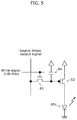
- FIG. 5 is a circuit diagram illustrating one example of a configuration of a sub-pixel in a pixel according to the embodiment.
- FIG. 6 is a diagram illustrating examples of write signals to be input to the sub-pixel according to the embodiment.
- FIG. 7 is a schematic diagram illustrating display state transitions of the display unit according to the embodiment.
- FIG. 8 is a schematic diagram illustrating the configuration of display screen data storage according to the embodiment.
- FIG. 9 is a flow chart indicating a gain calculating method in a gain calculation circuit according to the embodiment.
- FIG. 10 is a flow chart indicating a processing method in a processing circuit according to the embodiment.
- FIG. 11 is a graph indicating a temporal waveform of a current to be supplied to a plurality of pixels when switching from all black display to all white display is made in a display device in a comparative example.
- FIG. 12 is a graph indicating a temporal waveform of a current to be supplied to a plurality of pixels when switching from all black display to all white display is made in the display device according to the embodiment.
- FIG. 13 is a graph indicating the relationship between weight a and luminance IN (n) according to a variation of the embodiment.
- FIG. 14 is a block diagram illustrating a relationship between a processing circuit and a display device according to a variation.
- FIG. 15 is an appearance of a PC which includes the processing circuit according to the variation.
- FIG. 16 is an appearance of a hard disc recorder which includes the processing circuit according to the variation.
- FIG. 17 is a functional block diagram representing a functional configuration of the display device according to the variation.
- FIG. 18 is an appearance of a thin flat TV which includes the display device according to the embodiment.
- FIG. 1 is a functional block diagram illustrating a functional configuration of display device 10 according to the embodiment.
- FIG. 2 is a block diagram illustrating a functional configuration of processing circuit 20 according to the embodiment.
- FIG. 3 is a block diagram illustrating a functional configuration of current limiting circuit 40 included in display device 10 according to the embodiment.
- FIG. 4 is a block diagram illustrating a functional configuration of display panel 60 included in display device 10 according to the embodiment.
- display device 10 includes processing circuit 20 , current limiting circuit 40 , and display panel 60 .
- Processing circuit 20 is a circuit which processes video signals for display device 10 . As illustrated in FIG. 2 , processing circuit 20 includes frame memory 22 and signal processor 24 .
- Frame memory 22 is a storage which stores video signals of a previous frame which is the frame before a current frame to be input to processing circuit 20 .
- the video signals correspond to a plurality of pixels.
- Frame memory 22 is implemented by, for example, a random access memory (RAM).
- Signal processor 24 is a processor which limits the amount of current to be supplied to the plurality of pixels included in display panel 60 by processing video signals to be input to display device 10 . Processing in signal processor 24 and the effects thereof are described later.
- Display panel 60 is a panel which includes the plurality of pixels each having a self light emitting element, and which displays an image corresponding to video signals. As illustrated in FIG. 4 , display panel 60 includes display unit 70 , write processor 62 , source driver 68 , and shift register for writing 64 . Display unit 70 includes the plurality of pixels, and displays the image corresponding to the video signals. Write processor 62 outputs a control signal and a data signal for writing display data to display unit 70 . Source driver 68 outputs the data signal to display unit 70 . Shift register for writing 64 outputs, to display unit 70 , a write signal which is a control signal for writing the data signal to display unit 70 .
- Current limiting circuit 40 is a circuit which limits a current to be supplied to the plurality of pixels included in display panel 60 .
- current limiting circuit 40 limits a current to be supplied to the plurality of pixels when the value of the electric power to be supplied to the plurality of pixels corresponding to the electric power consumption of display panel 60 exceeds a control target electric power value.
- current limiting circuit 40 includes, weighted averaging circuit 42 , horizontal period data calculation circuit 44 , display screen data storage 46 , gain calculation circuit 48 , and gain circuit 50 .
- Weighted averaging circuit 42 is a circuit which calculates a weighted average of pixel values of respective R, G, and B signals. As illustrated in FIG. 3 , weighted averaging circuit 42 multiplies display data of R, G, and B pixels by weighting coefficients according to electric power consumption characteristics of the respective R, G, and B pixels of display unit 70 , and calculates the sum of these multiplication results.
- Horizontal period data calculation circuit 44 calculates horizontal period electric power conversion data corresponding to display data for each of horizontal periods.
- horizontal period data calculation circuit 44 calculates an integrated value or an average value of weighted averages in the horizontal period output by weighted averaging circuit 42 as the horizontal period electric power conversion data (a level integration value).
- Display screen data storage 46 stores electric power conversion data corresponding to one frame.
- display screen data storage 46 stores electric power conversion data corresponding to one frame output by horizontal period data calculation circuit 44 .
- Gain calculation circuit 48 calculates a gain by which the video signal is to be multiplied, based on electric power conversion data stored in display screen data storage 46 and a control target electric power value.
- gain calculation circuit 48 calculates a display screen electric power which is the electric power consumption of the plurality of pixels for one frame, based on the electric power conversion data stored in display screen data storage 46 .
- Gain calculation circuit 48 further calculates, as a gain, the ratio of the control target electric power value relative to the display screen electric power, when the display screen electric power exceeds the control target electric power value. In this case, a gain is less than 1.
- Gain calculation circuit 48 calculates 1 as the gain when the display screen electric power does not exceed the control target electric power value.
- Gain circuit 50 is a circuit which multiplies a video signal by a gain. Gain circuit 50 multiplies the video signal by the gain calculated in gain calculation circuit 48 . In this embodiment, as illustrated in FIG. 3 , each of the R, G, and B signals is multiplied by the gain. In this way, the video signal is multiplied by the gain less than 1 when the display screen electric power exceeds the control target electric power value, the luminance of the video signal can be reduced. Accordingly, a current to be supplied to the plurality of pixels of display panel 60 is limited.
- FIG. 5 is a circuit diagram illustrating one example of the configuration of a sub-pixel in a pixel according to this embodiment.
- FIG. 5 illustrates the sub-pixel including an organic EL element as a self light emitting element.
- the pixel according to this embodiment includes three sub-pixels corresponding respectively to three colours of R, G, and B.
- the sub-pixel illustrated in FIG. 5 is a sub-pixel for emitting red (R) light. It is to be noted that a sub-pixel for emitting green light and a sub-pixel for emitting blue light have the same circuit configuration as that of the circuit illustrated in FIG. 5 .
- the sub-pixel includes thin film transistor (TFT) 81 , capacitor 84 , TFT 82 , and self light emitting element 85 r.
- TFT thin film transistor
- TFT 81 has an end to which a data signal which is an output signal of source driver 68 is input.
- Capacitor 84 is connected to TFT 81 .
- TFT 82 has a control terminal connected to a connection point between TFT 81 and capacitor 84 .
- Self light emitting element 85 r is connected to TFT 82 .
- TFT 81 switches between on and off based on a write signal which is a control signal that is output by shift register for writing 64 .
- a write signal which is a control signal that is output by shift register for writing 64 .
- FIG. 6 is a diagram illustrating one example of a write signal to be input to the sub-pixel according to this embodiment.
- Display device 10 writes data signal output by source driver 68 to display unit 70 by means of a write signal, and emits light on the basis of the pixels in one horizontal line (hereinafter, also simply referred to as a “line”).
- FIG. 7 is a schematic diagram illustrating display state transitions of display unit 70 according to this embodiment.
- display on the display screen transits from time point T 1 to time point T 2 , and from time point T 2 to time point T 3 .
- the mth field display screen is displayed at time point T 1 corresponding to the end of the mth field illustrated in FIG. 7 .
- shift register for writing 64 which outputs a write signal which is a control signal for writing data signal to each pixel outputs a write signal so that scanning is performed from top to bottom of the display screen starting at the beginning part of the display area of display unit 70 .
- FIG. 8 is a schematic diagram illustrating a configuration of display screen data storage 46 according to this embodiment.
- display screen data storage 46 stores horizontal period electric power conversion data for each horizontal line on the display screen of display unit 70 as signal information to be written to display unit 70 .
- the horizontal period electric power conversion data in the ith line is stored in display screen data storage 46 as the ith line electric power value.
- display screen data storage 46 newly re-writes the electric power value to be stored and stores it as the electric power value corresponding to the signal written onto the display screen.
- FIG. 9 is a flow chart indicating a gain calculation method in gain calculation circuit 48 according to this embodiment.
- gain calculation circuit 48 calculates electric power of a display screen based on the horizontal period electric power conversion data stored in display screen data storage 46 (S 1 ).
- the sum of horizontal period electric power conversion data of the respective horizontal lines stored in display screen data storage 46 is calculated as the electric power of the display screen.
- Gain calculation circuit 48 determines whether the calculated display screen electric power exceeds the predetermined control target electric power value (S 2 ). When the display screen electric power does not exceed the control target electric power value, a gain is set to 1 (S 3 ). When the display screen electric power exceeds the control target electric power value, the ratio of the control target electric power value relative to the display screen electric power is calculated as a gain less than 1 (S 4 ).
- the gain calculated by gain calculation circuit 48 is input to gain circuit 50 .
- gain circuit 50 integrating the gain in the video signal, a current to be supplied to the plurality of pixels of display panel 60 is limited when the electric power of the display screen exceeds the control target value.
- FIG. 10 is a flow chart indicating the processing method in processing circuit 20 according to this embodiment.
- video signals of a previous frame which is the frame before a current frame to be input to processing circuit 20 are stored in frame memory 22 of processing circuit 20 (S 10 ).
- the video signals correspond to a plurality of pixels.
- a current video signal is processed by signal processor 24 of processing circuit 20 (S 20 ).
- Step S 20 in which the video signal is processed first, luminance IN (n) represented by a video signal which is included in video signals of the current frame and which corresponds to a pixel included in the plurality of pixels is compared with luminance IN (n ⁇ 1) represented by a video signal which is included in the video signals of the previous frame and which corresponds to the pixel (S 21 ).
- luminance IN (n) represented by the video signal of the current frame is equal to or smaller than luminance IN (n ⁇ 1) represented by the video signal of the previous frame or equal to or smaller than predetermined threshold value TH (Yes in S 21 )
- the video signal of the current frame corresponding to the pixel is output as it is (S 22 ).
- a weighted average of the video signal of the current frame and the video signal of the previous frame both corresponding to the pixel is output (S 23 ).
- signal processor 24 when signal processor 24 according to this embodiment outputs the video signal of the current frame to display panel 60 as it is when luminance IN (n) (n is a natural number) represented by the video signal of the current frame is smaller than or equal to luminance IN (n ⁇ 1) represented by the video signal of the previous frame, the amount of current to be supplied to the pixel does not exceed the amount of current supplied to the previous frame. Accordingly, even when the pixel is caused to emit light having luminance IN (n) corresponding to the video signal of the current frame, no abrupt increase occurs in the amount of current to be supplied to the pixel as described above. For this reason, signal processor 24 outputs the video signal of the current frame as it is.
- threshold value TH can be set to be, for example, approximately 50% of the maximum luminance represented by the video signal.
- luminance IN (n) represented by the video signal of the current frame is smaller than or equal to luminance IN (n ⁇ 1) of the previous frame even when luminance IN (n) is larger than threshold value TH, current can be reduced by current limiting circuit 40 , and thus the video signal does not need to be processed by signal processor 24 .
- luminance IN (n) represented by the video signal of the current frame is larger than luminance IN (n ⁇ 1) represented by the video signal of the previous frame when luminance IN (n) is larger than threshold value TH
- signal processor 24 outputs a weighted average of the video signal of the current frame and the video signal of the previous frame.
- weight a is a constant larger than 0 and smaller than 1.
- a peak current value which appears in a transient response becomes smaller and transient response time becomes longer, as weight a is decreased.
- the peak current value which appears in a transient response becomes larger and transient response time becomes shorter, as weight a is increased. Because of the trade-off, the value of a is determined according to the optimum balance between the peak current allowable for a product and the response time.
- the luminance of the video signal to be output can be reduced below luminance IN (n). Accordingly, a current to be supplied to the pixel can be reduced.
- the video signals are R, G, and B signals
- a sum W (n) obtained by multiplying the display data of respective R, G, and B sub-pixels by corresponding ones of weighting coefficients p, q, and r according to electric power consumption characteristics of the R, G, or B sub-pixels.
- the display data of the respective R, G, and B signals is represented as R (n), G (n), and B (n)
- sum W (n) is represented according to Expression (2) below.
- W ( n ) p ⁇ R ( n )+ q ⁇ G ( n )+ r ⁇ B ( n ) (2)
- the weighted averaging may be performed on each of the R, G, and B signals.
- luminance Y included in the chrominance signal can be used as luminance IN (n).
- processing circuit 20 is capable of reducing a current to be supplied to display panel 60 even when luminance IN (n) represented by a video signal abruptly increases. It is to be noted that a configuration is also conceivable in which processing circuit 20 always outputs a weighted average of luminance IN (n) and luminance IN (n ⁇ 1) irrespective of the value of luminance IN (n). However, this configuration decreases responsibility to changes of video signals. In this embodiment, however, when luminance IN (n) represented by a video signal does not increase or smaller than or equal to predetermined threshold value TH, processing circuit 20 outputs the video signal as it is, and thus it is possible to reduce decrease in response performance to the video signals.
- FIG. 11 is a graph representing a temporal waveform of a current to be supplied to the plurality of pixels when change from all black display to all white display is made in the display device in the comparative example.
- all white display is maintained after all black display of display unit 70 is changed to all white display.
- FIG. 11 also illustrates images (a) to (d) displayed on display unit 70 at respective time points.
- the display device in the comparative example is in an all black display state at time point T 10 indicated at the left end of the graph in FIG. 11 .
- almost zero current is to be supplied to the plurality of pixels in display unit 70 .
- switching from black display to white display is made starting with the top-end line of display unit 70 for each horizontal period of display unit 70 .
- the current upper limit value is a current value corresponding to a control target electric power value for the value of an electric power to be supplied to the plurality of pixels.
- the current upper limit value is 1.2 A.
- the lines disposed at the upper half area of display unit 70 are switched from black display to white display.
- the luminance of the video signal is reduced by current limiting circuit 40 , and thus the luminance of white display decreases from the top-end line toward lower lines.
- the top-end line of display unit 70 represents white display according to the video signal
- display unit 70 represents white display (that is, gray display) with a luminance lower than the luminance represented by the video signal. Subsequently, the pixels disposed at the lower half area of display unit 70 also represent white display with a luminance lower than the luminance represented by the video signal. In this way, at time point T 12 after one vertical period from time point T 10 , as illustrated in image (c) in FIG. 11 , display unit 70 represents all white display in which luminance decreases toward the bottom end of display unit 70 .
- the amount of current to be supplied to the entirety of the plurality of pixels exceeds the current upper limit value.
- the amount of current to be supplied to the entirety of the plurality of pixels is approximately 2.2 A at the maximum.
- the current to be supplied to the plurality of pixels is limited by current limiting circuit 40 also in the one vertical period from time point T 12 .
- the value of current to be supplied to the plurality of pixels at and after time point T 13 is limited to the current upper limit value or below.
- the amount of current to be supplied to the plurality of pixels may dramatically exceed the current upper limit value temporarily.
- FIG. 12 is a graph representing a temporal waveform of a current to be supplied to the plurality of pixels when change from all black display to all white display is made in display device 10 according to this embodiment.
- processing circuit 20 of display device 10 outputs a video signal of a current frame as it is in the case where luminance IN (n) represented by the video signal which is of the current frame and corresponds to the pixel is smaller than or equal to luminance IN (n ⁇ 1) represented by a video signal which is of a previous frame and corresponds to the pixel or is smaller than or equal to predetermined threshold value TH.
- processing circuit 20 outputs a weighted average of the video signal of the current frame and the video signal of the previous frame.
- processing circuit 20 outputs, to display panel 60 and current limiting circuit 40 , a weighted average of the video signal representing all white display of a current frame and the video signal representing all black display of a previous frame, that is, a video signal representing white display with a luminance reduced from the luminance of the video signal of the current frame. For this reason, the value of a current to be supplied to the plurality of pixels during the period from time point T 10 to time point T 12 can be reduced more significantly than the display device in the comparative example as illustrated in FIG. 12 .
- the video signal corresponding to the vertical period from time point T 12 to time point T 13 also represents all white display.
- the video signal of the previous frame stored in frame memory 22 of processing circuit 20 (that is, the video signal corresponding to the vertical period from time point T 10 to time point T 12 in FIG. 12 ) is a video signal representing all white display.
- luminance IN (n) represented by the video signal of the current frame is smaller than or equal to luminance IN (n ⁇ 1) represented by the video signal of the previous frame
- processing circuit 20 outputs the video signal to display panel 60 and current limiting circuit 40 as it is.
- the value of a current to be supplied to the plurality of pixels increases even in the period from time point T 12 to time point T 13 .
- the maximum value of the current to be supplied to the plurality of pixels is reduced significantly relative to the maximum value of current in the comparative example.
- the video signal corresponding to the vertical period from time point T 13 to time point T 14 also keeps representing all white display. Since this video signal is input to processing circuit 20 , processing circuit 20 outputs the video signal representing all white display as it is as in the period from time point T 12 to time point T 13 .
- the current to be supplied to the plurality of pixels is limited by current limiting circuit 40 to which the video signal representing all white display is input. In this way, the value of a current to be supplied to the plurality of pixels at and after time point T 14 is limited to the current upper limit value or below.
- display device 10 is capable of reducing current to be supplied to the plurality of pixels of the display panel also when the luminance represented by a video signal abruptly increases.
- processing circuit 20 A variation of processing circuit 20 according to this embodiment is described.
- weight a to be used in weighted averaging is a constant in order to simplify processing in processing circuit 20
- weight a does not always need to be a constant.
- weight a is a function of luminance IN (n).
- FIG. 13 is a graph representing the relationship between weight a and luminance IN (n) according to this variation.
- weight a is 1 when luminance IN (n) is smaller than or equal to threshold value TH.
- the processing circuit outputs the video signal to be input, as it is.
- weight a decreases with increase in luminance IN (n).
- the processing circuit is capable of outputting a weighted average suitable for luminance IN (n).
- the processing circuit according to this variation is capable of reducing the value of weight a by which the video signal of a current frame is to be multiplied with increase in luminance IN (n), thereby further reducing the amount of current.
- weight a may be a linear function of luminance IN (n), or a non-linear function.
- the minimum value of weight a may be, for example, 0.5 or above. In this way, it is possible to reduce drastic deterioration in response performance of the display device in response to a video signal.
- processing circuit, etc., according to the present disclosure have been described above based on the embodiment, the processing circuit, etc., according to the present disclosure are not limited to the above embodiment.
- the present disclosure encompasses other embodiments that are implemented by combining some of the optional constituent elements in the embodiments, variations that a person skilled in the art may arrive at by adding various kinds of modifications to the above embodiments within the scope of the present disclosure, or various kinds of apparatuses which include the processing circuit according to any of the embodiments.
- FIG. 14 is a block diagram illustrating the relationship between processing circuit 20 and display device 210 according to this variation.
- processing circuit 20 is included in graphics processing unit (GPU) 212 .
- GPU 212 is a computation device for image processing, receives a video signal as an input, and outputs a video signal processed by processing circuit 20 .
- GPU 212 is disposed outside display device 210 , and outputs the video signal processed by processing circuit 20 to display device 210 .
- GPU 212 may be included in a personal computer (PC) 804 as illustrated in FIG. 15 .
- PC personal computer
- PC 804 is operated by keyboards 806 , mouse 807 , etc.
- Display device 210 may be included in monitor 805 illustrated in FIG. 15 .
- Monitor 805 includes display device 210 , and displays a video signal from PC 804 .
- GPU 212 may be included in hard disc recorder 808 as illustrated in FIG. 16 .
- processing circuit 20 is not included in the display device as described above, the same advantages as provided by processing circuit 20 according to the embodiment are also provided.
- FIG. 17 is a functional block diagram indicating a functional configuration of display device 310 according to a variation. As illustrated in FIG. 17 , display device 310 according to this variation includes processing circuit 20 , current limiting circuit 40 , and display panel 60 , as in display device 10 according to the above embodiment. Display device 310 according to this variation further includes pixel count matching circuit 30 .
- Pixel count limiting circuit 30 is a circuit which receives video signals output from processing circuit 20 , and outputs, to current limiting circuit 40 , matching video signals obtained by matching the pixel count of the video signals to the pixel count of display panel 60 .
- the video signals to processing circuit 20 are high-definition (HD) signals (of 1920 ⁇ 1080 pixels)
- the pixels of display panel 60 are 4 k pixels (3840 ⁇ 2160 pixels)
- an enlargement circuit which increases the pixel count of the video signals is used as pixel count matching circuit 30 .
- a reduction circuit which reduces the pixel count of the video signals is used as pixel count matching circuit 30 .
- pixel count matching circuit 30 may be included at GPU 212 side, or at display device 210 side.
- pixel count matching circuit 30 may switch processing according to the pixel count of video signals to be input.
- pixel count matching circuit 30 may increase the pixel count of the video signals by the enlargement circuit when the pixel count of the video signals needs to be increased, reduce the pixel count of the video signals by the reduction circuit when the pixel count of the video signals needs to be reduced, and output the video signal as it is (without changing the pixel count of the video signals) when there is no need to change the pixel count of the video signals.
- Such process switching may be automatically performed based on the format of a video signal and pixel count information of display panel 60 which has been obtained in advance.
- the display device according to the embodiment may be embedded in thin flat TV 802 as illustrated in FIG. 18 . Even in this case, advantages similar to those obtainable in the above embodiment are provided.
- each of the pixels of the display panel includes three sub-pixels corresponding respectively to R, G, and B colours.
- the pixel configuration is not limited thereto.
- each of the pixels may include four sub-pixels corresponding respectively to R, G, B, and W colours.
- the pixels may include a single circuit as illustrated in FIG. 5 .
- the video signals are RGB signals
- the video signals may include signals other than the RGB signals. In other words, it is only necessary that video signals include RGB signals.
- video signals are not limited to signals including RGB signals.
- video signals may be chrominance signals including luminance signals.
- luminance Y included in a chrominance signal can be used as luminance IN (n).
- organic EL elements are used as self light emitting elements in the above embodiment, self light emitting elements are not limited thereto.
- inorganic EL elements or the like may be used as self light emitting elements.
- the present disclosure is useful for organic EL flat panel displays, and is particularly suitable for use in displays with a large display screen which consume large electric power.
Landscapes
- Engineering & Computer Science (AREA)
- Physics & Mathematics (AREA)
- Computer Hardware Design (AREA)
- General Physics & Mathematics (AREA)
- Theoretical Computer Science (AREA)
- Multimedia (AREA)
- Signal Processing (AREA)
- Control Of Indicators Other Than Cathode Ray Tubes (AREA)
- Electroluminescent Light Sources (AREA)
- Control Of El Displays (AREA)
Abstract
Description
a×IN(n)+(1−a)×IN(n−1) (1)
W(n)=p×R(n)+q×G(n)+r×B(n) (2)
Claims (9)
a×IN(n)+(1−a)×IN(n−1) (1)
Applications Claiming Priority (3)
| Application Number | Priority Date | Filing Date | Title |
|---|---|---|---|
| JP2019-013493 | 2019-01-29 | ||
| JPJP2019-013493 | 2019-01-29 | ||
| JP2019013493A JP7181597B2 (en) | 2019-01-29 | 2019-01-29 | Processing circuit, display device, and processing method |
Publications (2)
| Publication Number | Publication Date |
|---|---|
| US20200279528A1 US20200279528A1 (en) | 2020-09-03 |
| US11100859B2 true US11100859B2 (en) | 2021-08-24 |
Family
ID=71992595
Family Applications (1)
| Application Number | Title | Priority Date | Filing Date |
|---|---|---|---|
| US16/774,743 Active US11100859B2 (en) | 2019-01-29 | 2020-01-28 | Processing circuit, display device, and processing method for reducing current during luminance change |
Country Status (2)
| Country | Link |
|---|---|
| US (1) | US11100859B2 (en) |
| JP (1) | JP7181597B2 (en) |
Cited By (1)
| Publication number | Priority date | Publication date | Assignee | Title |
|---|---|---|---|---|
| US20230169920A1 (en) * | 2021-11-26 | 2023-06-01 | Joled Inc. | Current limiting circuit, display device, and current limiting method |
Families Citing this family (4)
| Publication number | Priority date | Publication date | Assignee | Title |
|---|---|---|---|---|
| JP7594863B2 (en) * | 2020-05-22 | 2024-12-05 | JDI Design and Development 合同会社 | Display device and current limiting method |
| JP2023108808A (en) * | 2022-01-26 | 2023-08-07 | 株式会社Joled | CURRENT LIMITING CIRCUIT, DISPLAY DEVICE AND CURRENT LIMITING METHOD |
| IT202200018054A1 (en) * | 2022-09-02 | 2024-03-02 | Macropix S R L | Method to optimize energy consumption of LED screens. |
| KR20240141888A (en) * | 2023-03-20 | 2024-09-30 | 삼성디스플레이 주식회사 | Display device and method of driving the same |
Citations (3)
| Publication number | Priority date | Publication date | Assignee | Title |
|---|---|---|---|---|
| JP2007212644A (en) | 2006-02-08 | 2007-08-23 | Matsushita Electric Ind Co Ltd | Self-luminous display device |
| US20120069062A1 (en) * | 2009-06-10 | 2012-03-22 | Sharp Kabushiki Kaisha | Driving Device, Driving Method, Image Display Device, Television Receiver, Display Monitor Device, Program And Record Medium |
| US20140198091A1 (en) * | 2013-01-17 | 2014-07-17 | Samsung Display Co., Ltd. | Organic light emitting display |
Family Cites Families (5)
| Publication number | Priority date | Publication date | Assignee | Title |
|---|---|---|---|---|
| JP3592126B2 (en) * | 1999-02-26 | 2004-11-24 | キヤノン株式会社 | Image display device and control method thereof |
| FR2929795B1 (en) * | 2008-04-03 | 2010-09-24 | Irts | METHOD FOR CONVERTING A VIDEO SIGNAL FOR SCINTLING COMPENSATION, AND CONVERSION DEVICE THEREFOR |
| JP4468467B2 (en) * | 2008-06-27 | 2010-05-26 | 株式会社東芝 | Video signal control device, video display system, and video signal control method |
| JP6167324B2 (en) * | 2012-07-25 | 2017-07-26 | 株式会社Joled | Display device, image processing device, and image processing method |
| JP7222723B2 (en) * | 2019-01-17 | 2023-02-15 | 株式会社ジャパンディスプレイ | Display device |
-
2019
- 2019-01-29 JP JP2019013493A patent/JP7181597B2/en active Active
-
2020
- 2020-01-28 US US16/774,743 patent/US11100859B2/en active Active
Patent Citations (3)
| Publication number | Priority date | Publication date | Assignee | Title |
|---|---|---|---|---|
| JP2007212644A (en) | 2006-02-08 | 2007-08-23 | Matsushita Electric Ind Co Ltd | Self-luminous display device |
| US20120069062A1 (en) * | 2009-06-10 | 2012-03-22 | Sharp Kabushiki Kaisha | Driving Device, Driving Method, Image Display Device, Television Receiver, Display Monitor Device, Program And Record Medium |
| US20140198091A1 (en) * | 2013-01-17 | 2014-07-17 | Samsung Display Co., Ltd. | Organic light emitting display |
Cited By (2)
| Publication number | Priority date | Publication date | Assignee | Title |
|---|---|---|---|---|
| US20230169920A1 (en) * | 2021-11-26 | 2023-06-01 | Joled Inc. | Current limiting circuit, display device, and current limiting method |
| US12020644B2 (en) * | 2021-11-26 | 2024-06-25 | Jdi Design And Development G.K. | Current limiting circuit, display device, and current limiting method |
Also Published As
| Publication number | Publication date |
|---|---|
| US20200279528A1 (en) | 2020-09-03 |
| JP2020122836A (en) | 2020-08-13 |
| JP7181597B2 (en) | 2022-12-01 |
Similar Documents
| Publication | Publication Date | Title |
|---|---|---|
| US11100859B2 (en) | Processing circuit, display device, and processing method for reducing current during luminance change | |
| US10311799B2 (en) | Display device and method for controlling peak luminance of the same | |
| US10699615B2 (en) | Application processor and display device including the same | |
| US10553146B2 (en) | Display device and method of driving the same | |
| US9711080B2 (en) | Timing controller, driving method thereof, and display device using the same | |
| KR102370367B1 (en) | Display apparatus and method of driving the same | |
| US11107403B2 (en) | Current limiting circuit, display device, and current limiting method | |
| US20140002511A1 (en) | Image display device capable of supporting brightness enchancement and power control and method thereof | |
| JP4451057B2 (en) | Display device driving method, display device, and program thereof | |
| KR20200128283A (en) | Display device and driving method of the same | |
| US11942031B2 (en) | Current limiting circuit, display device, and current limiting method | |
| US11893932B2 (en) | Display apparatus and current limiting method | |
| CN116597762A (en) | display device | |
| US20230169920A1 (en) | Current limiting circuit, display device, and current limiting method | |
| US20140368531A1 (en) | Dynamic contrast enhancement using dithered gamma remapping | |
| KR20160078535A (en) | Display device and method for driving thereof | |
| US10163407B2 (en) | Display and scanning method thereof | |
| JP7305179B2 (en) | CURRENT LIMITING CIRCUIT, DISPLAY DEVICE AND CURRENT LIMITING METHOD | |
| JP2010160237A (en) | Method for generating light emission control signal, circuit for generating light emission control signal, display device, and electronic equipment | |
| US20100309099A1 (en) | Display device and driving method thereof | |
| JP4503669B2 (en) | Display device driving method, display device, and program thereof | |
| JP2021060557A (en) | Current limit circuit, display device, and current limit method | |
| JP2024139253A (en) | Current limiting circuit, display device, and current limiting method | |
| KR102379774B1 (en) | Image processing method, image processing circuit and display device using the same | |
| JP2006145718A (en) | Electro-optical device drive circuit and method, electro-optical device, and electronic apparatus including the same |
Legal Events
| Date | Code | Title | Description |
|---|---|---|---|
| FEPP | Fee payment procedure |
Free format text: ENTITY STATUS SET TO UNDISCOUNTED (ORIGINAL EVENT CODE: BIG.); ENTITY STATUS OF PATENT OWNER: LARGE ENTITY |
|
| AS | Assignment |
Owner name: JOLED INC., JAPAN Free format text: ASSIGNMENT OF ASSIGNORS INTEREST;ASSIGNOR:KATO, TOSHIYUKI;REEL/FRAME:052750/0557 Effective date: 20200303 |
|
| STPP | Information on status: patent application and granting procedure in general |
Free format text: NON FINAL ACTION MAILED |
|
| STPP | Information on status: patent application and granting procedure in general |
Free format text: RESPONSE TO NON-FINAL OFFICE ACTION ENTERED AND FORWARDED TO EXAMINER |
|
| STPP | Information on status: patent application and granting procedure in general |
Free format text: NOTICE OF ALLOWANCE MAILED -- APPLICATION RECEIVED IN OFFICE OF PUBLICATIONS |
|
| STPP | Information on status: patent application and granting procedure in general |
Free format text: PUBLICATIONS -- ISSUE FEE PAYMENT RECEIVED |
|
| STPP | Information on status: patent application and granting procedure in general |
Free format text: PUBLICATIONS -- ISSUE FEE PAYMENT VERIFIED |
|
| STCF | Information on status: patent grant |
Free format text: PATENTED CASE |
|
| AS | Assignment |
Owner name: INCJ, LTD., JAPAN Free format text: SECURITY INTEREST;ASSIGNOR:JOLED, INC.;REEL/FRAME:063396/0671 Effective date: 20230112 |
|
| AS | Assignment |
Owner name: JOLED, INC., JAPAN Free format text: CORRECTION BY AFFIDAVIT FILED AGAINST REEL/FRAME 063396/0671;ASSIGNOR:JOLED, INC.;REEL/FRAME:064067/0723 Effective date: 20230425 |
|
| AS | Assignment |
Owner name: JDI DESIGN AND DEVELOPMENT G.K., JAPAN Free format text: ASSIGNMENT OF ASSIGNORS INTEREST;ASSIGNOR:JOLED, INC.;REEL/FRAME:066382/0619 Effective date: 20230714 Owner name: JDI DESIGN AND DEVELOPMENT G.K., JAPAN Free format text: ASSIGNMENT OF ASSIGNOR'S INTEREST;ASSIGNOR:JOLED, INC.;REEL/FRAME:066382/0619 Effective date: 20230714 |
|
| MAFP | Maintenance fee payment |
Free format text: PAYMENT OF MAINTENANCE FEE, 4TH YEAR, LARGE ENTITY (ORIGINAL EVENT CODE: M1551); ENTITY STATUS OF PATENT OWNER: LARGE ENTITY Year of fee payment: 4 |
|
| AS | Assignment |
Owner name: MAGNOLIA BLUE CORPORATION, JAPAN Free format text: ASSIGNMENT OF ASSIGNORS INTEREST;ASSIGNOR:JDI DESIGN AND DEVELOPMENT G.K.;REEL/FRAME:072039/0656 Effective date: 20250625 Owner name: MAGNOLIA BLUE CORPORATION, JAPAN Free format text: ASSIGNMENT OF ASSIGNOR'S INTEREST;ASSIGNOR:JDI DESIGN AND DEVELOPMENT G.K.;REEL/FRAME:072039/0656 Effective date: 20250625 |