US11095093B2 - Laser driver with high-speed and high-current and current modulating method thereof - Google Patents
Laser driver with high-speed and high-current and current modulating method thereof Download PDFInfo
- Publication number
- US11095093B2 US11095093B2 US16/740,468 US202016740468A US11095093B2 US 11095093 B2 US11095093 B2 US 11095093B2 US 202016740468 A US202016740468 A US 202016740468A US 11095093 B2 US11095093 B2 US 11095093B2
- Authority
- US
- United States
- Prior art keywords
- nmosfet
- drain
- electrically connecting
- driving unit
- circuit
- Prior art date
- Legal status (The legal status is an assumption and is not a legal conclusion. Google has not performed a legal analysis and makes no representation as to the accuracy of the status listed.)
- Active
Links
- 238000000034 method Methods 0.000 title abstract description 16
- 238000006243 chemical reaction Methods 0.000 claims abstract description 12
- 239000003990 capacitor Substances 0.000 claims description 46
- 238000013461 design Methods 0.000 abstract description 3
- 238000004891 communication Methods 0.000 description 4
- 238000010586 diagram Methods 0.000 description 4
- 238000012986 modification Methods 0.000 description 2
- 230000004048 modification Effects 0.000 description 2
- 230000005693 optoelectronics Effects 0.000 description 2
- 238000012545 processing Methods 0.000 description 2
- 230000000630 rising effect Effects 0.000 description 2
- 239000004065 semiconductor Substances 0.000 description 2
- 238000012546 transfer Methods 0.000 description 2
- 230000008033 biological extinction Effects 0.000 description 1
- 238000011161 development Methods 0.000 description 1
- 230000000694 effects Effects 0.000 description 1
- 239000000835 fiber Substances 0.000 description 1
- 238000004519 manufacturing process Methods 0.000 description 1
- 230000003287 optical effect Effects 0.000 description 1
- 239000013307 optical fiber Substances 0.000 description 1
- 229920006395 saturated elastomer Polymers 0.000 description 1
- 230000006641 stabilisation Effects 0.000 description 1
- 238000011105 stabilization Methods 0.000 description 1
Images


Classifications
-
- H—ELECTRICITY
- H01—ELECTRIC ELEMENTS
- H01S—DEVICES USING THE PROCESS OF LIGHT AMPLIFICATION BY STIMULATED EMISSION OF RADIATION [LASER] TO AMPLIFY OR GENERATE LIGHT; DEVICES USING STIMULATED EMISSION OF ELECTROMAGNETIC RADIATION IN WAVE RANGES OTHER THAN OPTICAL
- H01S5/00—Semiconductor lasers
- H01S5/04—Processes or apparatus for excitation, e.g. pumping, e.g. by electron beams
- H01S5/042—Electrical excitation ; Circuits therefor
- H01S5/0427—Electrical excitation ; Circuits therefor for applying modulation to the laser
-
- H—ELECTRICITY
- H01—ELECTRIC ELEMENTS
- H01S—DEVICES USING THE PROCESS OF LIGHT AMPLIFICATION BY STIMULATED EMISSION OF RADIATION [LASER] TO AMPLIFY OR GENERATE LIGHT; DEVICES USING STIMULATED EMISSION OF ELECTROMAGNETIC RADIATION IN WAVE RANGES OTHER THAN OPTICAL
- H01S5/00—Semiconductor lasers
- H01S5/04—Processes or apparatus for excitation, e.g. pumping, e.g. by electron beams
- H01S5/042—Electrical excitation ; Circuits therefor
- H01S5/0428—Electrical excitation ; Circuits therefor for applying pulses to the laser
Definitions
- the present invention relates to an optoelectronic integrated circuit (OEIC), and more particularly to a laser driver with high-speed and high-current and current modulating method thereof.
- OEIC optoelectronic integrated circuit
- a laser driver is a key circuit of an optoelectronic integrated circuit in a fiber communication system. It's important for outputting quality optical signals with the laser driver has high bandwidth and the modulated current intensity. In order to work with high-speed without inter-symbol interference (ISI), the laser driver needs sufficient bandwidth. In order to get enough modulated current to ensure outputting big extinction ratio, the laser driver must also be with proper gain.
- ISI inter-symbol interference
- pins of the laser driver are in bigger sizes, or input signals of the laser driver have higher amplitude.
- the amplitude of the input signals always has been limited, and work speed of the laser driver will be limited by high input capacitance because the bigger the sizes of pins are, the bigger input capacitance will be.
- the laser driver with high-current uses passive inductors peaking mode or active negative feedback mode to improve circuit bandwidth.
- passive inductors peaking mode both the expenditure of chip area and the production costs will be increased significantly.
- active negative feedback mode will not only has high cost, but also cause stabilization problems.
- the traditional high-current laser driver usually uses cascading of two-stage amplifiers, it has a problem of the common mode voltage.
- the object of the present invention is to provide a laser driver with high-speed and high-current to solve the problem of lack of bandwidth.
- the laser driver with high-speed and high-current receives high-speed differential data signals, and outputs differential drive voltage signal after processing the differential data signals by negative capacitance technique, so as to improve the bandwidth of the laser driver.
- Another object of the present invention is to provide a current modulation method about a laser driver with high-speed and high-current to obtain a modulation current for the laser driver.
- the present invention provides a laser driver with high-speed and high-current, receiving a pair of high-speed differential data signals V in1 , V in2 , and outputting a differential drive voltage signal V 0 ;
- the laser driver includes a first driving unit and a second driving unit; each driving unit includes a pre-drive amplifier circuit and a main drive amplifier circuit;
- the pre-drive amplifier circuit includes:
- the main drive amplifier circuit includes:
- the gates of the NMOSFETs M 1A and M 1B of the first driving unit are used for receiving the signals V in1
- the gates of the NMOSFETs M 1A and M 1B of the second driving unit are used for receiving the signals V in2
- the drain of the NMOSFET M 2A of the first driving unit is electrically connected to the drain of the NMOSFET M 2A of the second driving unit
- the drain of the NMOSFET M 2B of the first driving unit is electrically connected to the drain of the NMOSFET M 2B of the second driving unit
- two connection ends are connected to the connection of the NMOSFET M 2A of the first driving unit and the second driving unit and the connection of the NMOSFET M 2B of the first driving unit and the second driving unit, respectively, the two connection ends serves as the outputs of the signal V 0 .
- the resistance values of the resistors R 1 and R 2 are equal to 100 ⁇ .
- the capacitance value of the capacitor C F1 is equal to the capacitance value of the capacitor C F2 .
- the size of the NMOSFET of the second driving unit is smaller than the size of the NMOSFET of the first driving unit.
- the two connection ends are electrically connected with an external resistor, the signal V 0 is directly modulated by the typical input impedance of the laser.
- the present invention also provides a laser driver with high-speed and high-current, receiving a pair of high-speed differential data signals V in1 , V in2 , and outputting a differential drive voltage signal V 0 ;
- the laser driver includes a first driving unit and a second driving unit; each driving unit includes a pre-drive amplifier circuit and a main drive amplifier circuit;
- the pre-drive amplifier circuit includes:
- the first differential transistor pair circuit includes NMOSFETs M 1A and M 1B ; the gates of the NMOSFETs M 1A and M 1B of the first driving unit being used for receiving the signals V in1 , the gates of the NMOSFETs M 1A and M 1B of the second driving unit being used for receiving the signals V in2 ; the drains of the NMOSFETs M 1A and M 1B are electrically connected to the differential voltage conversion circuit.
- the differential voltage conversion circuit includes resistors R p1 and R p2
- the DC common mode level reduction circuit includes a resistor R s1 ; one end of the resistor R p1 electrically connecting the drain of the NMOSFET M 1A , one end of the resistor R p2 is electrically connected to the drain of the NMOSFET M 1B ; one end of the resistor R s1 electrically connecting the other ends of the resistors R p1 and R p2 , the other end of the resistor R s1 electrically connecting ground.
- the first cascode current mirror circuit includes NMOSFETs M 5 , M 6 , M 7 and M 8 ; the gate and the drain of the NMOSFET M 5 are electrically connected, and receiving a current Isi; the gate and the drain of the NMOSFET M 6 are electrically connected, and electrically connected to the source of the NMOSFET M 5 ; the source of the NMOSFET M 6 receiving a voltage V SS ; the gates of the NMOSFETs M 7 and M 5 are electrically connected, the drain of the NMOSFET M 7 electrically connected to the sources of the NMOSFETs M 1A and M 1B ; the gates of the NMOSFETs M 8 and M 6 are electrically connected, the drain of the NMOSFET M 8 is electrically connected to the source of the NMOSFET M 7 , the source of the NMOSFET M 8 receiving the voltage V SS .
- the second differential transistor pair circuit includes NMOSFETs M 2A and M 2B ; the gate of the NMOSFET M 2A is electrically connected to the drain of the NMOSFET M 1B , the gate of the NMOSFET M 2B is electrically connected to the drain of the NMOSFET M 1A ; the drains of the NMOSFETs M 2A and M 2B are electrically connected to the matching circuit.
- the bandwidth boost circuit includes capacitors C F1 and C F2 ; one end of the capacitor C F1 is electrically connected to the gate of the NMOSFET M 2A , the other end of the capacitor C F1 is electrically connected to the drain of the NMOSFET M 2B ; one end of the capacitor C F2 is electrically connected to the gate of the NMOSFET M 2B , the other end of the capacitor C F2 is electrically connected to the drain of the NMOSFET M 2A .
- the matching circuit includes resistors R 1 and R 2 ; one end of the resistor R 1 is electrically connected to the drain of the NMOSFET M 2A , the other end of the resistor R 1 is electrically connected to the ground; one end of the resistor R 2 is electrically connected to the drain of the NMOSFET M 2B , the other end of the resistor R 2 is electrically connected to the ground.
- the drain of the NMOSFET M 2A of the first driving unit is electrically connected to the drain of the NMOSFET M 2A of the second driving unit
- the drain of the NMOSFET M 2B of the first driving unit is electrically connected to the drain of the NMOSFET M 2B of the second driving unit
- two connection ends are connected to the connection of the NMOSFET M 2A of the first driving unit and the second driving unit and the connection of the NMOSFET M 2B of the first driving unit and the second driving unit, respectively, the two connection ends serves as the outputs of the signal V 0 .
- the second cascode current mirror circuit includes NMOSFETs M 9 , M 10 , M 11 and M 12 ; the gate and the drain of the NMOSFET M 9 are electrically connected, and receiving a current I B2 ; the gate and the drain of the NMOSFET M 10 are electrically connected, and electrically connected to the source of the NMOSFET M 9 ; the source of the NMOSFET M 10 is receiving the voltage V SS ; the gates of the NMOSFETs M 11 and M 9 are electrically connected, the drain of the NMOSFET M 11 is electrically connected to the sources of the NMOSFETs M 2A and M 2B ; the gates of the NMOSFETs M 12 and M 10 are electrically connected, the drain of the NMOSFET M 12 is electrically connected to the source of the NMOSFET M 11 , the source of the NMOSFET M 12 receiving the voltage V SS .
- the two connection ends are electrically connected with an external resistor, the signal V 0 is directly modulated by the typical input impedance of the laser.
- the signal V 0 is directly modulated by a four-level Pulse Amplitude Modulated mode.
- the present invention also provides a current modulation method about a laser driver with high-speed and high-current;
- the laser driver is used for receiving a pair of high-speed differential data signals V in1 , V in2 , and outputting a differential drive voltage signal V 0 ;
- the laser driver includes a first driving unit and a second driving unit; each driving unit includes a pre-drive amplifier circuit and a main drive amplifier circuit;
- the pre-drive amplifier circuit includes:
- the main drive amplifier circuit includes:
- the current modulation method includes:
- the first driving unit when the resistance value of the external resistor being equal to 25 ⁇ , the first driving unit is able to provide a maximum modulation current of 80 mA, the second driving unit is able to provide a maximum modulation current of 40 mA; when the resistance value of the external resistor is equal to 50 ⁇ , the first driving unit is able to provide a maximum modulation current of 60 mA, the second driving unit is able to provide a maximum modulation current of 30 mA.
- the two driving units when both the currents I B1 and I B2 are valid, the two driving units is able to provide a maximum modulation current of 120 mA.
- the first differential transistor pair circuit includes NMOSFETs M 1A and M 1B ; the gates of the NMOSFETs M 1A and M 1B of the first driving unit are used for receiving the signals V in1 , the gates of the NMOSFETs M 1A and M 1B of the second driving unit are used for receiving the signals V in2 ;
- the differential voltage conversion circuit includes resistors R p1 and R p2 ,
- the DC common mode level reduction circuit includes a resistor R s1 ; one end of the resistor R p1 is electrically connected to the drain of the NMOSFET M 1A , one end of the resistor R p2 is electrically connected to the drain of the NMOSFET M 1B ; one end of the resistor R s1 is electrically connected to the other ends of the resistors R p1 and R p2 , the other end of the resistor R s1 is electrically connected to the ground;
- the first cascode current mirror circuit includes NMOSFET
- the solution of the present invention for solving the above problem, is to apply the laser driver with high-speed and high-current which receives high-speed differential data signals, and output differential drive voltage signal after processing the differential data signals by negative capacitance technique.
- the present invention avoids the enhancement of chip area caused by the use of passive inductors peaking mode to enhance bandwidth, and reduces the cost of chip. It does not need to use buffer level circuit to realize DC level transfer, which reduces design complexity and circuit power consumption in the present invention.
- the negative capacitance technique is applied to optimize the circuit bandwidth, so as to ensure the working speed of the circuit, and the present invention uses two driving units with similar structure to realize a circuit that can be applied to NRZ modulated direct modulation laser, indirect modulation laser and four-level modulation transmitter.
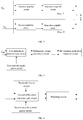
- FIG. 1 is a circuit diagram of the laser driver with high-speed and high-current, according to the first embodiment of the present invention.
- FIG. 2 is a module diagram of the laser driver with high-speed and high-current, according to the second embodiment of the present invention.
- FIG. 3 is a module diagram of the pre-drive amplifier circuit of the laser driver, according to the second embodiment of the present invention.
- FIG. 4 is a module diagram of the main drive amplifier circuit of the laser driver, according to the second embodiment of the present invention.
- a laser driver with high-speed and high-current is shown as an embodiment.
- the laser driver is used for receiving a pair of high-speed differential data signals V in1 , V in2 , and outputting a differential drive voltage signal V 0 .
- the laser driver includes a first driving unit (Slice I) and a second driving unit (Slice II), and each driving unit includes a pre-drive amplifier circuit and a main drive amplifier circuit.
- the pre-drive amplifier circuit includes six n-type metal-oxide-semiconductors (NMOSFETs M 1A , M 1B , M 5 ⁇ M 8 ) and three resistors (resistors R p1 , R p2 , R s1 ).
- NMOSFETs M 1A , M 1B , M 5 ⁇ M 8 n-type metal-oxide-semiconductors
- resistors resistors
- One end of the resistor R p1 is electrically connected to the drain of the NMOSFET M 1A , the other end of the resistor R p1 is electrically connected to one end of the resistor R s1 .
- One end of the resistor R p2 is electrically connected to the drain of the NMOSFET M 1B , the other end of the resistor R p2 is electrically connected to one end of the resistor R s1 , the other end of the resistor R s1 is electrically connected to ground.
- the NMOSFETs M 1A and M 1B are differential input transistors, the gates of the NMOSFETs M 1A and M 1B of the first driving unit are used for receiving the signals V in1 , the gates of the NMOSFETs M 1A and M 1B of the second driving unit are used for receiving the signals V in2 .
- the gate and the drain of the NMOSFET M 5 are electrically connected, and is used for receiving a current I B1 .
- the gate and the drain of the NMOSFET M 6 are electrically connected, and connected to the source of the NMOSFET M 5 electrically.
- the source of the NMOSFET M 6 is used to receive a voltage V SS .
- the gates of the NMOSFETs M 7 and M 5 are electrically connected, and the drain of the NMOSFET M 7 electrically is connected to the sources of the NMOSFETs M 1A and M 1B .
- the gates of the NMOSFETs M 8 and M 6 are electrically connected, the drain of the NMOSFET M 8 is electrically connected to the source of the NMOSFET M 7 , and the source of the NMOSFET M 8 is used for receiving the voltage V SS .
- the main function of the resistor R s1 is to reduce the DC common mode level of the output of the pre-drive amplifier circuit, so that the differential input transistor of the main drive amplifier circuit can work in a saturated state.
- the NMOSFETs M 8 ⁇ M 8 form a cascode current mirror.
- the NMOSFETs M 1A and M 1B are a pair of differential transistors, they convert the data signals V in1 and V in2 into differential current, which is then converted into a differential voltage output through two resistors R p1 and sent to the next stage.
- the main drive amplifier circuit includes six n-type metal-oxide-semiconductors (NMOSFETs M 2A , M 2B , M 9 ⁇ M 12 ), two resistors (resistors R 1 , R 2 ) and two capacitors (capacitors C F1 , C F2 ).
- NMOSFETs M 2A , M 2B , M 9 ⁇ M 12 n-type metal-oxide-semiconductors
- resistors resistors
- capacitors capacitors
- the gate of the NMOSFET M 2A is electrically connected to the drain of the NMOSFET M 1B
- the gate of the NMOSFET M 2B is electrically connected to the drain of the NMOSFET M 1A
- the drain of the NMOSFET M 2A of the first driving unit is electrically connected to the drain of the NMOSFET M 2A of the second driving unit
- the drain of the NMOSFET M 2B of the first driving unit is electrically connected to the drain of the NMOSFET M 2B of the second driving unit
- two connection ends are connected to the connection of the NMOSFET M 2A of the first driving unit and the second driving unit and the connection of the NMOSFET M 2B of the first driving unit and the second driving unit, respectively, the two connection ends serves as the outputs of the signal V 0 .
- One end of the resistor R 1 is electrically connected to the drain of the NMOSFET M 2A , the other end of the resistor R 1 is electrically connected to ground.
- One end of the resistor R 2 is electrically connected to the drain of the NMOSFET M 2B , the other end of the resistor R 2 is electrically connected to the ground.
- One end of the capacitor C F1 is electrically connected to the gate of the NMOSFET M 2A
- the other end of the capacitor C F1 is electrically connected to the drain of the NMOSFET M 2B .
- One end of the capacitor C F2 is electrically connected to the gate of the NMOSFET M 2B , the other end of the capacitor C F2 is electrically connected to the drain of the NMOSFET M 2A .
- the gate and the drain of the NMOSFET M 9 are electrically connected, and is used for receiving a current I B2 .
- the gate and the drain of the NMOSFET M 10 are electrically connected, and electrically connect the source of the NMOSFET M 9 .
- the source of the NMOSFET M 10 is used for receiving the voltage V SS .
- the gates of the NMOSFETs M 11 and M 9 are electrically connected, the drain of the NMOSFET M 11 is electrically connected to the sources of the NMOSFETs M 2A and M 2B .
- the gates of the NMOSFETs M 12 and M 10 are electrically connected, the drain of the NMOSFET M 12 are electrically connected to the source of the NMOSFET M 11 , the source of the NMOSFET M 12 is used for receiving the voltage V SS .
- the function of the capacitor C F1 is to improve the rising and falling speed of the output signal edge by using positive feedback, and reduce the large input capacitance caused by Miller effect and thus improve the bandwidth.
- the two resistors with a resistance value of 100 ⁇ are able to effectively suppress the ringing caused by the binding line inductance and complete the impedance matching of the output.
- the NMOSFETs M 2A and M 2B further amplify the output signal of the main drive amplifier circuit.
- the NMOSFETs M 9 ⁇ M 12 form a cascode current mirror to provide output modulation current.
- the size of the NMOSFET of the Slice II is smaller than the size of the NMOSFET of the Slice I.
- the Slice I and the Slice II modulate the current by controlling the sizes of two external reference current sources to make one external reference current source valid and the other external reference current source invalid or both the two external reference current sources valid.
- the two connection ends are electrically connected with an external resistor, the signal V 0 is directly modulated by the typical input impedance of the laser.
- the resistance value of the external resistor is equal to 25 ⁇
- the Slice I is able to provide a maximum modulation current of 80 mA
- the Slice II is able to provide a maximum modulation current of 40 mA.
- the resistance value of the external resistor is equal to 50
- the Slice I is able to provide a maximum modulation current of 60 mA
- the Slice II is able to provide a maximum modulation current of 30 mA
- the two driving units modulate the signal V 0 directly by a four-level Pulse Amplitude Modulated mode (PAM4), the two driving units are able to provide a maximum modulation current of 120 mA.
- PAM4 Pulse Amplitude Modulated mode
- the laser driver with high-speed and high-current receives high-speed differential data signals, and outputs differential drive voltage signal after processed the differential data signals by negative capacitance technique.
- This embodiment avoids the enhancement of chip area caused by the use of passive inductors peaking mode to enhance bandwidth, and reduces the cost of chip. It does not need to use buffer level circuit to realize DC level transfer, and reduces design complexity and circuit power consumption in this embodiment.
- the negative capacitance technique is applied to optimize the circuit bandwidth, so as to ensure the working speed of the circuit, and this embodiment uses two driving units with similar structure to realize the circuit can be applied to NRZ modulated direct modulation laser, indirect modulation laser and four-level modulation transmitter.
- the laser driver is used for receiving a pair of high-speed differential data signals V in1 , V in2 , and outputting a differential drive voltage signal V 0 .
- the laser driver includes a first driving unit (Slice I) and a second driving unit (Slice II), and each driving unit includes a pre-drive amplifier circuit and a main drive amplifier circuit.
- the pre-drive amplifier circuit includes a first differential transistor pair circuit, a differential voltage conversion circuit, a DC common mode level reduction circuit and a first cascode current mirror circuit.
- the first differential transistor pair circuit is used for converting one high-speed differential data signal into a first differential current signal.
- the first differential transistor pair circuit can include the NMOSFETs M 1A and M 1B in the first embodiment.
- the differential voltage conversion circuit is used for converting the first differential current signal into a first differential voltage signal.
- the differential voltage conversion circuit can include the resistors R p1 and R p2 in the first embodiment.
- the DC common mode level reduction circuit is used for reducing the DC common mode level of the first differential voltage signal, then transmitting the reduced differential voltage signal to the main drive amplifier circuit.
- the DC common mode level reduction circuit can include the resistor R s1 in the first embodiment.
- the first cascode current mirror circuit is used for providing an output modulation current for the first differential transistor pair circuit.
- the first cascode current mirror circuit can include the NMOSFETs M 5 , M 6 , M 7 and M 8 in the first embodiment.
- one end of the resistor R p1 is electrically connected to the drain of the NMOSFET M 1A
- the other end of the resistor R p1 is electrically connected to one end of the resistor R s1
- One end of the resistor R p2 is electrically connected to the drain of the NMOSFET M 1B
- the other end of the resistor R p2 is electrically connected to one end of the resistor R s1
- the other end of the resistor R s1 is electrically connected to ground.
- the NMOSFETs M 1A and M 1B are differential input transistors, the gates of the NMOSFETs M 1A and M 1B of the first driving unit are used for receiving the signals V in1 , the gates of the NMOSFETs M 1A and M 1B of the second driving unit are used for receiving the signals V in2 .
- the gate and the drain of the NMOSFET M 5 are electrically connected, and receiving a current Isi.
- the gate and the drain of the NMOSFET M 6 are electrically connected, and connected to the source of the NMOSFET M 5 electrically.
- the source of the NMOSFET M 6 is used to receive a voltage V SS .
- the gates of the NMOSFETs M 7 and M 5 are electrically connected, and the drain of the NMOSFET M 7 is electrically connected to the sources of the NMOSFETs M 1A and M 1B .
- the gates of the NMOSFETs M 8 and M 6 are electrically connected, the drain of the NMOSFET M 8 is electrically connected to the source of the NMOSFET M 7 , and the source of the NMOSFET M 8 is used for receiving the voltage V SS .
- the main drive amplifier circuit includes a second differential transistor pair circuit, a bandwidth boost circuit, a matching circuit and a second cascode current mirror circuit.
- the second differential transistor pair circuit is used for converting the first differential voltage signal into a second differential current signal.
- the second differential transistor pair circuit can include the NMOSFETs M 2A and M 2B in the first embodiment.
- the bandwidth boost circuit is used for improving the bandwidth of the second differential transistor pair circuit.
- the bandwidth boost circuit can include the capacitors C F1 and C F2 in the first embodiment.
- the matching circuit is used for binding the ringing caused by the line inductance and to complete the impedance matching of the laser driver.
- the matching circuit can include the resistors R 1 and R 2 in the first embodiment.
- the second cascode current mirror circuit is used for providing a modulation current for the second differential transistor pair circuit.
- the second cascode current mirror circuit can include the NMOSFETs M 9 , M 10 , M 11 and M 12 in the first embodiment.
- the gate of the NMOSFET M 2A is electrically connected to the drain of the NMOSFET M 1B
- the gate of the NMOSFET M 2B is electrically connected to the drain of the NMOSFET M 1A
- the drain of the NMOSFET M 2A of the first driving unit is electrically connected to the drain of the NMOSFET M 2A of the second driving unit
- the drain of the NMOSFET M 2B of the first driving unit is electrically connected to the drain of the NMOSFET M 2B of the second driving unit
- two connection ends are connected to the connection of the NMOSFET M 2A of the first driving unit and the second driving unit and the connection of the NMOSFET M 2B of the first driving unit and the second driving unit, respectively, the two connection ends serves as the outputs of the signal V 0 .
- One end of the resistor R 1 is electrically connected to the drain of the NMOSFET M 2A , the other end of the resistor R 1 is electrically connected to the ground.
- One end of the resistor R 2 is electrically connected to the drain of the NMOSFET M 2B , the other end of the resistor R 2 is electrically connected to the ground.
- One end of the capacitor C F1 is electrically connected to the gate of the NMOSFET M 2A
- the other end of the capacitor C F1 is electrically connected to the drain of the NMOSFET M 2B .
- One end of the capacitor C F2 is electrically connected to the gate of the NMOSFET M 2B , the other end of the capacitor C F2 is electrically connected to the drain of the NMOSFET M 2A .
- the gate and the drain of the NMOSFET M 9 are electrically connected, and are used for receiving a current I B2 .
- the gate and the drain of the NMOSFET M 10 are electrically connected, and electrically connected to the source of the NMOSFET M 9 .
- the source of the NMOSFET M 10 is used for receiving the voltage V SS .
- the gates of the NMOSFETs M 11 and M 9 are electrically connected, the drain of the NMOSFET M 11 is electrically connected to the sources of the NMOSFETs M 2A and M 2B .
- the gates of the NMOSFETs M 12 and M 10 are electrically connected, the drain of the NMOSFET M 12 are electrically connected to the source of the NMOSFET M 11 , the source of the NMOSFET M 12 is used for receiving the voltage V SS .
- the Slice I and the Slice II directly coupled reduce the common mode output level of the former amplifier and ensure that the input transistor of the lower circuit works in the saturation region the two resistors R s1 in series.
- the two capacitors CH are cross-coupled between the input and the output of the laser driver, which can expand the bandwidth and reduce the rising and falling time of the output pulse.
- the two connection ends are electrically connected with an external resistor, the signal V 0 is directly modulated by the typical input impedance of the laser.
- the resistance value of the external resistor is equal to 25 ⁇
- the Slice I is able to provide a maximum modulation current of 80 mA
- the Slice II is able to provide a maximum modulation current of 40 mA.
- the resistance value of the external resistor is equal to 50 ⁇
- the Slice I is able to provide a maximum modulation current of 60 mA
- the Slice II is able to provide a maximum modulation current of 30 mA.
- the two driving units modulate the signal V 0 directly by a four-level Pulse Amplitude Modulated mode (PAM4), the two driving units are able to provide a maximum modulation current of 120 mA.
- PAM4 Pulse Amplitude Modulated mode
- a current modulation method about a laser driver with high-speed and high-current is shown as an embodiment.
- the laser driver with high-speed and high-current can be the laser driver in the first embodiment.
- the current modulation method includes the following steps:
Landscapes
- Physics & Mathematics (AREA)
- Condensed Matter Physics & Semiconductors (AREA)
- General Physics & Mathematics (AREA)
- Electromagnetism (AREA)
- Optics & Photonics (AREA)
- Amplifiers (AREA)
- Semiconductor Lasers (AREA)
Abstract
Description
-
- a NMOSFET M1A;
- a NMOSFET M1B;
- a resistor Rp1, one end of the resistor Rp1 is electrically connected to the drain of the NMOSFET M1A;
- a resistor Rp2, one end of the resistor Rp2 is electrically connected to the drain of the NMOSFET M1B;
- a resistor Rs1, one end of the resistor Rs1 is electrically connected to the other ends of the resistors Rp1 and Rp2, the other end of the resistor Rs1 is electrically connected to the ground;
- a NMOSFET M5, with the gate and the drain of the NMOSFET M5 being electrically connected, and receiving a current IB1;
- a NMOSFET M6, the gate and the drain of the NMOSFET M6 being electrically connected, and are electrically connected to the source of the NMOSFET M5; the source of the NMOSFET M6 receiving a voltage VSS;
- a NMOSFET M7, with the gates of the NMOSFETs M7 and M5 being electrically connected, the drain of the NMOSFET M7 is electrically connected to the sources of the NMOSFETs M1A and M1B; and
- a NMOSFET M8, with the gates of the NMOSFETs M8 and M6 being electrically connected, the drain of the NMOSFET M8 electrically connected to the source of the NMOSFET M7, the source of the NMOSFET M8 receiving the voltage VSS;
-
- a NMOSFET M2A, the gate of the NMOSFET M2A is electrically connected to the drain of the NMOSFET M1B;
- a NMOSFET M2B, the gate of the NMOSFET M2B is electrically connected to the drain of the NMOSFET M1A;
- a resistor R1, one end of the resistor R1 is electrically connected to the drain of the NMOSFET M2A, the other end of the resistor R1 is electrically connected to the ground;
- a resistor R2, one end of the resistor R2 is electrically connected to the drain of the NMOSFET M2B, the other end of the resistor R2 is electrically connected to the ground;
- a capacitor CF1, one end of the capacitor CF1 is electrically connected to the gate of the NMOSFET M2A, the other end of the capacitor CF1 is electrically connected to the drain of the NMOSFET M2B;
- a capacitor CF2, one end of the capacitor CF2 is electrically connected to the gate of the NMOSFET M2B, the other end of the capacitor CF2 is electrically connected to the drain of the NMOSFET M2A;
- a NMOSFET M9, with the gate and the drain of the NMOSFET M9 being electrically connected, and receiving a current IB2;
- a NMOSFET M10, with the gate and the drain of the NMOSFET M10 being electrically connected, and electrically connected to the source of the NMOSFET M9; the source of the NMOSFET M10 receiving the voltage VSS;
- a NMOSFET M11, the gates of the NMOSFETs M11 and M9 being electrically connected, the drain of the NMOSFET M11 electrically connected to the sources of the NMOSFETs M2A and M2B; and
- a NMOSFET M12, with the gates of the NMOSFETs M12 and M10 being electrically connected, the drain of the NMOSFET M12 electrically connected to the source of the NMOSFET M11, the source of the NMOSFET M12 receiving the voltage VSS.
-
- a first differential transistor pair circuit, being used for converting one high-speed differential data signal into a first differential current signal;
- a differential voltage conversion circuit, being used for converting the first differential current signal into a first differential voltage signal;
- a DC common mode level reduction circuit, being used for reducing the DC common mode level of the first differential voltage signal, then transmitting the reduced differential voltage signal to the main drive amplifier circuit; and
- a first cascode current mirror circuit, being used for providing an output modulation current for the first differential transistor pair circuit;
- the main drive amplifier circuit includes:
- a second differential transistor pair circuit, being used for converting the first differential voltage signal into a second differential current signal;
- a bandwidth boost circuit, being used for improving the bandwidth of the second differential transistor pair circuit;
- a matching circuit, being used for binding the ringing caused by the line inductance and to complete the impedance matching of the laser driver; and
- a second cascode current mirror circuit, being used for providing a modulation current for the second differential transistor pair circuit.
-
- a first differential transistor pair circuit, being used for converting one high-speed differential data signal into a first differential current signal;
- a differential voltage conversion circuit, being used for converting the first differential current signal into a first differential voltage signal;
- a DC common mode level reduction circuit, being used for reducing the DC common mode level of the first differential voltage signal, then transmitting the reduced differential voltage signal to the main drive amplifier circuit; and
- a first cascode current mirror circuit, being used for providing an output modulation current for the first differential transistor pair circuit;
-
- a second differential transistor pair circuit, being used for converting the first differential voltage signal into a second differential current signal;
- a bandwidth boost circuit, being used for improving the bandwidth of the second differential transistor pair circuit;
- a matching circuit, being used for binding the ringing caused by the line inductance and to complete the impedance matching of the laser driver; and
- a second cascode current mirror circuit, being used for providing a modulation current for the second differential transistor pair circuit.
-
- judging whether the currents IB1 and IB2 being valid;
- when the current IB1 or IB2 is valid, electrically connecting the two connection ends with an external resistor, and modulating the signal V0 directly by the typical input impedance of the laser; and
- when both the currents IB1 and IB2 are valid, modulating the signal V0 directly by a four-level Pulse Amplitude Modulated mode.
Claims (12)
Applications Claiming Priority (2)
| Application Number | Priority Date | Filing Date | Title |
|---|---|---|---|
| CN201910102739.6A CN109638642B (en) | 2019-02-01 | 2019-02-01 | High-speed large-current laser driving circuit and current modulation method thereof |
| CN201910102739.6 | 2019-02-01 |
Publications (2)
| Publication Number | Publication Date |
|---|---|
| US20200251883A1 US20200251883A1 (en) | 2020-08-06 |
| US11095093B2 true US11095093B2 (en) | 2021-08-17 |
Family
ID=66064733
Family Applications (1)
| Application Number | Title | Priority Date | Filing Date |
|---|---|---|---|
| US16/740,468 Active US11095093B2 (en) | 2019-02-01 | 2020-01-12 | Laser driver with high-speed and high-current and current modulating method thereof |
Country Status (2)
| Country | Link |
|---|---|
| US (1) | US11095093B2 (en) |
| CN (1) | CN109638642B (en) |
Families Citing this family (6)
| Publication number | Priority date | Publication date | Assignee | Title |
|---|---|---|---|---|
| CN109921280A (en) * | 2019-04-25 | 2019-06-21 | 西安谦兴电子科技有限公司 | Improve the driving circuit of semiconductor laser repetition and pulsewidth |
| CN110707520B (en) * | 2019-09-20 | 2021-01-08 | 武汉光迅科技股份有限公司 | A drive circuit of a direct modulated laser and a direct modulated light transmitter |
| KR102656564B1 (en) * | 2019-09-24 | 2024-04-12 | 주식회사 엘엑스세미콘 | Data transmission circuit |
| CN110838675B (en) * | 2019-11-14 | 2020-09-08 | 安徽传矽微电子有限公司 | High-speed large-current laser driving circuit and chip thereof |
| CN111431618B (en) * | 2020-02-19 | 2021-10-26 | 天津大学 | BiCMOS (Bipolar complementary Metal oxide semiconductor) optical transmitter driving circuit based on PAM4 modulation mode |
| CN113726208B (en) * | 2020-11-30 | 2023-11-14 | 樊蓉 | Hybrid four-level converter and low-frequency fluctuation suppression method thereof |
Citations (4)
| Publication number | Priority date | Publication date | Assignee | Title |
|---|---|---|---|---|
| US20020094000A1 (en) * | 2000-11-06 | 2002-07-18 | Heilman Randy T. | Method of controlling the turn off characteristics of a VCSEL diode |
| US6618406B1 (en) * | 1998-06-29 | 2003-09-09 | Kabushiki Kaisha Toshiba | Optical semiconductor diode driver circuit and optical tranceiver module |
| US6700909B2 (en) * | 2002-04-12 | 2004-03-02 | Industrial Technology Research Institute | Light-emitting device driving circuit |
| US8854928B1 (en) * | 2013-04-03 | 2014-10-07 | Texas Instruments Incorporated | Differential laser diode driver apparatus and systems |
Family Cites Families (3)
| Publication number | Priority date | Publication date | Assignee | Title |
|---|---|---|---|---|
| JPH083904B2 (en) * | 1987-02-12 | 1996-01-17 | 三菱電機株式会社 | Semiconductor laser drive circuit |
| CN107395146B (en) * | 2017-07-22 | 2021-04-27 | 上海军陶科技股份有限公司 | Constant transconductance amplifier circuit |
| CN108832916A (en) * | 2018-06-22 | 2018-11-16 | 安徽传矽微电子有限公司 | A kind of high-speed low-power-consumption comparator circuit of low dynamic imbalance |
-
2019
- 2019-02-01 CN CN201910102739.6A patent/CN109638642B/en active Active
-
2020
- 2020-01-12 US US16/740,468 patent/US11095093B2/en active Active
Patent Citations (4)
| Publication number | Priority date | Publication date | Assignee | Title |
|---|---|---|---|---|
| US6618406B1 (en) * | 1998-06-29 | 2003-09-09 | Kabushiki Kaisha Toshiba | Optical semiconductor diode driver circuit and optical tranceiver module |
| US20020094000A1 (en) * | 2000-11-06 | 2002-07-18 | Heilman Randy T. | Method of controlling the turn off characteristics of a VCSEL diode |
| US6700909B2 (en) * | 2002-04-12 | 2004-03-02 | Industrial Technology Research Institute | Light-emitting device driving circuit |
| US8854928B1 (en) * | 2013-04-03 | 2014-10-07 | Texas Instruments Incorporated | Differential laser diode driver apparatus and systems |
Also Published As
| Publication number | Publication date |
|---|---|
| US20200251883A1 (en) | 2020-08-06 |
| CN109638642A (en) | 2019-04-16 |
| CN109638642B (en) | 2020-01-17 |
Similar Documents
| Publication | Publication Date | Title |
|---|---|---|
| US11095093B2 (en) | Laser driver with high-speed and high-current and current modulating method thereof | |
| CN112019176B (en) | H-bridge integrated laser driver | |
| CN110417480B (en) | Optical transmitter driving circuit based on 3-tap feedforward equalization pre-emphasis | |
| US6836185B1 (en) | High-speed electro-optical modulator drivers and method | |
| US20080116943A1 (en) | True-differential DVI/HDMI line driver | |
| US6667661B1 (en) | Laser diode driver with high power efficiency | |
| CN110224759B (en) | Light emitter | |
| US10574023B2 (en) | CMOS externally modulated laser driver | |
| CN110212875A (en) | A kind of linear trans-impedance amplifier and its design method and application | |
| CA2236785A1 (en) | Universal receiver device | |
| US12028071B2 (en) | High-speed wide-band low-power level shifter for high-speed applications | |
| EP3429081B1 (en) | High-speed, high-swing driver circuit suitable for use in silicon optical modulator | |
| CN110086082B (en) | A high-speed driving circuit for VCSEL laser with capacitive coupling and pre-emphasis | |
| JP7854149B2 (en) | CPO module | |
| JP2015076581A (en) | Optical transmission circuit, optical transmission device, and optical transmission system | |
| US11394172B2 (en) | Laser driver with high-speed and high-current and integrated circuit thereof | |
| Fu et al. | A 57.2-Gb/s PAM4 driver for a segmented silicon-photonics Mach-Zehnder modulator with extinction ratio> 9-dB in 45-nm RF-SOI CMOS technology | |
| JP3626988B2 (en) | High-speed differential receiver for data communication | |
| CN113346886B (en) | Output stage circuit of large-swing modulator driver and modulator driver | |
| US20140009133A1 (en) | Driver circuit | |
| CN114221641B (en) | Rapid comparator circuit for wide common-mode input voltage | |
| US20200412316A1 (en) | Low-voltage high-speed programmable equalization circuit | |
| CN110635772B (en) | A feedback-enhanced transimpedance amplifier based on CMOS technology | |
| CN113114127B (en) | Large signal output swing driver circuit with high linearity | |
| KR101888786B1 (en) | Low power output driver for high speed operation |
Legal Events
| Date | Code | Title | Description |
|---|---|---|---|
| AS | Assignment |
Owner name: JIANGSU KEDA HENGXIN SEMICON TECH CO., LTD., CHINA Free format text: ASSIGNMENT OF ASSIGNORS INTEREST;ASSIGNORS:LIN, FUJIANG;ABDALLA ELSAYED, AHMED WAHBA;LI, XI;REEL/FRAME:051488/0336 Effective date: 20191203 Owner name: ANHUI TRANSILICA MICROELECTRONICS CO., LTD., CHINA Free format text: ASSIGNMENT OF ASSIGNORS INTEREST;ASSIGNORS:LIN, FUJIANG;ABDALLA ELSAYED, AHMED WAHBA;LI, XI;REEL/FRAME:051488/0336 Effective date: 20191203 |
|
| FEPP | Fee payment procedure |
Free format text: ENTITY STATUS SET TO UNDISCOUNTED (ORIGINAL EVENT CODE: BIG.); ENTITY STATUS OF PATENT OWNER: MICROENTITY |
|
| FEPP | Fee payment procedure |
Free format text: ENTITY STATUS SET TO MICRO (ORIGINAL EVENT CODE: MICR); ENTITY STATUS OF PATENT OWNER: MICROENTITY Free format text: ENTITY STATUS SET TO SMALL (ORIGINAL EVENT CODE: SMAL); ENTITY STATUS OF PATENT OWNER: MICROENTITY |
|
| STPP | Information on status: patent application and granting procedure in general |
Free format text: DOCKETED NEW CASE - READY FOR EXAMINATION |
|
| STPP | Information on status: patent application and granting procedure in general |
Free format text: NON FINAL ACTION MAILED |
|
| STPP | Information on status: patent application and granting procedure in general |
Free format text: RESPONSE TO NON-FINAL OFFICE ACTION ENTERED AND FORWARDED TO EXAMINER |
|
| STPP | Information on status: patent application and granting procedure in general |
Free format text: NOTICE OF ALLOWANCE MAILED -- APPLICATION RECEIVED IN OFFICE OF PUBLICATIONS |
|
| FEPP | Fee payment procedure |
Free format text: ENTITY STATUS SET TO MICRO (ORIGINAL EVENT CODE: MICR); ENTITY STATUS OF PATENT OWNER: MICROENTITY |
|
| STPP | Information on status: patent application and granting procedure in general |
Free format text: PUBLICATIONS -- ISSUE FEE PAYMENT RECEIVED |
|
| STPP | Information on status: patent application and granting procedure in general |
Free format text: PUBLICATIONS -- ISSUE FEE PAYMENT VERIFIED |
|
| STCF | Information on status: patent grant |
Free format text: PATENTED CASE |
|
| MAFP | Maintenance fee payment |
Free format text: PAYMENT OF MAINTENANCE FEE, 4TH YEAR, MICRO ENTITY (ORIGINAL EVENT CODE: M3551); ENTITY STATUS OF PATENT OWNER: MICROENTITY Year of fee payment: 4 |