US11088303B2 - Light emitting device - Google Patents
Light emitting device Download PDFInfo
- Publication number
- US11088303B2 US11088303B2 US16/534,583 US201916534583A US11088303B2 US 11088303 B2 US11088303 B2 US 11088303B2 US 201916534583 A US201916534583 A US 201916534583A US 11088303 B2 US11088303 B2 US 11088303B2
- Authority
- US
- United States
- Prior art keywords
- gap
- electrode
- light emitting
- emitting device
- underfill
- Prior art date
- Legal status (The legal status is an assumption and is not a legal conclusion. Google has not performed a legal analysis and makes no representation as to the accuracy of the status listed.)
- Active
Links
Images


Classifications
-
- H01L33/54—
-
- H—ELECTRICITY
- H10—SEMICONDUCTOR DEVICES; ELECTRIC SOLID-STATE DEVICES NOT OTHERWISE PROVIDED FOR
- H10H—INORGANIC LIGHT-EMITTING SEMICONDUCTOR DEVICES HAVING POTENTIAL BARRIERS
- H10H20/00—Individual inorganic light-emitting semiconductor devices having potential barriers, e.g. light-emitting diodes [LED]
- H10H20/80—Constructional details
- H10H20/83—Electrodes
-
- H—ELECTRICITY
- H01—ELECTRIC ELEMENTS
- H01L—SEMICONDUCTOR DEVICES NOT COVERED BY CLASS H10
- H01L25/00—Assemblies consisting of a plurality of semiconductor or other solid state devices
- H01L25/03—Assemblies consisting of a plurality of semiconductor or other solid state devices all the devices being of a type provided for in a single subclass of subclasses H10B, H10D, H10F, H10H, H10K or H10N, e.g. assemblies of rectifier diodes
- H01L25/04—Assemblies consisting of a plurality of semiconductor or other solid state devices all the devices being of a type provided for in a single subclass of subclasses H10B, H10D, H10F, H10H, H10K or H10N, e.g. assemblies of rectifier diodes the devices not having separate containers
- H01L25/075—Assemblies consisting of a plurality of semiconductor or other solid state devices all the devices being of a type provided for in a single subclass of subclasses H10B, H10D, H10F, H10H, H10K or H10N, e.g. assemblies of rectifier diodes the devices not having separate containers the devices being of a type provided for in group H10H20/00
- H01L25/0753—Assemblies consisting of a plurality of semiconductor or other solid state devices all the devices being of a type provided for in a single subclass of subclasses H10B, H10D, H10F, H10H, H10K or H10N, e.g. assemblies of rectifier diodes the devices not having separate containers the devices being of a type provided for in group H10H20/00 the devices being arranged next to each other
-
- H01L33/38—
-
- H01L33/62—
-
- H—ELECTRICITY
- H10—SEMICONDUCTOR DEVICES; ELECTRIC SOLID-STATE DEVICES NOT OTHERWISE PROVIDED FOR
- H10H—INORGANIC LIGHT-EMITTING SEMICONDUCTOR DEVICES HAVING POTENTIAL BARRIERS
- H10H20/00—Individual inorganic light-emitting semiconductor devices having potential barriers, e.g. light-emitting diodes [LED]
- H10H20/80—Constructional details
- H10H20/83—Electrodes
- H10H20/831—Electrodes characterised by their shape
-
- H—ELECTRICITY
- H10—SEMICONDUCTOR DEVICES; ELECTRIC SOLID-STATE DEVICES NOT OTHERWISE PROVIDED FOR
- H10H—INORGANIC LIGHT-EMITTING SEMICONDUCTOR DEVICES HAVING POTENTIAL BARRIERS
- H10H20/00—Individual inorganic light-emitting semiconductor devices having potential barriers, e.g. light-emitting diodes [LED]
- H10H20/80—Constructional details
- H10H20/85—Packages
- H10H20/857—Interconnections, e.g. lead-frames, bond wires or solder balls
-
- H10W90/00—
-
- H—ELECTRICITY
- H01—ELECTRIC ELEMENTS
- H01L—SEMICONDUCTOR DEVICES NOT COVERED BY CLASS H10
- H01L25/00—Assemblies consisting of a plurality of semiconductor or other solid state devices
- H01L25/16—Assemblies consisting of a plurality of semiconductor or other solid state devices the devices being of types provided for in two or more different subclasses of H10B, H10D, H10F, H10H, H10K or H10N, e.g. forming hybrid circuits
- H01L25/167—Assemblies consisting of a plurality of semiconductor or other solid state devices the devices being of types provided for in two or more different subclasses of H10B, H10D, H10F, H10H, H10K or H10N, e.g. forming hybrid circuits comprising optoelectronic devices, e.g. LED, photodiodes
-
- H01L2933/005—
-
- H01L33/505—
-
- H—ELECTRICITY
- H10—SEMICONDUCTOR DEVICES; ELECTRIC SOLID-STATE DEVICES NOT OTHERWISE PROVIDED FOR
- H10H—INORGANIC LIGHT-EMITTING SEMICONDUCTOR DEVICES HAVING POTENTIAL BARRIERS
- H10H20/00—Individual inorganic light-emitting semiconductor devices having potential barriers, e.g. light-emitting diodes [LED]
- H10H20/01—Manufacture or treatment
- H10H20/036—Manufacture or treatment of packages
- H10H20/0362—Manufacture or treatment of packages of encapsulations
-
- H—ELECTRICITY
- H10—SEMICONDUCTOR DEVICES; ELECTRIC SOLID-STATE DEVICES NOT OTHERWISE PROVIDED FOR
- H10H—INORGANIC LIGHT-EMITTING SEMICONDUCTOR DEVICES HAVING POTENTIAL BARRIERS
- H10H20/00—Individual inorganic light-emitting semiconductor devices having potential barriers, e.g. light-emitting diodes [LED]
- H10H20/80—Constructional details
- H10H20/85—Packages
- H10H20/851—Wavelength conversion means
- H10H20/8514—Wavelength conversion means characterised by their shape, e.g. plate or foil
-
- H—ELECTRICITY
- H10—SEMICONDUCTOR DEVICES; ELECTRIC SOLID-STATE DEVICES NOT OTHERWISE PROVIDED FOR
- H10H—INORGANIC LIGHT-EMITTING SEMICONDUCTOR DEVICES HAVING POTENTIAL BARRIERS
- H10H20/00—Individual inorganic light-emitting semiconductor devices having potential barriers, e.g. light-emitting diodes [LED]
- H10H20/80—Constructional details
- H10H20/85—Packages
- H10H20/852—Encapsulations
- H10H20/853—Encapsulations characterised by their shape
Definitions
- the present invention relates to a light emitting device.
- the underfill flows not only in the space between the light emitting element and the wiring substrate, but also in the outer region of that space therebetween.
- An object of the present invention is to provide a light emitting device having its structure to be able to suppress void formation in an underfill in a space between its wiring substrate and its light emitting element.
- One aspect of the present invention provides light emitting devices defined by [1] to [7] below, to achieve the above object.
- a light emitting device comprising: a wiring substrate including an n-electrode and a p-electrode wired on a surface of the substrate; a light emitting element including an n-pad electrode joined directly to the n-electrode and a p-pad electrode joined directly to the p-electrode; a first gap between the n-electrode and the p-electrode, with the light emitting element being installed across that first gap; and an underfill, which fills a space between the wiring substrate and the light emitting element, wherein at least one of the n-pad electrode and the p-pad electrode is divided into two islands with a linear shape second gap therebetween, wherein the second gap is continuous with a linear shape third gap between the n-pad electrode and the p-pad electrode.
- a light emitting device comprising: a wiring substrate including an n-electrode and a p-electrode formed on a surface thereof; a light emitting element provided on the n-electrode and the p-electrode, the light emitting element including an n-pad electrode and a p-pad electrode that are connected to the n-electrode and the p-electrode of the wiring substrate; an underfill that fills a space between the wiring substrate and the light emitting element; and a gap for suppressing void formation in the underfill filled in the space.
- the gap comprises: a first gap that is formed between the n- and p-electrodes; a second gap that is formed on an edge on a side of the n-pad electrode and another edge on an opposite side of the n-pad electrode; and a third gap that is formed on an edge on a side of the p-pad electrode and another edge on an opposite side of the p-pad electrode.
- the light emitting devices having their structure to be able to suppress void formation in the underfill in the space between their wiring substrate and their light emitting element.
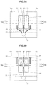
- FIG. 1 is a top view of a light emitting device according to a first embodiment.
- FIG. 2 is a vertical cross-sectional view of the light emitting device taken along section line A-A of FIG. 1 .
- FIGS. 3A and 3B are enlarged top views around one light emitting element included in the light emitting device according to the first embodiment.
- FIGS. 4A and 4B are top views showing modifications to an n-pad electrode and a p-pad electrode according to the first embodiment.
- FIGS. 5A and 5B are top views showing other modifications to the n-pad electrode and the p-pad electrode according to the first embodiment.
- FIG. 6 is a top view of a light emitting device according to a second embodiment.
- FIG. 7 is an enlarged top view around one light emitting element included in the light emitting device according to the second embodiment.
- FIG. 1 is a top view of a light emitting device 1 according to the first embodiment.
- FIG. 2 is a vertical cross-sectional view of the light emitting device 1 taken along section line A-A of FIG. 1 . Note that in FIG. 1 , underfill 16 and sealing resin 17 are not shown.
- the light emitting device 1 includes a wiring substrate 10 with electrodes 12 wired on a surface of a substrate 11 , and light emitting elements 20 connected to the electrodes 12 of the wiring substrate 10 .
- the substrate 11 is configured as, for example, a ceramic substrate such as an Al 2 O 3 substrate or an AlN substrate, a metal substrate such as an Al substrate or a Cu substrate whose surface is covered with an insulating film, or a glass epoxy substrate, and the electrodes 12 are made of an electrical conducting material such as copper.
- the electrodes 12 act as an n-electrode or a p-electrode to supply a current to the light emitting elements 20 . That is, one of the two electrodes 12 connected to each of the light emitting elements 20 acts as the n-electrode, and the other of the two electrodes 12 acts as the p-electrode.
- Each of the light emitting elements 20 is installed across a groove 30 between adjacent electrodes 12 on the wiring substrate 10 , that is, the gap 30 between the p-electrode and the n-electrode. For this reason, the gap 30 runs under each of the light emitting elements 20 .
- the pattern of the electrodes 12 is not limited to those shown in FIGS. 1 and 2 , and that the number and arrangement of the light emitting elements 20 are not limited to those shown in FIGS. 1 and 2 .
- the light emitting elements 20 are configured as, for example, LED chips having a chip substrate and a crystal layer including a light emitting layer and a cladding layer with the light emitting layer between it and the chip substrate.
- the light emitting elements 20 are being mounted with their crystal layers oriented toward the wiring substrate 10 side, that is, the light emitting elements 20 are being face-down mounted.
- the chip substrates are configured as transparent substrates made of sapphire or the like, and light is to be extracted from the chip substrate side. Further, the light emitting elements 20 may be configured as light emitting elements other than the LED chips, such as laser diodes or the like.
- the light emitting elements 20 include an n-pad electrode 14 n , which is joined directly to the n-electrodes (electrodes 12 ) without using an electrical conducting joining member such as an electrical conducting bump or an electrical conducting paste, and a p-pad electrode 14 p , which is joined directly to the p-electrodes (electrodes 12 ) without using an electrical conducting joining member.
- the n-pad electrodes 14 n and the p-pad electrodes 14 p are configured as the pad electrodes made of, for example, AuSn, and are joined to the electrodes 12 by heat treatment while being in contact with the electrodes 12 whose outermost surfaces are made of Au to diffuse Sn.
- FIGS. 3A and 3B are enlarged top views around one light emitting element 20 included in the light emitting device 1 , and show a configuration of the n-pad electrode 14 n and the p-pad electrode 14 p . Further, FIGS. 3A and 3B schematically show flow paths of an underfill 16 . The flow paths of the underfill 16 will be described later.
- n-electrode 12 n and p-electrode 12 p two of the electrodes 12 to which the one light emitting element 20 is connected are referred to as n-electrode 12 n and p-electrode 12 p , respectively.
- the outline of the one light emitting element 20 is indicated by a dotted line, and only the n-pad electrode 14 n and the p-pad electrode 14 p are indicated by a solid line.
- the adjacent other light emitting elements 20 , the electrodes 12 other than the n-electrode 12 n and the p-electrode 12 p , and a phosphor plate 21 are not shown.
- the n-pad electrode 14 n is being divided into an island 141 n and an island 142 n with a linear shape gap G 1 therebetween, while the p-pad electrode 14 p is being divided into an island 141 p and an island 142 p with a linear shape gap G 2 therebetween.
- the gap G 1 and the gap G 2 are continuous with a linear shape gap G 3 between the n-pad electrode 14 n and the p-pad electrode 14 p.
- FIGS. 3A and 3B Typical locations of the gap G 1 and the gap G 2 are shown in FIGS. 3A and 3B .
- a junction point of the gap G 1 with the gap G 3 and a junction point of the gap G 2 with the gap G 3 are located at a middle point of the gap G 3 in a length direction of the gap G 3 .
- the length directions of the gap G 1 and the gap G 2 are at right angles to the length direction of the gap G 3 .
- the underfill 16 is configured to fill a space between the wiring substrate 10 and the light emitting element 20 , to cover the n-pad electrode 14 n and the p-pad electrode 14 p of the light emitting element 20 , to be able to prevent exposure of the n-pad electrode 14 n and the p-pad electrode 14 p to moisture or air and damage (corrosion damage etc.) resulting therefrom. Further, the underfill 16 can also enhance the joining strength between the wiring substrate 10 and the light emitting element 20 . The fluid underfill 16 hardens after filling the space between the wiring substrate 10 and the light emitting element 20 .
- the underfill 16 is made of, for example, a resin such as a silicone based resin or an epoxy based resin.
- the underfill 16 acts as a reflecting material by including a white filler or the like therein, to be able to enhance the emission intensity of the light emitting device 1 .
- the fluid underfill 16 is dripped on the wiring substrate 10 with a dispenser or the like, and when the fluid underfill 16 comes into contact with an end portion of the gap 30 on the wiring substrate 10 , the fluid underfill 16 flows toward the light emitting element 20 due to capillary action in the gap 30 .
- the flow of the underfill 16 dripped to a dripping position 31 shown in FIGS. 3A and 3B will be described below as one example.
- the dripped underfill 16 flows through the dripping position 31 and mainly along three paths indicated by arrows in FIG. 3A .
- the path P 1 denotes the path through a space constituted by the gap 30 and the gap G 3 .
- the path P 2 denotes the path through a region on the n-electrode 12 n with the n-pad electrode 14 n being located between it and the gap G 3 .
- the path P 3 denotes the path through a region on the p-electrode 12 p with the p-pad electrode 14 p being located between it and the gap G 3 . That is, the path P 2 and the path P 3 denote the paths through the outer sides of the space between the wiring substrate 10 and the light emitting element 20 .
- the underfill 16 properly fills the space between the wiring substrate 10 and the light emitting element 20 .
- the gap G 1 and the gap G 2 serve as air escape routes to push out the air sandwiched between the underfills 16 within the space between the wiring substrate 10 and the light emitting element 20 to the outside via the gap G 1 and the gap G 2 , as indicated by arrows E 1 and E 2 of in FIG. 3B .
- the air is prevented from remaining in the underfill 16 as voids.
- the underfill 16 fills the space constituted by the gap 30 and the gap G 3 , and then flows from the gap G 3 side into the gap G 1 and the gap G 2 , and fills the gap G 1 and the gap G 2 . This makes it possible to fill the space between the wiring substrate 10 and the light emitting element 20 with the underfill 16 , while suppressing void formation in the underfill 16 .
- the thicknesses of the electrodes 12 are preferably 1.0 ⁇ m or more.
- FIG. 4A and FIG. 4B are top views corresponding to FIGS. 3A and 3B and showing modifications to the n-pad electrode 14 n and the p-pad electrode 14 p.
- the junction point of the gap G 1 with the gap G 3 and the junction point of the gap G 2 with the gap G 3 are located at a longer distance from the underfill 16 dripping position 31 on the wiring substrate 10 than the distance from the dripping position 31 to the middle point of the gap G 3 in the length direction of the gap G 3 .
- the distances from the dripping position 31 to the points where the underfill 16 entering through the path P 1 and the underfills 16 entering through the path P 2 or the path P 3 meet are often longer than the distance from the dripping position 31 to the middle point of the gap G 3 in the length direction of the gap G 3 , in which case it is possible to effectively allow the air to escape from the gap G 2 and the gap G 3 .
- the width of the gap G 3 is wider toward an outer side in a part of an underfill 16 dripping position 31 side region of the gap G 3 . This facilitates the forward movement of the underfill 16 to the path P 1 , while relatively reducing the amount of the underfill 16 which moves to the path P 2 and the path P 3 , therefore making it possible to more effectively suppress void formation in the underfill 16 to fill the space between the wiring substrate 10 and the light emitting element 20 .
- FIGS. 5A and 5B are top views corresponding to FIG. 3 and showing other modifications to the n-pad electrode 14 n and the p-pad electrode 14 p.
- the gap G 1 and the gap G 2 are inclined with respect to the gap G 3 in such a manner that the extending directions of the gap G 1 and the gap G 2 which are being extended toward the path P 2 and the path P 3 in the length directions of the gap G 1 and the gap G 2 intersect the forward movement directions of the path P 2 and the path P 3 at acute angles. For this reason, when the underfills 16 flowing through the path P 2 and the path P 3 are about to enter the gap G 1 and the gap G 2 from outer sides, the underfills 16 are required to bend their forward movement directions at the acute angles.
- the widths of the opposite (outer) end portions of the gap G 1 and the gap G 2 relative to the G 3 sides are smaller than the widths of the G 3 side end portions of the gap G 1 and the gap G 2 . This makes it possible to effectively slow the ingress of the underfills 16 passing through the path P 2 and the path P 3 into the gap G 1 and the gap G 2 from the outer sides.
- the widths of the gap G 1 and the gap G 2 are continuously changed in the length direction of the gap G 1 and the gap G 2 , but may be changed stepwise.
- a phosphor plate 21 is installed on the light emitting element 20 .
- the phosphor plate 21 is formed of a flat plate-like phosphor-containing member or a flat plate-like transparent member such as a flat plate-like resin member with a phosphor, for example, phosphor particles dispersed therein or a flat plate-like phosphor sintered body.
- the fluorescent color of the phosphor contained in the phosphor plate 21 or constituting the phosphor plate 21 is not particularly limited.
- the light emitting element 20 acts as an excitation light source for the phosphor contained in the phosphor plate 21 or constituting the phosphor plate 21 , and an emission color of the light emitting element 20 and an emission color of the phosphor plate 21 are mixed together to produce an emission color of the light emitting device 1 .
- the emission color of the light emitting element 20 is blue and the emission color of the phosphor plate 21 is yellow, the emission color of the light emitting device 1 is white.
- the light emitting device 1 may have a Zener diode 22 , which is electrically connected to the light emitting elements 20 to absorb a surge voltage, as shown in FIG. 1 .
- the installation position for the Zener diode 22 be out of the extended line of the gap 30 in order to prevent the Zener diode 22 from obstructing the dripping of the underfill 16 , or the dripped underfill 16 from being attracted to the Zener diode 22 side.
- the light emitting device 1 may have an annular dam 13 , which is formed in such a manner as to surround the installation region for the light emitting elements 20 .
- the dam 13 is made of, for example, a resin such as a silicone based resin or an epoxy based resin, and may contain a white dye such as titanium oxide.
- the region in the inner side of the dam 13 is filled with a sealing resin 17 for sealing the light emitting elements 20 .
- the sealing resin 17 is made of, for example, a transparent resin such as a silicone based resin or an epoxy based resin.
- the sealing resin 17 may contain a phosphor.
- a light emitting device has, on electrodes 12 , flow blocking portions to suppress the flows of the unhardened underfills 16 flowing through the outer sides of the light emitting elements 20 .
- flow blocking portions to suppress the flows of the unhardened underfills 16 flowing through the outer sides of the light emitting elements 20 .
- FIG. 6 is a top view of the light emitting device 2 according to the second embodiment.
- FIG. 7 is an enlarged top view around one light emitting element 20 included in the light emitting device 2 before completion of filling with the underfill 16 .
- FIG. 7 in the same manner as in FIG. 3 , the outline of the one light emitting element 20 is indicated by a dotted line, and only the n-pad electrode 14 n and the p-pad electrode 14 p are indicated by a solid line. Further, the adjacent other light emitting elements 20 , the electrodes 12 other than the n-electrode 12 n and the p-electrode 12 p , and the phosphor plate 21 are not shown.
- the flow blocking portions 15 are being provided at positions in the outer sides of the space between the wiring substrate 10 and the light emitting elements 20 , in other words, at such a position on the n-electrode 12 n that the n-pad electrode 14 n is located between the n-electrode 12 n and the gap G 3 , and at such a position on the p-electrode 12 p that the p-pad electrode 14 p is located between the p-electrode 12 p and the gap G 3 .
- the flow blocking portions 15 are configured as holes or protrusions provided on the electrodes 12 (the n-electrode 12 n and the p-electrode 12 p ).
- the flow blocking portions 15 when configured as holes may be configured as through holes, which pass through the electrodes 12 or may be configured as recesses of the electrodes 12 , which do not pass through the electrodes 12 .
- the flow blocking portions 15 when configured as protrusions may be configured as part of the electrodes 12 or may separately be installed on the surfaces of the electrodes 12 .
- the flow blocking portions 15 are being provided on the path P 2 and the path P 3 of the underfill 16 , the flow blocking portions 15 are able to block the flows of the underfills 16 flowing through the path P 2 and the path P 3 . This makes it possible to relatively increase the flow speed of the underfill 16 flowing in the path P 1 , and thereby suppress void formation in the underfill 16 resulting from the ingress of the underfill 16 into the space constituted by the gap 30 and the gap G 3 from both the sides.
- the light emitting device 2 has the gap G 1 and the gap G 2 , to make it possible to effectively allow the air in the space between the wiring substrate 10 and the light emitting element 20 to escape to the outside, and therefore more effectively suppress void formation in the underfill 16 to fill the space between the wiring substrate 10 and the light emitting element 20 .
- the flow blocking portions 15 block the flows of the underfills 16 flowing through the path P 2 and the path P 3 , the underfill 16 hardens while remaining in contact with the flow blocking portions 15 .
- the light emitting device 1 by providing the gap G 1 and the gap G 2 , it is possible to suppress void formation in the underfill 16 in the space between the wiring substrate 10 and the light emitting elements 20 .
- the light emitting device 1 by providing the flow blocking portions 15 , it is possible to more effectively suppress void formation in the underfill 16 in the space between the wiring substrate 10 and the light emitting elements 20 .
- the light emitting device 1 and the light emitting device 2 have their structures to be able to suppress void formation in the underfill 16 in the space between the wiring substrate 10 and the light emitting elements 20 , even when the underfill 16 and the sealing resin 17 are continuously integrally formed of the same material, void formation therein is likely to be able to be sufficiently suppressed.
- the resin is poured evenly into the region between the dam 13 and the light emitting elements 20 to form the underfill 16 and the sealing resin 17 .
- the light emitting device 1 and the light emitting device 2 may have only one of the gap G 1 and the gap G 2 as long as the void formation in the underfill 16 in the space between the wiring substrate 10 and the light emitting elements 20 can be suppressed. That is, only one of the n-pad electrode 14 n and the p-pad electrode 14 p may be divided.
Landscapes
- Led Device Packages (AREA)
- Engineering & Computer Science (AREA)
- Power Engineering (AREA)
- Microelectronics & Electronic Packaging (AREA)
- Physics & Mathematics (AREA)
- Condensed Matter Physics & Semiconductors (AREA)
- General Physics & Mathematics (AREA)
- Computer Hardware Design (AREA)
Abstract
Description
[2] The light emitting device according to [1] above, further including flow blocking portions, which are provided at such a position on the n-electrode that the n-pad electrode is located between the n-electrode and the third gap, and at such a position on the p-electrode that the p-pad electrode is located between the p-electrode and the third gap, to block flow of the underfill before hardening of the underfill by contact with the underfill.
[3] The light emitting device according to the above [1] or [2], wherein a junction point of the second gap with the third gap is shifted from a middle point of the third gap in a length direction of the third gap.
[4] The light emitting device according to any one of the above [1] to [3], wherein in a part of a region of the third gap including one end portion in a length direction of the third gap, the third gap is wider in width towards that one end portion.
[5] The light emitting device according to any one of the above [1] to [4], wherein the n-electrode and the p-electrode are 1.0 μm or more in thickness.
[6] A light emitting device, comprising: a wiring substrate including an n-electrode and a p-electrode formed on a surface thereof; a light emitting element provided on the n-electrode and the p-electrode, the light emitting element including an n-pad electrode and a p-pad electrode that are connected to the n-electrode and the p-electrode of the wiring substrate; an underfill that fills a space between the wiring substrate and the light emitting element; and a gap for suppressing void formation in the underfill filled in the space.
[7] The light emitting device according to the above [6], wherein the gap comprises: a first gap that is formed between the n- and p-electrodes; a second gap that is formed on an edge on a side of the n-pad electrode and another edge on an opposite side of the n-pad electrode; and a third gap that is formed on an edge on a side of the p-pad electrode and another edge on an opposite side of the p-pad electrode.
- 1, 2 Light emitting device
- 10 Wiring substrate
- 11 Substrate
- 12, 12 n, 12 p-electrode
- 13 Dam
- 14 n n-pad electrode
- 141 n, 142 n Island
- 14 p p-pad electrode
- 141 p, 142 p Island
- 15 Flow blocking portion
- 16 Underfill
- 17 Sealing resin
- 20 Light emitting element
- 30 Gap
- G1, G2, G3 Gap
Claims (19)
Applications Claiming Priority (3)
| Application Number | Priority Date | Filing Date | Title |
|---|---|---|---|
| JPJP2018-184318 | 2018-09-28 | ||
| JP2018184318A JP7021625B2 (en) | 2018-09-28 | 2018-09-28 | Luminescent device |
| JP2018-184318 | 2018-09-28 |
Publications (2)
| Publication Number | Publication Date |
|---|---|
| US20200105985A1 US20200105985A1 (en) | 2020-04-02 |
| US11088303B2 true US11088303B2 (en) | 2021-08-10 |
Family
ID=69946152
Family Applications (1)
| Application Number | Title | Priority Date | Filing Date |
|---|---|---|---|
| US16/534,583 Active US11088303B2 (en) | 2018-09-28 | 2019-08-07 | Light emitting device |
Country Status (3)
| Country | Link |
|---|---|
| US (1) | US11088303B2 (en) |
| JP (1) | JP7021625B2 (en) |
| CN (1) | CN110970536B (en) |
Citations (5)
| Publication number | Priority date | Publication date | Assignee | Title |
|---|---|---|---|---|
| US20090101929A1 (en) * | 2007-10-22 | 2009-04-23 | Philips Lumileds Lighting Company, Llc | Robust led structure for substrate lift-off |
| US20110297994A1 (en) * | 2010-06-03 | 2011-12-08 | Kabushiki Kaisha Toshiba | Semiconductor light emitting device |
| US20110303894A1 (en) * | 2010-06-09 | 2011-12-15 | Nichia Corporation | Semiconductor light emitting element and fabricating method |
| US20160035952A1 (en) * | 2010-02-09 | 2016-02-04 | Nichia Corporation | Light emitting device and method for manufacturing light emitting device |
| JP2018019032A (en) | 2016-07-29 | 2018-02-01 | 豊田合成株式会社 | Method for manufacturing light emitting device |
Family Cites Families (10)
| Publication number | Priority date | Publication date | Assignee | Title |
|---|---|---|---|---|
| JP2571024B2 (en) * | 1994-09-28 | 1997-01-16 | 日本電気株式会社 | Multi-chip module |
| JP3431406B2 (en) * | 1996-07-30 | 2003-07-28 | 株式会社東芝 | Semiconductor package equipment |
| JP4580633B2 (en) * | 2003-11-14 | 2010-11-17 | スタンレー電気株式会社 | Semiconductor device and manufacturing method thereof |
| US7902678B2 (en) * | 2004-03-29 | 2011-03-08 | Nec Corporation | Semiconductor device and manufacturing method thereof |
| JP4536603B2 (en) * | 2005-06-09 | 2010-09-01 | 新光電気工業株式会社 | Manufacturing method of semiconductor device, mounting substrate for semiconductor device, and semiconductor device |
| WO2011148615A1 (en) * | 2010-05-26 | 2011-12-01 | 株式会社村田製作所 | Substrate with built-in component |
| JP2012079876A (en) * | 2010-09-30 | 2012-04-19 | Fujitsu Ltd | Method of manufacturing electronic device, and electronic device |
| EP2439793B1 (en) * | 2010-10-11 | 2016-03-16 | LG Innotek Co., Ltd. | Light emitting device and lighting instrument including the same |
| KR102212666B1 (en) * | 2014-06-27 | 2021-02-05 | 엘지이노텍 주식회사 | Light emitting device |
| EP3561870A4 (en) * | 2016-12-23 | 2020-11-25 | Lumens Co., Ltd. | MICRO LED MODULE AND MANUFACTURING PROCESS FOR IT |
-
2018
- 2018-09-28 JP JP2018184318A patent/JP7021625B2/en active Active
-
2019
- 2019-08-07 US US16/534,583 patent/US11088303B2/en active Active
- 2019-08-28 CN CN201910801537.0A patent/CN110970536B/en active Active
Patent Citations (6)
| Publication number | Priority date | Publication date | Assignee | Title |
|---|---|---|---|---|
| US20090101929A1 (en) * | 2007-10-22 | 2009-04-23 | Philips Lumileds Lighting Company, Llc | Robust led structure for substrate lift-off |
| US20160035952A1 (en) * | 2010-02-09 | 2016-02-04 | Nichia Corporation | Light emitting device and method for manufacturing light emitting device |
| US20110297994A1 (en) * | 2010-06-03 | 2011-12-08 | Kabushiki Kaisha Toshiba | Semiconductor light emitting device |
| US20110303894A1 (en) * | 2010-06-09 | 2011-12-15 | Nichia Corporation | Semiconductor light emitting element and fabricating method |
| JP2018019032A (en) | 2016-07-29 | 2018-02-01 | 豊田合成株式会社 | Method for manufacturing light emitting device |
| US20180033926A1 (en) | 2016-07-29 | 2018-02-01 | Toyoda Gosei Co., Ltd. | Method of manufacturing light-emitting device |
Also Published As
| Publication number | Publication date |
|---|---|
| CN110970536A (en) | 2020-04-07 |
| CN110970536B (en) | 2023-06-09 |
| US20200105985A1 (en) | 2020-04-02 |
| JP2020053644A (en) | 2020-04-02 |
| JP7021625B2 (en) | 2022-02-17 |
Similar Documents
| Publication | Publication Date | Title |
|---|---|---|
| US10892393B2 (en) | Light emitting device having external connection with different width | |
| US12080695B2 (en) | Method for manufacturing light emitting devices | |
| CN104300068B (en) | Light emitting device and manufacturing method thereof | |
| TWI738203B (en) | Light emitting device | |
| JP6699432B2 (en) | Method for manufacturing light emitting device | |
| US9960333B2 (en) | Light-emitting device including light-emitting elements connected in series and light-emitting elements connected in parallel | |
| JP6318495B2 (en) | Light emitting device | |
| US11088303B2 (en) | Light emitting device | |
| CN107534076B (en) | LED package, light-emitting device, and manufacturing method of LED package | |
| JP2025024978A (en) | Light-emitting device | |
| JP2019029459A (en) | Light emitting device and manufacturing method thereof |
Legal Events
| Date | Code | Title | Description |
|---|---|---|---|
| FEPP | Fee payment procedure |
Free format text: ENTITY STATUS SET TO UNDISCOUNTED (ORIGINAL EVENT CODE: BIG.); ENTITY STATUS OF PATENT OWNER: LARGE ENTITY |
|
| AS | Assignment |
Owner name: TOYODA GOSEI CO., LTD., JAPAN Free format text: ASSIGNMENT OF ASSIGNORS INTEREST;ASSIGNORS:SENGOKU, AKIRA;ITO, SHUN;REEL/FRAME:050122/0562 Effective date: 20190730 |
|
| STPP | Information on status: patent application and granting procedure in general |
Free format text: NON FINAL ACTION MAILED |
|
| STPP | Information on status: patent application and granting procedure in general |
Free format text: RESPONSE TO NON-FINAL OFFICE ACTION ENTERED AND FORWARDED TO EXAMINER |
|
| STPP | Information on status: patent application and granting procedure in general |
Free format text: NOTICE OF ALLOWANCE MAILED -- APPLICATION RECEIVED IN OFFICE OF PUBLICATIONS |
|
| STPP | Information on status: patent application and granting procedure in general |
Free format text: PUBLICATIONS -- ISSUE FEE PAYMENT VERIFIED |
|
| STCF | Information on status: patent grant |
Free format text: PATENTED CASE |
|
| MAFP | Maintenance fee payment |
Free format text: PAYMENT OF MAINTENANCE FEE, 4TH YEAR, LARGE ENTITY (ORIGINAL EVENT CODE: M1551); ENTITY STATUS OF PATENT OWNER: LARGE ENTITY Year of fee payment: 4 |