US11085127B2 - Methods of introducing dopant into a melt of semiconductor or solar-grade material via a feed tube - Google Patents
Methods of introducing dopant into a melt of semiconductor or solar-grade material via a feed tube Download PDFInfo
- Publication number
- US11085127B2 US11085127B2 US16/235,677 US201816235677A US11085127B2 US 11085127 B2 US11085127 B2 US 11085127B2 US 201816235677 A US201816235677 A US 201816235677A US 11085127 B2 US11085127 B2 US 11085127B2
- Authority
- US
- United States
- Prior art keywords
- dopant
- melt
- feed tube
- introducing
- outlet
- Prior art date
- Legal status (The legal status is an assumption and is not a legal conclusion. Google has not performed a legal analysis and makes no representation as to the accuracy of the status listed.)
- Active, expires
Links
- 239000002019 doping agent Substances 0.000 title claims abstract description 194
- 239000000155 melt Substances 0.000 title claims abstract description 97
- 238000000034 method Methods 0.000 title claims abstract description 45
- 239000000463 material Substances 0.000 title claims abstract description 39
- 239000004065 semiconductor Substances 0.000 title claims abstract description 23
- 239000007787 solid Substances 0.000 claims abstract description 50
- 239000013078 crystal Substances 0.000 claims abstract description 44
- 239000007788 liquid Substances 0.000 claims abstract description 32
- 230000008018 melting Effects 0.000 claims abstract description 13
- 238000002844 melting Methods 0.000 claims abstract description 13
- XUIMIQQOPSSXEZ-UHFFFAOYSA-N Silicon Chemical group [Si] XUIMIQQOPSSXEZ-UHFFFAOYSA-N 0.000 claims description 7
- 229910052710 silicon Inorganic materials 0.000 claims description 7
- 239000010703 silicon Substances 0.000 claims description 7
- 229910052787 antimony Inorganic materials 0.000 claims description 4
- WATWJIUSRGPENY-UHFFFAOYSA-N antimony atom Chemical compound [Sb] WATWJIUSRGPENY-UHFFFAOYSA-N 0.000 claims description 4
- 229910052738 indium Inorganic materials 0.000 claims description 4
- APFVFJFRJDLVQX-UHFFFAOYSA-N indium atom Chemical compound [In] APFVFJFRJDLVQX-UHFFFAOYSA-N 0.000 claims description 4
- GYHNNYVSQQEPJS-UHFFFAOYSA-N Gallium Chemical compound [Ga] GYHNNYVSQQEPJS-UHFFFAOYSA-N 0.000 claims description 3
- 229910052782 aluminium Inorganic materials 0.000 claims description 3
- XAGFODPZIPBFFR-UHFFFAOYSA-N aluminium Chemical compound [Al] XAGFODPZIPBFFR-UHFFFAOYSA-N 0.000 claims description 3
- 229910052733 gallium Inorganic materials 0.000 claims description 3
- 229910052716 thallium Inorganic materials 0.000 claims description 3
- BKVIYDNLLOSFOA-UHFFFAOYSA-N thallium Chemical compound [Tl] BKVIYDNLLOSFOA-UHFFFAOYSA-N 0.000 claims description 3
- 230000007246 mechanism Effects 0.000 description 8
- 239000010453 quartz Substances 0.000 description 6
- VYPSYNLAJGMNEJ-UHFFFAOYSA-N silicon dioxide Inorganic materials O=[Si]=O VYPSYNLAJGMNEJ-UHFFFAOYSA-N 0.000 description 6
- 238000010438 heat treatment Methods 0.000 description 5
- 230000008878 coupling Effects 0.000 description 3
- 238000010168 coupling process Methods 0.000 description 3
- 238000005859 coupling reaction Methods 0.000 description 3
- 230000007547 defect Effects 0.000 description 3
- 238000007667 floating Methods 0.000 description 3
- 239000000289 melt material Substances 0.000 description 3
- 239000002245 particle Substances 0.000 description 3
- 229910021420 polycrystalline silicon Inorganic materials 0.000 description 3
- 230000035939 shock Effects 0.000 description 3
- 238000011109 contamination Methods 0.000 description 2
- 230000008020 evaporation Effects 0.000 description 2
- 238000001704 evaporation Methods 0.000 description 2
- 239000011819 refractory material Substances 0.000 description 2
- 230000000717 retained effect Effects 0.000 description 2
- 229910001220 stainless steel Inorganic materials 0.000 description 2
- 239000010935 stainless steel Substances 0.000 description 2
- 230000015572 biosynthetic process Effects 0.000 description 1
- 238000004891 communication Methods 0.000 description 1
- 150000001875 compounds Chemical class 0.000 description 1
- 238000010276 construction Methods 0.000 description 1
- 230000008014 freezing Effects 0.000 description 1
- 238000007710 freezing Methods 0.000 description 1
- 239000008187 granular material Substances 0.000 description 1
- 230000002401 inhibitory effect Effects 0.000 description 1
- 229910021421 monocrystalline silicon Inorganic materials 0.000 description 1
- 229920005591 polysilicon Polymers 0.000 description 1
- 238000002360 preparation method Methods 0.000 description 1
- 239000007858 starting material Substances 0.000 description 1
Images


Classifications
-
- C—CHEMISTRY; METALLURGY
- C30—CRYSTAL GROWTH
- C30B—SINGLE-CRYSTAL GROWTH; UNIDIRECTIONAL SOLIDIFICATION OF EUTECTIC MATERIAL OR UNIDIRECTIONAL DEMIXING OF EUTECTOID MATERIAL; REFINING BY ZONE-MELTING OF MATERIAL; PRODUCTION OF A HOMOGENEOUS POLYCRYSTALLINE MATERIAL WITH DEFINED STRUCTURE; SINGLE CRYSTALS OR HOMOGENEOUS POLYCRYSTALLINE MATERIAL WITH DEFINED STRUCTURE; AFTER-TREATMENT OF SINGLE CRYSTALS OR A HOMOGENEOUS POLYCRYSTALLINE MATERIAL WITH DEFINED STRUCTURE; APPARATUS THEREFOR
- C30B15/00—Single-crystal growth by pulling from a melt, e.g. Czochralski method
- C30B15/02—Single-crystal growth by pulling from a melt, e.g. Czochralski method adding crystallising materials or reactants forming it in situ to the melt
- C30B15/04—Single-crystal growth by pulling from a melt, e.g. Czochralski method adding crystallising materials or reactants forming it in situ to the melt adding doping materials, e.g. for n-p-junction
-
- C—CHEMISTRY; METALLURGY
- C30—CRYSTAL GROWTH
- C30B—SINGLE-CRYSTAL GROWTH; UNIDIRECTIONAL SOLIDIFICATION OF EUTECTIC MATERIAL OR UNIDIRECTIONAL DEMIXING OF EUTECTOID MATERIAL; REFINING BY ZONE-MELTING OF MATERIAL; PRODUCTION OF A HOMOGENEOUS POLYCRYSTALLINE MATERIAL WITH DEFINED STRUCTURE; SINGLE CRYSTALS OR HOMOGENEOUS POLYCRYSTALLINE MATERIAL WITH DEFINED STRUCTURE; AFTER-TREATMENT OF SINGLE CRYSTALS OR A HOMOGENEOUS POLYCRYSTALLINE MATERIAL WITH DEFINED STRUCTURE; APPARATUS THEREFOR
- C30B29/00—Single crystals or homogeneous polycrystalline material with defined structure characterised by the material or by their shape
- C30B29/02—Elements
- C30B29/06—Silicon
Definitions
- the field relates generally to preparation of single crystals of semiconductor or solar-grade material and, more specifically, to a liquid doping system for controlled doping of a melt of semiconductor or solar-grade material.
- Single crystal material which is the starting material for fabricating many electronic components such as semiconductor devices and solar cells, is commonly prepared using the Czochralski (“CZ”) method.
- CZ Czochralski
- the Czochralski method involves melting polycrystalline source material, such as polycrystalline silicon (“polysilicon”), in a crucible to form a silicon melt and then pulling a single-crystal ingot from the melt.
- polycrystalline source material such as polycrystalline silicon (“polysilicon”)
- dopants are added to the molten source material to modify the base resistivity of the resulting monocrystalline structure.
- Dopants are often added to the molten source material in solid form, at least for p-type and n-type silicon.
- solid dopants presents several drawbacks.
- One drawback is a thermal shock resulting from the temperature difference between solid dopants and the molten source material. This thermal shock causes the molten source material to solidify underneath the solid dopant granules, creating “floating boats”. Additionally, quartz particles can form during the formation of the floating boats. These quartz particles may remain in the molten source material long after the floating boats have melted, resulting in crystal defects or loss of crystal structure.
- a further drawback resulting from the addition of solid dopants to the molten source material is contamination of the monocrystalline growing assembly.
- the impact of solid dopants on the surface of the molten source material causes the molten source material to splash out of the crucible and onto various components of the monocrystalline growing assembly, which may result in crystal defects or damage to components in the assembly.
- a method of growing a doped monocrystalline ingot using a crystal growing system includes a growth chamber, a dopant feeding device, and a feed tube.
- the method includes preparing a melt of semiconductor or solar-grade material in a crucible disposed within the growth chamber, introducing a solid dopant into the feed tube with the dopant feeding device, melting the solid dopant within the feed tube to a form a liquid dopant, introducing the liquid dopant into the melt below a surface of the melt, and growing a monocrystalline ingot from the melt by contacting the melt with a seed crystal and pulling the seed crystal away from the melt.
- a method of introducing a dopant into a melt of semiconductor or solar-grade material using a feed tube and a dopant feeding device includes introducing a solid dopant into the feed tube with the dopant feeding device, melting the solid dopant within the feed tube to a form a liquid dopant, and introducing the liquid dopant into the melt below a surface of the melt.
- a system for growing a single crystal ingot from a melt of semiconductor or solar-grade material includes a housing defining a crystal growth chamber, a crucible disposed within the growth chamber for holding a melt of semiconductor or solar-grade material, a dopant feeding device configured to dispense solid dopant, and a feed tube.
- the feed tube is configured to receive solid dopant from the dopant feeding device and dispense liquid dopant into the melt.
- the feed tube defines a dopant outlet, and includes a restrictor nozzle configured to inhibit solid dopant from passing through the dopant outlet and to allow liquid dopant to pass through the dopant outlet.
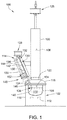
- FIG. 1 is a cross-section of a crystal growing system including an example doping system for introducing liquid dopant into a melt;
- FIG. 2 is a cross-section of a dopant feeding device suitable for use with the doping system of FIG. 1 ;
- FIG. 3 is an enlarged cross-sectional view of a feed tube of the doping system of FIG. 1 ;
- FIG. 4 is a flow chart of an example method of growing a doped monocrystalline ingot using the crystal growing system of FIG. 1 .
- a crystal growing system is shown schematically and is indicated generally at 100 in FIG. 1 .
- the crystal growing system 100 is used to produce monocrystalline (i.e., single crystal) ingots of semiconductor or solar-grade material (e.g., silicon) by the Czochralski (CZ) method.
- CZ Czochralski
- the crystal growing system 100 is described herein with reference to a batch or recharge CZ method, the crystal growing system 100 may also be used to grow monocrystalline ingots by a continuous CZ method.
- the illustrated crystal growing system 100 generally includes a housing 102 defining a growth chamber 104 and an ingot removal chamber 106 connected to and positioned above the growth chamber 104 .
- a crucible 108 containing a melt 110 of semiconductor or solar-grade material e.g., silicon
- one or more heating elements 112 are positioned proximate the crucible 108 for supplying thermal energy to the system 100 .
- the crystal growing system 100 also includes an automatic doping system 114 connected to the housing 102 for introducing dopant into the melt 110 .
- the housing 102 includes a lower portion 116 , an upper dome 118 connected to the lower portion 116 , and an elongate tubular portion 120 extending generally upward from the upper dome 118 .
- the growth chamber 104 is defined by the lower portion 116 and the upper dome 118
- the ingot removal chamber 106 is generally defined by the elongate tubular portion 120 .
- the upper dome 118 includes a central annular opening 122 providing communication between the growth chamber 104 and the removal chamber 106 , and a feed port 124 (broadly, an opening) through which dopants may be introduced into the melt 110 .
- the feed port 124 is defined along the upper dome 118 , although the feed port 124 may be located along any suitable portion of the housing 102 that enables the doping system 114 to function as described herein.
- the housing 102 may be made of stainless steel or other suitable materials.
- one or more of the lower portion 116 , the upper dome 118 , and the tubular portion 120 may include water-cooled stainless steel walls.
- the crucible 108 is positioned within the growth chamber 104 and beneath the removal chamber 106 such that an ingot grown from the melt 110 can be pulled by a crystal pulling mechanism 126 through the central opening 122 in the upper dome 118 and into the removal chamber 106 .
- the crucible 108 may be supported within the growth chamber 104 by a susceptor (not shown) and a rotatable shaft (not shown) configured to rotate the crucible 108 during growth of a crystal ingot.
- the crucible 108 may be made of, for example, quartz or any other suitable material that enables the crystal growing system 100 to function as described herein. Further, the crucible 108 may have any suitable size that enables the crystal growing system 100 to function as described herein. In some embodiments, the crucible 108 has a diameter of between about 16 inches and about 32 inches, more suitably between about 20 inches and about 28 inches, and even more suitably between about 20 inches and about 24 inches. In other embodiments, the crucible 108 may have a diameter less than about 16 inches or greater than about 32 inches.
- the doping system 114 generally includes a dopant feeding device 128 and a feed tube 130 .
- the dopant feeding device 128 is secured to the housing 102 , and is positioned outside of the growth chamber 104 .
- the feed tube 130 is positioned proximate an outlet of the dopant feeding device 128 , and extends through the feed port 124 of the housing 102 and into the growth chamber 104 .
- the dopant feeding device 128 is configured to dispense solid dopant into the feed tube 130
- the feed tube 130 is configured to retain solid dopant therein until the dopant is melted, and to introduce liquid dopant into the melt 110 .
- FIG. 2 is a cross section of an example dopant feeding device 200 suitable for use with the doping system 114 of FIG. 1 .
- the example dopant feeding device 200 is configured to dispense metered quantities of solid dopant through an outlet 202 defined at the lowermost point of the dopant feeding device 200 .
- the dopant feeding device 200 generally includes a fill assembly 204 , a hopper 206 , and a double valve system 208 .
- the fill assembly 204 includes a fill port 210 and a feed tube 212 connected to the fill port 210 and extending from the fill port 210 into the hopper 206 .
- dopant is fed into the fill port 210 and is funneled down into the feed tube 212 and into the hopper 206 .
- the hopper 206 includes a dopant container 214 for storing dopant, and a dopant funnel 216 connected to a lower opening 218 of the dopant container 214 .
- Dopant fed into the fill port 210 is directed into the dopant container 214 by the feed tube 212 .
- Dopant is stored in the dopant container 214 , and is released in metered quantities into the dopant funnel 216 using the double valve system 208 .
- the double valve system 208 includes a lower valve 220 and an upper valve 222 .
- the lower valve 220 and the upper valve 222 are both operably connected to a pneumatic actuator 224 .
- a fill chamber 226 is defined between the upper valve 222 and the dopant container 214 .
- the volume of the chamber 226 defines the dopant charge or the amount of dopant released by the dopant feeding device 200 in a single discharge.
- the pneumatic actuator 224 is configured to vertically reciprocate the lower valve 220 and the upper valve 222 to release metered quantities of dopant from the chamber 226 into the dopant funnel 216 through the lower opening 218 of the dopant container 214 .
- Dopant released into the dopant funnel 216 is dispensed from the dopant feeding device 200 into the feed tube 212 through the outlet 202 defined at the lowermost point of dopant feeding device 200 .
- the dopant feeding device 200 is described in greater detail in International Patent Application No. PCT/IT2013/000161, which is hereby incorporated by reference in its entirety.
- the feed tube 130 includes a first end 132 , a second end 134 distal from the first end 132 , and an annular sidewall 136 extending along a longitudinal axis of the feed tube 130 from the first end 132 to second end 134 .
- the feed tube 130 has a dopant inlet 138 defined at the first end 132 , a dopant outlet 140 (also shown in FIG. 3 ) defined at the second end 134 , and a dopant passage 142 defined therein extending from the dopant inlet 138 to the dopant outlet 140 .
- Solid dopant dispensed from the dopant feeding device 128 is received in the feed tube 130 at the dopant inlet 138 , and falls through the dopant passage 142 towards the dopant outlet 140 where the solid dopant is retained until it is melted and released into the melt 110 .
- the feed tube 130 is a telescopic feed tube, including a fixed, inner feed tube 144 and moveable, outer feed tube 146 .
- the inner feed tube 144 is secured in a fixed relationship to one or both of the housing 102 and the dopant feeding device 128 , and the outer feed tube 146 is configured to move relative to the inner feed tube 144 .
- the inner feed tube 144 and the outer feed tube 146 are concentrically arranged about a common longitudinal axis, and the outer feed tube 146 is configured to move along the longitudinal axis between an extended position (shown in FIG. 1 ) and a retracted position (not shown in FIG. 1 ).
- the inner feed tube 144 defines the first end 132 and the dopant inlet 138 of the feed tube 130
- the outer feed tube 146 defines the second end 134 and the dopant outlet 140 of the feed tube 130 .
- the components of the feed tube 130 are suitably made of refractory materials that remain substantially chemically inert at elevated temperatures.
- Suitable materials from which the components of the feed tube 130 may be made of include, for example and without limitation, quartz.
- the outer feed tube 146 is operatively connected to a linear slide mechanism 148 configured to move the outer feed tube 146 between the extended position (shown in FIG. 1 ) and the retracted position (not shown in FIG. 1 ).
- the linear slide mechanism 148 is configured to retract the outer feed tube 146 entirely out of the growth chamber 104 when the outer feed tube 146 is in the retracted position.
- at least a portion of the outer feed tube 146 is positioned within the growth chamber 104 when the outer feed tube 146 is in the retracted position.
- the linear slide mechanism 148 may include any suitable device or combination of devices that enable the doping system 114 to function as described herein including, for example and without limitation, tracks, rails, rollers, bearing mechanisms, actuators, and combinations thereof.
- the linear slide mechanism 148 includes a rail 150 , coupling members 152 slidably connected to the rail 150 and attached to the outer feed tube 146 , and an actuator (not shown) operably connected to one or both of the outer feed tube 146 and the coupling members 152 .
- the actuator of the linear slide mechanism 148 is configured to move the coupling members 152 along the rail 150 , and move the outer feed tube 146 between the extended and retracted positions.
- linear actuating devices other than a linear slide mechanism may be used to move the outer feed tube 146 between the extended and retracted positions.
- FIG. 3 is an enlarged cross-sectional view of the feed tube 130 , specifically, the outer feed tube 146 .
- the dopant outlet 140 is submerged at a depth 302 below a surface 304 of the melt 110 .
- the outer feed tube 146 includes a restrictor nozzle 306 at the second end 134 of the feed tube 130 configured to inhibit solid dopant 308 from passing through the dopant outlet 140 and to allow liquid dopant to pass through the dopant outlet 140 .
- the restrictor nozzle 306 includes a conical portion 310 extending radially inward from the annular sidewall 136 to the dopant outlet 140 at an angle 312 , and defines a diameter 314 of the dopant outlet 140 sized to inhibit solid dopant 308 from passing therethrough.
- the dopant outlet 140 may have any suitable diameter 314 that enables the doping system 114 to function as described herein, and may vary depending on the type of solid dopant 308 used to dope the melt 110 . In some embodiments, for example, the dopant outlet 140 has a diameter of between about 1 millimeter (mm) and about 4 mm, and is configured to receive solid dopant 308 having an average particle size of between about 2 mm and about 5 mm.
- the angle 312 at which the conical portion 310 of the restrictor nozzle 306 extends inward from the sidewall 136 is between about 15° and about 35° and, more suitably, between about 20° and about 30°.
- the conical portion 310 extends inward from the sidewall 136 at an angle of about 25°.
- the conical portion 310 of the restrictor nozzle 306 extends inward from the sidewall 136 at an angle 312 such that, when the feed tube 130 is in the extended position, the conical portion 310 and the reminder of the restrictor nozzle 306 are generally oriented at the same angle with respect to the surface of the melt 110 , as shown in FIG. 3 .
- Solid dopant 308 introduced into the feed tube 130 is retained within the dopant passage 142 by the restrictor nozzle 306 at the second end 134 of the feed tube 130 until the solid dopant 308 is melted by heat from the melt 110 and/or the heating elements 112 .
- the liquid dopant flows out of the feed tube 130 through the dopant outlet 140 and into the melt 110 .
- the shape and orientation of restrictor nozzle 306 and, in particular, the angle 312 at which conical portion 310 extends from the sidewall 136 facilitate dispensing all liquid dopant from within the feed tube 130 .
- the restrictor nozzle 306 is also configured to inhibit liquid melt material from flowing upward into the feed tube 130 through the dopant outlet 140 , which can damage or impair operability of the feed tube 130 (e.g., by clogging the dopant outlet 140 ).
- the restrictor nozzle 306 is sized and shaped, and made of suitable materials so that the interfacial surface energy between the melt 110 and the restrictor nozzle 306 and the surface tension of the melt 110 inhibits melt material from flowing upward into the feed tube 130 through the dopant outlet 140 .
- the outer feed tube 146 is suitably made of quartz, and has a dopant outlet 140 with a diameter in the range of between about 1 mm and about 4 mm.
- the outer feed tube 146 is suitable for introducing liquid dopant into the melt 110 at a depth 302 up to about 5 mm.
- the outer feed tube 146 may be made of materials other than quartz, such as other refractory materials that remain inert at elevated temperatures, and have a dopant outlet with a diameter less than about 1 mm or greater than about 4 mm.
- the crystal growing system 100 is used to grow doped monocrystalline ingots, such as antimony-doped single crystal silicon ingots, from the melt 110 .
- the melt 110 is prepared in the crucible 108 by charging the crucible 108 with feedstock material, such as chunk polycrystalline silicon.
- the feedstock material is melted in the crucible 108 using heating elements 112 to form the melt 110 of semiconductor or solar grade material.
- Dopants are added the melt 110 using the automatic doping system 114 by dispensing solid dopant from the dopant feeding device 128 into the feed tube 130 , melting the solid dopant within the feed tube 130 to form liquid dopant, and introducing the liquid dopant into the melt 110 through the dopant outlet 140 at a depth below the surface of the melt 110 .
- a monocrystalline ingot is grown from the melt 110 by contacting the melt 110 with a seed crystal (not shown) to initiate crystal growth, and subsequently pulling the seed crystal away from the melt to grow the monocrystalline ingot.
- FIG. 4 is a flow chart of an example method 400 of growing a doped monocrystalline ingot using the crystal growing system 100 described above with reference to FIGS. 1-3 .
- the method 400 generally includes preparing 410 a melt of semiconductor or solar-grade material in the crucible 108 disposed within the growth chamber 104 , introducing 420 a solid dopant into the feed tube 130 with the dopant feeding device 128 , melting 430 the solid dopant within the feed tube 130 to a form a liquid dopant, introducing 440 the liquid dopant into the melt 110 below the surface 304 of the melt 110 , and growing 450 a doped monocrystalline ingot from the melt by contacting the melt with a seed crystal and pulling the seed crystal away from the melt.
- the melt 110 may be prepared, for example, by charging the crucible 108 with solid feedstock material and melting the feedstock material with heating elements 112 .
- the semiconductor or solar-grade material used to prepare the melt 110 may include, for example and without limitation, silicon.
- the doping system 114 and the method 400 are particularly suitable for use with dopants having a relatively low melting temperature relative to the melting temperature of the semiconductor or solar-grade material used to prepare the melt 110 .
- the dopant used to dope the melt 110 has a melting temperature less than the melting temperature of the semiconductor or solar-grade material used to prepare the melt.
- the dopant used to dope the melt is selected from the group consisting of aluminum, gallium, indium, thallium, and antimony, although any suitable n-type or p-type dopant may be used with the doping system 114 and the method 400 .
- the method 400 further includes positioning the dopant outlet 140 of the feed tube 130 at a depth 302 below the surface 304 of the melt 110 .
- all or part of the feed tube used to carry out the method 400 is moveable between an extended position, in which the feed tube is positioned within the growth chamber 104 and the dopant outlet is positioned below the surface of the melt 110 , and a retracted position, in which the feed tube is removed from the growth chamber 104 .
- the dopant outlet may be positioned at any suitable depth below the surface of the melt that enables the doping system 114 to function as described herein. In some embodiments, for example, the dopant outlet is positioned at a depth of at least about 1 cm below the surface of the melt and, more suitably, at a depth of between about 1 cm and about 5 cm below the surface of the melt.
- solid dopant is introduced into the feed tube while the feed tube is in the extended position and is positioned within the growth chamber. In other embodiments, solid dopant is introduced into the feed tube while the feed tube is in the retracted position and removed from the growth chamber, and the feed tube is subsequently moved to the extended position such that solid dopant within the feed tube can be melted by heat from the melt.
- introducing 420 a solid dopant into the feed tube includes introducing multiple charges of solid dopant into the feed tube without removing the feed tube from growth chamber.
- introducing 420 a solid dopant into the feed tube may include introducing a first charge of solid dopant into the feed tube and, after the first charge of solid dopant is melted and introduced into the melt, introducing a second charge of solid dopant into the feed tube without removing the feed tube from the growth chamber.
- introducing 440 the liquid dopant into the melt includes introducing the liquid dopant into the melt while the monocrystalline ingot is being grown.
- the feed tube 130 is held in the extended position after crystal growth is initiated, and liquid dopant is intermittently or continuously introduced into the melt 110 while the monocrystalline ingot is grown.
- the method 400 can be used to dope a melt in a batch CZ process or in a continuous CZ process.
- Embodiments of the doping systems and methods described herein provide several advantages over known doping systems and methods.
- the doping systems and methods described herein introduce dopants in liquid form below a surface of a melt of semiconductor or solar-grade material.
- the doping systems and methods of the present application facilitate inhibiting thermal shock and freezing of melt material, which can result in loss of crystal structure of a growing monocrystalline ingot.
- the doping systems and methods of the present application facilitate reducing evaporation of elemental dopant and dopant compounds (e.g., dopant oxide species) that might otherwise deposit on view ports on a crystal growing system and inhibit an operator's ability to monitor a crystal growing operation.
- introducing dopants as a liquid below the surface of a melt inhibits splashing of the melt, which might otherwise cause crystal defects or damage to components of the crystal growing system.
- the doping systems and methods of the present application thus facilitate doping semiconductor or solar-grade melts with low temperature dopants, such as aluminum, gallium, indium, thallium, and antimony, while alleviating many of the problems associated with using low temperature dopants to dope semiconductor or solar-grade melts.
- low temperature dopants such as aluminum, gallium, indium, thallium, and antimony
Landscapes
- Chemical & Material Sciences (AREA)
- Engineering & Computer Science (AREA)
- Crystallography & Structural Chemistry (AREA)
- Materials Engineering (AREA)
- Metallurgy (AREA)
- Organic Chemistry (AREA)
- Crystals, And After-Treatments Of Crystals (AREA)
Abstract
Description
Claims (12)
Priority Applications (1)
| Application Number | Priority Date | Filing Date | Title |
|---|---|---|---|
| US16/235,677 US11085127B2 (en) | 2015-03-10 | 2018-12-28 | Methods of introducing dopant into a melt of semiconductor or solar-grade material via a feed tube |
Applications Claiming Priority (4)
| Application Number | Priority Date | Filing Date | Title |
|---|---|---|---|
| US201562130692P | 2015-03-10 | 2015-03-10 | |
| PCT/IB2016/051357 WO2016142893A1 (en) | 2015-03-10 | 2016-03-10 | Liquid doping systems and methods for controlled doping of a melt |
| US201715556865A | 2017-09-08 | 2017-09-08 | |
| US16/235,677 US11085127B2 (en) | 2015-03-10 | 2018-12-28 | Methods of introducing dopant into a melt of semiconductor or solar-grade material via a feed tube |
Related Parent Applications (4)
| Application Number | Title | Priority Date | Filing Date |
|---|---|---|---|
| US15/556,865 Division US10443148B2 (en) | 2015-03-10 | 2016-03-10 | Methods for controlled doping of a melt including introducing liquid dopant below a surface of the melt |
| US15/556,865 Continuation US10443148B2 (en) | 2015-03-10 | 2016-03-10 | Methods for controlled doping of a melt including introducing liquid dopant below a surface of the melt |
| PCT/IB2016/051357 Division WO2016142893A1 (en) | 2015-03-10 | 2016-03-10 | Liquid doping systems and methods for controlled doping of a melt |
| PCT/IB2016/051357 Continuation WO2016142893A1 (en) | 2015-03-10 | 2016-03-10 | Liquid doping systems and methods for controlled doping of a melt |
Publications (2)
| Publication Number | Publication Date |
|---|---|
| US20190136405A1 US20190136405A1 (en) | 2019-05-09 |
| US11085127B2 true US11085127B2 (en) | 2021-08-10 |
Family
ID=55637400
Family Applications (3)
| Application Number | Title | Priority Date | Filing Date |
|---|---|---|---|
| US15/556,865 Active US10443148B2 (en) | 2015-03-10 | 2016-03-10 | Methods for controlled doping of a melt including introducing liquid dopant below a surface of the melt |
| US16/235,724 Active 2036-04-18 US11346016B2 (en) | 2015-03-10 | 2018-12-28 | System for introducing dopant into a melt of semiconductor or solar-grade material via a feed tube |
| US16/235,677 Active 2036-04-28 US11085127B2 (en) | 2015-03-10 | 2018-12-28 | Methods of introducing dopant into a melt of semiconductor or solar-grade material via a feed tube |
Family Applications Before (2)
| Application Number | Title | Priority Date | Filing Date |
|---|---|---|---|
| US15/556,865 Active US10443148B2 (en) | 2015-03-10 | 2016-03-10 | Methods for controlled doping of a melt including introducing liquid dopant below a surface of the melt |
| US16/235,724 Active 2036-04-18 US11346016B2 (en) | 2015-03-10 | 2018-12-28 | System for introducing dopant into a melt of semiconductor or solar-grade material via a feed tube |
Country Status (2)
| Country | Link |
|---|---|
| US (3) | US10443148B2 (en) |
| WO (1) | WO2016142893A1 (en) |
Families Citing this family (10)
| Publication number | Priority date | Publication date | Assignee | Title |
|---|---|---|---|---|
| US10443148B2 (en) * | 2015-03-10 | 2019-10-15 | Globalwafers Co., Ltd. | Methods for controlled doping of a melt including introducing liquid dopant below a surface of the melt |
| US11028500B2 (en) | 2018-12-14 | 2021-06-08 | Globalwafers Co., Ltd. | Ingot puller apparatus that include a doping conduit with a porous partition member for subliming solid dopant |
| EP3894616B1 (en) * | 2018-12-14 | 2025-10-22 | GlobalWafers Co., Ltd. | Method for ingot pulling using a doping conduit with a porous partition member for subliming solid dopant |
| US11028499B2 (en) | 2018-12-14 | 2021-06-08 | Globalwafers Co., Ltd. | Methods for preparing a doped ingot |
| CN109576781A (en) * | 2018-12-24 | 2019-04-05 | 江西水晶光电有限公司 | A kind of crucible disc mechanism and its operating method with feeding device |
| US11866848B1 (en) * | 2019-06-21 | 2024-01-09 | Drs Network & Imaging Systems, Llc | Method and system for liquid encapsulated growth of cadmium zinc telluride crystals |
| EP3835463A1 (en) * | 2019-12-13 | 2021-06-16 | Siltronic AG | Method and device for producing a single crystal of silicon doped with n-type dopant |
| CN111962140A (en) * | 2020-08-28 | 2020-11-20 | 晶科绿能(上海)管理有限公司 | Continuous crystal pulling apparatus and method for continuously pulling crystal rod |
| US11866845B2 (en) | 2022-01-06 | 2024-01-09 | Globalwafers Co., Ltd. | Methods for growing single crystal silicon ingots that involve silicon feed tube inert gas control |
| US12037698B2 (en) * | 2022-01-06 | 2024-07-16 | Globalwafers Co., Ltd | Ingot puller apparatus having a flange that extends from the funnel or from the silicon feed tube |
Citations (15)
| Publication number | Priority date | Publication date | Assignee | Title |
|---|---|---|---|---|
| US2944875A (en) * | 1953-07-13 | 1960-07-12 | Raytheon Co | Crystal-growing apparatus and methods |
| DE1291322B (en) | 1954-03-16 | 1969-03-27 | Siemens Ag | Method for growing a semiconductor crystal having zones of different doping |
| US5242531A (en) * | 1991-03-01 | 1993-09-07 | Wacker-Chemitronic Gesellschaft Fur Elektronik-Grundstoffe M.B.H. | Continuous liquid silicon recharging process in czochralski crucible pulling |
| US5408951A (en) | 1993-07-21 | 1995-04-25 | Memc Electronic Materials, Inc. | Method for growing silicon crystal |
| US5419462A (en) * | 1992-09-09 | 1995-05-30 | Albemarle Corporation | Apparatus for recharging a heated receptacle with particulate matter at a controlled velocity |
| WO2001086033A1 (en) | 2000-05-10 | 2001-11-15 | Memc Electronic Materials, Inc. | Method and device for feeding arsenic dopant into a silicon crystal growing process |
| US20030061985A1 (en) * | 2001-09-28 | 2003-04-03 | Memc Electronic Materials, Inc. | Process for preparing an arsenic-doped single crystal silicon using a submersed dopant feeder |
| JP2005336020A (en) | 2004-05-28 | 2005-12-08 | Sumco Corp | Silicon single crystal puller and method of manufacturing silicon single crystal |
| JP2010070404A (en) | 2008-09-17 | 2010-04-02 | Sumco Corp | Apparatus for forming silicon melt |
| US20100132829A1 (en) * | 2008-04-24 | 2010-06-03 | Memc Electronic Materials, Inc. | Method for feeding arsenic dopant into a silicon crystal growing apparatus |
| US20100151667A1 (en) * | 2007-05-31 | 2010-06-17 | Sumco Techxiv Corporation | Dopant implanting method and doping apparatus |
| WO2014102387A1 (en) | 2012-12-31 | 2014-07-03 | Memc Electronic Materials S.P.A. | Liquid doping systems and methods for controlled doping of single crystal semiconductor material |
| WO2014141309A1 (en) | 2013-03-15 | 2014-09-18 | Memc Electronic Materials S.P.A. | Gas doping systems for controlled doping of a melt of semiconductor or solar-grade material |
| WO2014195980A1 (en) | 2013-06-07 | 2014-12-11 | Memc Electronic Materials S.P.A. | Dopant feeding device for dispensing dopant |
| US10443148B2 (en) * | 2015-03-10 | 2019-10-15 | Globalwafers Co., Ltd. | Methods for controlled doping of a melt including introducing liquid dopant below a surface of the melt |
Family Cites Families (2)
| Publication number | Priority date | Publication date | Assignee | Title |
|---|---|---|---|---|
| TW429273B (en) * | 1996-02-08 | 2001-04-11 | Shinetsu Handotai Kk | Method for feeding garnular silicon material, feed pipe used in the method, and method of manufacturing a silicon monocrystal |
| JP2009263178A (en) | 2008-04-25 | 2009-11-12 | Sumco Corp | Single-crystal growth apparatus and raw-material supply method |
-
2016
- 2016-03-10 US US15/556,865 patent/US10443148B2/en active Active
- 2016-03-10 WO PCT/IB2016/051357 patent/WO2016142893A1/en not_active Ceased
-
2018
- 2018-12-28 US US16/235,724 patent/US11346016B2/en active Active
- 2018-12-28 US US16/235,677 patent/US11085127B2/en active Active
Patent Citations (17)
| Publication number | Priority date | Publication date | Assignee | Title |
|---|---|---|---|---|
| US2944875A (en) * | 1953-07-13 | 1960-07-12 | Raytheon Co | Crystal-growing apparatus and methods |
| DE1291322B (en) | 1954-03-16 | 1969-03-27 | Siemens Ag | Method for growing a semiconductor crystal having zones of different doping |
| US5242531A (en) * | 1991-03-01 | 1993-09-07 | Wacker-Chemitronic Gesellschaft Fur Elektronik-Grundstoffe M.B.H. | Continuous liquid silicon recharging process in czochralski crucible pulling |
| US5419462A (en) * | 1992-09-09 | 1995-05-30 | Albemarle Corporation | Apparatus for recharging a heated receptacle with particulate matter at a controlled velocity |
| US5408951A (en) | 1993-07-21 | 1995-04-25 | Memc Electronic Materials, Inc. | Method for growing silicon crystal |
| WO2001086033A1 (en) | 2000-05-10 | 2001-11-15 | Memc Electronic Materials, Inc. | Method and device for feeding arsenic dopant into a silicon crystal growing process |
| US20030061985A1 (en) * | 2001-09-28 | 2003-04-03 | Memc Electronic Materials, Inc. | Process for preparing an arsenic-doped single crystal silicon using a submersed dopant feeder |
| JP2005336020A (en) | 2004-05-28 | 2005-12-08 | Sumco Corp | Silicon single crystal puller and method of manufacturing silicon single crystal |
| US20100151667A1 (en) * | 2007-05-31 | 2010-06-17 | Sumco Techxiv Corporation | Dopant implanting method and doping apparatus |
| US20100132829A1 (en) * | 2008-04-24 | 2010-06-03 | Memc Electronic Materials, Inc. | Method for feeding arsenic dopant into a silicon crystal growing apparatus |
| JP2010070404A (en) | 2008-09-17 | 2010-04-02 | Sumco Corp | Apparatus for forming silicon melt |
| WO2014102387A1 (en) | 2012-12-31 | 2014-07-03 | Memc Electronic Materials S.P.A. | Liquid doping systems and methods for controlled doping of single crystal semiconductor material |
| US20150354088A1 (en) * | 2012-12-31 | 2015-12-10 | Memc Electronic Materials S.P.A. | Liquid doping systems and methods for controlled doping of single crystal semiconductor material |
| WO2014141309A1 (en) | 2013-03-15 | 2014-09-18 | Memc Electronic Materials S.P.A. | Gas doping systems for controlled doping of a melt of semiconductor or solar-grade material |
| WO2014195980A1 (en) | 2013-06-07 | 2014-12-11 | Memc Electronic Materials S.P.A. | Dopant feeding device for dispensing dopant |
| US10023973B2 (en) * | 2013-06-07 | 2018-07-17 | Memc Electronic Materials S.P.A. | Dopant feeding device for dispensing dopant |
| US10443148B2 (en) * | 2015-03-10 | 2019-10-15 | Globalwafers Co., Ltd. | Methods for controlled doping of a melt including introducing liquid dopant below a surface of the melt |
Non-Patent Citations (1)
| Title |
|---|
| International Search Report and Written Opinion of the International Searching Authority regarding PCT/IB2016/051357 dated Jul. 15, 2016, 12 pgs. |
Also Published As
| Publication number | Publication date |
|---|---|
| US20190136406A1 (en) | 2019-05-09 |
| US11346016B2 (en) | 2022-05-31 |
| US10443148B2 (en) | 2019-10-15 |
| US20190136405A1 (en) | 2019-05-09 |
| WO2016142893A1 (en) | 2016-09-15 |
| US20180044814A1 (en) | 2018-02-15 |
| US20200199772A9 (en) | 2020-06-25 |
Similar Documents
| Publication | Publication Date | Title |
|---|---|---|
| US11085127B2 (en) | Methods of introducing dopant into a melt of semiconductor or solar-grade material via a feed tube | |
| EP2697412B1 (en) | Method for producing silicon ingot having axially uniform doping | |
| CN112680786B (en) | Side feed system for Czochralski growth of silicon ingots | |
| JP5273130B2 (en) | Method for producing SiC single crystal | |
| JP5273131B2 (en) | Method for producing SiC single crystal | |
| WO2014141309A1 (en) | Gas doping systems for controlled doping of a melt of semiconductor or solar-grade material | |
| JP2016509989A5 (en) | ||
| US10337118B2 (en) | Apparatus and method for doping a semiconductor melt comprising a seed chuck, a seed crystal connected to the seed chuck, and a dopant container connected to the seed chuck between a first and second end of the apparatus | |
| US20070056504A1 (en) | Method and apparatus to produce single crystal ingot of uniform axial resistivity | |
| US20200255971A1 (en) | Methods for recycling monocrystalline segments cut from a monocrystalline ingot | |
| US8840721B2 (en) | Method of manufacturing silicon single crystal | |
| US10006145B2 (en) | Liquid doping systems and methods for controlled doping of single crystal semiconductor material | |
| EP4060097B1 (en) | Device and method of manufacturing a doped silicon monocrystalline rod | |
| CN110869541A (en) | Refill tube and method for producing single crystal | |
| EP3572560B1 (en) | Single crystal manufacturing device | |
| EP3572559B1 (en) | Single crystal manufacturing device | |
| CN116783333B (en) | Method for growing single crystal silicon ingot by continuous Czochralski method | |
| JPH0597566A (en) | Method and apparatus for growing single crystal | |
| DE4200283A1 (en) | SPIN CASTING OF SILICON WAFERS UNDER GROWING SILICON | |
| US10100428B2 (en) | Methods for reducing the erosion rate of a crucible during crystal pulling |
Legal Events
| Date | Code | Title | Description |
|---|---|---|---|
| FEPP | Fee payment procedure |
Free format text: ENTITY STATUS SET TO UNDISCOUNTED (ORIGINAL EVENT CODE: BIG.); ENTITY STATUS OF PATENT OWNER: LARGE ENTITY |
|
| STPP | Information on status: patent application and granting procedure in general |
Free format text: DOCKETED NEW CASE - READY FOR EXAMINATION |
|
| AS | Assignment |
Owner name: SUNEDISON SEMICONDUCTOR LIMITED (UEN201334164H), S Free format text: ASSIGNMENT OF ASSIGNORS INTEREST;ASSIGNORS:HARINGER, STEPHAN;D'ANGELLA, MARCO;DIODA, MAURO;REEL/FRAME:050763/0001 Effective date: 20150420 Owner name: GLOBALWAFERS CO., LTD., TAIWAN Free format text: ASSIGNMENT OF ASSIGNORS INTEREST;ASSIGNOR:SUNEDISON SEMICONDUCTOR LIMITED (UEN201334164H);REEL/FRAME:050763/0042 Effective date: 20180606 Owner name: SUNEDISON SEMICONDUCTOR LIMITED (UEN201334164H), SINGAPORE Free format text: ASSIGNMENT OF ASSIGNORS INTEREST;ASSIGNORS:HARINGER, STEPHAN;D'ANGELLA, MARCO;DIODA, MAURO;REEL/FRAME:050763/0001 Effective date: 20150420 |
|
| STPP | Information on status: patent application and granting procedure in general |
Free format text: NON FINAL ACTION MAILED |
|
| STPP | Information on status: patent application and granting procedure in general |
Free format text: RESPONSE TO NON-FINAL OFFICE ACTION ENTERED AND FORWARDED TO EXAMINER |
|
| STPP | Information on status: patent application and granting procedure in general |
Free format text: FINAL REJECTION MAILED |
|
| STPP | Information on status: patent application and granting procedure in general |
Free format text: ADVISORY ACTION MAILED |
|
| STPP | Information on status: patent application and granting procedure in general |
Free format text: DOCKETED NEW CASE - READY FOR EXAMINATION |
|
| STPP | Information on status: patent application and granting procedure in general |
Free format text: RESPONSE TO NON-FINAL OFFICE ACTION ENTERED AND FORWARDED TO EXAMINER |
|
| STPP | Information on status: patent application and granting procedure in general |
Free format text: NOTICE OF ALLOWANCE MAILED -- APPLICATION RECEIVED IN OFFICE OF PUBLICATIONS |
|
| STPP | Information on status: patent application and granting procedure in general |
Free format text: PUBLICATIONS -- ISSUE FEE PAYMENT RECEIVED |
|
| STPP | Information on status: patent application and granting procedure in general |
Free format text: PUBLICATIONS -- ISSUE FEE PAYMENT VERIFIED |
|
| STCF | Information on status: patent grant |
Free format text: PATENTED CASE |
|
| MAFP | Maintenance fee payment |
Free format text: PAYMENT OF MAINTENANCE FEE, 4TH YEAR, LARGE ENTITY (ORIGINAL EVENT CODE: M1551); ENTITY STATUS OF PATENT OWNER: LARGE ENTITY Year of fee payment: 4 |