US11075358B2 - Display apparatus and mobile terminal - Google Patents
Display apparatus and mobile terminal Download PDFInfo
- Publication number
- US11075358B2 US11075358B2 US16/200,546 US201816200546A US11075358B2 US 11075358 B2 US11075358 B2 US 11075358B2 US 201816200546 A US201816200546 A US 201816200546A US 11075358 B2 US11075358 B2 US 11075358B2
- Authority
- US
- United States
- Prior art keywords
- film
- display
- display panel
- region
- shear thickening
- Prior art date
- Legal status (The legal status is an assumption and is not a legal conclusion. Google has not performed a legal analysis and makes no representation as to the accuracy of the status listed.)
- Active, expires
Links
Images


Classifications
-
- H—ELECTRICITY
- H10—SEMICONDUCTOR DEVICES; ELECTRIC SOLID-STATE DEVICES NOT OTHERWISE PROVIDED FOR
- H10K—ORGANIC ELECTRIC SOLID-STATE DEVICES
- H10K59/00—Integrated devices, or assemblies of multiple devices, comprising at least one organic light-emitting element covered by group H10K50/00
- H10K59/80—Constructional details
- H10K59/87—Passivation; Containers; Encapsulations
- H10K59/873—Encapsulations
-
- H01L51/5253—
-
- B—PERFORMING OPERATIONS; TRANSPORTING
- B32—LAYERED PRODUCTS
- B32B—LAYERED PRODUCTS, i.e. PRODUCTS BUILT-UP OF STRATA OF FLAT OR NON-FLAT, e.g. CELLULAR OR HONEYCOMB, FORM
- B32B27/00—Layered products comprising a layer of synthetic resin
- B32B27/06—Layered products comprising a layer of synthetic resin as the main or only constituent of a layer, which is next to another layer of the same or of a different material
- B32B27/08—Layered products comprising a layer of synthetic resin as the main or only constituent of a layer, which is next to another layer of the same or of a different material of synthetic resin
-
- B—PERFORMING OPERATIONS; TRANSPORTING
- B32—LAYERED PRODUCTS
- B32B—LAYERED PRODUCTS, i.e. PRODUCTS BUILT-UP OF STRATA OF FLAT OR NON-FLAT, e.g. CELLULAR OR HONEYCOMB, FORM
- B32B27/00—Layered products comprising a layer of synthetic resin
- B32B27/12—Layered products comprising a layer of synthetic resin next to a fibrous or filamentary layer
-
- B—PERFORMING OPERATIONS; TRANSPORTING
- B32—LAYERED PRODUCTS
- B32B—LAYERED PRODUCTS, i.e. PRODUCTS BUILT-UP OF STRATA OF FLAT OR NON-FLAT, e.g. CELLULAR OR HONEYCOMB, FORM
- B32B7/00—Layered products characterised by the relation between layers; Layered products characterised by the relative orientation of features between layers, or by the relative values of a measurable parameter between layers, i.e. products comprising layers having different physical, chemical or physicochemical properties; Layered products characterised by the interconnection of layers
- B32B7/04—Interconnection of layers
- B32B7/12—Interconnection of layers using interposed adhesives or interposed materials with bonding properties
-
- H01L51/0097—
-
- H—ELECTRICITY
- H04—ELECTRIC COMMUNICATION TECHNIQUE
- H04M—TELEPHONIC COMMUNICATION
- H04M1/00—Substation equipment, e.g. for use by subscribers
- H04M1/02—Constructional features of telephone sets
- H04M1/0202—Portable telephone sets, e.g. cordless phones, mobile phones or bar type handsets
- H04M1/026—Details of the structure or mounting of specific components
- H04M1/0266—Details of the structure or mounting of specific components for a display module assembly
- H04M1/0268—Details of the structure or mounting of specific components for a display module assembly including a flexible display panel
-
- H—ELECTRICITY
- H10—SEMICONDUCTOR DEVICES; ELECTRIC SOLID-STATE DEVICES NOT OTHERWISE PROVIDED FOR
- H10K—ORGANIC ELECTRIC SOLID-STATE DEVICES
- H10K50/00—Organic light-emitting devices
- H10K50/80—Constructional details
- H10K50/84—Passivation; Containers; Encapsulations
- H10K50/844—Encapsulations
-
- H—ELECTRICITY
- H10—SEMICONDUCTOR DEVICES; ELECTRIC SOLID-STATE DEVICES NOT OTHERWISE PROVIDED FOR
- H10K—ORGANIC ELECTRIC SOLID-STATE DEVICES
- H10K59/00—Integrated devices, or assemblies of multiple devices, comprising at least one organic light-emitting element covered by group H10K50/00
- H10K59/10—OLED displays
- H10K59/12—Active-matrix OLED [AMOLED] displays
-
- H—ELECTRICITY
- H10—SEMICONDUCTOR DEVICES; ELECTRIC SOLID-STATE DEVICES NOT OTHERWISE PROVIDED FOR
- H10K—ORGANIC ELECTRIC SOLID-STATE DEVICES
- H10K77/00—Constructional details of devices covered by this subclass and not covered by groups H10K10/80, H10K30/80, H10K50/80 or H10K59/80
- H10K77/10—Substrates, e.g. flexible substrates
- H10K77/111—Flexible substrates
-
- B—PERFORMING OPERATIONS; TRANSPORTING
- B32—LAYERED PRODUCTS
- B32B—LAYERED PRODUCTS, i.e. PRODUCTS BUILT-UP OF STRATA OF FLAT OR NON-FLAT, e.g. CELLULAR OR HONEYCOMB, FORM
- B32B2255/00—Coating on the layer surface
- B32B2255/02—Coating on the layer surface on fibrous or filamentary layer
-
- B—PERFORMING OPERATIONS; TRANSPORTING
- B32—LAYERED PRODUCTS
- B32B—LAYERED PRODUCTS, i.e. PRODUCTS BUILT-UP OF STRATA OF FLAT OR NON-FLAT, e.g. CELLULAR OR HONEYCOMB, FORM
- B32B2457/00—Electrical equipment
- B32B2457/20—Displays, e.g. liquid crystal displays, plasma displays
- B32B2457/206—Organic displays, e.g. OLED
-
- H01L2251/5338—
-
- H01L2251/5369—
-
- H01L27/3244—
-
- H—ELECTRICITY
- H10—SEMICONDUCTOR DEVICES; ELECTRIC SOLID-STATE DEVICES NOT OTHERWISE PROVIDED FOR
- H10K—ORGANIC ELECTRIC SOLID-STATE DEVICES
- H10K2102/00—Constructional details relating to the organic devices covered by this subclass
- H10K2102/301—Details of OLEDs
- H10K2102/311—Flexible OLED
-
- H—ELECTRICITY
- H10—SEMICONDUCTOR DEVICES; ELECTRIC SOLID-STATE DEVICES NOT OTHERWISE PROVIDED FOR
- H10K—ORGANIC ELECTRIC SOLID-STATE DEVICES
- H10K2102/00—Constructional details relating to the organic devices covered by this subclass
- H10K2102/301—Details of OLEDs
- H10K2102/331—Nanoparticles used in non-emissive layers, e.g. in packaging layer
-
- Y—GENERAL TAGGING OF NEW TECHNOLOGICAL DEVELOPMENTS; GENERAL TAGGING OF CROSS-SECTIONAL TECHNOLOGIES SPANNING OVER SEVERAL SECTIONS OF THE IPC; TECHNICAL SUBJECTS COVERED BY FORMER USPC CROSS-REFERENCE ART COLLECTIONS [XRACs] AND DIGESTS
- Y02—TECHNOLOGIES OR APPLICATIONS FOR MITIGATION OR ADAPTATION AGAINST CLIMATE CHANGE
- Y02E—REDUCTION OF GREENHOUSE GAS [GHG] EMISSIONS, RELATED TO ENERGY GENERATION, TRANSMISSION OR DISTRIBUTION
- Y02E10/00—Energy generation through renewable energy sources
- Y02E10/50—Photovoltaic [PV] energy
- Y02E10/549—Organic PV cells
Definitions
- aspects of the present disclosure relates to an organic light emitting display apparatus.
- Electronic devices that display images such as smart phones, digital cameras, laptop computers, navigation systems, and televisions, include display panels for displaying images.
- a mobile terminal such as a smart phone is carried by a user, thereby being more likely to be damaged than a mounted terminal such as a television.
- a flexible display device employs a flexible display panel.
- the shape of a flexible display panel may be changed by an external force. However, deformation thereof may occur due to a repetitive external force, and electronic elements disposed in a region where the deformation occurs may be deteriorated or cracked.
- aspects of embodiments of the present disclosure are directed to a display apparatus and a mobile terminal capable of alleviating deformation, which may occur in a display panel as a result of folding, rolling, and stretching, and at the same time, capable of improving the impact resistance characteristic thereof.
- a display apparatus including: a display panel having a display region on which an image is displayed, a non-display region adjacent to the display region, a folding region configured to be folded along a folding axis and overlapping the display region, and a flat region adjacent to the folding region and extending in a direction perpendicular to the folding axis; and a protection film on a lower portion of the display panel and including a shear thickening fluid.
- the protection film further includes: a first film; a second film separated from the first film; and a sealing member configured to seal a gap between the first film and the second film to provide a sealed space therein, and wherein the shear thickening fluid is in the sealed space.
- the protection film further includes: a first film including a first central portion, and a first peripheral portion surrounding the first central portion; and a second film including a second central portion opposite from the first central portion, and a second peripheral portion surrounding the second central portion and opposite from the first peripheral portion, and wherein the first peripheral portion and the second peripheral portion are bonded to each other to provide a sealed space between the first central portion and the second central portion, and the shear thickening fluid is in the sealed space.
- the protection film further includes a fabric, and the shear thickening fluid is impregnated into the fabric.
- the protection film further includes: a first coating layer on an upper portion of the fabric into which the shear thickening fluid is impregnated; and a second coating layer on a lower portion of the fabric into which the shear thickening fluid is impregnated.
- the protection film further includes a base film having a void defined on a surface thereof, and the shear thickening fluid is in the void of the base film.
- the protection film further includes: a first coating layer on an upper portion of the base film; and a second coating layer on a lower portion of the base film.
- the display apparatus further includes an adhesive layer between the display panel and the protection film.
- the display panel is an organic light emitting display panel.
- the display apparatus further includes: a window on an upper portion of the display panel; and an adhesive layer between the window and the display panel.
- the protection film has a thickness of 300 ⁇ m or less.
- a display apparatus including: a flexible display panel having a display region on which an image is displayed, and a non-display region adjacent to the display region; and a protection film on a lower portion of the display panel and including a shear thickening fluid.
- the display panel is an organic light emitting display panel.
- the display apparatus further includes a housing configured to allow the display panel to be rolled along an outer periphery thereof, wherein the display panel is flexible.
- the display panel is stretchable.
- a mobile terminal including: a display panel having a display region on which an image is displayed, a non-display region adjacent to the display region, a folding region configured to be folded along a folding axis and overlapping the display region, and a flat region defined adjacent to the folding region in a direction perpendicular to the folding axis, the display region, the non-display region, the folding region and the flat region being defined on the display panel; and a protection film on a lower portion of the display panel and including a shear thickening fluid.
- the protection film further includes: a first film; a second film separated from the first film; and a sealing member configured to seal a gap between the first film and the second film to provide a sealed space therein, wherein the shear thickening fluid is in the sealed space.
- the protection film further includes: a first film including a first central portion, and a first peripheral portion surrounding the first central portion; and a second film including a second central portion opposite from the first central portion, and a second peripheral portion surrounding the second central portion and opposite from the first peripheral portion, and wherein the first peripheral portion and the second peripheral portion are bonded to each other to provide a sealed space between the first central portion and the second central portion, and the shear thickening fluid is in the sealed space.
- the protection film further includes a fabric, and the shear thickening fluid is impregnated into the fabric.
- the protection film further includes a base film having a void defined on a surface thereof, and the shear thickening fluid is in the void of the base film.
- FIGS. 1-2 are perspective views of a display apparatus according to an exemplary embodiment of the inventive concept
- FIG. 3 is a cross-sectional view illustrating a display apparatus according to the embodiment of FIGS. 1 and 2 ;
- FIG. 4 is an equivalent circuit diagram of a pixel illustrated in FIG. 1 ;
- FIG. 5 is a cross-sectional view of a display panel corresponding to one pixel illustrated in FIG. 4 ;
- FIGS. 6-9 are cross-sectional views illustrating the protection film of FIG. 3 according to some exemplary embodiments of the inventive concept
- FIG. 10A is a perspective view illustrating a rollable display apparatus in an unrolled state, according to an exemplary embodiment of the inventive concept
- FIG. 10B is a perspective view illustrating a rollable display apparatus in a rolled state, according to an exemplary embodiment of the inventive concept
- FIG. 11A is a perspective view illustrating a stretchable display apparatus in an initial state, according to an exemplary embodiment of the inventive concept.
- FIG. 11B is a perspective view illustrating a stretchable display apparatus in a stretched state, according to an exemplary embodiment of the inventive concept.
- inventive concept will be described below in more detail with reference to the accompanying drawings.
- inventive concept may, however, be embodied in different forms and should not be construed as limited to the embodiments set forth herein. Rather, these embodiments are provided so that this disclosure will be thorough and complete, and will fully convey the scope of the inventive concept to those skilled in the art.
- FIGS. 1 and 2 are perspective views of a display apparatus according to an embodiment of the inventive concept.
- FIG. 1 illustrates a display apparatus 1000 in an unfolded state
- FIG. 2 illustrates the display apparatus 1000 in a folded state.
- the display apparatus 1000 may be implemented in the form of a mobile terminal.
- the display apparatus 1000 may be folded along a folding axis FX.
- a folding region FP and a flat region TP may be defined on the display apparatus 1000 .
- the folding region FP may be folded along the folding axis FX.
- the flat region TP may be connected to the folding region FP, and may maintain a flat shape in a folded state.
- the folding region FP and the flat region TP may be adjacent to each other in a first direction DR 1 .
- the folding axis FX may be extended in a second direction DR 2 perpendicular to the first direction DR 1 .
- a third direction DR 3 may be the thickness direction of the display apparatus 1000 .
- a display region DA, and a non-display region NDA adjacent to the display region DA and not displaying an image may be defined.
- the non-display region NDA may be disposed at least one side of the display region DA.
- the non-display region NDA is exemplarily illustrated to surround the display region DA.
- the folding region FP may overlap a portion of the display region DA, and may overlap a portion of the non-display region NDA.
- a plurality of pixels PX may be disposed on the display region DA.
- the pixels PX may be disposed on the folding region FP and the flat region TP that overlap the display region DA.
- Each of the pixels PX may display one color, such as red, green, blue, and white.
- the pixels PX may be arranged in a matrix form.
- FIG. 3 is a cross-sectional view illustrating a display apparatus according to the embodiments of FIGS. 1 and 2 .
- the display apparatus 1000 may include a display panel 100 , a window 200 , a protection film 300 , a first adhesive layer 400 , and a second adhesive layer 500 .
- the display panel 100 displays an image.
- the folding region FP, the flat region TP, the display region DA, and the non-display region NDA of the display apparatus 1000 described with reference to FIGS. 1 and 2 may be defined.
- the display panel 100 may be flexible.
- the display panel 100 may be implemented with various display panels.
- the display panel 100 is exemplarily illustrated to be an organic light emitting display panel.
- the window 200 may be disposed on an upper portion of the display panel 100 .
- the window 200 protects the display panel 100 , and provides a surface on which an image is displayed on the outside as the outermost layer of the display apparatus 1000 .
- the window 200 may include a material having characteristics of being transparent or semi-transparent, and flexible, and may be composed of glass, plastic, or the like.
- the protection film 300 may be disposed on a lower portion (e.g., bottom portion) of the display panel 100 to protect the display panel 100 . Particularly, the protection film 300 may absorb an impact transferred to the lower portion of the display panel 100 to prevent or substantially prevent the display panel 100 and the window 200 from being damaged.
- the first adhesive layer 400 is disposed between the display panel 100 and the window 200 to bond the display panel 100 and the window 200 .
- the second adhesive layer 500 is disposed between the display panel 100 and the protection film 300 to bond the display panel 100 and the protection film 300 .
- the protection film 300 may include a shear thickening fluid (STF).
- STF shear thickening fluid
- the shear thickening fluid may be present in a gel state usually. When an impact is applied to the shear thickening fluid, the distance between the fine nanoparticles dispersed in the fluid becomes closer, and the interaction between the nanoparticles is increased so that the fluid temporarily becomes stiff like a solid. When the stress applied to the shear thickening fluid is removed, the fluid returns to the original gel state thereof.
- the protection film 300 may have a thickness of 300 um or less.
- the shear thickening fluid may exhibit an impact resistance characteristic. Also, when a relatively low shear stress is applied, the shear thickening fluid maintains a low viscosity so that the fluid has the same characteristics as a liquid, and may alleviate stress caused by bending.
- the protection film 300 may alleviate strain that may occur in the display panel 100 as the display panel 100 is folded.
- the impact resistance characteristic of a mobile terminal employing the display apparatus 1000 may be improved (e.g., increased) thanks to the protection film 300 which temporarily becomes stiff when an impact equal to or greater than a reference value is applied thereto.
- FIG. 4 is an equivalent circuit diagram of a pixel illustrated in FIG. 1
- the display panel 100 may further include a plurality of signal lines.
- any one scan line GL, any one data line DL, and a power line PL among the plurality of signal lines are illustrated, and the pixel PX connected to the scan line GL, the data line DL, and the power line PL is illustrated.
- the pixel PX includes an organic light emitting diode OLED and a pixel driving circuit connected thereto.
- the pixel driving circuit may include a plurality of signal lines, a plurality of transistors, and a capacitor.
- the organic light emitting diode OLED may be a front emission type light emitting diode, or a bottom emission type light emitting diode.
- the pixel PX includes a first transistor TR 1 (or a switching transistor), a second transistor TR 2 (or a driving transistor), and a capacitor Cst as a pixel driving circuit for driving the organic light emitting diode OLED.
- the power line PL provides a first power voltage ELVDD to the second transistor TR 2 , and provides a second power voltage ELVSS to the organic light emitting diode OLED.
- the second power voltage ELVSS may be a voltage lower than the first power voltage ELVDD.
- the first transistor TR 1 outputs a data signal applied to the data line DL in response to a scan signal applied to the scan line GL.
- the capacitor Cst charges a voltage corresponding to the data signal received from the first transistor TR 1 .
- the second transistor TR 2 is connected to the organic light emitting diode OLED.
- the second transistor TR 2 controls a driving current flowing in the organic light emitting diode OLED in accordance with the amount of charge stored in the capacitor Cst.
- the organic light emitting diode OLED emits light during the turn-on period of the second transistor TR 2 .
- a pixel driving circuit may be variously modified in a suitable manner, and a plurality of signal lines may further include lines receiving a various signals.
- FIG. 5 is a cross-sectional view of a display panel corresponding to one pixel illustrated in FIG. 4 .
- the display panel 100 includes a base layer SUB, a circuit element layer DP-CL, a display element layer DP-OLED, an encapsulation layer TFE, and a touch sensing unit TS, sequentially disposed thereon.
- the circuit element layer DP-CL includes at least one inorganic film, at least one organic film, and a circuit element.
- the circuit element layer DP-CL includes a buffer film BFL which is an inorganic film, a first intermediate inorganic film 10 , and a second intermediate inorganic film 20 , and may include an intermediate organic film 30 which is an organic film.
- the inorganic films may include silicon nitride, silicon oxynitride, silicon oxide, and the like.
- the organic film may include an acryl-based resin, a methacryl-based resin, polyisoprene, a vinyl-based resin, an epoxy-based resin, a urethane-based resin, a cellulose-based resin, a siloxane-based resin, a polyimide-based resin, a polyamide-based resin, a perylene-based resin, and/or the like.
- the circuit element includes conductive patterns and/or semiconductor patterns.
- the buffer film BFL improves the bonding force between the base layer SUB and the conductive patterns or semiconductor patterns.
- a barrier layer for preventing foreign substances from entering, or reducing instances thereof, may further be disposed on an upper surface of the base layer SUB.
- the buffer film BFL and the barrier layer may selectively be disposed/omitted, as may be desired.
- a semiconductor pattern OSP 1 (hereinafter, a first semiconductor pattern) of the first transistor TR 1
- a semiconductor pattern OSP 2 (hereinafter, a second semiconductor pattern) of the second transistor TR 2 are disposed.
- the first semiconductor pattern OSP 1 and the second semiconductor pattern OSP 2 may be selected from amorphous silicon, polysilicon, and metal oxide semiconductors.
- the first intermediate inorganic film 10 is disposed on the first semiconductor pattern OSP 1 and the second semiconductor pattern OSP 2 .
- a control electrode GE 1 (hereinafter, a first control electrode) of the first transistor TR 1
- a control electrode GE 2 (hereinafter, a second control electrode) of the second transistor TR 2 are disposed on the first intermediate inorganic film 10 .
- the first control electrode GE 1 , the second control electrode GE 2 and the gate line GL may be formed by the same photolithography process.
- the second intermediate inorganic film 20 covering the first control electrode GE 1 and the second control electrode GE 2 is disposed.
- an input electrode DE 1 hereinafter, a first input electrode and an output electrode SE 1 (hereinafter, a first output electrode) of the first transistor TR 1
- an input electrode DE 2 hereinafter, a second input electrode
- an output electrode SE 2 hereinafter, a second output electrode
- the first input electrode DE 1 and the first output electrode SE 1 are each connected to the first semiconductor pattern OSP 1 through a first through-hole CH 1 and a second through-hole CH 2 which pass through the first intermediate inorganic film 10 and the second intermediate inorganic film 20 .
- the second input electrode DE 2 and the second output electrode SE 2 are each connected to the second semiconductor pattern OSP 2 through a third through-hole CH 3 and a fourth through-hole CH 4 which pass through the first intermediate inorganic film 10 and the second intermediate inorganic film 20 .
- some of the first transistor TR 1 and the second transistor TR 2 may be modified to have a bottom gate structure, and implemented.
- the intermediate organic film 30 covering the first input electrode DE 1 , the second input electrode DE 2 , the first output electrode SE 1 , and the second output electrode SE 2 is disposed.
- the intermediate organic film 30 may provide a flat surface.
- the display element layer DP-OLED is disposed on the intermediate organic film 30 .
- the display element layer DP-OLED may include a pixel defining layer PDL and the organic light emitting diode OLED.
- the pixel defining layer PDL may include an organic material such as the intermediate organic film 30 .
- a first electrode AE is disposed on the intermediate organic film 30 .
- the first electrode AE is connected to the second output electrode SE 2 through a fifth through-hole CH 5 passing through the intermediate organic film 30 .
- an opening OP is defined in the pixel defining layer PDL.
- the opening OP of the pixel defining layer PDL exposes at least a portion of the first electrode AE.
- the pixel PX may be disposed in a pixel region on a plane.
- the pixel region may include a light emitting region PXA, and a non-light emitting region NPXA adjacent to the light emitting region PXA.
- the non-light emitting region NPXA may surround the light emitting region PXA.
- the light emitting region PXA is defined to correspond to a portion of the first electrode AE exposed by the opening OP.
- a hole control layer HCL may be commonly disposed in the light emitting region PXA and the non-light emitting region NPXA.
- a common layer such as the hole control layer HCL may be commonly formed in the plurality of pixels PX (see FIG. 3 ).
- a light emitting layer EML is disposed on the hole control layer HCL.
- the light emitting layer EML may be disposed in a region corresponding to the opening OP. That is, the light emitting layer EML may be divided and formed in each of the plurality of pixels PX.
- the light emitting layer EML may include an organic material and/or an inorganic material.
- the light emitting layer EML which has been patterned is exemplarily illustrated.
- the light emitting layer EML may be commonly disposed in the plurality of pixels PX.
- the light emitting layer EML may generate red, green, blue, or white light, but is not limited to the color of light generated thereby.
- the light emitting layer EML may have a multilayer structure.
- an electron control layer ECL is disposed on the light emitting layer EML.
- the electron control layer ECL may be commonly formed in the plurality of pixels PX (see FIG. 3 ).
- a second electrode CE is disposed on the electron control layer ECL.
- the second electrode CE is commonly disposed in the plurality of pixels PX.
- the encapsulation layer TFE is disposed on the second electrode CE.
- the encapsulation layer TFE is commonly disposed in the plurality of pixels PX.
- the encapsulation layer TFE directly covers the second electrode CE.
- the encapsulation layer TFE may include at least one encapsulation inorganic film and at least one encapsulation organic film.
- the encapsulation inorganic film and the encapsulation organic film may be alternately laminated.
- the encapsulation layer TFE is exemplarily illustrated to include a first and second encapsulation inorganic film IOL 1 and IOL 2 , and a first encapsulation organic film OL 1 .
- the first encapsulation inorganic film IOL 1 , the first encapsulation organic film OL 1 , and the second encapsulation inorganic film IOL 2 may be sequentially laminated on the second electrode CE.
- the first encapsulation organic film OL 1 may be formed using an inkjet printing method, or by coating a composition including an acryl-based monomer.
- the first and second encapsulation inorganic films IOL 1 and IOL 2 may have the same inorganic material, or may have different inorganic materials.
- Materials constituting the first and second encapsulation inorganic films IOL 1 and IOL 2 are not particularly limited, and may include silicon nitride, silicon oxynitride, silicon oxide, and/or the like.
- a capping layer for covering the second electrode CE may further be disposed between the encapsulation layer TFE and the second electrode CE.
- the encapsulation layer TFE may directly cover the capping layer.
- the touch sensing unit TS obtains the coordinate information of an external input.
- the touch sensing unit TS may be directly disposed on the organic light emitting encapsulation layer TFE.
- the term “directly disposed” excludes attaching using a separate adhesive layer, and means formed by a continuous process.
- embodiments of the inventive concept are not limited thereto, and the touch sensing unit TS may be attached on the encapsulation layer TFE through an adhesive layer.
- the touch sensing unit TS may have a multilayer structure.
- the touch sensing unit TS may include a single-layered or a multi-layered conductive layer.
- the touch sensing unit TS may include a single-layered or a multi-layered insulation layer.
- the touch sensing unit TS may sense an external input, for example, using an electrostatic capacity method. According to the inventive concept, an operation method of the touch sensing unit TS is not particularly limited. In an embodiment of the inventive concept, the touch sensing unit TS may sense an external input using an electromagnetic induction method or a pressure sensing method.
- the display panel 100 may further include a reflection prevention layer on an upper portion of the touch sensing unit TS.
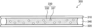
- FIGS. 6 to 9 are cross-sectional views illustrating the protection film of FIG. 3 according to some embodiments of the inventive concept.
- the protection film 300 may include a first film 310 , a second film 320 , a shear thickening fluid 330 , and a sealing member 340 .
- the first film 310 and the second film 320 may be disposed to face each other.
- Each of the first film 310 and the second film 320 may use a polyester-based resin, such as polyethylene terephthalate, polyethylene isophthalate, polybutylene terephthalate, and/or the like; a cellulose-based resin, such as diacetylcellulose, triacetylcellulose, and/or the like; a polycarbonate-based resin; an acryl-based resin, such as polymethyl (meth) acrylate, polyethyl (meth) acrylate, and/or the like; a styrene-based resin, such as polystyrene, an acrylonitrile-styrene copolymer, and/or the like; a polyolefin-based resin, such as polyethylene, polypropylene, polyolefin resin having a cyclo-based or norbornene structure, an ethylene-propylene copolymer, and/or the like; a vinyl chloride resin; a polyamide-based resin, such as nylon
- thermosetting resin such as an (meth) acrylic-based resin, a urethane-based resin, an epoxy-based resin, or a silicone-based resin, a film made of an ultraviolet curable resin, and/or the like, may be used.
- the shear thickening fluid 330 may include a dispersion fluid 332 for filling the gap between nanoparticles 331 and nanoparticles 331 .
- the nanoparticles 331 may be, for example, silica particles, but are not limited thereto.
- the dispersion fluid 332 may be, for example, polyethylene glycol (PEG), or ethylen glycol (EG), but is not limited thereto.
- the sealing member 340 may seal the gap between the first film 310 and the second film 320 to provide a sealed space therein.
- the shear thickening fluid 330 may be disposed in the space sealed by the sealing member 340 .
- a protection film 301 may include a first film 311 , a second film 321 , and the shear thickening fluid 330 .
- the first film 311 and the second film 321 may be composed of the same or substantially the same material as the first film 310 and the second film 320 described with reference to FIG. 6 .
- the first film 311 may include a first central portion 312 , and a first peripheral portion 313 surrounding the first central portion 312 .
- the second film 321 may include a second central portion 322 , and a second peripheral portion 323 surrounding the second central portion 322 .
- the first central portion 312 and the second central portion 322 may face each other, and the first peripheral portion 313 and the second peripheral portion 323 may face each other.
- the first peripheral portion 313 and the second peripheral portion 323 may be bonded to each other to provide a sealed space between the first central portion 312 and the second central portion 322 .
- the first peripheral portion 313 and the second peripheral portion 323 may be bonded through, for example, a laser welding process.
- the shear thickening fluid 330 may be disposed in the sealed space between the first central portion 312 and the second central portion 322 .
- a protection film 302 may include a fabric 350 and the shear thickening fluid 330 .
- the shear thickening fluid 330 may be impregnated into the fabric 350 .
- Materials composing the shear thickening fluid 330 were described with reference to FIG. 6 , and therefore, a specific description thereof will not be repeated.
- the fabric 350 may be formed of various fibers, and may include, for example, a synthetic fiber, a carbon fiber, a glass fiber, and/or the like.
- the protection film 302 may further include a first coating layer 361 and a second coating layer 362 .
- the first coating layer 361 may be disposed on an upper portion of the fabric 350 into which the shear thickening fluid 330 is impregnated.
- the second coating layer 362 may be disposed on a lower portion of the fabric 350 into which the shear thickening fluid 330 is impregnated.
- the first and second coating layers 361 and 362 may serve to protect the shear thickening fluid 330 from escaping from the fabric 350 .
- a protection film 303 may include a base film 370 and the shear thickening fluid 330 .
- a plurality of voids (e.g., pores) 371 may be defined on a surface of the base film 370 .
- the voids 371 may be provided on an upper surface of the base film 370 , and a lower surface thereof opposite the upper surface.
- the shear thickening fluid 330 may be disposed in the voids 371 of the base film 370 .
- the protection film 303 may further include a first coating layer 363 and a second coating layer 364 .
- the first coating layer 363 may be disposed on an upper portion of the base film 370 .
- the second coating layer 364 may be disposed on a lower portion of the base film 370 .
- the first and second coating layers 363 and 364 may serve to protect the shear thickening fluid 330 from escaping from the voids 371 of the base film 370 .
- FIG. 10A is a perspective view illustrating a rollable display apparatus 1001 in an unrolled state
- FIG. 10B is a perspective view illustrating the rollable display apparatus 1001 in a rolled state.
- the rollable display apparatus 1001 may include a housing HS, a display panel 101 , and a protection film 304 .
- the housing HS functions as a winding core for rolling the display panel 101 .
- the housing HS may have an approximate cylindrical shape.
- the protection film 304 may be bonded to a lower portion of the display panel 101 .
- the display panel 101 may be flexible.
- the display panel 101 may be the display panel 100 described with reference to FIGS. 3 to 5
- the protection film 304 may be one of the protection films 300 to 303 described with reference to FIGS. 6 to 9 .
- the display panel 101 having the protection film 304 bonded thereto may be fixed inside the housing HS.
- the rollable display apparatus 1001 may be operated in a rolled state and in an unrolled state.
- the display panel 101 having the protection film 304 bonded thereto may be rolled along the outer circumference of the housing HS.
- the display panel 101 having the protection film 304 bonded thereto may be unwound and unrolled in the direction opposite to the rolling direction.
- the protection film 304 may alleviate strain which may occur in the display panel 101 as the display panel 101 is rolled. Also, the impact resistance characteristic of the rollable display apparatus 1001 may be improved thanks to the protection film 304 , which temporarily becomes stiff when an impact equal to or greater than a reference value is applied thereto.
- FIG. 11A is a perspective view illustrating a stretchable display apparatus 1002 in an initial state
- FIG. 11B is a perspective view illustrating the stretchable display apparatus 1002 in a stretched state.
- the stretchable display apparatus 1002 may include a display panel 102 and the protection film 304 .
- the display panel 102 may be stretched by an external force.
- the external force is removed from the display panel 102 , the original state thereof may be restored.
- the term “stretched” means that a length or an area is extended when viewed from a plane, which is different from being folded or bent in one direction.
- the stretchable display apparatus 1002 in an initial state of FIG. 11 is exemplarily illustrated to have a first length WA in a horizontal direction DRH.
- the stretchable display apparatus 1002 in a stretched state of FIG. 11B is exemplarily illustrated to be extended by a length (e.g., predetermined length) WD in the horizontal direction DRH compared with the stretchable display apparatus 1002 in an initial state of FIG. 11A .
- the protection film 305 may be any one of the protection films 300 to 303 described with reference to FIGS. 6 to 9 .
- the protection film 305 is disposed on a lower portion of the display panel 102 to be stretched or restored as the display panel 102 is stretched or restored.
- the protection film 305 may alleviate strain which may occur in the display panel 102 as the display panel 102 is stretched. Also, the impact resistance characteristic of the stretchable display apparatus 1002 may be improved (e.g., increased) thanks to the protection film 305 , which temporarily becomes stiff when an impact equal to or greater than a reference value is applied thereto.
- first”, “second”, “third”, etc. may be used herein to describe various elements, components, regions, layers and/or sections, these elements, components, regions, layers and/or sections should not be limited by these terms. These terms are used to distinguish one element, component, region, layer or section from another element, component, region, layer or section. Thus, a first element, component, region, layer or section discussed below could be termed a second element, component, region, layer or section, without departing from the spirit and scope of the inventive concept.
- spatially relative terms such as “beneath”, “below”, “lower”, “under”, “above”, “upper” and the like, may be used herein for ease of description to describe one element or feature's relationship to another element(s) or feature(s) as illustrated in the figures. It will be understood that the spatially relative terms are intended to encompass different orientations of the device in use or in operation, in addition to the orientation depicted in the figures. For example, if the device in the figures is turned over, elements described as “below” or “beneath” or “under” other elements or features would then be oriented “above” the other elements or features. Thus, the example terms “below” and “under” can encompass both an orientation of above and below.
- the device may be otherwise oriented (e.g., rotated 90 degrees or at other orientations) and the spatially relative descriptors used herein should be interpreted accordingly.
- a layer is referred to as being “between” two layers, it can be the only layer between the two layers, or one or more intervening layers may also be present.
Landscapes
- Engineering & Computer Science (AREA)
- Signal Processing (AREA)
- Physics & Mathematics (AREA)
- Optics & Photonics (AREA)
- Microelectronics & Electronic Packaging (AREA)
- Electroluminescent Light Sources (AREA)
- Devices For Indicating Variable Information By Combining Individual Elements (AREA)
Abstract
Description
Claims (20)
Applications Claiming Priority (2)
| Application Number | Priority Date | Filing Date | Title |
|---|---|---|---|
| KR10-2017-0163549 | 2017-11-30 | ||
| KR1020170163549A KR20190064711A (en) | 2017-11-30 | 2017-11-30 | Display apparatus and mobile terminal |
Publications (2)
| Publication Number | Publication Date |
|---|---|
| US20190165314A1 US20190165314A1 (en) | 2019-05-30 |
| US11075358B2 true US11075358B2 (en) | 2021-07-27 |
Family
ID=66634552
Family Applications (1)
| Application Number | Title | Priority Date | Filing Date |
|---|---|---|---|
| US16/200,546 Active 2039-08-23 US11075358B2 (en) | 2017-11-30 | 2018-11-26 | Display apparatus and mobile terminal |
Country Status (2)
| Country | Link |
|---|---|
| US (1) | US11075358B2 (en) |
| KR (1) | KR20190064711A (en) |
Cited By (2)
| Publication number | Priority date | Publication date | Assignee | Title |
|---|---|---|---|---|
| US20210389805A1 (en) * | 2017-09-20 | 2021-12-16 | Intel Corporation | Apparatuses, methods, and systems for thermo-mechanical protection of electronics including computer components and sensors |
| US11522469B2 (en) * | 2019-12-06 | 2022-12-06 | Alliance For Sustainable Energy, Llc | Electric machines as motors and power generators |
Families Citing this family (6)
| Publication number | Priority date | Publication date | Assignee | Title |
|---|---|---|---|---|
| KR102534800B1 (en) * | 2018-02-13 | 2023-05-19 | 삼성디스플레이 주식회사 | Rollable display device |
| US11999844B2 (en) * | 2020-03-09 | 2024-06-04 | Rohm And Haas Electronic Materials Llc | Optically clear shear thickening fluids and optical display device comprising same |
| CN112071204B (en) * | 2020-09-11 | 2022-10-18 | 维沃移动通信有限公司 | Electronic device |
| KR20230041109A (en) * | 2021-09-15 | 2023-03-24 | 삼성디스플레이 주식회사 | Polymer layer and display device including the same |
| CN118366374A (en) * | 2024-04-26 | 2024-07-19 | 上海天马微电子有限公司 | Display module and display device |
| WO2026063729A1 (en) * | 2024-09-19 | 2026-03-26 | 삼성전자 주식회사 | Electronic device comprising flexible display assembly |
Citations (13)
| Publication number | Priority date | Publication date | Assignee | Title |
|---|---|---|---|---|
| WO2008115636A2 (en) * | 2007-02-13 | 2008-09-25 | Dow Global Technologies, Inc. | Plastic hollow fiber containing a shear-thickening fluid for high tensile strength fibers |
| US20120096630A1 (en) * | 2007-01-19 | 2012-04-26 | James Riddell Ferguson | Impact Shock Absorbing Material |
| US20140204293A1 (en) * | 2013-01-24 | 2014-07-24 | Lg Display Co., Ltd. | Display panel and display device including the same |
| US20160009593A1 (en) * | 2013-02-27 | 2016-01-14 | Corning Incorporated | Methods and structures for reducing biaxial bending and/or twisting of flexible glass substrates |
| US20160041679A1 (en) * | 2014-08-11 | 2016-02-11 | Samsung Display Co., Ltd. | Flexible organic light emitting diode display |
| US20160116814A1 (en) * | 2013-04-15 | 2016-04-28 | Sharp Kabushiki Kaisha | Display panel and display device |
| US9519370B2 (en) | 2013-05-31 | 2016-12-13 | Samsung Display Co., Ltd. | Display device and method for driving the same |
| KR101732488B1 (en) | 2015-06-15 | 2017-05-04 | 한국과학기술원 | Impact-resistant flexible composite using shear-thickening fluid and shape-variable protection apparatus |
| US20170373121A1 (en) * | 2017-04-05 | 2017-12-28 | Shanghai Tianma Micro-electronics Co., Ltd. | Flexible display panel and flexible display device |
| US9886116B2 (en) | 2012-07-26 | 2018-02-06 | Apple Inc. | Gesture and touch input detection through force sensing |
| US20180059727A1 (en) * | 2016-08-29 | 2018-03-01 | Samsung Display Co., Ltd. | Rollable display device |
| US20190187513A1 (en) * | 2017-12-20 | 2019-06-20 | Shanghai Tianma AM-OLED Co., Ltd. | Display device and fabrication method thereof |
| US20190380217A1 (en) * | 2016-12-01 | 2019-12-12 | 3M Innovative Properties Company | Electronic devices incorporating flexible component layers with interlocking devices |
-
2017
- 2017-11-30 KR KR1020170163549A patent/KR20190064711A/en not_active Ceased
-
2018
- 2018-11-26 US US16/200,546 patent/US11075358B2/en active Active
Patent Citations (13)
| Publication number | Priority date | Publication date | Assignee | Title |
|---|---|---|---|---|
| US20120096630A1 (en) * | 2007-01-19 | 2012-04-26 | James Riddell Ferguson | Impact Shock Absorbing Material |
| WO2008115636A2 (en) * | 2007-02-13 | 2008-09-25 | Dow Global Technologies, Inc. | Plastic hollow fiber containing a shear-thickening fluid for high tensile strength fibers |
| US9886116B2 (en) | 2012-07-26 | 2018-02-06 | Apple Inc. | Gesture and touch input detection through force sensing |
| US20140204293A1 (en) * | 2013-01-24 | 2014-07-24 | Lg Display Co., Ltd. | Display panel and display device including the same |
| US20160009593A1 (en) * | 2013-02-27 | 2016-01-14 | Corning Incorporated | Methods and structures for reducing biaxial bending and/or twisting of flexible glass substrates |
| US20160116814A1 (en) * | 2013-04-15 | 2016-04-28 | Sharp Kabushiki Kaisha | Display panel and display device |
| US9519370B2 (en) | 2013-05-31 | 2016-12-13 | Samsung Display Co., Ltd. | Display device and method for driving the same |
| US20160041679A1 (en) * | 2014-08-11 | 2016-02-11 | Samsung Display Co., Ltd. | Flexible organic light emitting diode display |
| KR101732488B1 (en) | 2015-06-15 | 2017-05-04 | 한국과학기술원 | Impact-resistant flexible composite using shear-thickening fluid and shape-variable protection apparatus |
| US20180059727A1 (en) * | 2016-08-29 | 2018-03-01 | Samsung Display Co., Ltd. | Rollable display device |
| US20190380217A1 (en) * | 2016-12-01 | 2019-12-12 | 3M Innovative Properties Company | Electronic devices incorporating flexible component layers with interlocking devices |
| US20170373121A1 (en) * | 2017-04-05 | 2017-12-28 | Shanghai Tianma Micro-electronics Co., Ltd. | Flexible display panel and flexible display device |
| US20190187513A1 (en) * | 2017-12-20 | 2019-06-20 | Shanghai Tianma AM-OLED Co., Ltd. | Display device and fabrication method thereof |
Cited By (3)
| Publication number | Priority date | Publication date | Assignee | Title |
|---|---|---|---|---|
| US20210389805A1 (en) * | 2017-09-20 | 2021-12-16 | Intel Corporation | Apparatuses, methods, and systems for thermo-mechanical protection of electronics including computer components and sensors |
| US11609614B2 (en) * | 2017-09-20 | 2023-03-21 | Intel Corporation | Apparatuses, methods, and systems for thermomechanical protection of electronics including computer components and sensors |
| US11522469B2 (en) * | 2019-12-06 | 2022-12-06 | Alliance For Sustainable Energy, Llc | Electric machines as motors and power generators |
Also Published As
| Publication number | Publication date |
|---|---|
| KR20190064711A (en) | 2019-06-11 |
| US20190165314A1 (en) | 2019-05-30 |
Similar Documents
| Publication | Publication Date | Title |
|---|---|---|
| US11075358B2 (en) | Display apparatus and mobile terminal | |
| US20250040341A1 (en) | Display device | |
| CN107665058B (en) | display screen | |
| TWI783170B (en) | Display device | |
| US11177454B2 (en) | Display apparatus | |
| US11720193B2 (en) | Display module | |
| US20200060028A1 (en) | Display device | |
| US9747822B2 (en) | Rollable display device | |
| CN111047983A (en) | Foldable display device | |
| US20150201487A1 (en) | Flexible display device | |
| EP3786770B1 (en) | Sensing unit, display device, and method of driving the display device | |
| KR102426130B1 (en) | Window member and display apparatus including the same | |
| CN110930886A (en) | Foldable display device | |
| CN113206134A (en) | Display device | |
| US20190243496A1 (en) | Display apparatus | |
| KR102792198B1 (en) | Display panel and display device including the same | |
| US11569478B2 (en) | Flexible display apparatus having improved reliability | |
| CN113257117A (en) | Display device | |
| KR102786570B1 (en) | Display apparatus and manufacturing method thereof | |
| CN118414901A (en) | Display device | |
| KR20210109086A (en) | Display device | |
| US20230030352A1 (en) | Display panel and electronic apparatus | |
| CN217639853U (en) | Electronic device | |
| US12566473B2 (en) | Display device |
Legal Events
| Date | Code | Title | Description |
|---|---|---|---|
| AS | Assignment |
Owner name: SAMSUNG DISPLAY CO., LTD., KOREA, REPUBLIC OF Free format text: ASSIGNMENT OF ASSIGNORS INTEREST;ASSIGNORS:KIM, SANGHOON;HWANG, SEONGJIN;REEL/FRAME:047585/0384 Effective date: 20181120 |
|
| FEPP | Fee payment procedure |
Free format text: ENTITY STATUS SET TO UNDISCOUNTED (ORIGINAL EVENT CODE: BIG.); ENTITY STATUS OF PATENT OWNER: LARGE ENTITY |
|
| STPP | Information on status: patent application and granting procedure in general |
Free format text: DOCKETED NEW CASE - READY FOR EXAMINATION |
|
| STPP | Information on status: patent application and granting procedure in general |
Free format text: NON FINAL ACTION MAILED |
|
| STPP | Information on status: patent application and granting procedure in general |
Free format text: RESPONSE TO NON-FINAL OFFICE ACTION ENTERED AND FORWARDED TO EXAMINER |
|
| STPP | Information on status: patent application and granting procedure in general |
Free format text: NOTICE OF ALLOWANCE MAILED -- APPLICATION RECEIVED IN OFFICE OF PUBLICATIONS |
|
| STPP | Information on status: patent application and granting procedure in general |
Free format text: PUBLICATIONS -- ISSUE FEE PAYMENT RECEIVED |
|
| STPP | Information on status: patent application and granting procedure in general |
Free format text: PUBLICATIONS -- ISSUE FEE PAYMENT VERIFIED |
|
| STCF | Information on status: patent grant |
Free format text: PATENTED CASE |
|
| MAFP | Maintenance fee payment |
Free format text: PAYMENT OF MAINTENANCE FEE, 4TH YEAR, LARGE ENTITY (ORIGINAL EVENT CODE: M1551); ENTITY STATUS OF PATENT OWNER: LARGE ENTITY Year of fee payment: 4 |