US11074986B2 - Shift register, gate driving circuit, and display device - Google Patents
Shift register, gate driving circuit, and display device Download PDFInfo
- Publication number
- US11074986B2 US11074986B2 US16/835,845 US202016835845A US11074986B2 US 11074986 B2 US11074986 B2 US 11074986B2 US 202016835845 A US202016835845 A US 202016835845A US 11074986 B2 US11074986 B2 US 11074986B2
- Authority
- US
- United States
- Prior art keywords
- terminal
- pull
- signal
- node
- transistor
- Prior art date
- Legal status (The legal status is an assumption and is not a legal conclusion. Google has not performed a legal analysis and makes no representation as to the accuracy of the status listed.)
- Expired - Fee Related
Links
Images


Classifications
-
- G—PHYSICS
- G09—EDUCATION; CRYPTOGRAPHY; DISPLAY; ADVERTISING; SEALS
- G09G—ARRANGEMENTS OR CIRCUITS FOR CONTROL OF INDICATING DEVICES USING STATIC MEANS TO PRESENT VARIABLE INFORMATION
- G09G3/00—Control arrangements or circuits, of interest only in connection with visual indicators other than cathode-ray tubes
- G09G3/20—Control arrangements or circuits, of interest only in connection with visual indicators other than cathode-ray tubes for presentation of an assembly of a number of characters, e.g. a page, by composing the assembly by combination of individual elements arranged in a matrix no fixed position being assigned to or needed to be assigned to the individual characters or partial characters
- G09G3/2092—Details of a display terminals using a flat panel, the details relating to the control arrangement of the display terminal and to the interfaces thereto
-
- G—PHYSICS
- G09—EDUCATION; CRYPTOGRAPHY; DISPLAY; ADVERTISING; SEALS
- G09G—ARRANGEMENTS OR CIRCUITS FOR CONTROL OF INDICATING DEVICES USING STATIC MEANS TO PRESENT VARIABLE INFORMATION
- G09G3/00—Control arrangements or circuits, of interest only in connection with visual indicators other than cathode-ray tubes
- G09G3/20—Control arrangements or circuits, of interest only in connection with visual indicators other than cathode-ray tubes for presentation of an assembly of a number of characters, e.g. a page, by composing the assembly by combination of individual elements arranged in a matrix no fixed position being assigned to or needed to be assigned to the individual characters or partial characters
- G09G3/34—Control arrangements or circuits, of interest only in connection with visual indicators other than cathode-ray tubes for presentation of an assembly of a number of characters, e.g. a page, by composing the assembly by combination of individual elements arranged in a matrix no fixed position being assigned to or needed to be assigned to the individual characters or partial characters by control of light from an independent source
- G09G3/36—Control arrangements or circuits, of interest only in connection with visual indicators other than cathode-ray tubes for presentation of an assembly of a number of characters, e.g. a page, by composing the assembly by combination of individual elements arranged in a matrix no fixed position being assigned to or needed to be assigned to the individual characters or partial characters by control of light from an independent source using liquid crystals
- G09G3/3611—Control of matrices with row and column drivers
- G09G3/3674—Details of drivers for scan electrodes
- G09G3/3677—Details of drivers for scan electrodes suitable for active matrices only
-
- G—PHYSICS
- G11—INFORMATION STORAGE
- G11C—STATIC STORES
- G11C19/00—Digital stores in which the information is moved stepwise, e.g. shift registers
- G11C19/28—Digital stores in which the information is moved stepwise, e.g. shift registers using semiconductor elements
-
- G—PHYSICS
- G09—EDUCATION; CRYPTOGRAPHY; DISPLAY; ADVERTISING; SEALS
- G09G—ARRANGEMENTS OR CIRCUITS FOR CONTROL OF INDICATING DEVICES USING STATIC MEANS TO PRESENT VARIABLE INFORMATION
- G09G2300/00—Aspects of the constitution of display devices
- G09G2300/08—Active matrix structure, i.e. with use of active elements, inclusive of non-linear two terminal elements, in the pixels together with light emitting or modulating elements
- G09G2300/0809—Several active elements per pixel in active matrix panels
- G09G2300/0842—Several active elements per pixel in active matrix panels forming a memory circuit, e.g. a dynamic memory with one capacitor
-
- G—PHYSICS
- G09—EDUCATION; CRYPTOGRAPHY; DISPLAY; ADVERTISING; SEALS
- G09G—ARRANGEMENTS OR CIRCUITS FOR CONTROL OF INDICATING DEVICES USING STATIC MEANS TO PRESENT VARIABLE INFORMATION
- G09G2310/00—Command of the display device
- G09G2310/02—Addressing, scanning or driving the display screen or processing steps related thereto
- G09G2310/0264—Details of driving circuits
- G09G2310/0286—Details of a shift registers arranged for use in a driving circuit
Definitions
- the present disclosure relates to the field of display technology, and more particularly, to a shift register, a gate driving circuit, and a display device.
- a gate driving circuit is generally used to send gate driving signals to pixel units of a display area line by line, so that the pixel units receive data signals line by line.
- the gate driving circuit generally includes multi-stage connected shift register, and an output terminal of each shift register is connected to a row of pixel units, and is configured to send the above gate driving signals to the pixel units.
- the purpose of the present disclosure is to provide a shift register, a gate driving circuit, and a display device.
- a shift register including a first signal output terminal, wherein the shift register further includes: a first switching, a second switching, a third switching, and a fourth switching.
- the first switching is connected to a first DC power signal terminal and a first node, and is configured to transmit a signal of the first DC power signal terminal to the first node in response to the signal of the first DC power signal terminal;
- the second switching is connected to a second DC power signal terminal, the first signal output terminal, and the first node, and is configured to transmit a signal of the second DC power signal terminal to the first node in response to a signal of the first signal output terminal;
- the third switching is connected to the first node, the second DC power signal terminal, and a second signal output terminal, and is configured to transmit the signal of the second DC power signal terminal to the second signal output terminal in response to a signal of the first node;
- the fourth switching is connected to the first DC power signal terminal and the second signal output terminal, and is configured to transmit the signal of the first DC power
- a gate driving circuit including the above shift register.
- a display device including the above gate driving circuit.
- FIG. 1 is a schematic structural view of a shift register in the related art
- FIG. 2 is a schematic structural view of an exemplary embodiment of a shift register according to the present disclosure
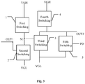
- FIG. 3 is a schematic structural view of another exemplary embodiment of a shift register according to the present disclosure.
- FIG. 4 is a schematic structural view of another exemplary embodiment of a shift register according to the present disclosure.
- FIG. 5 is a timing diagram of each node in FIG. 4 .
- a certain structure When a certain structure is “on” other structure(s), it may mean that the certain structure is integrally formed on the other structure(s), or that the certain structure is “directly” arranged on the other structure(s), or that the certain structure is “indirectly” arranged on other structure(s) through another structure.
- the shift register generally provides an output signal to its output terminal through a clock signal terminal, and the output signal is the gate driving signal.
- the widths of rising and falling edges of the gate driving signal are relatively long, which affects the charging time of the pixels in a display device, especially in a high-resolution display device, and this technical problem may seriously affect the display effect of the display device.
- the present disclosure is directed to provide a shift register, a gate driving circuit, and a display device, which are used to solve the technical problems in the related art that the widths of the rising and falling edges of the gate driving signal are relatively long, which affects the charging time of the pixels.
- FIG. 1 which is a schematic structural view of a shift register in the related art
- a signal of a clock signal terminal CLK is a clock pulse signal
- the clock signal terminal CKL outputs a pulse signal of an active level when an output terminal OUT needs to output a valid driving signal.
- the signal of the clock signal terminal CLK itself has rising and falling edges, the rising and falling edges of a gate driving signal output from the output terminal OUT are relatively long.
- FIG. 2 is a schematic structural view of an exemplary embodiment of a shift register according to the present disclosure.
- the shift register includes a first signal output terminal OUT 1 , and the shift register further includes: a first switching 1 , a second switching 2 , a third switching 3 , and a fourth switching 4 .
- the first switching 1 is connected to a first DC power signal terminal VGH and a first node N 1 , and is configured to transmit a signal of the first DC power signal terminal VGH to the first node N 1 in response to the signal of the first DC power signal terminal VGH;
- the second switching 2 is connected to a second DC power signal terminal VGL, the first signal output terminal OUT 1 , and the first node N 1 , and is configured to transmit a signal of the second DC power signal terminal VGL to the first node N 1 in response to a signal of the first signal output terminal OUT 1 ;
- the third switching 3 is connected to the first node N 1 , the second DC power signal terminal VGL, and a second signal output terminal OUT 2 , and is configured to transmit the signal of the second DC power signal terminal VGL to the second signal output terminal OUT 2 in response to a signal of the first node N 1 ;
- the fourth switching 4 is connected to the first DC power signal terminal VGH and the second signal output terminal OUT 2 , and is configured to
- the signal of the first DC power signal terminal is an active level signal
- the signal of the second DC power signal terminal is an in inactive level signal.
- the second switching is turned on to transmit the inactive level signal of the second DC power signal terminal to the first node N 1 .
- the fourth switching 4 is turned on under the active level signal of the first DC power signal terminal, so as to transmit the active level signal of the first DC power signal terminal to the second signal output terminal OUT 2 .
- the second switching is turned off, and the first switching is turned on under the active level signal of the first DC power signal terminal, so as to transmit the active level signal of the first DC power signal terminal to the first node N 1 , and the third switching 3 is turned on under the active level signal of the first node N 1 to transmit the invalid level signal of the second DC power signal terminal to the second signal output terminal OUT 2 .
- the present disclosure uses the signal of the first signal output terminal as the control signal of the second switching. Because the ON potential of the second switching is relatively low and the second switching has been turned on when the signal of the first signal output terminal is still in the rising edge and falling edge phases, the signal of the first DC power signal terminal may be used to resend the gate driving signal to the second signal output terminal, so as to reduce the widths of the rising edge and falling edge of the gate driving signal.
- the third switching is turned on by the signal of the first DC power signal terminal, so that the second signal output terminal is in communication with the second DC power signal terminal, thereby avoiding the leakage current from the first DC power signal terminal to the second signal output terminal from affecting the potential of the second signal output terminal.
- first to fourth switching may be switching transistors.
- the first to fourth switching may be N-type transistors; when the active level is low, the first to fourth switching may be P-type transistors.
- the shift register further includes a pull-down node PD
- the shift register further includes a fifth switching 5 , which is connected to the second DC power signal terminal VGL, the second signal output terminal OUT 2 , and the pull-down node PD, and is configured to transmit the signal of the second DC power signal terminal VGL to the second signal output terminal OUT 2 in response to a signal of the pull-down node PD.
- the pull-down node PD of the shift register outputs the active level
- the first signal output terminal OUT 1 should output the inactive level.
- the pull-down node may include a first pull-down node PD 1 and a second pull-down node PD 2 .
- the shift register may further include: an input circuit 6 , an output circuit 7 , a pull-down control circuit, a first pull-down circuit 91 , a second pull-down circuit 92 , and a reset circuit 10 .
- the input circuit 6 is connected to an input signal terminal STV and a pull-up node PU, and is configured to transmit a signal of the input signal terminal STV to the pull-up node PU in response to the signal of the input signal terminal STV;
- the output circuit 7 is connected to a clock signal terminal CLK, the first signal output terminal OUT 1 , and the pull-up node PU, and is configured to transmit the signal of the clock signal terminal CLK to the first signal output terminal OUT 1 in response to a signal of the pull-up node PU;
- the pull-down control circuit is connected to a third power signal terminal VDD 2 , a fourth power signal terminal VDD 1 , a fifth power signal terminal VSS, the pull-up node PU, the first pull-down node PD 1 , and the second pull-down node PD 2 , and is configured to transmit a signal of the fifth power signal terminal VSS to the first pull-down node PD 1 and the second pull-down node PD 2 in response to
- the signal of the fifth power signal terminal VSS is an inactive level signal
- the signals of the third power signal terminal VDD 2 and the fourth power signal terminal VDD 1 are alternately active level signals. Such an arrangement may avoid the technical problem of the transistor threshold drift in the pull-down control circuit and the pull-down circuit.
- the pull-down control circuit may include a first pull-down control circuit 81 and a second pull-down control circuit 82 .
- the first pull-down control circuit 81 is connected to the third power signal terminal VDD 2 , the fifth power signal terminal VSS, a first pull-down control node PD-CN 1 , the first pull-down node PD 1 , and the pull-up node PU, and is configured to transmit the signal of the fifth power signal terminal VSS to the first pull-down node PD 1 and the first pull-down control node PD-CN 1 in response to the signal of the pull-up node PU, and transmit the signal of the third power signal terminal VDD 2 to the first pull-down node PD 1 and the first pull-down control node PD-CN 1 in response to the signal of the third power signal terminal VDD 2 ; and the second pull-down control circuit 82 is connected to the fourth power signal terminal VDD 1 , the fifth power signal terminal VSS, a second pull-down control node
- the first switching 1 may include a first transistor T 1 , a first terminal of the first transistor T 1 is connected to the first DC power signal terminal VGH, a second terminal thereof is connected to the first node N 1 , and a control terminal thereof is connected to the first DC power signal terminal VGH;
- the second switching 2 may include a second transistor T 2 , a first terminal of the second transistor T 2 is connected to the second DC power signal terminal VGL, a second terminal thereof is connected to the first node N 1 , and a control terminal thereof is connected to the first signal output terminal OUT 1 ;
- the third switching 3 may include a third transistor T 3 , and a first terminal of the third transistor T 3 is connected to the second DC power signal terminal VGL, a second terminal thereof is connected to the second signal output terminal OUT 2 , and a control terminal thereof is connected to the first node N 1 ;
- the fourth switching 4 may include a fourth transistor T 4 , a first terminal of the fourth transistor T 4 is connected to the
- the input circuit 6 may include a sixth transistor T 6 , a first terminal of the sixth transistor T 6 is connected to the input signal terminal STV, and a second terminal thereof is connected to the pull-up node PU, and a control terminal thereof is connected to the input signal terminal STV; and the output circuit 7 may include a seventh transistor T 7 and a capacitor C, a first terminal of the seventh transistor T 7 is connected to the clock signal terminal CLK, and a second terminal thereof is connected to the first signal output terminal OUT 1 , and a control terminal thereof is connected to the pull-up node PU; and the capacitor C is connected between the pull-up node PU and the first signal output terminal OUT 1 .
- the first pull-down control circuit 81 may include an eighth transistor T 8 , a ninth transistor T 9 , a tenth transistor T 10 , and an eleventh transistor T 11 .
- a first terminal of the eighth transistor T 8 is connected to the third power signal terminal VDD 2 , a control terminal thereof is connected to the third power signal terminal VDD 2 , and a second terminal thereof is connected to the first pull-down control node PD-CN 1 ;
- a first terminal of the ninth transistor T 9 is connected to the third power signal terminal VDD 2 , a control terminal thereof is connected to the first pull-down control node PD-CN 1 , and a second terminal thereof is connected to the first pull-down node PD 1 ;
- a first terminal of the tenth transistor T 10 is connected to the first pull-down control node PD-CN 1 , a second terminal thereof is connected to the fifth power signal terminal VSS, and a control terminal thereof is connected to the pull-up node PU; and a first terminal of the eleven
- the second pull-down control circuit 82 may include a twelfth transistor T 12 , a thirteenth transistor T 13 , a fourteenth transistor T 14 , and a fifteenth transistor T 15 .
- a first terminal of the twelfth transistor T 12 is connected to the fourth power signal terminal VDD 1 , a second terminal thereof is connected to the second pull-down control node PD-CN 2 , and a control terminal thereof is connected to the fourth power signal terminal VDD 1 ;
- a first terminal of the thirteenth transistor T 13 is connected to the fourth power signal terminal VDD 1 , a second terminal thereof is connected to the second pull-down node PD 2 , and a control terminal thereof is connected to the second pull-down control node PD-CN 2 ;
- a first terminal of the fourteenth transistor T 14 is connected to the first pull-down control node PD-CN 1 , a second terminal thereof is connected to the fifth power signal terminal VSS, and a control terminal thereof is connected to the pull-up node
- the first pull-down circuit 91 may include: a sixteenth transistor T 16 and a seventeenth transistor T 17 .
- a first terminal of the sixteenth transistor T 16 is connected to the fifth power signal terminal VSS, a second terminal thereof is connected to the pull-up node PU, and a control terminal thereof is connected to the first pull-down node PD 1 ; and a first terminal of the seventeenth transistor T 17 is connected to the fifth power signal terminal VSS, and a second terminal thereof is connected to the first signal output terminal OUT 1 , and a control terminal thereof is connected to the first pull-down node PD 1 .
- the second pull-down circuit 92 may include an eighteenth transistor T 18 and a nineteenth transistor T 19 .
- a first terminal of the eighteenth transistor T 18 is connected to the fifth power signal terminal VSS, a second terminal thereof is connected to the pull-up node PU, and a control terminal thereof is connected to the second pull-down node PD 2 ; and a first terminal of the nineteenth transistor T 19 is connected to the fifth power signal terminal VSS, a second terminal thereof is connected to the first signal output terminal OUT 1 , and a control terminal thereof is connected to the second pull-down node PD 2 .
- the reset circuit 10 may include a twentieth transistor T 20 , a first terminal of the twentieth transistor T 20 is connected to the fifth power signal terminal VSS, a second terminal thereof is connected to the pull-up node PU, and a control terminal thereof is connected to the reset signal terminal REST.
- FIG. 5 which is a timing diagram of each node in FIG. 4 , it can be seen from FIG. 5 that the rising and falling edges of the gate driving signal output from the first signal output terminal OUT 1 are significantly wider than those of the gate driving signal output from the second signal output terminal OUT 2 .
- the structure of the shift register for generating the gate driving signal to the first signal output terminal OUT has more options, and these all fall within the scope of the present disclosure.
- the present exemplary embodiment further provides a gate driving circuit including the above shift register.
- the gate driving circuit has the same technical features and working principle as the above shift register. The above contents have been described in detail, and are not repeated here.
- the present exemplary embodiment further provides a display device including the above gate driving circuit.
- the display device has the same technical features and working principle as the above gate driving circuit. The above contents have been described in detail, and are not repeated here.
Landscapes
- Engineering & Computer Science (AREA)
- Physics & Mathematics (AREA)
- Computer Hardware Design (AREA)
- General Physics & Mathematics (AREA)
- Theoretical Computer Science (AREA)
- Chemical & Material Sciences (AREA)
- Crystallography & Structural Chemistry (AREA)
- Shift Register Type Memory (AREA)
- Liquid Crystal Display Device Control (AREA)
- Control Of Indicators Other Than Cathode Ray Tubes (AREA)
Abstract
Description
Claims (14)
Applications Claiming Priority (2)
| Application Number | Priority Date | Filing Date | Title |
|---|---|---|---|
| CN201910688713.4A CN112309295B (en) | 2019-07-29 | 2019-07-29 | Shift register unit, gate drive circuit, display device |
| CN201910688713.4 | 2019-07-29 |
Publications (2)
| Publication Number | Publication Date |
|---|---|
| US20210035651A1 US20210035651A1 (en) | 2021-02-04 |
| US11074986B2 true US11074986B2 (en) | 2021-07-27 |
Family
ID=74260518
Family Applications (1)
| Application Number | Title | Priority Date | Filing Date |
|---|---|---|---|
| US16/835,845 Expired - Fee Related US11074986B2 (en) | 2019-07-29 | 2020-03-31 | Shift register, gate driving circuit, and display device |
Country Status (2)
| Country | Link |
|---|---|
| US (1) | US11074986B2 (en) |
| CN (1) | CN112309295B (en) |
Citations (3)
| Publication number | Priority date | Publication date | Assignee | Title |
|---|---|---|---|---|
| US20120293737A1 (en) * | 2011-05-16 | 2012-11-22 | Chengdu Boe Optoelectronics Technology Co., Ltd. | Shift register unit circuit, shift register, array substrate and liquid crystal display |
| US20130136224A1 (en) * | 2011-11-25 | 2013-05-30 | Chengdu Boe Optoelectronics Technology Co., Ltd. | Shift register, gate driver, and display device |
| US20160189795A1 (en) * | 2014-12-30 | 2016-06-30 | Shanghai Avic Optoelectronics Co., Ltd | Shift register, method and system for operating shift register |
Family Cites Families (8)
| Publication number | Priority date | Publication date | Assignee | Title |
|---|---|---|---|---|
| CN103021358B (en) * | 2012-12-07 | 2015-02-11 | 京东方科技集团股份有限公司 | Shifting register unit, gate driving circuit and display device |
| CN103559913A (en) * | 2013-11-14 | 2014-02-05 | 友达光电股份有限公司 | a shift register |
| CN104715734B (en) * | 2015-04-14 | 2017-08-08 | 京东方科技集团股份有限公司 | Shift register, gate driving circuit and display device |
| CN108564907B (en) * | 2018-01-23 | 2021-01-26 | 京东方科技集团股份有限公司 | Shifting register unit, grid driving circuit and driving method thereof and display device |
| CN109935197B (en) * | 2018-02-14 | 2021-02-26 | 京东方科技集团股份有限公司 | Shift register unit, gate driving circuit, display device and driving method |
| CN108682397A (en) * | 2018-07-27 | 2018-10-19 | 京东方科技集团股份有限公司 | Shift register cell, gate driving circuit, display device and driving method |
| CN109658888B (en) * | 2019-01-02 | 2022-01-14 | 合肥京东方光电科技有限公司 | Shifting register unit, driving method, grid driving circuit and display device |
| CN109859670A (en) * | 2019-03-28 | 2019-06-07 | 京东方科技集团股份有限公司 | A shift register unit, its driving method, and gate driving circuit |
-
2019
- 2019-07-29 CN CN201910688713.4A patent/CN112309295B/en active Active
-
2020
- 2020-03-31 US US16/835,845 patent/US11074986B2/en not_active Expired - Fee Related
Patent Citations (3)
| Publication number | Priority date | Publication date | Assignee | Title |
|---|---|---|---|---|
| US20120293737A1 (en) * | 2011-05-16 | 2012-11-22 | Chengdu Boe Optoelectronics Technology Co., Ltd. | Shift register unit circuit, shift register, array substrate and liquid crystal display |
| US20130136224A1 (en) * | 2011-11-25 | 2013-05-30 | Chengdu Boe Optoelectronics Technology Co., Ltd. | Shift register, gate driver, and display device |
| US20160189795A1 (en) * | 2014-12-30 | 2016-06-30 | Shanghai Avic Optoelectronics Co., Ltd | Shift register, method and system for operating shift register |
Also Published As
| Publication number | Publication date |
|---|---|
| US20210035651A1 (en) | 2021-02-04 |
| CN112309295A (en) | 2021-02-02 |
| CN112309295B (en) | 2023-12-08 |
Similar Documents
| Publication | Publication Date | Title |
|---|---|---|
| US12039949B2 (en) | Shift register unit, gate driving circuit, display device, and driving method | |
| US11475825B2 (en) | Shift register unit, gate driving circuit, display device, and driving method | |
| US10923208B2 (en) | Shift register unit, shift register circuit and display device | |
| US11069281B2 (en) | Shift register unit, gate driving circuit, display device, and driving method | |
| US11250750B2 (en) | Shift register circuit, and driving method thereof, gate drive circuit and display device | |
| US10984879B2 (en) | Shift register unit and method for driving the same, gate driving circuit and display apparatus | |
| US10297204B2 (en) | Shift register unit, driving method, gate driving circuit and display device | |
| US10706758B2 (en) | Shift register unit, driving method thereof and display device | |
| US10872546B2 (en) | Shift register unit and method for driving the same, gate driving circuit and display apparatus | |
| US11244595B2 (en) | Shift register unit comprising input circuit, first control circuit, blanking control circuit, first output circuit, and second output circuit, driving method, gate driving circuit, and display device | |
| US10976866B2 (en) | Shift-register circuit, gate drive circuit, liquid crystal display and touch panel | |
| US10650768B2 (en) | Shift register unit and driving method thereof, gate driving circuit and display panel | |
| US10971102B2 (en) | Shift register unit and driving method, gate driving circuit, and display device | |
| US20170193945A1 (en) | Shift register unit, gate driving circuit and display device | |
| WO2013174118A1 (en) | Shift register, driver, and display | |
| US11727853B2 (en) | Shift register unit, gate driving circuit, display device, and driving method | |
| US11081035B2 (en) | Shift register unit, driving method, gate driving circuit and display panel | |
| US11942041B2 (en) | Shift register unit, gate driving circuit, display device, and driving method | |
| US10909893B2 (en) | Shift register circuit, GOA circuit, display device and method for driving the same | |
| US11217321B2 (en) | Shift register and driving method, gate driving circuit, and display device | |
| US9564889B2 (en) | Gate driving circuit and display device having the same | |
| CN110634436B (en) | Grid driving circuit and display panel | |
| US11640795B2 (en) | Shift register unit, gate drive circuit and drive method | |
| US11074986B2 (en) | Shift register, gate driving circuit, and display device |
Legal Events
| Date | Code | Title | Description |
|---|---|---|---|
| AS | Assignment |
Owner name: BOE TECHNOLOGY GROUP CO., LTD., CHINA Free format text: ASSIGNMENT OF ASSIGNORS INTEREST;ASSIGNORS:HU, SHENGHUA;NIE, CHUNYANG;ZHU, LIXIN;REEL/FRAME:052273/0070 Effective date: 20200211 Owner name: HEFEI XINSHENG OPTOELECTRONICS TECHNOLOGY CO., LTD., CHINA Free format text: ASSIGNMENT OF ASSIGNORS INTEREST;ASSIGNORS:HU, SHENGHUA;NIE, CHUNYANG;ZHU, LIXIN;REEL/FRAME:052273/0070 Effective date: 20200211 |
|
| FEPP | Fee payment procedure |
Free format text: ENTITY STATUS SET TO UNDISCOUNTED (ORIGINAL EVENT CODE: BIG.); ENTITY STATUS OF PATENT OWNER: LARGE ENTITY |
|
| STPP | Information on status: patent application and granting procedure in general |
Free format text: NON FINAL ACTION MAILED |
|
| STPP | Information on status: patent application and granting procedure in general |
Free format text: RESPONSE TO NON-FINAL OFFICE ACTION ENTERED AND FORWARDED TO EXAMINER |
|
| STPP | Information on status: patent application and granting procedure in general |
Free format text: NOTICE OF ALLOWANCE MAILED -- APPLICATION RECEIVED IN OFFICE OF PUBLICATIONS |
|
| STPP | Information on status: patent application and granting procedure in general |
Free format text: PUBLICATIONS -- ISSUE FEE PAYMENT RECEIVED |
|
| STPP | Information on status: patent application and granting procedure in general |
Free format text: PUBLICATIONS -- ISSUE FEE PAYMENT VERIFIED |
|
| STCF | Information on status: patent grant |
Free format text: PATENTED CASE |
|
| FEPP | Fee payment procedure |
Free format text: MAINTENANCE FEE REMINDER MAILED (ORIGINAL EVENT CODE: REM.); ENTITY STATUS OF PATENT OWNER: LARGE ENTITY |
|
| LAPS | Lapse for failure to pay maintenance fees |
Free format text: PATENT EXPIRED FOR FAILURE TO PAY MAINTENANCE FEES (ORIGINAL EVENT CODE: EXP.); ENTITY STATUS OF PATENT OWNER: LARGE ENTITY |
|
| STCH | Information on status: patent discontinuation |
Free format text: PATENT EXPIRED DUE TO NONPAYMENT OF MAINTENANCE FEES UNDER 37 CFR 1.362 |
|
| FP | Lapsed due to failure to pay maintenance fee |
Effective date: 20250727 |