US11065734B2 - Film thickness measuring device and polishing device - Google Patents
Film thickness measuring device and polishing device Download PDFInfo
- Publication number
- US11065734B2 US11065734B2 US14/644,501 US201514644501A US11065734B2 US 11065734 B2 US11065734 B2 US 11065734B2 US 201514644501 A US201514644501 A US 201514644501A US 11065734 B2 US11065734 B2 US 11065734B2
- Authority
- US
- United States
- Prior art keywords
- film thickness
- sensor
- polishing table
- thickness measuring
- trigger
- Prior art date
- Legal status (The legal status is an assumption and is not a legal conclusion. Google has not performed a legal analysis and makes no representation as to the accuracy of the status listed.)
- Active, expires
Links
Images


Classifications
-
- B—PERFORMING OPERATIONS; TRANSPORTING
- B24—GRINDING; POLISHING
- B24B—MACHINES, DEVICES, OR PROCESSES FOR GRINDING OR POLISHING; DRESSING OR CONDITIONING OF ABRADING SURFACES; FEEDING OF GRINDING, POLISHING, OR LAPPING AGENTS
- B24B37/00—Lapping machines or devices; Accessories
- B24B37/005—Control means for lapping machines or devices
- B24B37/013—Devices or means for detecting lapping completion
-
- B—PERFORMING OPERATIONS; TRANSPORTING
- B24—GRINDING; POLISHING
- B24B—MACHINES, DEVICES, OR PROCESSES FOR GRINDING OR POLISHING; DRESSING OR CONDITIONING OF ABRADING SURFACES; FEEDING OF GRINDING, POLISHING, OR LAPPING AGENTS
- B24B37/00—Lapping machines or devices; Accessories
- B24B37/005—Control means for lapping machines or devices
-
- B—PERFORMING OPERATIONS; TRANSPORTING
- B24—GRINDING; POLISHING
- B24B—MACHINES, DEVICES, OR PROCESSES FOR GRINDING OR POLISHING; DRESSING OR CONDITIONING OF ABRADING SURFACES; FEEDING OF GRINDING, POLISHING, OR LAPPING AGENTS
- B24B49/00—Measuring or gauging equipment for controlling the feed movement of the grinding tool or work; Arrangements of indicating or measuring equipment, e.g. for indicating the start of the grinding operation
- B24B49/10—Measuring or gauging equipment for controlling the feed movement of the grinding tool or work; Arrangements of indicating or measuring equipment, e.g. for indicating the start of the grinding operation involving electrical means
- B24B49/105—Measuring or gauging equipment for controlling the feed movement of the grinding tool or work; Arrangements of indicating or measuring equipment, e.g. for indicating the start of the grinding operation involving electrical means using eddy currents
-
- H—ELECTRICITY
- H01—ELECTRIC ELEMENTS
- H01L—SEMICONDUCTOR DEVICES NOT COVERED BY CLASS H10
- H01L21/00—Processes or apparatus adapted for the manufacture or treatment of semiconductor or solid state devices or of parts thereof
- H01L21/67—Apparatus specially adapted for handling semiconductor or electric solid state devices during manufacture or treatment thereof; Apparatus specially adapted for handling wafers during manufacture or treatment of semiconductor or electric solid state devices or components ; Apparatus not specifically provided for elsewhere
- H01L21/67005—Apparatus not specifically provided for elsewhere
- H01L21/67011—Apparatus for manufacture or treatment
- H01L21/67092—Apparatus for mechanical treatment
-
- B—PERFORMING OPERATIONS; TRANSPORTING
- B24—GRINDING; POLISHING
- B24B—MACHINES, DEVICES, OR PROCESSES FOR GRINDING OR POLISHING; DRESSING OR CONDITIONING OF ABRADING SURFACES; FEEDING OF GRINDING, POLISHING, OR LAPPING AGENTS
- B24B49/00—Measuring or gauging equipment for controlling the feed movement of the grinding tool or work; Arrangements of indicating or measuring equipment, e.g. for indicating the start of the grinding operation
-
- H—ELECTRICITY
- H01—ELECTRIC ELEMENTS
- H01L—SEMICONDUCTOR DEVICES NOT COVERED BY CLASS H10
- H01L21/00—Processes or apparatus adapted for the manufacture or treatment of semiconductor or solid state devices or of parts thereof
- H01L21/02—Manufacture or treatment of semiconductor devices or of parts thereof
- H01L21/04—Manufacture or treatment of semiconductor devices or of parts thereof the devices having at least one potential-jump barrier or surface barrier, e.g. PN junction, depletion layer or carrier concentration layer
- H01L21/18—Manufacture or treatment of semiconductor devices or of parts thereof the devices having at least one potential-jump barrier or surface barrier, e.g. PN junction, depletion layer or carrier concentration layer the devices having semiconductor bodies comprising elements of Group IV of the Periodic System or AIIIBV compounds with or without impurities, e.g. doping materials
- H01L21/30—Treatment of semiconductor bodies using processes or apparatus not provided for in groups H01L21/20 - H01L21/26
- H01L21/302—Treatment of semiconductor bodies using processes or apparatus not provided for in groups H01L21/20 - H01L21/26 to change their surface-physical characteristics or shape, e.g. etching, polishing, cutting
- H01L21/304—Mechanical treatment, e.g. grinding, polishing, cutting
-
- H—ELECTRICITY
- H01—ELECTRIC ELEMENTS
- H01L—SEMICONDUCTOR DEVICES NOT COVERED BY CLASS H10
- H01L21/00—Processes or apparatus adapted for the manufacture or treatment of semiconductor or solid state devices or of parts thereof
- H01L21/02—Manufacture or treatment of semiconductor devices or of parts thereof
- H01L21/04—Manufacture or treatment of semiconductor devices or of parts thereof the devices having at least one potential-jump barrier or surface barrier, e.g. PN junction, depletion layer or carrier concentration layer
- H01L21/18—Manufacture or treatment of semiconductor devices or of parts thereof the devices having at least one potential-jump barrier or surface barrier, e.g. PN junction, depletion layer or carrier concentration layer the devices having semiconductor bodies comprising elements of Group IV of the Periodic System or AIIIBV compounds with or without impurities, e.g. doping materials
- H01L21/30—Treatment of semiconductor bodies using processes or apparatus not provided for in groups H01L21/20 - H01L21/26
- H01L21/302—Treatment of semiconductor bodies using processes or apparatus not provided for in groups H01L21/20 - H01L21/26 to change their surface-physical characteristics or shape, e.g. etching, polishing, cutting
- H01L21/306—Chemical or electrical treatment, e.g. electrolytic etching
- H01L21/30625—With simultaneous mechanical treatment, e.g. mechanico-chemical polishing
-
- H—ELECTRICITY
- H01—ELECTRIC ELEMENTS
- H01L—SEMICONDUCTOR DEVICES NOT COVERED BY CLASS H10
- H01L22/00—Testing or measuring during manufacture or treatment; Reliability measurements, i.e. testing of parts without further processing to modify the parts as such; Structural arrangements therefor
Definitions
- the present invention relates to a film thickness measuring device and a polishing device.
- a polishing device for performing CMP includes a polishing table to which a polishing pad is pasted, and a top ring for holding a subject to be polished (for example, a substrate such as a semiconductor wafer or various films formed on a surface of the substrate).
- the polishing device polishes the subject to be polished by pressing the subject to be polished held at the top ring against the polishing pad while rotating the polishing table.
- the polishing device includes a film thickness measuring device for detecting an end point of polishing process based on the film thickness of the subject to be polished.
- the film thickness measuring device includes a film thickness measuring sensor for detecting the film thickness of the subject to be polished.
- Typical film thickness measuring sensors include an eddy current sensor (R-ECM) and an optical sensor (S-OPM).
- the eddy current sensor or the optical sensor is disposed in a hole formed at the polishing table so as to face the subject to be polished through the polishing pad.
- the eddy current sensor induces an eddy current at the subject to be polished such as a conductive film and detects the thickness of the subject to be polished from change of a magnetic field generated by the eddy current induced at the subject to be polished.
- the optical sensor irradiates the subject to be polished with light and detects the thickness of the subject to be polished by measuring an interference wave reflected from the subject to be polished.
- polishing table on which the film thickness measuring sensor is disposed rotates, during polishing process, a state where the subject to be polished exists above the film thickness measuring sensor and a state where the subject to be polished does not exist above the film thickness measuring sensor, appear alternately.
- the film thickness measuring sensor starts measurement before the subject to be polished starts to exist above the film thickness measuring sensor and finishes measurement after the subject to be polished no longer exists above the film thickness measuring sensor. Therefore, in the conventional technique, a trigger sensor for detecting that the polishing table makes one revolution is provided.
- the trigger sensor is comprised of, for example, a dog disposed outside the polishing table, and a proximity sensor disposed at the polishing table, the proximity sensor detecting the dog every time the polishing table makes one revolution.
- the polishing device of the conventional technique detects a timing for starting measurement and a timing for finishing measurement of the film thickness measuring sensor based on the output of the trigger sensor.
- Patent Literature 1 Japanese Patent Laid-Open No. 2009-233853
- Patent Literature 2 National Publication of International Patent Application No. 2002-529686
- the conventional technique does not take into account improvement of versatility of a film thickness measuring device.
- polishing devices in which a polishing table is configured to be able to rotate both in a clockwise direction and in a counterclockwise direction, and a rotation direction of the polishing table is reversed.
- a position where a trigger sensor a proximity sensor and a dog
- an object of the present invention is to improve versatility of the film thickness measuring device.
- a film thickness measuring device has been made in view of the above-described problems, and is a film thickness measuring device configured to measure a film thickness of a subject to be polished by a polishing device including a polishing table configured to rotate in a clockwise direction and in a counterclockwise direction, and a holding unit configured to rotate while holding the subject to be polished, the film thickness measuring device including a trigger sensor comprising a first member disposed at the polishing table and a second member disposed outside the polishing table, the trigger sensor configured to output a trigger signal indicating that the polishing table makes one revolution based on positional relationship between the first member and the second member, and a film thickness measuring sensor disposed at the polishing table, the film thickness measuring sensor configured to measure the film thickness of the subject to be polished at a timing based on the trigger signal output from the trigger sensor, the second member being disposed in an opposite region located at the opposite side of a rotation axis of the holding unit with respect to a rotation axis of the polishing table, the trigger sensor comprising a first
- the second member may be disposed on a plane passing through the rotation axis of the holding unit and the rotation axis of the polishing table, in the opposite region, and the film thickness measuring sensor and the first member may be disposed at the polishing table so as to be located on the plane passing through the rotation axis of the holding unit and the rotation axis of the polishing table, in the opposite region when the trigger signal is output from the trigger sensor.
- the second member may be a dog disposed outside the polishing table, and the first member may be a proximity sensor detecting the dog every time the polishing table makes one revolution.
- the film thickness measuring device may include a plurality of film thickness measuring sensors, and may further include a timing signal generator configured to output a timing for starting measurement and a timing for finishing measurement for each of the plurality of film thickness measuring sensors based on the trigger signal output from the trigger sensor.
- one film thickness measuring sensor among the plurality of film thickness measuring sensors may be disposed at the polishing table so as to be located in the opposite region when the trigger signal is output from the trigger sensor, and film thickness measuring sensors other than the one film thickness measuring sensor may be disposed in a region different from a region where the one film thickness measuring sensor is disposed.
- the timing signal generator may output a timing for starting measurement and a timing for finishing measurement for each of the plurality of film thickness measuring sensors based on the trigger signal, the rotation direction of the polishing table, positional relationship of the plurality of film thickness measuring sensors with respect to the proximity sensor, and rotation speed of the polishing table.
- the film thickness measuring device includes a film thickness measuring device according to any of the above, a polishing table to which a polishing pad for polishing the subject to be polished is pasted, a first driving unit configured to rotate the polishing table in a clockwise direction and in a counterclockwise direction, a holding unit configured to hold the subject to be polished and pressing the subject to be polished against the polishing pad, and a second driving unit configured to rotate the holding unit.
- FIG. 1 is a diagram schematically illustrating an overall structure of a polishing device according to a first embodiment
- FIG. 2 is a plan view illustrating positional relationship among a top ring, an eddy current sensor and a trigger sensor;
- FIG. 3 is a plan view illustrating positional relationship among the top ring, the eddy current sensor and the trigger sensor;
- FIG. 4 is a diagram schematically illustrating an overall structure of a polishing device according to a second embodiment
- FIG. 5 is a plan view illustrating positional relationship among the top ring, the eddy current sensor, an optical sensor, and the trigger sensor;
- FIG. 6 is a plan view illustrating positional relationship among the top ring, the eddy current sensor, the optical sensor and the trigger sensor;
- FIG. 7 is a plan view illustrating positional relationship among the top ring, the eddy current sensor, two optical sensors and the trigger sensor;
- FIG. 8 is a plan view illustrating positional relationship among the top ring, the eddy current sensor, the two optical sensors and the trigger sensor.
- FIG. 1 is a diagram schematically illustrating an overall structure of a polishing device according to the first embodiment.
- the polishing device 100 includes a polishing table 110 on which a polishing pad 108 for polishing a subject to be polished (for example, a substrate such as a semiconductor wafer or various films formed on a surface of the substrate) 102 can be placed on a top face.
- the polishing device 100 includes a first electric motor 112 rotationally driving the polishing table 110 in a clockwise direction and in a counterclockwise direction.
- the polishing device 100 includes a top ring (holding unit) 116 capable of holding the subject to be polished 102 .
- the polishing device 100 includes a second electric motor 118 rotationally driving the top ring 116 .
- the polishing device 100 includes a slurry line 120 supplying polishing liquid including a polishing agent to the top face of the polishing pad 108 . Still further, the polishing device 100 includes a polishing device control unit 140 outputting various control signals regarding the polishing device 100 .
- the polishing device 100 supplies polishing slurry including polishing abrasive grains from the slurry line 120 to the top face of the polishing pad 108 and rotationally drives the polishing table 110 by the first electric motor 112 .
- the polishing device 100 then presses the subject to be polished 102 held by the top ring 116 against the polishing pad 108 while rotating the top ring 116 around a rotation axis which is eccentric from a rotation axis of the polishing table 110 .
- the subject to be polished 102 is polished by the polishing pad 108 holding the polishing slurry and becomes flat.
- the film thickness measuring device 200 includes an eddy current sensor 210 and a trigger sensor 220 . Further, the film thickness measuring device 200 includes a timing signal generator 230 connected to the eddy current sensor 210 and the trigger sensor 220 via rotary joint connectors 160 and 170 . Further, the film thickness measuring device 200 includes an end point detector 240 connected to the eddy current sensor 210 via the rotary joint connectors 160 and 170 .
- the trigger sensor 220 includes a proximity sensor 222 (first member) disposed at the polishing table 110 and a dog 224 (second member) disposed outside the polishing table 110 .
- a hole into which the eddy current sensor 210 can be inserted from a reverse side of the polishing table 110 is formed.
- the eddy current sensor 210 is inserted into the hole formed at the polishing table 110 . It should be noted that the polishing table 110 is connected to the ground.
- the eddy current sensor 210 includes an exciting coil, a detection coil and a balance coil.
- the exciting coil is excited by an AC current supplied from an AC source and forms an eddy current at the subject to be polished 102 disposed near the exciting coil.
- a magnetic flux generated by the eddy current formed at the subject to be polished 102 interlinks with the detection coil and the balance coil. Because the detection coil is disposed at a position closer to a conductive film, balance of induced voltages generated at the both coils is lost.
- the eddy current sensor 210 detects an interlinkage magnetic flux formed by the eddy current of the subject to be polished and detects a thickness of the subject to be polished based on the detected interlinkage magnetic flux.
- the present invention is not limited to this, and it is also possible to dispose an optical sensor which illuminates the subject to be polished with light and detects the thickness of the subject to be polished by measuring an interference wave reflected from the subject to be polished.
- the proximity sensor 222 is pasted to a lower face (face to which the polishing pad 108 is not pasted) of the polishing table 110 .
- the dog 224 is disposed outside the polishing table 110 so as to be detected by the proximity sensor 222 .
- the trigger sensor 220 outputs a trigger signal indicating that the polishing table 110 makes one revolution based on the positional relationship between the proximity sensor 222 and the dog 224 . Specifically, the trigger sensor 220 outputs a trigger signal when the proximity sensor 222 approaches closest to the dog 224 .
- the timing signal generator 230 outputs to the eddy current sensor 210 a timing for starting measurement and a timing for finishing measurement for the eddy current sensor 210 based on the trigger signal output from the trigger sensor 220 .
- the timing signal generator 230 outputs to the eddy current sensor 210 a timing at which a predetermined time period has elapsed since the trigger signal was output from the trigger sensor 220 as the timing for starting measurement.
- the timing signal generator 230 outputs to the eddy current sensor 210 a timing at which a predetermined time period has elapsed since the trigger signal was output from the trigger sensor 220 as the timing for finishing measurement.
- the predetermined time period is stored in the timing signal generator 230 in advance as a parameter.
- the end point detector 240 monitors change of the film thickness of the subject to be polished 102 based on the signal output from the eddy current sensor 210 .
- the end point detector 240 is connected to the polishing device control unit 140 that performs various control regarding the polishing device 100 .
- the end point detector 240 When detecting an end point of polishing of the subject to be polished 102 , the end point detector 240 outputs a signal indicating the detection to the polishing device control unit 140 .
- the polishing device control unit 140 finishes polishing performed by the polishing device 100 when receiving the signal indicating the end point of polishing from the end point detector 240 .
- FIG. 2 and FIG. 3 are plan views illustrating positional relationship among the top ring 116 , the eddy current sensor 210 and the trigger sensor 220 .
- FIG. 2 illustrates a case where the polishing table 110 rotates in a clockwise direction
- FIG. 3 illustrates a case where the polishing table 110 rotates in a counterclockwise direction.
- the eddy current sensor 210 is provided at a position passing through a rotation axis C W of the top ring 116 (center (rotation axis) of the subject to be polished 102 which is held by the top ring 116 and which is being polished).
- a reference sign C T indicates a rotation axis of the polishing table 110 .
- the eddy current sensor 210 is configured to be able to continuously detect the thickness of the subject to be polished 102 on a trajectory (scanning line) while the eddy current sensor 210 passes below the subject to be polished 102 which is held by the top ring 116 and which is being polished.
- the eddy current sensor 210 measures the film thickness of the subject to be polished 102 at a timing based on the trigger signal detected by the trigger sensor 220 .
- the eddy current sensor 210 starts measurement of the eddy current sensor 210 at the timing for starting measurement based on the trigger signal (for example, immediately before the subject to be polished 102 starts to exist above the eddy current sensor 210 ).
- the eddy current sensor 210 finishes measurement of the eddy current sensor 210 at the timing for finishing measurement based on the trigger signal (for example, immediately after the subject to be polished 102 no longer exists above the eddy current sensor 210 ).
- the dog 224 is disposed in an opposite region 250 located at the opposite side of the rotation axis C W of the top ring 116 with respect to the rotation axis C T of the polishing table 110 . That is, the opposite region 250 is located at the opposite side from the rotation axis C W of the top ring 116 across the rotation axis C T of the polishing table 110 . In other words, the opposite region 250 is located at the opposite side of the rotation axis C W of the top ring 116 across the rotation axis C T of the polishing table 110 . Further, the eddy current sensor 210 and the proximity sensor 222 are disposed at the polishing table 110 so as to be located in the opposite region 250 when the trigger signal is output from the trigger sensor 220 .
- the opposite region 250 is a region including a position obtained by rotating the rotation axis C W of the top ring 116 around the rotation axis C T of the polishing table 110 by approximately 180 degrees, and located in a radial fashion from the rotation axis C T of the polishing table 110 .
- the opposite region 250 is preferably a region including a position obtained by rotating the rotation axis C W of the top ring 116 around the rotation axis C T of the polishing table 110 by 180 degrees ⁇ 30%, and located in a radial fashion from the rotation axis C T of the polishing table 110 .
- the opposite region 250 is more preferably a region including a position obtained by rotating the rotation axis C W of the top ring 116 around the rotation axis C T of the polishing table 110 by 180 degrees ⁇ 20% and located in a radial fashion from the rotation axis C T of the polishing table 110 . Still further, the opposite region 250 is still more preferable a region including a position obtained by rotating the rotation axis C W of the top ring 116 around the rotation axis C T of the polishing table 110 by 180 degrees ⁇ 10% and located in a radial fashion from the rotation axis C T of the polishing table 110 .
- the state of FIG. 2 indicates a state where the trigger signal is output from the trigger sensor 220 while the proximity sensor 222 approaches closest to the dog 224 .
- both the eddy current sensor 210 and the proximity sensor 222 are located in the opposite region 250 .
- the dog 224 is preferably disposed on a plane passing through the rotation axis C W of the top ring 116 and the rotation axis C T of the polishing table 110 , in the opposite region 250 .
- the position of the dog 224 is not limited to this, and it is only necessary to dispose the dog 224 within the opposite region 250 .
- the eddy current sensor 210 and the proximity sensor 222 are preferably disposed at the polishing table 110 so as to be located on a plane passing through the rotation axis C W of the top ring 116 and the rotation axis C T of the polishing table 110 , in the opposite region 250 when the trigger signal is output from the trigger sensor 220 .
- the positions of the eddy current sensor 210 and the proximity sensor 222 are not limited to this, and it is only necessary to dispose the eddy current sensor 210 and the proximity sensor 222 at the polishing table 110 so as to be located in the opposite region 250 when the trigger signal is output from the trigger sensor 220 .
- the present embodiment it is possible to improve versatility of the film thickness measuring device 200 . That is, considering a case where the polishing table 110 can rotate in a clockwise direction and in a counterclockwise direction and the rotation direction of the polishing table 110 is reversed as in the present embodiment, in the conventional technique, a time period from when the trigger signal is output until the timing for starting measurement and the timing for finishing measurement differs depending on the rotation direction of the polishing table 110 . Therefore, in the conventional technique, every time the rotation direction of the polishing table 110 changes, it may be necessary to change the position where the trigger sensor 220 (the proximity sensor 222 and the dog 224 ) is disposed.
- the position where the trigger sensor 220 is disposed it is necessary to perform rewiring, which may influence existing wiring. If the position where the trigger sensor 220 is disposed cannot be changed due to constraints such as the shape of the trigger sensor 220 , it is necessary to wait for replacement parts, during which the polishing device 100 may not operate.
- the timing for starting measurement comes when a predetermined time period ( ⁇ ) has elapsed since the trigger signal was output
- the timing for finishing measurement comes when another predetermined time period ( ⁇ ) has elapsed since the trigger signal is output.
- the predetermined time period ( ⁇ ) and another predetermined time period ( ⁇ ) do not depend on the rotation direction of the polishing table 110 and are fixed. Therefore, according to the present embodiment, even if the rotation direction of the polishing table is reversed, it is not necessary to change the position where the trigger sensor 220 is disposed. As a result, it is possible to improve versatility of the film thickness measuring device 200 .
- the second embodiment will be described next.
- the second embodiment differs from the first embodiment in that a plurality of film thickness measuring sensors for measuring the film thickness of the subject to be polished 102 are disposed. Description of the same structure as that of the first embodiment will be omitted.
- FIG. 4 is a diagram schematically illustrating an overall structure of the polishing device according to the second embodiment.
- the film thickness measuring device 200 includes a plurality of (two types of) film thickness sensors, that is, the eddy current sensor 210 and the optical sensor 260 .
- FIG. 5 and FIG. 6 are plan views illustrating positional relationship among the top ring 116 , the eddy current sensor 210 , the optical sensor 260 and the trigger sensor 220 .
- FIG. 5 illustrates a case where the polishing table 110 rotates in a counterclockwise direction
- FIG. 6 illustrates a case where the polishing table 110 rotates in a clockwise direction.
- both the eddy current sensor 210 and the optical sensor 260 are provided at positions passing through the rotation axis C W of the top ring 116 .
- one film thickness sensor (optical sensor 260 ) among the plurality of film thickness measuring sensors is disposed at the polishing table 110 so as to be located in the opposite region 250 when the trigger signal is output from the trigger sensor 220 .
- a film thickness measuring sensor (eddy current sensor 210 ) other than the optical sensor 260 is disposed in a region different from the region where the optical sensor 260 is disposed.
- a film thickness measuring sensor eddy current sensor 210
- the optical sensor 260 is disposed at the polishing table 110 so as to be located in the opposite region 250 when the trigger signal is output from the trigger sensor 220
- the position of the optical sensor 260 is not limited to this example.
- both the eddy current sensor 210 and the optical sensor 260 may be disposed at the polishing table 110 so as not to be located in the opposite region 250 when the trigger signal is output from the trigger sensor 220 .
- the timing signal generator 230 outputs to the eddy current sensor 210 and the optical sensor 260 timings for starting measurement and timings for finishing measurement for the eddy current sensor 210 and the optical sensor 260 based on the trigger signal output from the trigger sensor 220 .
- the polishing device 100 there is a case where the rotation direction of the polishing table 110 changes between the clockwise direction and the counterclockwise direction as described in the first embodiment. Further, there is a case where the polishing device 100 includes a polishing table rotating in a clockwise direction and a polishing table rotating in a counterclockwise direction.
- a predetermined period ( ⁇ ) from when the trigger signal is output until the timing for starting measurement and a predetermined time period ( ⁇ ) from when the trigger signal is output until the timing for finishing measurement are fixed regardless of the rotation direction of the polishing table 110 .
- the timing signal generator 230 outputs the timings for starting measurement and the timings for finishing measurement for the eddy current sensor 210 and the optical sensor 260 based on the trigger signal, the rotation direction of the polishing table 110 , the positional relationship of the eddy current sensor 210 and the optical sensor 260 with respect to the proximity sensor 222 , and the rotation speed of the polishing table 110 .
- the timing signal generator 230 can store in advance the positional relationship of the eddy current sensor 210 and the optical sensor 260 with respect to the proximity sensor 222 as an angle parameter.
- the timing signal generator 230 calculates the timings for starting measurement and the timings for finishing measurement for the eddy current sensor 210 and the optical sensor 260 taking into account the rotation direction of the polishing table 110 , the rotation speed of the polishing table 110 and the angle parameter of the eddy current sensor 210 and the optical sensor 260 .
- the timing signal generator 230 outputs the calculated timings for starting measurement and timings for finishing measurement to the eddy current sensor 210 and the optical sensor 260 .
- an appropriate timing for starting measurement and an appropriate timing for finishing measurement are output to each of the plurality of film thickness measuring sensors. Therefore, even when a plurality of film thickness measuring sensors are disposed and the rotation direction of the polishing table 110 is reversed, or polishing tables 110 with different rotation directions are mixed, it is not necessary to change the position where the trigger sensor 220 is disposed. As a result, according to the present embodiment, it is possible to improve versatility of the film thickness measuring device 200 .
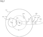
- FIG. 7 and FIG. 8 are plan views illustrating positional relationship among the top ring 116 , the eddy current sensor 210 , two optical sensors 260 and 270 and the trigger sensor 220 .
- the plurality of film thickness measuring sensors do not have to be provided at positions passing through the rotation axis C W of the top ring 116 .
- the optical sensor 270 is disposed at the polishing table 110 so as to be able to measure a film thickness of an edge of the subject to be polished 102 .
- the timing signal generator 230 can output an appropriate timing for starting measurement and an appropriate timing for finishing measurement to each of the eddy current sensor 210 , the optical sensor 260 and the optical sensor 270 using the same method as described above.
- the present embodiment it is not necessary to provide a plurality of trigger sensors 220 unlike the conventional device. Therefore, according to the present embodiment, it is possible to solve problems that the structure becomes complicated due to a plurality of trigger sensors 220 being mixed in one polishing device, that it is necessary to perform complicated rewiring, that there is a possibility of causing faulty wiring, and that it is necessary to wait for replacement parts of the trigger sensor 220 , so that it is possible to provide a film thickness measuring device having flexibility and reliability and a polishing device.
Abstract
Description
- 100 Polishing device
- 102 Subject to be polished
- 108 Polishing pad
- 110 Polishing table
- 112 First electric motor (first driving unit)
- 116 Top ring (holding unit)
- 118 Second electric motor (second driving unit)
- 200 Film thickness measuring device
- 210 Eddy current sensor
- 220 Trigger sensor
- 222 Proximity sensor
- 224 Dog
- 230 Timing signal generator
- 240 End point detector
- 250 Opposite region
- 260, 270 Optical sensor
- CT Rotation axis of polishing table 110
- CW Rotation axis of
top ring 116
Claims (22)
Applications Claiming Priority (3)
| Application Number | Priority Date | Filing Date | Title |
|---|---|---|---|
| JPJP2014-048674 | 2014-03-12 | ||
| JP2014048674A JP6423600B2 (en) | 2014-03-12 | 2014-03-12 | Film thickness measuring device and polishing device |
| JP2014-048674 | 2014-03-12 |
Publications (2)
| Publication Number | Publication Date |
|---|---|
| US20150258654A1 US20150258654A1 (en) | 2015-09-17 |
| US11065734B2 true US11065734B2 (en) | 2021-07-20 |
Family
ID=54067972
Family Applications (1)
| Application Number | Title | Priority Date | Filing Date |
|---|---|---|---|
| US14/644,501 Active 2037-05-30 US11065734B2 (en) | 2014-03-12 | 2015-03-11 | Film thickness measuring device and polishing device |
Country Status (3)
| Country | Link |
|---|---|
| US (1) | US11065734B2 (en) |
| JP (1) | JP6423600B2 (en) |
| SG (1) | SG10201501848TA (en) |
Cited By (1)
| Publication number | Priority date | Publication date | Assignee | Title |
|---|---|---|---|---|
| US11376704B2 (en) * | 2018-06-22 | 2022-07-05 | Ebara Corporation | Method of identifying trajectory of eddy current sensor, method of calculating substrate polishing progress, method of stopping operation of substrate polishing apparatus, method of regularizing substrate polishing progress, program for executing the same, and non-transitory recording medium that records program |
Families Citing this family (5)
| Publication number | Priority date | Publication date | Assignee | Title |
|---|---|---|---|---|
| JP2018001296A (en) * | 2016-06-28 | 2018-01-11 | 株式会社荏原製作所 | Polishing device, polishing method, and polishing control program |
| JP6970601B2 (en) * | 2017-12-06 | 2021-11-24 | 株式会社荏原製作所 | How to design semiconductor manufacturing equipment |
| JP7179586B2 (en) * | 2018-11-08 | 2022-11-29 | 株式会社荏原製作所 | Eddy current detection device and polishing device |
| CN111283548B (en) * | 2018-12-07 | 2023-07-18 | 株式会社迪思科 | Method for machining disc-shaped workpiece |
| CN114147622B (en) * | 2021-12-10 | 2023-04-07 | 北京晶亦精微科技股份有限公司 | CMP eddy current terminal detection device |
Citations (12)
| Publication number | Priority date | Publication date | Assignee | Title |
|---|---|---|---|---|
| US5433651A (en) | 1993-12-22 | 1995-07-18 | International Business Machines Corporation | In-situ endpoint detection and process monitoring method and apparatus for chemical-mechanical polishing |
| US5697832A (en) * | 1995-10-18 | 1997-12-16 | Cerion Technologies, Inc. | Variable speed bi-directional planetary grinding or polishing apparatus |
| WO2000026613A1 (en) | 1998-11-02 | 2000-05-11 | Applied Materials, Inc. | Optical monitoring of radial ranges in chemical mechanical polishing a metal layer on a substrate |
| US6190234B1 (en) * | 1999-01-25 | 2001-02-20 | Applied Materials, Inc. | Endpoint detection with light beams of different wavelengths |
| US6248000B1 (en) * | 1998-03-24 | 2001-06-19 | Nikon Research Corporation Of America | Polishing pad thinning to optically access a semiconductor wafer surface |
| WO2001089765A1 (en) | 2000-05-19 | 2001-11-29 | Applied Materials, Inc. | In-situ endpoint detection and process monitoring method and apparatus for chemical mechanical polishing |
| US6409576B1 (en) | 1999-07-26 | 2002-06-25 | Ebara Corporation | Polishing apparatus |
| US20040106357A1 (en) | 1995-03-28 | 2004-06-03 | Applied Materials, Inc., A Delaware Corporation | Polishing pad for in-situ endpoint detection |
| JP2004154928A (en) | 2002-10-17 | 2004-06-03 | Ebara Corp | Polishing state monitoring device, polishing device and polishing method |
| US20040259472A1 (en) | 2003-04-01 | 2004-12-23 | Chalmers Scott A. | Whole-substrate spectral imaging system for CMP |
| US20050142996A1 (en) * | 2003-04-11 | 2005-06-30 | Hisatomo Ohno | Polishing pad and method of producing same |
| JP2009233853A (en) | 2002-10-17 | 2009-10-15 | Ebara Corp | Polishing apparatus and polishing method |
-
2014
- 2014-03-12 JP JP2014048674A patent/JP6423600B2/en active Active
-
2015
- 2015-03-11 US US14/644,501 patent/US11065734B2/en active Active
- 2015-03-11 SG SG10201501848TA patent/SG10201501848TA/en unknown
Patent Citations (17)
| Publication number | Priority date | Publication date | Assignee | Title |
|---|---|---|---|---|
| JPH07235520A (en) | 1993-12-22 | 1995-09-05 | Internatl Business Mach Corp <Ibm> | Grind process monitoring device and its monitor method |
| US5433651A (en) | 1993-12-22 | 1995-07-18 | International Business Machines Corporation | In-situ endpoint detection and process monitoring method and apparatus for chemical-mechanical polishing |
| US20040106357A1 (en) | 1995-03-28 | 2004-06-03 | Applied Materials, Inc., A Delaware Corporation | Polishing pad for in-situ endpoint detection |
| US5697832A (en) * | 1995-10-18 | 1997-12-16 | Cerion Technologies, Inc. | Variable speed bi-directional planetary grinding or polishing apparatus |
| US6248000B1 (en) * | 1998-03-24 | 2001-06-19 | Nikon Research Corporation Of America | Polishing pad thinning to optically access a semiconductor wafer surface |
| JP2002529686A (en) | 1998-11-02 | 2002-09-10 | アプライド マテリアルズ インコーポレイテッド | Optical monitoring of radial range in chemical mechanical polishing of metal layer on substrate |
| WO2000026613A1 (en) | 1998-11-02 | 2000-05-11 | Applied Materials, Inc. | Optical monitoring of radial ranges in chemical mechanical polishing a metal layer on a substrate |
| US6190234B1 (en) * | 1999-01-25 | 2001-02-20 | Applied Materials, Inc. | Endpoint detection with light beams of different wavelengths |
| US6409576B1 (en) | 1999-07-26 | 2002-06-25 | Ebara Corporation | Polishing apparatus |
| JP2003534649A (en) | 2000-05-19 | 2003-11-18 | アプライド マテリアルズ インコーポレイテッド | Method and apparatus for on-site endpoint detection and process monitoring for chemical mechanical polishing |
| WO2001089765A1 (en) | 2000-05-19 | 2001-11-29 | Applied Materials, Inc. | In-situ endpoint detection and process monitoring method and apparatus for chemical mechanical polishing |
| JP2004154928A (en) | 2002-10-17 | 2004-06-03 | Ebara Corp | Polishing state monitoring device, polishing device and polishing method |
| US20060166606A1 (en) * | 2002-10-17 | 2006-07-27 | Yoichi Kobayashi | Polishing state monitoring apparatus and polishing apparatus and method |
| US7252575B2 (en) * | 2002-10-17 | 2007-08-07 | Ebara Corporation | Polishing state monitoring apparatus and polishing apparatus and method |
| JP2009233853A (en) | 2002-10-17 | 2009-10-15 | Ebara Corp | Polishing apparatus and polishing method |
| US20040259472A1 (en) | 2003-04-01 | 2004-12-23 | Chalmers Scott A. | Whole-substrate spectral imaging system for CMP |
| US20050142996A1 (en) * | 2003-04-11 | 2005-06-30 | Hisatomo Ohno | Polishing pad and method of producing same |
Non-Patent Citations (2)
| Title |
|---|
| Japanese Office Action No. 2014-048674 dated Dec. 19, 2017. |
| Singapore Office Action issued in Singapore Patent Application No. 10201501848T dated Jul. 17, 2017. |
Cited By (1)
| Publication number | Priority date | Publication date | Assignee | Title |
|---|---|---|---|---|
| US11376704B2 (en) * | 2018-06-22 | 2022-07-05 | Ebara Corporation | Method of identifying trajectory of eddy current sensor, method of calculating substrate polishing progress, method of stopping operation of substrate polishing apparatus, method of regularizing substrate polishing progress, program for executing the same, and non-transitory recording medium that records program |
Also Published As
| Publication number | Publication date |
|---|---|
| SG10201501848TA (en) | 2015-10-29 |
| JP2015171744A (en) | 2015-10-01 |
| JP6423600B2 (en) | 2018-11-14 |
| US20150258654A1 (en) | 2015-09-17 |
Similar Documents
| Publication | Publication Date | Title |
|---|---|---|
| US11065734B2 (en) | Film thickness measuring device and polishing device | |
| US9555517B2 (en) | Film thickness signal processing apparatus, polishing apparatus, film thickness signal processing method, and polishing method | |
| CN104907920B (en) | Correction method, film thickness retriever and the eddy current sensor of film thickness measuring value | |
| KR101597158B1 (en) | Method and apparatus for polishing work | |
| US10569380B2 (en) | Film thickness signal processing apparatus, and polishing apparatus | |
| JP4790475B2 (en) | Polishing apparatus, polishing method, and substrate film thickness measurement program | |
| US6930478B2 (en) | Method for monitoring a metal layer during chemical mechanical polishing using a phase difference signal | |
| KR101725595B1 (en) | Polishing method | |
| US8284560B2 (en) | Eddy current sensor with enhanced edge resolution | |
| JP6618822B2 (en) | Method for detecting wear amount of grinding wheel | |
| KR20160052216A (en) | Chemical mechanical polishing apparatus and method of measuring wafer metal layer thickness using same | |
| US20210199415A1 (en) | Output signal processing circuit for eddy current sensor and output signal processing method for eddy current sensor | |
| US10625390B2 (en) | Polishing apparatus and polishing method | |
| US9524913B2 (en) | Polishing method and polishing apparatus | |
| JP6219692B2 (en) | Wafer ID mark reader | |
| JP7430872B2 (en) | Conveyance method and conveyance device | |
| JP2016064459A (en) | Method of grinding workpiece | |
| JP6445241B2 (en) | Eddy current sensor | |
| JP2015172536A (en) | Film thickness measurement value correction method and film thickness corrector | |
| JP2005034992A (en) | Detection method of polishing endpoint | |
| WO2023162478A1 (en) | Polishing device and method for detecting polishing end point in polishing device | |
| JP2015195268A (en) | Polishing progress estimation method and polishing progress estimation device | |
| KR200471467Y1 (en) | Apparatus for detecting rotation of pad conditioner | |
| JP2020072172A (en) | Grinding machine | |
| JP2020138264A (en) | Polishing device, polishing method, and memory medium storing program |
Legal Events
| Date | Code | Title | Description |
|---|---|---|---|
| AS | Assignment |
Owner name: EBARA CORPORATION, JAPAN Free format text: ASSIGNMENT OF ASSIGNORS INTEREST;ASSIGNOR:SHINOZAKI, HIROYUKI;REEL/FRAME:035147/0681 Effective date: 20141223 |
|
| STPP | Information on status: patent application and granting procedure in general |
Free format text: FINAL REJECTION MAILED |
|
| STPP | Information on status: patent application and granting procedure in general |
Free format text: DOCKETED NEW CASE - READY FOR EXAMINATION |
|
| STPP | Information on status: patent application and granting procedure in general |
Free format text: NON FINAL ACTION MAILED |
|
| STPP | Information on status: patent application and granting procedure in general |
Free format text: RESPONSE TO NON-FINAL OFFICE ACTION ENTERED AND FORWARDED TO EXAMINER |
|
| STPP | Information on status: patent application and granting procedure in general |
Free format text: NON FINAL ACTION MAILED |
|
| STPP | Information on status: patent application and granting procedure in general |
Free format text: RESPONSE TO NON-FINAL OFFICE ACTION ENTERED AND FORWARDED TO EXAMINER |
|
| STCV | Information on status: appeal procedure |
Free format text: NOTICE OF APPEAL FILED |
|
| STCV | Information on status: appeal procedure |
Free format text: APPEAL BRIEF (OR SUPPLEMENTAL BRIEF) ENTERED AND FORWARDED TO EXAMINER |
|
| STPP | Information on status: patent application and granting procedure in general |
Free format text: NOTICE OF ALLOWANCE MAILED -- APPLICATION RECEIVED IN OFFICE OF PUBLICATIONS |
|
| STPP | Information on status: patent application and granting procedure in general |
Free format text: PUBLICATIONS -- ISSUE FEE PAYMENT RECEIVED |
|
| STPP | Information on status: patent application and granting procedure in general |
Free format text: PUBLICATIONS -- ISSUE FEE PAYMENT VERIFIED |
|
| STCF | Information on status: patent grant |
Free format text: PATENTED CASE |