US11064276B2 - Panel bottom member and display device including the same - Google Patents
Panel bottom member and display device including the same Download PDFInfo
- Publication number
- US11064276B2 US11064276B2 US15/941,572 US201815941572A US11064276B2 US 11064276 B2 US11064276 B2 US 11064276B2 US 201815941572 A US201815941572 A US 201815941572A US 11064276 B2 US11064276 B2 US 11064276B2
- Authority
- US
- United States
- Prior art keywords
- layer
- light absorbing
- vibration sound
- heat dissipation
- sound element
- Prior art date
- Legal status (The legal status is an assumption and is not a legal conclusion. Google has not performed a legal analysis and makes no representation as to the accuracy of the status listed.)
- Active
Links
- 239000010410 layer Substances 0.000 claims abstract description 253
- 239000011229 interlayer Substances 0.000 claims abstract description 47
- 230000017525 heat dissipation Effects 0.000 claims description 60
- 239000000463 material Substances 0.000 claims description 53
- 239000000758 substrate Substances 0.000 claims description 34
- 238000005538 encapsulation Methods 0.000 claims description 11
- 230000004044 response Effects 0.000 claims description 8
- 230000005236 sound signal Effects 0.000 claims description 8
- 239000002861 polymer material Substances 0.000 claims description 4
- 229920001746 electroactive polymer Polymers 0.000 claims description 3
- 239000011368 organic material Substances 0.000 claims description 3
- 239000010408 film Substances 0.000 description 47
- 230000004048 modification Effects 0.000 description 24
- 238000012986 modification Methods 0.000 description 24
- 239000002346 layers by function Substances 0.000 description 18
- 238000010586 diagram Methods 0.000 description 10
- 238000000034 method Methods 0.000 description 9
- 229920000642 polymer Polymers 0.000 description 7
- 239000004417 polycarbonate Substances 0.000 description 6
- 230000008569 process Effects 0.000 description 6
- 230000008901 benefit Effects 0.000 description 5
- 230000005540 biological transmission Effects 0.000 description 5
- 230000000694 effects Effects 0.000 description 5
- -1 hafnium nitride Chemical class 0.000 description 5
- RYGMFSIKBFXOCR-UHFFFAOYSA-N Copper Chemical compound [Cu] RYGMFSIKBFXOCR-UHFFFAOYSA-N 0.000 description 4
- PXHVJJICTQNCMI-UHFFFAOYSA-N Nickel Chemical compound [Ni] PXHVJJICTQNCMI-UHFFFAOYSA-N 0.000 description 4
- 229910052802 copper Inorganic materials 0.000 description 4
- 239000010949 copper Substances 0.000 description 4
- 238000000151 deposition Methods 0.000 description 4
- 230000005684 electric field Effects 0.000 description 4
- 229920000139 polyethylene terephthalate Polymers 0.000 description 4
- 239000005020 polyethylene terephthalate Substances 0.000 description 4
- 239000011347 resin Substances 0.000 description 4
- 229920005989 resin Polymers 0.000 description 4
- OKTJSMMVPCPJKN-UHFFFAOYSA-N Carbon Chemical compound [C] OKTJSMMVPCPJKN-UHFFFAOYSA-N 0.000 description 3
- 239000002033 PVDF binder Substances 0.000 description 3
- 239000004698 Polyethylene Substances 0.000 description 3
- 239000004743 Polypropylene Substances 0.000 description 3
- 239000004020 conductor Substances 0.000 description 3
- 230000008602 contraction Effects 0.000 description 3
- 239000011810 insulating material Substances 0.000 description 3
- 238000005259 measurement Methods 0.000 description 3
- 229910052751 metal Inorganic materials 0.000 description 3
- 239000002184 metal Substances 0.000 description 3
- 238000000059 patterning Methods 0.000 description 3
- 229920002981 polyvinylidene fluoride Polymers 0.000 description 3
- 239000002096 quantum dot Substances 0.000 description 3
- 239000010409 thin film Substances 0.000 description 3
- 229920008347 Cellulose acetate propionate Polymers 0.000 description 2
- 229920002284 Cellulose triacetate Polymers 0.000 description 2
- JOYRKODLDBILNP-UHFFFAOYSA-N Ethyl urethane Chemical compound CCOC(N)=O JOYRKODLDBILNP-UHFFFAOYSA-N 0.000 description 2
- 239000004697 Polyetherimide Substances 0.000 description 2
- 239000004734 Polyphenylene sulfide Substances 0.000 description 2
- NNLVGZFZQQXQNW-ADJNRHBOSA-N [(2r,3r,4s,5r,6s)-4,5-diacetyloxy-3-[(2s,3r,4s,5r,6r)-3,4,5-triacetyloxy-6-(acetyloxymethyl)oxan-2-yl]oxy-6-[(2r,3r,4s,5r,6s)-4,5,6-triacetyloxy-2-(acetyloxymethyl)oxan-3-yl]oxyoxan-2-yl]methyl acetate Chemical compound O([C@@H]1O[C@@H]([C@H]([C@H](OC(C)=O)[C@H]1OC(C)=O)O[C@H]1[C@@H]([C@@H](OC(C)=O)[C@H](OC(C)=O)[C@@H](COC(C)=O)O1)OC(C)=O)COC(=O)C)[C@@H]1[C@@H](COC(C)=O)O[C@@H](OC(C)=O)[C@H](OC(C)=O)[C@H]1OC(C)=O NNLVGZFZQQXQNW-ADJNRHBOSA-N 0.000 description 2
- 239000000853 adhesive Substances 0.000 description 2
- 230000001070 adhesive effect Effects 0.000 description 2
- 239000002041 carbon nanotube Substances 0.000 description 2
- 229910021393 carbon nanotube Inorganic materials 0.000 description 2
- 239000011248 coating agent Substances 0.000 description 2
- 238000000576 coating method Methods 0.000 description 2
- 238000007667 floating Methods 0.000 description 2
- 239000011521 glass Substances 0.000 description 2
- 229910052451 lead zirconate titanate Inorganic materials 0.000 description 2
- 238000004519 manufacturing process Methods 0.000 description 2
- 239000007769 metal material Substances 0.000 description 2
- 229910052759 nickel Inorganic materials 0.000 description 2
- 230000003287 optical effect Effects 0.000 description 2
- 239000012994 photoredox catalyst Substances 0.000 description 2
- 229920003207 poly(ethylene-2,6-naphthalate) Polymers 0.000 description 2
- 229920003229 poly(methyl methacrylate) Polymers 0.000 description 2
- 229920000058 polyacrylate Polymers 0.000 description 2
- 229920000515 polycarbonate Polymers 0.000 description 2
- 229920000728 polyester Polymers 0.000 description 2
- 229920001601 polyetherimide Polymers 0.000 description 2
- 229920000573 polyethylene Polymers 0.000 description 2
- 239000011112 polyethylene naphthalate Substances 0.000 description 2
- 239000004926 polymethyl methacrylate Substances 0.000 description 2
- 229920000069 polyphenylene sulfide Polymers 0.000 description 2
- 229920001155 polypropylene Polymers 0.000 description 2
- 238000007639 printing Methods 0.000 description 2
- 230000035939 shock Effects 0.000 description 2
- 229910052709 silver Inorganic materials 0.000 description 2
- 239000004332 silver Substances 0.000 description 2
- 239000002356 single layer Substances 0.000 description 2
- 229920003002 synthetic resin Polymers 0.000 description 2
- 229920002554 vinyl polymer Polymers 0.000 description 2
- 239000004925 Acrylic resin Substances 0.000 description 1
- 229920000178 Acrylic resin Polymers 0.000 description 1
- 229920000089 Cyclic olefin copolymer Polymers 0.000 description 1
- 108010010803 Gelatin Proteins 0.000 description 1
- 239000004642 Polyimide Substances 0.000 description 1
- 229910052581 Si3N4 Inorganic materials 0.000 description 1
- VYPSYNLAJGMNEJ-UHFFFAOYSA-N Silicium dioxide Chemical compound O=[Si]=O VYPSYNLAJGMNEJ-UHFFFAOYSA-N 0.000 description 1
- XUIMIQQOPSSXEZ-UHFFFAOYSA-N Silicon Chemical compound [Si] XUIMIQQOPSSXEZ-UHFFFAOYSA-N 0.000 description 1
- BQCADISMDOOEFD-UHFFFAOYSA-N Silver Chemical compound [Ag] BQCADISMDOOEFD-UHFFFAOYSA-N 0.000 description 1
- GWEVSGVZZGPLCZ-UHFFFAOYSA-N Titan oxide Chemical compound O=[Ti]=O GWEVSGVZZGPLCZ-UHFFFAOYSA-N 0.000 description 1
- NRTOMJZYCJJWKI-UHFFFAOYSA-N Titanium nitride Chemical compound [Ti]#N NRTOMJZYCJJWKI-UHFFFAOYSA-N 0.000 description 1
- 239000011358 absorbing material Substances 0.000 description 1
- NIXOWILDQLNWCW-UHFFFAOYSA-N acrylic acid group Chemical group C(C=C)(=O)O NIXOWILDQLNWCW-UHFFFAOYSA-N 0.000 description 1
- 239000012790 adhesive layer Substances 0.000 description 1
- 230000002411 adverse Effects 0.000 description 1
- QVGXLLKOCUKJST-UHFFFAOYSA-N atomic oxygen Chemical compound [O] QVGXLLKOCUKJST-UHFFFAOYSA-N 0.000 description 1
- 230000003139 buffering effect Effects 0.000 description 1
- 239000012461 cellulose resin Substances 0.000 description 1
- 239000000919 ceramic Substances 0.000 description 1
- 229910000420 cerium oxide Inorganic materials 0.000 description 1
- 239000011247 coating layer Substances 0.000 description 1
- 230000000295 complement effect Effects 0.000 description 1
- 239000002322 conducting polymer Substances 0.000 description 1
- 229920001940 conductive polymer Polymers 0.000 description 1
- PMHQVHHXPFUNSP-UHFFFAOYSA-M copper(1+);methylsulfanylmethane;bromide Chemical compound Br[Cu].CSC PMHQVHHXPFUNSP-UHFFFAOYSA-M 0.000 description 1
- 230000008878 coupling Effects 0.000 description 1
- 238000010168 coupling process Methods 0.000 description 1
- 238000005859 coupling reaction Methods 0.000 description 1
- 230000008021 deposition Effects 0.000 description 1
- 238000006073 displacement reaction Methods 0.000 description 1
- 229920001971 elastomer Polymers 0.000 description 1
- 239000003822 epoxy resin Substances 0.000 description 1
- 238000005187 foaming Methods 0.000 description 1
- 229920000159 gelatin Polymers 0.000 description 1
- 239000008273 gelatin Substances 0.000 description 1
- 235000019322 gelatine Nutrition 0.000 description 1
- 235000011852 gelatine desserts Nutrition 0.000 description 1
- 229910002804 graphite Inorganic materials 0.000 description 1
- 239000010439 graphite Substances 0.000 description 1
- 229910052735 hafnium Inorganic materials 0.000 description 1
- 238000010438 heat treatment Methods 0.000 description 1
- AMGQUBHHOARCQH-UHFFFAOYSA-N indium;oxotin Chemical compound [In].[Sn]=O AMGQUBHHOARCQH-UHFFFAOYSA-N 0.000 description 1
- 238000009812 interlayer coupling reaction Methods 0.000 description 1
- 239000012948 isocyanate Substances 0.000 description 1
- 150000002513 isocyanates Chemical class 0.000 description 1
- 239000004816 latex Substances 0.000 description 1
- 229920000126 latex Polymers 0.000 description 1
- HFGPZNIAWCZYJU-UHFFFAOYSA-N lead zirconate titanate Chemical compound [O-2].[O-2].[O-2].[O-2].[O-2].[Ti+4].[Zr+4].[Pb+2] HFGPZNIAWCZYJU-UHFFFAOYSA-N 0.000 description 1
- 230000000670 limiting effect Effects 0.000 description 1
- 239000007788 liquid Substances 0.000 description 1
- 239000004973 liquid crystal related substance Substances 0.000 description 1
- 230000000873 masking effect Effects 0.000 description 1
- 239000012528 membrane Substances 0.000 description 1
- 239000000113 methacrylic resin Substances 0.000 description 1
- 238000000465 moulding Methods 0.000 description 1
- 230000001151 other effect Effects 0.000 description 1
- TWNQGVIAIRXVLR-UHFFFAOYSA-N oxo(oxoalumanyloxy)alumane Chemical compound O=[Al]O[Al]=O TWNQGVIAIRXVLR-UHFFFAOYSA-N 0.000 description 1
- BMMGVYCKOGBVEV-UHFFFAOYSA-N oxo(oxoceriooxy)cerium Chemical compound [Ce]=O.O=[Ce]=O BMMGVYCKOGBVEV-UHFFFAOYSA-N 0.000 description 1
- 229910052760 oxygen Inorganic materials 0.000 description 1
- 239000001301 oxygen Substances 0.000 description 1
- 230000036961 partial effect Effects 0.000 description 1
- 230000000149 penetrating effect Effects 0.000 description 1
- 125000002080 perylenyl group Chemical group C1(=CC=C2C=CC=C3C4=CC=CC5=CC=CC(C1=C23)=C45)* 0.000 description 1
- CSHWQDPOILHKBI-UHFFFAOYSA-N peryrene Natural products C1=CC(C2=CC=CC=3C2=C2C=CC=3)=C3C2=CC=CC3=C1 CSHWQDPOILHKBI-UHFFFAOYSA-N 0.000 description 1
- 239000000049 pigment Substances 0.000 description 1
- 229920003023 plastic Polymers 0.000 description 1
- 239000004033 plastic Substances 0.000 description 1
- 229920002492 poly(sulfone) Polymers 0.000 description 1
- 229920001230 polyarylate Polymers 0.000 description 1
- 229920000647 polyepoxide Polymers 0.000 description 1
- 229920001721 polyimide Polymers 0.000 description 1
- 229920001195 polyisoprene Polymers 0.000 description 1
- 239000002952 polymeric resin Substances 0.000 description 1
- 229920001296 polysiloxane Polymers 0.000 description 1
- 229920002635 polyurethane Polymers 0.000 description 1
- 239000004814 polyurethane Substances 0.000 description 1
- 229920002451 polyvinyl alcohol Polymers 0.000 description 1
- 230000002829 reductive effect Effects 0.000 description 1
- 238000002310 reflectometry Methods 0.000 description 1
- 239000010980 sapphire Substances 0.000 description 1
- 229910052594 sapphire Inorganic materials 0.000 description 1
- 229910052710 silicon Inorganic materials 0.000 description 1
- 239000010703 silicon Substances 0.000 description 1
- HQVNEWCFYHHQES-UHFFFAOYSA-N silicon nitride Chemical compound N12[Si]34N5[Si]62N3[Si]51N64 HQVNEWCFYHHQES-UHFFFAOYSA-N 0.000 description 1
- 229910052814 silicon oxide Inorganic materials 0.000 description 1
- 229920005573 silicon-containing polymer Polymers 0.000 description 1
- 229920002050 silicone resin Polymers 0.000 description 1
- 239000000057 synthetic resin Substances 0.000 description 1
- MZLGASXMSKOWSE-UHFFFAOYSA-N tantalum nitride Chemical compound [Ta]#N MZLGASXMSKOWSE-UHFFFAOYSA-N 0.000 description 1
- 229920002803 thermoplastic polyurethane Polymers 0.000 description 1
- XOLBLPGZBRYERU-UHFFFAOYSA-N tin dioxide Chemical compound O=[Sn]=O XOLBLPGZBRYERU-UHFFFAOYSA-N 0.000 description 1
- 229910001887 tin oxide Inorganic materials 0.000 description 1
- OGIDPMRJRNCKJF-UHFFFAOYSA-N titanium oxide Inorganic materials [Ti]=O OGIDPMRJRNCKJF-UHFFFAOYSA-N 0.000 description 1
- WFKWXMTUELFFGS-UHFFFAOYSA-N tungsten Chemical compound [W] WFKWXMTUELFFGS-UHFFFAOYSA-N 0.000 description 1
- 229910052721 tungsten Inorganic materials 0.000 description 1
- 239000010937 tungsten Substances 0.000 description 1
- 125000000391 vinyl group Chemical group [H]C([*])=C([H])[H] 0.000 description 1
- XLYOFNOQVPJJNP-UHFFFAOYSA-N water Substances O XLYOFNOQVPJJNP-UHFFFAOYSA-N 0.000 description 1
- YVTHLONGBIQYBO-UHFFFAOYSA-N zinc indium(3+) oxygen(2-) Chemical compound [O--].[Zn++].[In+3] YVTHLONGBIQYBO-UHFFFAOYSA-N 0.000 description 1
- ZVWKZXLXHLZXLS-UHFFFAOYSA-N zirconium nitride Chemical compound [Zr]#N ZVWKZXLXHLZXLS-UHFFFAOYSA-N 0.000 description 1
- 229910000859 α-Fe Inorganic materials 0.000 description 1
Images


Classifications
-
- H—ELECTRICITY
- H05—ELECTRIC TECHNIQUES NOT OTHERWISE PROVIDED FOR
- H05K—PRINTED CIRCUITS; CASINGS OR CONSTRUCTIONAL DETAILS OF ELECTRIC APPARATUS; MANUFACTURE OF ASSEMBLAGES OF ELECTRICAL COMPONENTS
- H05K7/00—Constructional details common to different types of electric apparatus
- H05K7/20—Modifications to facilitate cooling, ventilating, or heating
- H05K7/20954—Modifications to facilitate cooling, ventilating, or heating for display panels
- H05K7/20963—Heat transfer by conduction from internal heat source to heat radiating structure
-
- H—ELECTRICITY
- H04—ELECTRIC COMMUNICATION TECHNIQUE
- H04R—LOUDSPEAKERS, MICROPHONES, GRAMOPHONE PICK-UPS OR LIKE ACOUSTIC ELECTROMECHANICAL TRANSDUCERS; DEAF-AID SETS; PUBLIC ADDRESS SYSTEMS
- H04R1/00—Details of transducers, loudspeakers or microphones
- H04R1/02—Casings; Cabinets ; Supports therefor; Mountings therein
- H04R1/028—Casings; Cabinets ; Supports therefor; Mountings therein associated with devices performing functions other than acoustics, e.g. electric candles
-
- H—ELECTRICITY
- H10—SEMICONDUCTOR DEVICES; ELECTRIC SOLID-STATE DEVICES NOT OTHERWISE PROVIDED FOR
- H10K—ORGANIC ELECTRIC SOLID-STATE DEVICES
- H10K71/00—Manufacture or treatment specially adapted for the organic devices covered by this subclass
-
- H—ELECTRICITY
- H04—ELECTRIC COMMUNICATION TECHNIQUE
- H04R—LOUDSPEAKERS, MICROPHONES, GRAMOPHONE PICK-UPS OR LIKE ACOUSTIC ELECTROMECHANICAL TRANSDUCERS; DEAF-AID SETS; PUBLIC ADDRESS SYSTEMS
- H04R9/00—Transducers of moving-coil, moving-strip, or moving-wire type
- H04R9/06—Loudspeakers
-
- G—PHYSICS
- G09—EDUCATION; CRYPTOGRAPHY; DISPLAY; ADVERTISING; SEALS
- G09F—DISPLAYING; ADVERTISING; SIGNS; LABELS OR NAME-PLATES; SEALS
- G09F9/00—Indicating arrangements for variable information in which the information is built-up on a support by selection or combination of individual elements
-
- H01L27/3225—
-
- H01L51/524—
-
- H01L51/5253—
-
- H01L51/5281—
-
- H01L51/529—
-
- H—ELECTRICITY
- H04—ELECTRIC COMMUNICATION TECHNIQUE
- H04R—LOUDSPEAKERS, MICROPHONES, GRAMOPHONE PICK-UPS OR LIKE ACOUSTIC ELECTROMECHANICAL TRANSDUCERS; DEAF-AID SETS; PUBLIC ADDRESS SYSTEMS
- H04R17/00—Piezoelectric transducers; Electrostrictive transducers
-
- H—ELECTRICITY
- H04—ELECTRIC COMMUNICATION TECHNIQUE
- H04R—LOUDSPEAKERS, MICROPHONES, GRAMOPHONE PICK-UPS OR LIKE ACOUSTIC ELECTROMECHANICAL TRANSDUCERS; DEAF-AID SETS; PUBLIC ADDRESS SYSTEMS
- H04R7/00—Diaphragms for electromechanical transducers; Cones
- H04R7/02—Diaphragms for electromechanical transducers; Cones characterised by the construction
- H04R7/04—Plane diaphragms
-
- H—ELECTRICITY
- H04—ELECTRIC COMMUNICATION TECHNIQUE
- H04R—LOUDSPEAKERS, MICROPHONES, GRAMOPHONE PICK-UPS OR LIKE ACOUSTIC ELECTROMECHANICAL TRANSDUCERS; DEAF-AID SETS; PUBLIC ADDRESS SYSTEMS
- H04R9/00—Transducers of moving-coil, moving-strip, or moving-wire type
- H04R9/02—Details
-
- H—ELECTRICITY
- H05—ELECTRIC TECHNIQUES NOT OTHERWISE PROVIDED FOR
- H05K—PRINTED CIRCUITS; CASINGS OR CONSTRUCTIONAL DETAILS OF ELECTRIC APPARATUS; MANUFACTURE OF ASSEMBLAGES OF ELECTRICAL COMPONENTS
- H05K5/00—Casings, cabinets or drawers for electric apparatus
- H05K5/0017—Casings, cabinets or drawers for electric apparatus with operator interface units
-
- H—ELECTRICITY
- H05—ELECTRIC TECHNIQUES NOT OTHERWISE PROVIDED FOR
- H05K—PRINTED CIRCUITS; CASINGS OR CONSTRUCTIONAL DETAILS OF ELECTRIC APPARATUS; MANUFACTURE OF ASSEMBLAGES OF ELECTRICAL COMPONENTS
- H05K9/00—Screening of apparatus or components against electric or magnetic fields
- H05K9/0007—Casings
- H05K9/0054—Casings specially adapted for display applications
-
- H—ELECTRICITY
- H10—SEMICONDUCTOR DEVICES; ELECTRIC SOLID-STATE DEVICES NOT OTHERWISE PROVIDED FOR
- H10K—ORGANIC ELECTRIC SOLID-STATE DEVICES
- H10K50/00—Organic light-emitting devices
- H10K50/80—Constructional details
- H10K50/84—Passivation; Containers; Encapsulations
- H10K50/841—Self-supporting sealing arrangements
-
- H—ELECTRICITY
- H10—SEMICONDUCTOR DEVICES; ELECTRIC SOLID-STATE DEVICES NOT OTHERWISE PROVIDED FOR
- H10K—ORGANIC ELECTRIC SOLID-STATE DEVICES
- H10K50/00—Organic light-emitting devices
- H10K50/80—Constructional details
- H10K50/84—Passivation; Containers; Encapsulations
- H10K50/844—Encapsulations
-
- H—ELECTRICITY
- H10—SEMICONDUCTOR DEVICES; ELECTRIC SOLID-STATE DEVICES NOT OTHERWISE PROVIDED FOR
- H10K—ORGANIC ELECTRIC SOLID-STATE DEVICES
- H10K50/00—Organic light-emitting devices
- H10K50/80—Constructional details
- H10K50/86—Arrangements for improving contrast, e.g. preventing reflection of ambient light
- H10K50/865—Arrangements for improving contrast, e.g. preventing reflection of ambient light comprising light absorbing layers, e.g. light-blocking layers
-
- H—ELECTRICITY
- H10—SEMICONDUCTOR DEVICES; ELECTRIC SOLID-STATE DEVICES NOT OTHERWISE PROVIDED FOR
- H10K—ORGANIC ELECTRIC SOLID-STATE DEVICES
- H10K50/00—Organic light-emitting devices
- H10K50/80—Constructional details
- H10K50/87—Arrangements for heating or cooling
-
- H—ELECTRICITY
- H10—SEMICONDUCTOR DEVICES; ELECTRIC SOLID-STATE DEVICES NOT OTHERWISE PROVIDED FOR
- H10K—ORGANIC ELECTRIC SOLID-STATE DEVICES
- H10K59/00—Integrated devices, or assemblies of multiple devices, comprising at least one organic light-emitting element covered by group H10K50/00
-
- H—ELECTRICITY
- H10—SEMICONDUCTOR DEVICES; ELECTRIC SOLID-STATE DEVICES NOT OTHERWISE PROVIDED FOR
- H10K—ORGANIC ELECTRIC SOLID-STATE DEVICES
- H10K77/00—Constructional details of devices covered by this subclass and not covered by groups H10K10/80, H10K30/80, H10K50/80 or H10K59/80
- H10K77/10—Substrates, e.g. flexible substrates
-
- H—ELECTRICITY
- H10—SEMICONDUCTOR DEVICES; ELECTRIC SOLID-STATE DEVICES NOT OTHERWISE PROVIDED FOR
- H10N—ELECTRIC SOLID-STATE DEVICES NOT OTHERWISE PROVIDED FOR
- H10N30/00—Piezoelectric or electrostrictive devices
- H10N30/01—Manufacture or treatment
- H10N30/04—Treatments to modify a piezoelectric or electrostrictive property, e.g. polarisation characteristics, vibration characteristics or mode tuning
-
- H—ELECTRICITY
- H10—SEMICONDUCTOR DEVICES; ELECTRIC SOLID-STATE DEVICES NOT OTHERWISE PROVIDED FOR
- H10N—ELECTRIC SOLID-STATE DEVICES NOT OTHERWISE PROVIDED FOR
- H10N30/00—Piezoelectric or electrostrictive devices
- H10N30/20—Piezoelectric or electrostrictive devices with electrical input and mechanical output, e.g. functioning as actuators or vibrators
-
- H01L2251/5338—
-
- H01L27/323—
-
- H01L51/0097—
-
- H—ELECTRICITY
- H04—ELECTRIC COMMUNICATION TECHNIQUE
- H04R—LOUDSPEAKERS, MICROPHONES, GRAMOPHONE PICK-UPS OR LIKE ACOUSTIC ELECTROMECHANICAL TRANSDUCERS; DEAF-AID SETS; PUBLIC ADDRESS SYSTEMS
- H04R2400/00—Loudspeakers
- H04R2400/11—Aspects regarding the frame of loudspeaker transducers
-
- H—ELECTRICITY
- H04—ELECTRIC COMMUNICATION TECHNIQUE
- H04R—LOUDSPEAKERS, MICROPHONES, GRAMOPHONE PICK-UPS OR LIKE ACOUSTIC ELECTROMECHANICAL TRANSDUCERS; DEAF-AID SETS; PUBLIC ADDRESS SYSTEMS
- H04R2499/00—Aspects covered by H04R or H04S not otherwise provided for in their subgroups
- H04R2499/10—General applications
- H04R2499/15—Transducers incorporated in visual displaying devices, e.g. televisions, computer displays, laptops
-
- H—ELECTRICITY
- H04—ELECTRIC COMMUNICATION TECHNIQUE
- H04R—LOUDSPEAKERS, MICROPHONES, GRAMOPHONE PICK-UPS OR LIKE ACOUSTIC ELECTROMECHANICAL TRANSDUCERS; DEAF-AID SETS; PUBLIC ADDRESS SYSTEMS
- H04R7/00—Diaphragms for electromechanical transducers; Cones
- H04R7/02—Diaphragms for electromechanical transducers; Cones characterised by the construction
- H04R7/04—Plane diaphragms
- H04R7/045—Plane diaphragms using the distributed mode principle, i.e. whereby the acoustic radiation is emanated from uniformly distributed free bending wave vibration induced in a stiff panel and not from pistonic motion
-
- H—ELECTRICITY
- H04—ELECTRIC COMMUNICATION TECHNIQUE
- H04R—LOUDSPEAKERS, MICROPHONES, GRAMOPHONE PICK-UPS OR LIKE ACOUSTIC ELECTROMECHANICAL TRANSDUCERS; DEAF-AID SETS; PUBLIC ADDRESS SYSTEMS
- H04R7/00—Diaphragms for electromechanical transducers; Cones
- H04R7/02—Diaphragms for electromechanical transducers; Cones characterised by the construction
- H04R7/04—Plane diaphragms
- H04R7/06—Plane diaphragms comprising a plurality of sections or layers
-
- H—ELECTRICITY
- H04—ELECTRIC COMMUNICATION TECHNIQUE
- H04R—LOUDSPEAKERS, MICROPHONES, GRAMOPHONE PICK-UPS OR LIKE ACOUSTIC ELECTROMECHANICAL TRANSDUCERS; DEAF-AID SETS; PUBLIC ADDRESS SYSTEMS
- H04R7/00—Diaphragms for electromechanical transducers; Cones
- H04R7/16—Mounting or tensioning of diaphragms or cones
-
- H—ELECTRICITY
- H10—SEMICONDUCTOR DEVICES; ELECTRIC SOLID-STATE DEVICES NOT OTHERWISE PROVIDED FOR
- H10K—ORGANIC ELECTRIC SOLID-STATE DEVICES
- H10K2102/00—Constructional details relating to the organic devices covered by this subclass
- H10K2102/301—Details of OLEDs
- H10K2102/311—Flexible OLED
-
- H—ELECTRICITY
- H10—SEMICONDUCTOR DEVICES; ELECTRIC SOLID-STATE DEVICES NOT OTHERWISE PROVIDED FOR
- H10K—ORGANIC ELECTRIC SOLID-STATE DEVICES
- H10K59/00—Integrated devices, or assemblies of multiple devices, comprising at least one organic light-emitting element covered by group H10K50/00
- H10K59/40—OLEDs integrated with touch screens
-
- H—ELECTRICITY
- H10—SEMICONDUCTOR DEVICES; ELECTRIC SOLID-STATE DEVICES NOT OTHERWISE PROVIDED FOR
- H10K—ORGANIC ELECTRIC SOLID-STATE DEVICES
- H10K77/00—Constructional details of devices covered by this subclass and not covered by groups H10K10/80, H10K30/80, H10K50/80 or H10K59/80
- H10K77/10—Substrates, e.g. flexible substrates
- H10K77/111—Flexible substrates
-
- Y—GENERAL TAGGING OF NEW TECHNOLOGICAL DEVELOPMENTS; GENERAL TAGGING OF CROSS-SECTIONAL TECHNOLOGIES SPANNING OVER SEVERAL SECTIONS OF THE IPC; TECHNICAL SUBJECTS COVERED BY FORMER USPC CROSS-REFERENCE ART COLLECTIONS [XRACs] AND DIGESTS
- Y02—TECHNOLOGIES OR APPLICATIONS FOR MITIGATION OR ADAPTATION AGAINST CLIMATE CHANGE
- Y02E—REDUCTION OF GREENHOUSE GAS [GHG] EMISSIONS, RELATED TO ENERGY GENERATION, TRANSMISSION OR DISTRIBUTION
- Y02E10/00—Energy generation through renewable energy sources
- Y02E10/50—Photovoltaic [PV] energy
- Y02E10/549—Organic PV cells
-
- Y—GENERAL TAGGING OF NEW TECHNOLOGICAL DEVELOPMENTS; GENERAL TAGGING OF CROSS-SECTIONAL TECHNOLOGIES SPANNING OVER SEVERAL SECTIONS OF THE IPC; TECHNICAL SUBJECTS COVERED BY FORMER USPC CROSS-REFERENCE ART COLLECTIONS [XRACs] AND DIGESTS
- Y02—TECHNOLOGIES OR APPLICATIONS FOR MITIGATION OR ADAPTATION AGAINST CLIMATE CHANGE
- Y02P—CLIMATE CHANGE MITIGATION TECHNOLOGIES IN THE PRODUCTION OR PROCESSING OF GOODS
- Y02P70/00—Climate change mitigation technologies in the production process for final industrial or consumer products
- Y02P70/50—Manufacturing or production processes characterised by the final manufactured product
Definitions
- Exemplary embodiments of the invention relate to a panel bottom member and a display device including the same.
- Electronic appliances such as a smart phone, a digital camera, a notebook computer, a navigation system, and a smart television (“TV”), which provide images to a user, generally include a display device for displaying an image.
- the display device includes a display panel for generating and displaying an image and a panel bottom member disposed below the display panel.
- the panel bottom member includes various functional sheets for protecting the display panel from heating, external shock, and the like.
- a display device only has a function of displaying images and has a disadvantage of desiring a separate speaker in the electronic appliance in order to provide a sound.
- Exemplary embodiments may be related to a panel bottom member to which a vibration sound element is bonded.
- Exemplary embodiments may be related to a display device to which a vibration sound element is bonded.
- An exemplary embodiment may be related a panel bottom member.
- the panel bottom member includes a light absorbing member, a top bonding layer which is positioned on the light absorbing member, a first vibration sound element which is positioned below the light absorbing member and bonded to the light absorbing member, a buffer member which is positioned below the light absorbing member and does not overlap with the first vibration sound element, and an interlayer bonding layer which is positioned between the light absorbing member and the buffer member.
- An exemplary embodiment may be related a display device.
- the display device includes a display panel, and a panel bottom member disposed below the display panel, where the panel bottom member includes a light absorbing member positioned below the display panel, a top bonding layer which is positioned between the light absorbing member and the display panel and attached to an upper surface of the light absorbing member and a lower surface of the display panel, a first vibration sound element which is positioned below the light absorbing member and bonded to the light absorbing member, a buffer member which is positioned below the light absorbing member and does not overlap with the first vibration sound element, and an interlayer bonding layer positioned between the light absorbing member and the buffer member.
- An exemplary embodiment may be related a display device.
- the display device includes a display panel including an upper surface displaying an image and a lower surface which is an opposite surface of the upper surface, a light absorbing member bonded to the lower surface of the display panel, and a vibration sound element bonded to the lower surface of the display panel, where the vibration sound element overlaps with the light absorbing member.
- FIG. 1 is a perspective view of an exemplary embodiment of a display device according to the invention.
- FIG. 2 is a perspective view illustrating a bracket bottom side of the display device illustrated in FIG. 1 ;
- FIG. 3 is an exploded perspective view of the display device illustrated in FIG. 1 ;
- FIG. 4 is a cross-sectional view taken along line X 1 -X 2 of FIG. 1 ;
- FIG. 5 is an enlarged cross-sectional view illustrating a portion Q 1 of FIG. 4 and more particularly, an enlarged cross-sectional view illustrating a display panel of FIG. 4 ;
- FIG. 6 is an enlarged cross-sectional view illustrating a portion Q 2 of FIG. 4 and more particularly, an enlarged cross-sectional view illustrating a panel bottom member of FIG. 4 ;
- FIG. 7 is a cross-sectional view illustrating a structure of a light absorbing member of FIG. 6 ;
- FIGS. 8 and 9 are diagrams illustrating modifications of FIG. 7 ;
- FIG. 10 is a cross-sectional view of an exemplary embodiment of a panel bottom member according to the invention.
- FIG. 11 is a cross-sectional view illustrating a modification of FIG. 6 ;
- FIG. 12 is a cross-sectional view illustrating a modification of FIG. 10 ;
- FIG. 13 is a cross-sectional view illustrating another modification of FIG. 6 ;
- FIG. 14 is a cross-sectional view illustrating another modification of FIG. 10 ;
- FIG. 15 is a cross-sectional view illustrating yet another modification of FIG. 6 ;
- FIG. 16 is a cross-sectional view illustrating yet another modification of FIG. 10 ;
- FIG. 17 is a cross-sectional view illustrating still another modification of FIG. 6 ;
- FIG. 18 is a cross-sectional view illustrating still another modification of FIG. 10 ;
- FIG. 19 is a cross-sectional view illustrating still yet another modification of FIG. 6 ;
- FIG. 20 is a cross-sectional view illustrating still yet another modification of FIG. 10 ;
- FIG. 21 is a schematic diagram for describing a characteristic of a vibration sound element
- FIG. 22 is a schematic diagram for describing a process of generating a sound by the vibration sound element
- FIG. 23 is a schematic diagram for describing another characteristic of the vibration sound element.
- FIG. 24 is a diagram for describing an exemplary embodiment of a proximity sensing operation of the display device according to the invention.
- first, second, etc. may be used herein to describe various elements, components, regions, layers and/or sections, these elements, components, regions, layers and/or sections should not be limited by these terms. These terms are only used to distinguish one element, component, region, layer or section from another region, layer or section. Thus, a first element, component, region, layer or section discussed below could be termed a second element, component, region, layer or section without departing from the teachings of the invention.
- spatially relative terms such as “beneath”, “below”, “lower”, “above”, “upper”, and the like, may be used herein for ease of description to describe one element or feature's relationship to another element(s) or feature(s) as illustrated in the drawing figures. It will be understood that the spatially relative terms are intended to encompass different orientations of the device in use or operation in addition to the orientation depicted in the drawing figures. For example, if the device in the drawing figures is turned over, elements described as “below” or “beneath” other elements or features would then be oriented “above” the other elements or features. Thus, the exemplary term “below” can encompass both an orientation of above and below. The device may be otherwise oriented (rotated 90 degrees or at other orientations) and the spatially relative descriptors used herein interpreted accordingly.
- “About” or “approximately” as used herein is inclusive of the stated value and means within an acceptable range of deviation for the particular value as determined by one of ordinary skill in the art, considering the measurement in question and the error associated with measurement of the particular quantity (i.e., the limitations of the measurement system). For example, “about” can mean within one or more standard deviations, or within ⁇ 30%, 20%, 10%, 5% of the stated value.
- FIG. 1 is a perspective view of a display device according to an exemplary embodiment of the invention
- FIG. 2 is a perspective view illustrating a bracket bottom side of the display device illustrated in FIG. 1
- FIG. 3 is an exploded perspective view of the display device illustrated in FIG. 1
- FIG. 4 is a cross-sectional view taken along line X 1 -X 2 of FIG. 1 .
- FIG. 1 illustrates a portable terminal as an example to which a display device according to an exemplary embodiment of the invention is applied.
- the portable terminal may include a tablet personal computer (“PC”), a smart phone, a personal digital assistant (“PDA”), a portable multimedia player (“PMP”), a game machine, a wristwatch type electronic device, and the like.
- PC personal computer
- PDA personal digital assistant
- PMP portable multimedia player
- the invention is not limited to a specific kind of display device 1 .
- the display device 1 may be used for small-sized electronic devices such as a personal computer, a notebook computer, a car navigation apparatus, a camera and the like in addition to large-sized electronic devices such as a television or an external billboard.
- the display device 1 may have a planar rectangular shape.
- the display device 1 may include two short sides extended in one direction x and two long sides extended in the other direction y.
- a corner where the long side and the short side of the display device 1 meet may form a right angle, but may form a curved surface as illustrated in FIG. 1 .
- the planar shape of the display device 1 is not limited to the described shape and may be applied as a circular shape or other shapes.
- the display device 1 includes a display area DA displaying an image and a non-display area NDA adjacent to the display area DA.
- the non-display area NDA may be arranged to surround the display area DA.
- the display device 1 may include element areas SA 1 and SA 2 in which a vibration sound element to be described below is disposed.
- the vibration sound element is a concept including an element which embodies a speaker function or a microphone function using vibration.
- the element areas SA 1 and SA 2 may include a first element area SA 1 positioned at one side of the display area DA and a second element area SA 2 facing the first element area SA 1 with the display area DA interposed therebetween.
- a part of the element areas SA 1 and SA 2 may be a part of the display area DA.
- a part of the first element area SA 1 may be a part of the display area DA, and the rest of the first element area SA 1 may be a part of the non-display area NDA, for example.
- a part of the second element area SA 2 may be a part of the display area DA, and the rest of the second element area SA 2 may be a part of the non-display area NDA.
- both the first element area SA 1 and the second element area SA 2 may be included in the display area DA, for example.
- a part or all of any one of the first element area SA 1 and the second element area SA 2 may be included in the display area DA and the other one may be included in the non-display area NDA, for example.
- the element areas SA 1 and SA 2 may be positioned on a line where the short side of the display device 1 is divided into two equal parts in a long-side direction of the display device 1 .
- FIG. 1 it is illustrated that the element areas SA 1 and SA 2 are divided into the first element area SA 1 and the second element area SA 2 and positioned at opposite sides with the display area DA interposed therebetween, but it is just one example.
- the arrangement and the number of the element areas SA 1 and SA 2 may be variously changed.
- the display device 1 includes a display panel 500 and a panel bottom member 700 disposed below the display panel 500 .
- the display device 1 may further include an input sensing member 300 and a window 100 which are disposed on the display panel 500 .
- the display device 1 may further include a bracket 900 disposed below the panel bottom member 700 .
- the “upper”, “top” and “upper surface” mean a display surface side, that is, a z direction side, based on the display panel 20
- the “lower”, “bottom”, and “lower surface” mean an opposite side of the display surface, that is, an opposite direction to the z-direction, based on the display panel 20 .
- the window 100 includes a light transmission portion 100 -DA transmitting an image provided by the display panel 500 and a light shielding portion 100 -NDA adjacent to the light transmission portion 100 -DA.
- the inner surface of the light shielding portion 100 -NDA of the window 100 may have an opaque masking layer.
- the window 100 may be disposed on the display panel 500 to protect the display panel 500 .
- the window 100 may be disposed to overlap with the display panel 500 and cover the entire surface of the display panel 500 .
- the window 100 may be larger than the display panel 500 .
- the window 100 may protrude outward from the display panel 500 at both short sides of the display device 1 , for example. Even at both long sides of the display device 1 , the window 100 may protrude from the display panel 500 , but the protruding distance may be larger than that of both short sides.
- the window 100 may include glass, sapphire, plastic, or the like, for example.
- the window 100 may be rigid, but is not limited thereto and may be flexible.
- the input sensing member 300 may be disposed between the display panel 500 and the window 100 .
- the input sensing member 300 may be a rigid panel type, a flexible panel type, or a film type, for example.
- the input sensing member 300 has substantially the same size as the display panel 500 and overlaps with the display panel 500 , and the side of the input sensing member 300 and the side of the display panel 500 may be aligned, but the invention is not limited thereto.
- the display panel 500 and the input sensing member 300 , and the input sensing member 300 and the window 100 may be bonded to each other by a transparent coupling layer such as an optical transparent adhesive (“OCA”) or an optical transparent resin (“OCR”), respectively, for example.
- OCA optical transparent adhesive
- OCR optical transparent resin
- the input sensing member 300 may be omitted.
- the display panel 500 and the window 100 may be bonded to each other by the OCA or the OCR.
- the display panel 500 may also include a touch electrode portion therein.
- the display panel 500 includes a display portion 500 -DA and a non-display portion 500 -NDA.
- the display portion 500 -DA is an area for displaying an image and overlaps with the light transmission portion 100 -DA of the window 100 .
- the non-display portion 500 -NDA as an area where the image is not displayed is adjacent to the display portion 500 -DA and overlaps with the light shielding portion 100 -NDA of the window 100 .
- the display panel 500 may be a display panel including a self-light emitting element, for example.
- the display panel 500 may be a display panel including an organic light emitting diode (“OLED”) in which a light emitting layer includes an organic light emitting layer, or a quantum dot light emitting diode in which a light emitting layer includes a quantum dot light emitting layer, for example.
- OLED organic light emitting diode
- the display panel 500 may also be embodied by a liquid crystal display (“LCD”) panel and the like.
- LCD liquid crystal display
- the panel bottom member 700 is disposed below the display panel 500 and may be bonded to the display panel 500 .
- the panel bottom member 700 has substantially the same size as that of the display panel 500 and overlaps with the display panel 500 , and the side of the panel bottom member 700 and the side of the display panel 500 may be aligned, but the invention is not limited thereto.
- the panel bottom member 700 may perform a heat dissipation function, an electromagnetic wave shielding function, a light shielding function or light absorbing function, a buffering function, a digitizing function, and the like.
- the panel bottom member 700 may include a functional layer having at least one of the aforementioned functions.
- the functional layer may be provided in various forms such as a layer, a membrane, a film, a sheet, a plate, and a panel.
- the panel bottom member 700 may include a functional layer portion 701 and vibration sound elements 702 and 703 bonded to the bottom of the functional layer portion 701 .
- the functional layer portion 701 is a portion including one or the plurality of functional layers described above, and when the functional layer portion 701 includes the plurality of functional layers, the plurality of functional layers may be stacked to overlap with each other.
- One functional layer may be stacked directly on another functional layer or bonded to another functional layer through a bonding layer.
- the thickness of the portion of the functional layer portion 701 positioned in the element areas SA 1 and SA 2 may be smaller than the thickness of other portions.
- the vibration sound elements 702 and 703 are elements that vibrate in response to a sound signal, which is an electrical signal corresponding to sound data
- the vibration sound elements 702 and 703 may include, for example, a magnet and a coil that surrounds the magnet and flows a current corresponding to the sound signal, for example.
- the vibration sound elements 702 and 703 can vibrate by an electromagnetic force corresponding to the current flowing in the coil.
- the vibration sound elements 702 and 703 may be embodied by a piezoelectric element including a vibration material layer, for example. In this case, the vibration material layer is mechanically deformed in response to the sound signal, and the vibration sound elements 702 and 703 may vibrate by the mechanical deformation.
- the vibration material layer may include, for example, at least one of a piezoelectric material, a piezoelectric film (polyvinylidene fluoride (“PVDF”)), and an electroactive polymer.
- a piezoelectric material such as piezoelectric material, a piezoelectric film (polyvinylidene fluoride (“PVDF”)), and an electroactive polymer.
- PVDF polyvinylidene fluoride
- the vibration sound elements 702 and 703 may be bonded to the bottom of the functional layer portion 701 and positioned in the element areas SA 1 and SA 2 .
- the vibration sound elements 702 and 703 may include a first vibration sound element 702 positioned in the first element area SA 1 and a vibration sound element 703 positioned in the second element area SA 2 .
- At least a part of the vibration sound elements 702 and 703 may be positioned in the display area DA.
- a part of the first vibration sound element 702 may be positioned in the display area DA and a part of the second vibration sound element 703 may be positioned in the display area DA, for example.
- the invention is not limited thereto, and in some exemplary embodiments, both the first vibration sound element 702 and the second vibration sound element 703 may be positioned in the display area DA.
- any one of the first vibration sound element 702 and the second vibration sound element 703 may be positioned in the display area DA, and the other one of the first vibration sound element 702 and the second vibration sound element 703 is not positioned in the display area DA, but may be positioned in the non-display area NDA.
- a bracket 900 may be positioned at the lower side of the panel bottom member 700 .
- the bracket 900 accommodates the window 100 , the input sensing member 300 , the display panel 500 , and the panel bottom member 700 .
- the bracket 900 may include a bottom and a side wall. The bottom of the bracket 900 faces the lower surface of the panel bottom member 700 , and the side wall of the bracket 900 faces the sides of the window 100 , the input sensing member 300 , the display panel 500 , and the panel bottom member 700 .
- the bracket 900 may include a synthetic resin material, a metal material, or a combination of different materials, for example.
- a part of the bracket 900 may be exposed to the side of the display device 1 to form a side appearance of the display device 1 .
- an outer housing (not illustrated) may be bonded to the bottom of the bracket 900 .
- the bracket 900 may not contact the vibration sound elements 702 and 703 .
- the bracket 900 may include protrusions 901 and 902 protruding downward to form resonation spaces 901 a and 902 a therein.
- the bracket 900 may include a first protrusion 901 which overlaps with the first vibration sound element 702 and defines the first resonation space 901 a therein and a second protrusion 902 which overlaps with the second vibration sound element 703 and defines the second resonation space 902 a therein, for example.
- the first resonation space 901 a serves as a resonator that amplifies a vibration or a sound wave provided from the first vibration sound element 702 , and the first vibration sound element 702 provides a space that may vibrate downward.
- the second resonation space 902 a serves as a resonator that amplifies a vibration or a sound wave provided from the second vibration sound element 703 , and the second vibration sound element 703 provides a space that may vibrate downward.
- the invention is not limited thereto, and the protrusions 901 and 902 may be modified to an appropriate number when necessary.
- a waterproof tape may be disposed at an edge of the bottom of the bracket 900 .
- the waterproof tape adjacent to the long side is attached to the lower surface of the panel bottom member 700 and the waterproof tape adjacent to the short side may be attached to the lower surface of the window 100 .
- FIG. 5 is an enlarged cross-sectional view illustrating a portion Q 1 of FIG. 4 and more particularly, an enlarged cross-sectional view illustrating the display panel of FIG. 4 .
- the display panel 500 includes a base substrate 510 , a first electrode 520 , a pixel defining layer 530 , a light emitting layer 540 , a second electrode 550 , and an encapsulation layer 570 .
- the base substrate 510 may be positioned on the panel bottom member 700 .
- the base substrate 510 may be an insulating substrate.
- the base substrate 510 may include a polymer material having flexibility.
- the polymer material may be polyethersulphone (“PES”), polyacrylate (“PA”), polyarylate (“PAR”), polyetherimide (“PEI”), polyethylenenaphthalate (“PEN”), polyethyleneterephthalate (“PET”), polyphenylenesulfide (“PPS”), polyallylate, polyimide (“PI”), polycarbonate (“PC”), cellulosetriacetate (“CAT”), cellulose acetate propionate (“CAP”) or a combination thereof, for example.
- PES polyethersulphone
- PA polyacrylate
- PAR polyarylate
- PEI polyetherimide
- PEN polyethylenenaphthalate
- PET polyethyleneterephthalate
- PPS polyphenylenesulfide
- PI polyimide
- PC polycarbonate
- CAT cellulosetriacetate
- the first electrode 520 may be positioned on the base substrate 510 .
- the first electrode 520 may be an anode electrode, for example.
- a plurality of configurations may be further disposed between the base substrate 510 and the first electrode 520 .
- the plurality of configurations as one example may include a buffer layer, a plurality of conductive wirings, an insulating layer, a plurality of thin film transistors, and the like.
- the pixel defining layer 530 may be positioned on the first electrode 520 . Openings that expose at least a part of the first electrode 520 are defined in the pixel defining layer 530 .
- the light emitting layer 540 may be positioned on the first electrode 520 .
- the light emitting layer 540 may emit one of red light, green light, and blue light, for example.
- the wavelength of the red light may be about 620 nanometers (nm) to about 750 nm
- the wavelength of the green light may be about 495 nm to about 570 nm, for example.
- the wavelength of the blue light may be about 450 nm to about 495 nm, for example.
- the light emitting layer 540 may emit white light, for example.
- the light emitting layer 540 may have a form in which a red light emitting layer, a green light emitting layer, and a blue light emitting layer are stacked. Further, a separate color filter for display red, green, and blue may be further included.
- the light emitting layer 540 may be an organic light emitting layer. In an alternative exemplary embodiment, the light emitting layer 540 may also be a quantum dot light emitting layer, for example.
- the second electrode 550 may be disposed on the light emitting layer 540 and the pixel defining layer 530 .
- the second electrode 550 may be entirely disposed on the light emitting layer 540 and the pixel defining layer 530 as an example.
- the second electrode 550 may be a cathode electrode, for example.
- the first electrode 520 , the second electrode 550 , and the light emitting layer 540 may form a self-light emitting element EL.
- the encapsulation layer 570 may be positioned on the self-light emitting element EL.
- the encapsulation layer 570 may encapsulate the self-light emitting element EL and prevent moisture and the like from flowing into the self-light emitting element EL from the outside.
- the encapsulation layer 570 may include a thin film encapsulation and include one or more organic films and one or more inorganic films.
- the encapsulation layer 570 may include a first inorganic film 571 positioned on the second electrode 550 , an organic film 572 positioned on the first inorganic film 571 , and a second inorganic film 573 positioned on the organic film 572 , for example.
- the first inorganic film 571 may prevent moisture, oxygen, and the like from penetrating to the self-light emitting element EL.
- the first inorganic film 571 may include silicon nitride, aluminum nitride, zirconium nitride, titanium nitride, hafnium nitride, tantalum nitride, silicon oxide, aluminum oxide, titanium oxide, tin oxide, cerium oxide, silicon oxynitride (SiON), and the like, for example.
- the organic film 572 may be positioned on the first inorganic film 571 .
- the organic film 572 may improve the flatness.
- the organic film 572 may include a liquid organic material and may include, for example, an acrylic resin, a methacrylic resin, polyisoprene, a vinyl resin, an epoxy resin, a urethane resin, a cellulose resin, and a perylene resin.
- Such an organic material may be provided on the base substrate 510 through deposition, printing, and coating and may be subjected to a curing process, for example.
- the second inorganic film 573 may be positioned on the organic film 572 .
- the second inorganic film 573 may have substantially the same or similar role as or to the first inorganic film 571 and may include a material substantially the same as or similar to that of the first inorganic film 571 .
- the second inorganic film 573 may completely cover the organic film 572 .
- the second inorganic film 573 and the first inorganic film 571 may be in contact with each other in the non-display area NDA to form an inorganic-inorganic bonding.
- the structure of the encapsulation layer 570 is not limited thereto and the stacked structure of the encapsulation layer 570 may be variously changed.
- the encapsulation layer 570 may include a glass substrate and the like, for example.
- the input sensing member 300 may be disposed on the encapsulation layer 570 .
- FIG. 6 is an enlarged cross-sectional view illustrating a portion Q 2 of FIG. 4 and more particularly, an enlarged cross-sectional view illustrating a panel bottom member of FIG. 4
- FIG. 7 is a cross-sectional view illustrating a structure of a light absorbing member of FIG. 6
- FIGS. 8 and 9 are diagrams illustrating modifications of FIG. 7 .
- the functional layer portion 701 of the panel bottom member 700 includes a light absorbing member 711 disposed below the display panel 500 , a top bonding layer 713 positioned between the light absorbing member 711 and the display panel 500 , a first interlayer bonding layer 715 positioned below the light absorbing member 711 , and a buffer member 721 disposed below the first interlayer bonding layer 715 .
- the functional layer portion 701 of the panel bottom member 700 may further include a second interlayer bonding layer 723 disposed below the buffer member 721 and a heat dissipation member 730 disposed below the second interlayer bonding layer 723 .
- the functional layer portion 701 of the panel bottom member 700 may further include a bottom bonding member 781 positioned at the lower side of the heat dissipation member 730 .
- the light absorbing member 711 is disposed below the display panel 500 and blocks transmission of light to prevent the configurations disposed at the lower side of the light absorbing member 711 from being viewed from the top.
- the light absorbing member 711 may have various structures.
- the light absorbing member 711 may include a substrate 7111 and a first light absorbing layer 7113 disposed on the upper surface of the substrate 7111 as illustrated in FIG. 7 , for example.
- the top bonding layer 713 may be disposed on the upper surface of the first light absorbing layer 7113 and the first interlayer bonding layer 715 may be disposed on the lower surface of the substrate 7111 .
- the substrate 7111 may include PET, PI, PC, polyethylene (“PE”), polypropylene (“PP”), polysulfone (“PSF”), polymethylmethacrylate (“PMMA”), triacetylcellulose (“TAC”), cycloolefin polymer (“COP”), and the like, for example.
- PET polyethylene
- PP polypropylene
- PSF polysulfone
- PMMA polymethylmethacrylate
- TAC triacetylcellulose
- COP cycloolefin polymer
- the first light absorbing layer 7113 is disposed on the upper surface of the substrate 7111 .
- the first light absorbing layer 7113 may be disposed directly on the upper surface of the substrate 7111 .
- the first light absorbing layer 7113 may be disposed to completely cover the first vibration sound element 702 and the second vibration sound element 703 which are disposed therebelow. In other words, the first vibration sound element 702 and the second vibration sound element 703 may completely overlap with the first light absorbing layer 7113 .
- the first light absorbing layer 7113 may be disposed to completely cover the functional layers which are disposed therebelow.
- the first light absorbing layer 7113 may be disposed on the entire upper surface of the substrate 7111 .
- the first light absorbing layer 7113 blocks the transmission of light to prevent the first vibration sound element 702 and the second vibration sound element 703 therebelow from being viewed from the top.
- the first light absorbing layer 7113 may include a light absorbing material such as a black pigment or dye.
- the first light absorbing layer 7113 may include a black ink, for example.
- the first light absorbing layer 7113 may be disposed on the upper surface of the substrate 7111 by a coating or printing method, for example.
- the case where the first light absorbing layer 7113 is disposed on the upper surface of the substrate 7111 is exemplified, but the invention is not limited thereto.
- a light absorbing member 711 a may include a substrate 7111 and a second light absorbing layer 7115 disposed on the lower surface of the substrate 7111 , for example.
- the top bonding layer 713 may be disposed on the upper surface of the substrate 7111 and the first interlayer bonding layer 715 may be disposed on the lower surface of the second light absorbing layer 7115 .
- the second light absorbing layer 7115 may be disposed to completely cover the first vibration sound element 702 and the second vibration sound element 703 therebelow.
- the description of the second light absorbing layer 7115 is substantially the same as or similar to that of the first light absorbing layer 7113 and will be omitted.
- a light absorbing member 711 b may include a substrate 7111 , a first light absorbing layer 7113 disposed on the upper surface of the substrate 7111 , and a second light absorbing layer 7115 disposed on the lower surface of the substrate 7111 .
- the top bonding layer 713 may be disposed on the upper surface of the first light absorbing layer 7113 and the first interlayer bonding layer 715 may be disposed on the lower surface of the second light absorbing layer 7115 .
- the top bonding layer 713 is disposed on the upper surface of the light absorbing member 711 .
- the top bonding layer 713 serves to attach the panel bottom member 700 to the lower surface of the display panel 500 .
- the top bonding layer 713 may include a bonding layer, an adhesive layer, or a resin layer.
- the top bonding layer 713 may include polymer materials classified into a silicone polymer, a urethane polymer, an SU polymer having a silicone-urethane hybrid structure, an acrylic polymer, an isocyanate polymer, a polyvinyl alcohol polymer, a gelatin polymer, a vinyl polymer, a latex polymer, a polyester polymer, a water-based polyester polymer, and the like, for example.
- the first interlayer bonding layer 715 is disposed on the lower surface of the light absorbing member 711 .
- the first interlayer bonding layer 715 bonds the light absorbing member 711 and the buffer member 721 to each other. Further, the first interlayer coupling layer 715 is disposed to overlap with the first vibration sound element 702 and the second vibration sound element 703 and bond the light absorbing member 711 and the first vibration sound element 702 and the light absorbing member 711 and the second vibration sound element 703 .
- the material of the first interlayer bonding layer 715 may include exemplary materials of the top bonding layer 713 described above.
- the buffer member 721 absorbs an external shock to prevent the display panel 500 , the window 100 , and the like from being damaged.
- the buffer member 721 may be composed of a single layer or a plurality of laminated films.
- the buffer member 721 may include a polymer resin such as polyurethane, polycarbonate, polypropylene, and polyethylene, or may include a material having elasticity such as a rubber and a foamed sponge foaming and molding a urethane-based material or an acrylic material, for example.
- the buffer member 721 may be a cushion layer.
- the buffer member 721 may not overlap with the vibration sound elements 702 and 703 .
- the buffer member 721 may include a material having elasticity.
- the vibration sound elements 702 and 703 generate vibration in response to a sound signal or the like, and the generated vibration is transmitted to the display panel 500 to generate a sound. That is, the display panel 500 serves as a diaphragm of the speaker. Accordingly, the buffer member 721 may not overlap with the vibration sound elements 702 and 703 so that the vibration generated in the vibration sound elements 702 and 703 is not absorbed in the buffer member 721 , but is transmitted to the display panel 500 .
- the second interlayer bonding layer 723 serves to bond another member to the buffer member 721 and may include materials exemplified as the material of the top bonding layer 713 described above. In the exemplary embodiment, the second interlayer bonding layer 723 may bond the heat dissipation member 730 to the buffer member 721 . In some exemplary embodiments, the second interlayer bonding layer 723 may not overlap with the vibration sound elements 702 and 703 .
- the heat dissipation member 730 may be positioned below the second interlayer bonding layer 723 .
- the heat dissipation member 730 may include at least one heat dissipation layer. In the drawing, a case where the heat dissipation member 730 includes two heat dissipation layers 731 and 735 and a bonding layer 733 is illustrated.
- the first heat dissipation layer 731 and the second heat dissipation layer 735 may include the same material, but may also include materials having different heat dissipation characteristics.
- the first heat dissipation layer 731 may include graphite, carbon nanotube, or the like, for example.
- the second heat dissipation layer 735 may include various materials capable of shielding electromagnetic waves and having excellent thermal conductivity.
- the second heat dissipation layer 735 may include a metal thin film such as copper, nickel, ferrite, and silver, for example.
- the second heat dissipation layer 735 may be disposed below the first heat dissipation layer 731 .
- the first heat dissipation layer 731 and the second heat dissipation layer 735 are disposed to overlap with each other, and the first heat dissipation layer 731 is smaller than the second heat dissipation layer 735 and the side of the first heat dissipation layer 731 may be positioned inside the side of the second heat dissipation layer 735 .
- a bonding layer 733 is positioned between the first heat dissipation layer 731 and the second heat dissipation layer 735 .
- the bonding layer 733 may bond the first heat dissipation layer 731 and the second heat dissipation layer 735 and completely cover the first heat dissipation layer 731 .
- the material of the bonding layer 733 may include exemplary materials of the top bonding layer 713 described above.
- the heat dissipation member 730 may not overlap with the vibration sound elements 702 and 703 .
- the heat dissipation member 730 is to secure a space capable of vibrating the vibration sound elements 702 and 703 .
- a bottom bonding member 781 may be positioned below the heat dissipation member 730 .
- the bottom bonding member 781 serves to bond the panel bottom member 700 to the bracket 900 .
- the bottom bonding member 781 may not contact the vibration sound elements 702 and 703 to prevent interference from being generated when the vibration sound elements 702 and 703 vibrate.
- the bottom bonding member 781 may include a tape having a bonding layer on both surfaces, for example, a double-sided bonding tape.
- the vibration sound elements 702 and 703 are disposed below the first interlayer bonding layer 715 and positioned in the element areas SA 1 and SA 2 .
- the vibration sound elements 702 and 703 may not overlap with the buffer member 721 .
- the vibration sound elements 702 and 703 may include two electrodes and a vibration material layer positioned therebetween.
- the first vibration sound element 702 may include a first electrode 7021 positioned below the first interlayer bonding layer 715 , a vibration material layer 7023 positioned below the first electrode 7021 , and a second electrode 7022 positioned below the vibration material layer 7023 .
- the first electrode 7021 may contact the first interlayer bonding layer 715 .
- the first electrode 7021 and the second electrode 7022 provide an electric field to the vibration material layer 7023 .
- the first electrode 7021 and the second electrode 7022 include a conductive material.
- the conductive material may be a transparent conductor such as indium tin oxide (“ITO”), indium zinc oxide (“IZO”), an opaque metal, a conducting polymer, and a carbon nanotube (“CNT”), for example.
- the vibration material layer 7023 includes a piezo material that vibrates by an electric field provided by the first electrode 7021 and the second electrode 7022 , and the examples of the piezo material may be at least one of a piezoelectric material such as a PVDF film or lead zirconate titanate ceramics (“PZT”) and an electroactive polymer.
- a piezoelectric material such as a PVDF film or lead zirconate titanate ceramics (“PZT”) and an electroactive polymer.
- FIG. 21 is a schematic diagram for describing a characteristic of a vibration sound element
- FIG. 22 is a schematic diagram for describing a process of generating a sound by the vibration sound element.
- FIG. 22 for convenience of description, only the first vibration sound element 702 , the light absorbing member 711 , and the display panel 500 are illustrated.
- the vibration material layer 7023 is contracted by receiving a first force F 1 in a polarity direction of the applied voltage, or relaxed or expanded by receiving a second force F 2 . Accordingly, when AC voltages are applied to the first electrode 7021 and the second electrode 7022 , respectively, the vibration material layer 7023 repeats contraction and relaxation due to an inverse piezoelectric effect. The first vibration sound element 702 vibrates by repeating the contraction and relaxation.
- the display panel 500 When the first vibration sound element 702 is relaxed, the display panel 500 may be temporarily deformed upward as illustrated in a dotted line A 1 . Further, when the first vibration sound element 702 is contracted, the display panel 500 may be temporarily deformed downward as illustrated in a dotted line A 2 . The display panel 500 vibrates up and down by repeating the contraction and relaxation of the first vibration sound element 702 to output the sound.
- the display panel 500 itself functions as a diaphragm of the speaker.
- the intensity of a sound pressure of the sound outputted from the diaphragm is increased and an output characteristic in a low range is excellent. Accordingly, the intensity of the sound output through the display panel 500 and the output characteristic of the low range may be adjusted in response to the area of the display panel 500 .
- the intensity of the sound pressure or the output characteristic of the low range of the sound output from the display device 500 according to the exemplary embodiment of the invention using the display device 500 itself as the diaphragm is excellent as compared with the intensity of the sound pressure or the output characteristic of the low range of the sound output from a general speaker.
- the display device 1 uses a part of the display panel 500 as a diaphragm without a separate speaker and has advantages of reducing the size of the display device 1 and simplifying the structure.
- a part or all of the vibration sound elements 702 and 703 may be disposed in the display area DA, and there is an advantage that the size of the display area DA may be increased.
- the display device 1 since the panel bottom member 700 includes the vibration sound elements 702 and 703 , the display device 1 has advantages of bonding the vibration sound elements 702 and 703 and the display panel 500 by attaching the panel bottom member 700 to the display panel 500 , 702 , 703 and thus simplifying the manufacturing process of the display device 1 .
- FIG. 10 is a cross-sectional view of a panel bottom member according to an exemplary embodiment of the invention, and more particularly, a cross-sectional view illustrating a structure before the panel bottom member illustrated in FIG. 6 is attached to the display panel.
- the panel bottom member 70 includes a first release film 761 disposed on the upper surface of the top bonding layer 7131 .
- the first release film 761 covers and protects the upper surface of the top bonding layer 7131 before the panel bottom member 70 is attached to the display panel 500 and is released when the panel bottom member 70 is attached to the display panel 500 to expose the upper surface of the top bonding layer 7131 , which becomes a bonding surface.
- the first release film 761 is in contact with the top bonding layer 7131 , but is not completely attached and may be contacted enough to be released in a subsequent process.
- the first release film 761 may include PET, PC, PI, paper, or the like, for example.
- a silicone solution is treated on the upper surface of the film, or a release coating layer including a silicone resin may be provided, but the invention is not limited thereto.
- the lower surface of the first release film 761 may have an embossed shape.
- the embossed shape of the lower surface of the first release film 761 is transferred to the upper surface of the top bonding layer 7131 adjacent thereto, and as a result, the upper surface of the top bonding layer 7131 may have an embossed shape which is complementary to the lower surface shape of the first release film 761 .
- the surface embossed shape serves as an air passage when the panel bottom member 70 is attached to the lower surface of the display panel 500 , thereby reducing bubbles.
- the embossed shape of the top bonding layer 7131 may be collapsed and flattened, as illustrated in FIG. 6 .
- the panel bottom member 70 may further include a second release film 763 disposed on the lower surface of the bottom bonding member 781 .
- the second release film 763 may protect the lower surface of the bottom bonding member 781 .
- the second release film 763 may be substantially the same as the first release film 761 described above. Although the upper surface of the second release film 763 has no embossed shape in the drawing, the second release film 763 may have an embossed shape like the lower surface of the first release film 761 .
- a panel bottom member 700 - 1 is substantially the same as the description of each configuration of the panel bottom member 700 described in the description of FIG. 6 and thus, the description thereof will be omitted.
- FIG. 11 is a cross-sectional view illustrating a modification of FIG. 6
- FIG. 12 is a cross-sectional view illustrating a modification of FIG. 10
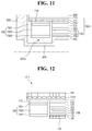
- the panel bottom member 700 - 1 illustrated in FIG. 11 has a difference from the exemplary embodiment of FIG. 6 in that the first vibration sound element 702 is bonded to the light absorbing member 711 by the medium of a separate bonding member 716 .
- the panel bottom member 70 - 1 illustrated in FIG. 12 has a difference from the exemplary embodiment of FIG. 6 in that the first vibration sound element 702 is bonded to the light absorbing member 711 by the medium of a separate bonding member 716 .
- the first interlayer bonding layer 715 and the first vibration sound element 702 may not overlap with each other and may not contact each other.
- the first vibration sound element 702 is not bonded to the light absorbing member 711 by the medium of the first interlayer bonding layer 715 .
- a bonding member 716 may be disposed between the first vibration sound element 702 and the light absorbing member 711 and the first vibration sound element 702 may be bonded to the light absorbing member 711 by the medium of the bonding member 716 .
- the bonding member 716 may be spaced apart from the first interlayer bonding layer 715 .
- the bonding member 716 may include a tape having a bonding property of both sides. In an alternative exemplary embodiment, the bonding member 716 may also include a different material from that of the first interlayer bonding layer 715 .
- FIG. 13 is a cross-sectional view illustrating another modification of FIG. 6
- FIG. 14 is a cross-sectional view illustrating another modification of FIG. 10 .
- the panel bottom member 700 - 2 illustrated in FIG. 13 and the panel bottom member 70 - 2 illustrated in FIG. 14 are arranged to directly contact the lower surface of the light absorbing member 711 without a separate medium.
- the first interlayer bonding layer 715 and the first vibration sound element 702 may not overlap with each other and may not contact each other.
- the first electrode 7021 of the first vibration sound element 702 may directly contact the lower surface of the light absorbing member 711 , and the vibration material layer 7023 is positioned below the first electrode 7021 and the second electrode 7022 may be disposed below the vibration material layer 7023 .
- the structure may be embodied by processes of forming a first electrode 7021 by depositing a conductive layer on the lower surface of the light absorbing member 711 and patterning the conductive layer, forming a vibration material layer 7023 by depositing a vibration material on the first electrode 7021 and the lower surface of the light absorbing member 711 and patterning the vibration material, and forming a second electrode 7022 by depositing a conductive layer on the vibration material layer 7023 and the lower surface of the light absorbing member 711 and patterning the conductive layer, for example.
- the invention is not limited thereto, and the structure may be embodied by various methods.
- FIG. 15 is a cross-sectional view illustrating yet another modification of FIG. 6
- FIG. 16 is a cross-sectional view illustrating yet another modification of FIG. 10 .
- the panel bottom member 700 - 3 illustrated in FIG. 15 and the panel bottom member 70 - 3 illustrated in FIG. 16 further include a digitizer 740 and a third interlayer bonding layer 725 , and other configurations are substantially the same as or similar to each other.
- the digitizer 740 may be disposed below the buffer member 721 and the digitizer 740 may be positioned between the buffer member 721 and the heat dissipation member 730 .
- the digitizer 740 may be positioned below the second interlayer bonding layer 723 to be bonded to the buffer member 721 through the second interlayer bonding layer 723 .
- the third interlayer bonding layer 725 may be positioned between the digitizer 740 and the heat dissipation member 730 and the heat dissipation member 730 may be bonded to the digitizer 740 by the medium of the third interlayer bonding layer 725 .
- the material of the third interlayer bonding layer 725 may include exemplary materials of the top bonding layer 713 described above.
- the digitizer 740 which is one of input devices, receives position information designated by a user on the screen, unlike an input device such as a keyboard or a mouse.
- the digitizer recognizes the motion of, for example, a stylus pen and converts the motion into a digital signal.
- the digitizer may be provided in a form of a film or panel, for example.
- the digitizer 740 may include a wiring pattern 743 and insulating layers 741 and 745 surrounding the wiring pattern 743 at the top and bottom. Particularly, the digitizer 740 may include a first insulating layer 741 , a wiring pattern 743 disposed on the upper surface of the first insulating layer 741 , and a second insulating layer 745 covering the upper surface of the wiring pattern 743 .
- the wiring pattern 743 covers a part of the upper surface of the first insulating layer 741 and exposes another part of the upper surface of the first insulating layer 741 .
- the second insulating layer 745 may be disposed on the upper surface of the exposed first insulating layer 741 as well as the upper surface and the side of each wiring pattern 743 .
- the wiring pattern 743 may include a metallic material such as copper, silver, nickel, and tungsten.
- the wiring pattern 743 may include a single layer or a plurality of laminated layers.
- the wiring pattern 743 may be a double film including a lower copper film and an upper copper film.
- the wiring pattern 743 may include a floating wiring, a floating electrode, and the like as well as wirings or electrodes transferring the signal.
- the first and second insulating layers 741 and 745 may include an organic insulating material, an inorganic insulating material, an organic/inorganic insulating material, or a bonding material such as a bonding material, an adhesive material, or the like.
- the wiring pattern 743 includes a material such as a metal
- the wiring pattern 743 reflects light incident to the top well due to high reflectivity.
- the reflected light is emitted to the display area DA side, the user may recognize the shape of the wiring pattern 743 , and as a result, the image quality of the display device 1 may be adversely affected.
- a step may be provided between a portion where the wiring pattern 743 is positioned and a portion where the wiring pattern 743 is not positioned.
- Such a step shape may be partially reflected even to the upper layer. That is, in the drawing, for clear description, although the upper surface of the second insulating layer 745 is flatly illustrated, but according to another exemplary embodiment, the upper surface of the second insulating layer 745 may have an uneven shape which is not flatted by conformingly reflecting the step shape according to the wiring pattern 743 . Such a surface unevenness may also affect other layers disposed on the top, so that surface unevenness may be partially provided.
- the surface unevenness of the respective layers may have an effect on recognizing a specific pattern from the display screen side by varying the reflectance or the reflection angle (an emitting direction of the reflected light) of the incident light.
- the light absorbing member 711 prevents such reflected light from being emitted to the display area DA. That is, the light absorbing member 711 overlaps with the digitizer 740 to completely cover the digitizer 740 .
- the second insulating layer 745 of the digitizer 740 is in contact with the second interlayer bonding layer 723 and the first insulating layer 741 is in contact with the third interlayer bonding layer 725 , but this is only one example.
- the first insulating layer 741 may contact the second interlayer bonding layer 723 and the second insulating layer 745 may also contact the third interlayer bonding layer 725 .
- the digitizer 740 may not overlap with the vibration sound elements 702 and 703 and may be spaced apart from the vibration sound elements 702 and 703 .
- FIG. 17 is a cross-sectional view illustrating still another modification of FIG. 6
- FIG. 18 is a cross-sectional view illustrating still another modification of FIG. 10 .
- the panel bottom member 700 - 4 illustrated in FIG. 17 and the panel bottom member 70 - 4 illustrated in FIG. 18 further include a digitizer 740 and a third interlayer bonding layer 725 and the first vibration sound element 702 is bonded to the light absorbing member 711 by the medium of a separate bonding member 716 , and other configurations are substantially the same as or similar to each other.
- the description of the digitizer 740 and the third interlayer bonding layer 725 is the same as those described above in the description of FIGS. 15 and 16 , and the description for the bonding member 716 is the same as those described above in the description of FIGS. 11 and 12 . Accordingly, the detailed description will be omitted.
- FIG. 19 is a cross-sectional view illustrating still yet another modification of FIG. 6
- FIG. 20 is a cross-sectional view illustrating still yet another modification of FIG. 10 .
- the panel bottom member 700 - 5 illustrated in FIG. 19 and the panel bottom member 70 - 5 illustrated in FIG. 20 further include a digitizer 740 and a third interlayer bonding layer 725 and the first vibration sound element 702 directly contacts the lower surface of the light absorbing member 711 , and other configurations are substantially the same as or similar to each other.
- the description of the digitizer 740 and the third interlayer bonding layer 725 is the same as those described above in the description of FIGS. 15 and 16 , and the description for the bonding member 716 is the same as those described above in the description of FIGS. 13 and 14 . Accordingly, the detailed description will be omitted.
- FIG. 23 is a schematic diagram for describing another characteristic of the vibration sound element.
- the vibration material layer 7023 When the first vibration sound element 702 is described as an example, the vibration material layer 7023 generates a sound while vibrating by an electric field. However, when the vibration material layer 7023 vibrates by external force F 3 and the like without an electric field, the voltage is generated from the vibration material layer 7023 by an piezoelectric effect. In addition, the generated voltage may be used to transmit sound information to the display device 1 (refer to FIG. 1 ) and position information of an object located outside the display device 1 .
- the first vibration sound element 702 when the first vibration sound element 702 is a microphone, sound waves originating from the outside of the display device 1 may induce vibration in the display panel 500 , and the vibration is transmitted to the vibration material layer 7023 to generate a voltage, for example.
- the generated voltage may be used to transmit sound information to the display device 1 .
- a sensor SED capable of sensing the voltage generated from the vibration material layer 7023 may be additionally provided.
- FIG. 24 is a diagram for describing a proximity sensing operation of the display device according to an exemplary embodiment of the invention.
- the first vibration sound element 702 (refer to FIG. 4 ) positioned in the first element area SA 1 of the display device 1 generates a high-frequency or low-frequency sound wave WA 1 which is not an audible frequency
- the generated sound wave WA 1 is reflected by an object OB outside the display device 1 such as a user.
- a sound wave WA 2 reflected by the object OB may induce vibration in a display panel or the like and the induced vibration is transmitted to the second vibration sound element 703 (refer to FIG. 4 ) positioned in the second element area SA 2 .
- the vibration material layer of the second vibration sound element 703 (refer to FIG. 4 ) vibrates by the vibration transmitted to the second vibration sound element 703 (refer to FIG. 4 ) to generate a voltage.
- whether to be close to the object OB may be sensed by using the generated voltage.
- the sound wave WA 2 reflected by the object OB may be sensed by using the microphone MIC and whether to be close to the object OB may also be sensed by using the sensed sound wave.
- the display device 1 may embody not only a speaker function but also a proximity sensing function by using the vibration sound element without a separate proximity sensor, and further embody various functions such as a microphone function.
- the display panel 500 (refer to FIG. 4 ) for displacement of the proximity sensor, and there is an advantage that the manufacturing process of the display device 1 is simplified.
- each vibration sound element may be varied according to the operation of the display device 1 .
- any one of the first vibration sound element 702 (refer to FIG. 4 ) and the second vibration sound element 703 (refer to FIG. 4 ) has a speaker function for generating sound and the other one may perform a microphone function, for example.
- both the first vibration sound element 702 (refer to FIG. 4 ) and the second vibration sound element 703 (refer to FIG. 4 ) may also perform the speaker function.
- At least one of the first vibration sound element 702 (refer to FIG. 4 ) and the second vibration sound element 703 (refer to FIG. 4 ) may also perform a function of generating the vibration, that is, a haptic function in response to the touch input.
- a display device having a sound function and a panel bottom member for the display device having the sound function.
Abstract
Description
Claims (22)
Applications Claiming Priority (2)
| Application Number | Priority Date | Filing Date | Title |
|---|---|---|---|
| KR1020170085910A KR102367975B1 (en) | 2017-07-06 | 2017-07-06 | Panel bottom member and display device including the same |
| KR10-2017-0085910 | 2017-07-06 |
Publications (2)
| Publication Number | Publication Date |
|---|---|
| US20190014402A1 US20190014402A1 (en) | 2019-01-10 |
| US11064276B2 true US11064276B2 (en) | 2021-07-13 |
Family
ID=64903016
Family Applications (1)
| Application Number | Title | Priority Date | Filing Date |
|---|---|---|---|
| US15/941,572 Active US11064276B2 (en) | 2017-07-06 | 2018-03-30 | Panel bottom member and display device including the same |
Country Status (3)
| Country | Link |
|---|---|
| US (1) | US11064276B2 (en) |
| KR (1) | KR102367975B1 (en) |
| CN (1) | CN109218930B (en) |
Families Citing this family (20)
| Publication number | Priority date | Publication date | Assignee | Title |
|---|---|---|---|---|
| CN109037286B (en) * | 2018-07-26 | 2021-01-26 | 京东方科技集团股份有限公司 | Display device and driving method thereof |
| KR102555303B1 (en) | 2018-10-31 | 2023-07-17 | 삼성디스플레이 주식회사 | Display device and portable device comprising the display device |
| KR102637687B1 (en) | 2018-11-30 | 2024-02-20 | 삼성디스플레이 주식회사 | Display device |
| KR20200094867A (en) * | 2019-01-30 | 2020-08-10 | 삼성디스플레이 주식회사 | Display device |
| CN109887408A (en) * | 2019-02-28 | 2019-06-14 | 西安易朴通讯技术有限公司 | A kind of display panel and terminal |
| KR20200115791A (en) * | 2019-03-26 | 2020-10-08 | 삼성디스플레이 주식회사 | Foldable display device and method for providng the sound of the same |
| KR20200115942A (en) * | 2019-03-29 | 2020-10-08 | 삼성디스플레이 주식회사 | Display device |
| KR20200114910A (en) * | 2019-03-29 | 2020-10-07 | 엘지디스플레이 주식회사 | Display apparatus |
| CN112017529A (en) * | 2019-05-30 | 2020-12-01 | 京东方科技集团股份有限公司 | Display panel buffer structure, display screen module, preparation method of display panel buffer structure and terminal equipment |
| KR20210008205A (en) | 2019-07-10 | 2021-01-21 | 삼성디스플레이 주식회사 | Display device |
| KR20210011306A (en) | 2019-07-22 | 2021-02-01 | 엘지디스플레이 주식회사 | Display apparatus and vehicle comprising the same |
| KR20210011305A (en) * | 2019-07-22 | 2021-02-01 | 엘지디스플레이 주식회사 | Display apparatus and vehicle comprising the same |
| CN112449515A (en) * | 2019-08-27 | 2021-03-05 | Oppo广东移动通信有限公司 | Shell and manufacturing method thereof |
| CN111200779B (en) * | 2019-12-18 | 2021-11-26 | 歌尔微电子有限公司 | Electret microphone and electronic device |
| KR20210085954A (en) * | 2019-12-31 | 2021-07-08 | 엘지디스플레이 주식회사 | Flexible Vibration Film And Display Having The Same |
| TWI768535B (en) * | 2020-03-17 | 2022-06-21 | 群創光電股份有限公司 | Electronic device |
| US20210377670A1 (en) * | 2020-05-29 | 2021-12-02 | Qualcomm Incorporated | Audio speaker and proximity sensor with piezoelectric polymer technology |
| CN111669673B (en) * | 2020-06-08 | 2022-03-22 | 维沃移动通信有限公司 | Loudspeaker module and electronic equipment |
| KR20220050671A (en) * | 2020-10-16 | 2022-04-25 | 엘지디스플레이 주식회사 | Display device |
| US20220131107A1 (en) * | 2020-10-27 | 2022-04-28 | Lg Display Co., Ltd. | Display device |
Citations (16)
| Publication number | Priority date | Publication date | Assignee | Title |
|---|---|---|---|---|
| US20130272557A1 (en) * | 2010-12-31 | 2013-10-17 | Nokia Corporation | Apparatus and method for a sound generating device combined with a display unit |
| CN104122557A (en) | 2013-04-23 | 2014-10-29 | 联想(北京)有限公司 | Method for carrying out ultrasonic detection by using mobile phone and electronic equipment |
| US20140334078A1 (en) * | 2013-05-07 | 2014-11-13 | Samsung Display Co., Ltd. | Display device |
| US20140357321A1 (en) | 2013-05-30 | 2014-12-04 | Nokia Corporation | Panel Speaker Ear Location |
| US20140353623A1 (en) | 2013-05-31 | 2014-12-04 | Samsung Display Co., Ltd. | Organic light emitting display module and display device including the same |
| US8934228B2 (en) | 2011-03-21 | 2015-01-13 | Apple Inc. | Display-based speaker structures for electronic devices |
| US20150016650A1 (en) * | 2013-07-09 | 2015-01-15 | Lg Electronics Inc. | Audio extension module |
| CN104427443A (en) | 2013-08-28 | 2015-03-18 | 胜华科技股份有限公司 | Touch device with loudspeaking function |
| KR20150031641A (en) | 2013-09-16 | 2015-03-25 | 삼성디스플레이 주식회사 | Display device |
| US20150131821A1 (en) * | 2012-05-07 | 2015-05-14 | Kyocera Corporation | Piezoelectric vibration element, and piezoelectric vibration device and portable terminal using piezoelectric vibration element |
| CN104751743A (en) | 2013-12-30 | 2015-07-01 | 三星显示有限公司 | Display device and rear chassis therein |
| US20150255758A1 (en) * | 2014-03-07 | 2015-09-10 | Samsung Display Co., Ltd. | Method of bonding display device |
| US9317063B2 (en) | 2013-07-04 | 2016-04-19 | Samsung Display Co., Ltd. | Display panel and display device having the same |
| US20170115758A1 (en) * | 2015-10-22 | 2017-04-27 | Samsung Display Co., Ltd. | Touch display device and method of manufacturing the same |
| US20170300736A1 (en) * | 2016-04-19 | 2017-10-19 | Samsung Electronics Co., Ltd. | Electronic device supporting fingerprint verification and method for operating the same |
| US20180373913A1 (en) * | 2017-06-26 | 2018-12-27 | Qualcomm Incorporated | Ultrasonic fingerprint sensor for under-display applications |
Family Cites Families (2)
| Publication number | Priority date | Publication date | Assignee | Title |
|---|---|---|---|---|
| US5361163A (en) * | 1991-06-03 | 1994-11-01 | Dai Nippon Printing Co., Ltd. | Reflection type projection screen, production process thereof, and production apparatus thereof |
| KR102350296B1 (en) * | 2015-04-16 | 2022-01-17 | 삼성디스플레이 주식회사 | Organic light emitting display device and manufacturing method thereof |
-
2017
- 2017-07-06 KR KR1020170085910A patent/KR102367975B1/en active IP Right Grant
-
2018
- 2018-03-30 US US15/941,572 patent/US11064276B2/en active Active
- 2018-07-02 CN CN201810708041.4A patent/CN109218930B/en active Active
Patent Citations (21)
| Publication number | Priority date | Publication date | Assignee | Title |
|---|---|---|---|---|
| US20130272557A1 (en) * | 2010-12-31 | 2013-10-17 | Nokia Corporation | Apparatus and method for a sound generating device combined with a display unit |
| US8934228B2 (en) | 2011-03-21 | 2015-01-13 | Apple Inc. | Display-based speaker structures for electronic devices |
| US20150131821A1 (en) * | 2012-05-07 | 2015-05-14 | Kyocera Corporation | Piezoelectric vibration element, and piezoelectric vibration device and portable terminal using piezoelectric vibration element |
| CN104122557A (en) | 2013-04-23 | 2014-10-29 | 联想(北京)有限公司 | Method for carrying out ultrasonic detection by using mobile phone and electronic equipment |
| US20140334078A1 (en) * | 2013-05-07 | 2014-11-13 | Samsung Display Co., Ltd. | Display device |
| KR20140132167A (en) | 2013-05-07 | 2014-11-17 | 삼성디스플레이 주식회사 | Display device |
| US20140357321A1 (en) | 2013-05-30 | 2014-12-04 | Nokia Corporation | Panel Speaker Ear Location |
| US20140353623A1 (en) | 2013-05-31 | 2014-12-04 | Samsung Display Co., Ltd. | Organic light emitting display module and display device including the same |
| CN104218057A (en) | 2013-05-31 | 2014-12-17 | 三星显示有限公司 | Organic light-emitting display apparatus and method of manufacturing the same |
| US9317063B2 (en) | 2013-07-04 | 2016-04-19 | Samsung Display Co., Ltd. | Display panel and display device having the same |
| US20150016650A1 (en) * | 2013-07-09 | 2015-01-15 | Lg Electronics Inc. | Audio extension module |
| CN104427443A (en) | 2013-08-28 | 2015-03-18 | 胜华科技股份有限公司 | Touch device with loudspeaking function |
| KR20150031641A (en) | 2013-09-16 | 2015-03-25 | 삼성디스플레이 주식회사 | Display device |
| CN104751743A (en) | 2013-12-30 | 2015-07-01 | 三星显示有限公司 | Display device and rear chassis therein |
| US20150185963A1 (en) | 2013-12-30 | 2015-07-02 | Samsung Display Co., Ltd. | Display device |
| US10386967B2 (en) | 2013-12-30 | 2019-08-20 | Samsung Display Co., Ltd. | Display device |
| US20190324596A1 (en) | 2013-12-30 | 2019-10-24 | Samsung Display Co., Ltd. | Display device |
| US20150255758A1 (en) * | 2014-03-07 | 2015-09-10 | Samsung Display Co., Ltd. | Method of bonding display device |
| US20170115758A1 (en) * | 2015-10-22 | 2017-04-27 | Samsung Display Co., Ltd. | Touch display device and method of manufacturing the same |
| US20170300736A1 (en) * | 2016-04-19 | 2017-10-19 | Samsung Electronics Co., Ltd. | Electronic device supporting fingerprint verification and method for operating the same |
| US20180373913A1 (en) * | 2017-06-26 | 2018-12-27 | Qualcomm Incorporated | Ultrasonic fingerprint sensor for under-display applications |
Non-Patent Citations (1)
| Title |
|---|
| Chinese Office Action—Chinese Application No. 201810708041.4 dated Oct. 12, 2020, citing references listed within. |
Also Published As
| Publication number | Publication date |
|---|---|
| KR20190006113A (en) | 2019-01-17 |
| US20190014402A1 (en) | 2019-01-10 |
| CN109218930B (en) | 2021-11-19 |
| CN109218930A (en) | 2019-01-15 |
| KR102367975B1 (en) | 2022-02-25 |
Similar Documents
| Publication | Publication Date | Title |
|---|---|---|
| US11064276B2 (en) | Panel bottom member and display device including the same | |
| US11284176B2 (en) | Panel bottom member structure and display device | |
| US10935867B2 (en) | Bottom member and display device including the same | |
| US10911851B2 (en) | Display device and method of driving the same | |
| US11079811B2 (en) | Sound generator including an ultrasound unit, display device including the sound generator, and method of driving display device | |
| US10845912B2 (en) | Display device including force sensor and vibration generator | |
| KR102594035B1 (en) | Display device | |
| US10877585B2 (en) | Display device | |
| US11521415B2 (en) | Display device | |
| US11638076B2 (en) | Display device | |
| US11481032B2 (en) | Display device | |
| US10990181B2 (en) | Display device including a vibrating element |
Legal Events
| Date | Code | Title | Description |
|---|---|---|---|
| AS | Assignment |
Owner name: SAMSUNG DISPLAY CO. LTD., KOREA, REPUBLIC OF Free format text: ASSIGNMENT OF ASSIGNORS INTEREST;ASSIGNORS:AHN, YI JOON;KIM, SUNG CHUL;NOH, JUNG HUN;AND OTHERS;REEL/FRAME:045802/0075 Effective date: 20180320 |
|
| FEPP | Fee payment procedure |
Free format text: ENTITY STATUS SET TO UNDISCOUNTED (ORIGINAL EVENT CODE: BIG.); ENTITY STATUS OF PATENT OWNER: LARGE ENTITY |
|
| STPP | Information on status: patent application and granting procedure in general |
Free format text: NON FINAL ACTION MAILED |
|
| STPP | Information on status: patent application and granting procedure in general |
Free format text: RESPONSE TO NON-FINAL OFFICE ACTION ENTERED AND FORWARDED TO EXAMINER |
|
| STPP | Information on status: patent application and granting procedure in general |
Free format text: FINAL REJECTION MAILED |
|
| STPP | Information on status: patent application and granting procedure in general |
Free format text: RESPONSE AFTER FINAL ACTION FORWARDED TO EXAMINER |
|
| STPP | Information on status: patent application and granting procedure in general |
Free format text: DOCKETED NEW CASE - READY FOR EXAMINATION |
|
| STPP | Information on status: patent application and granting procedure in general |
Free format text: NON FINAL ACTION MAILED |
|
| STPP | Information on status: patent application and granting procedure in general |
Free format text: RESPONSE AFTER FINAL ACTION FORWARDED TO EXAMINER |
|
| STPP | Information on status: patent application and granting procedure in general |
Free format text: NOTICE OF ALLOWANCE MAILED -- APPLICATION RECEIVED IN OFFICE OF PUBLICATIONS |
|
| STPP | Information on status: patent application and granting procedure in general |
Free format text: PUBLICATIONS -- ISSUE FEE PAYMENT RECEIVED |
|
| STPP | Information on status: patent application and granting procedure in general |
Free format text: PUBLICATIONS -- ISSUE FEE PAYMENT VERIFIED |
|
| STCF | Information on status: patent grant |
Free format text: PATENTED CASE |