US11057535B2 - Light guide and image scanning device - Google Patents
Light guide and image scanning device Download PDFInfo
- Publication number
- US11057535B2 US11057535B2 US16/771,911 US201916771911A US11057535B2 US 11057535 B2 US11057535 B2 US 11057535B2 US 201916771911 A US201916771911 A US 201916771911A US 11057535 B2 US11057535 B2 US 11057535B2
- Authority
- US
- United States
- Prior art keywords
- light
- emission surface
- light guide
- incidence angle
- incidents
- Prior art date
- Legal status (The legal status is an assumption and is not a legal conclusion. Google has not performed a legal analysis and makes no representation as to the accuracy of the status listed.)
- Active
Links
- 238000005286 illumination Methods 0.000 claims abstract description 19
- 238000012634 optical imaging Methods 0.000 claims description 12
- 238000013459 approach Methods 0.000 claims description 5
- 230000003287 optical effect Effects 0.000 description 14
- 238000010586 diagram Methods 0.000 description 9
- 239000000853 adhesive Substances 0.000 description 8
- 230000001070 adhesive effect Effects 0.000 description 8
- 239000011347 resin Substances 0.000 description 7
- 229920005989 resin Polymers 0.000 description 7
- 230000006866 deterioration Effects 0.000 description 6
- 238000006243 chemical reaction Methods 0.000 description 5
- 230000000694 effects Effects 0.000 description 4
- 230000017525 heat dissipation Effects 0.000 description 4
- 230000001902 propagating effect Effects 0.000 description 3
- 239000000428 dust Substances 0.000 description 2
- 230000007774 longterm Effects 0.000 description 2
- 239000000463 material Substances 0.000 description 2
- 239000002184 metal Substances 0.000 description 2
- 230000005540 biological transmission Effects 0.000 description 1
- 230000000903 blocking effect Effects 0.000 description 1
- 239000011521 glass Substances 0.000 description 1
- 238000003780 insertion Methods 0.000 description 1
- 230000037431 insertion Effects 0.000 description 1
- 230000001678 irradiating effect Effects 0.000 description 1
- 238000001883 metal evaporation Methods 0.000 description 1
- 238000000034 method Methods 0.000 description 1
- 238000002310 reflectometry Methods 0.000 description 1
- 230000000717 retained effect Effects 0.000 description 1
- 239000004065 semiconductor Substances 0.000 description 1
Images


Classifications
-
- H—ELECTRICITY
- H04—ELECTRIC COMMUNICATION TECHNIQUE
- H04N—PICTORIAL COMMUNICATION, e.g. TELEVISION
- H04N1/00—Scanning, transmission or reproduction of documents or the like, e.g. facsimile transmission; Details thereof
- H04N1/024—Details of scanning heads ; Means for illuminating the original
- H04N1/028—Details of scanning heads ; Means for illuminating the original for picture information pick-up
- H04N1/02815—Means for illuminating the original, not specific to a particular type of pick-up head
- H04N1/0282—Using a single or a few point light sources, e.g. a laser diode
- H04N1/02835—Using a single or a few point light sources, e.g. a laser diode in combination with a light guide, e.g. optical fibre, glass plate
-
- G—PHYSICS
- G02—OPTICS
- G02B—OPTICAL ELEMENTS, SYSTEMS OR APPARATUS
- G02B6/00—Light guides; Structural details of arrangements comprising light guides and other optical elements, e.g. couplings
- G02B6/0001—Light guides; Structural details of arrangements comprising light guides and other optical elements, e.g. couplings specially adapted for lighting devices or systems
- G02B6/0005—Light guides; Structural details of arrangements comprising light guides and other optical elements, e.g. couplings specially adapted for lighting devices or systems the light guides being of the fibre type
- G02B6/0006—Coupling light into the fibre
-
- G—PHYSICS
- G02—OPTICS
- G02B—OPTICAL ELEMENTS, SYSTEMS OR APPARATUS
- G02B6/00—Light guides; Structural details of arrangements comprising light guides and other optical elements, e.g. couplings
- G02B6/0001—Light guides; Structural details of arrangements comprising light guides and other optical elements, e.g. couplings specially adapted for lighting devices or systems
- G02B6/0005—Light guides; Structural details of arrangements comprising light guides and other optical elements, e.g. couplings specially adapted for lighting devices or systems the light guides being of the fibre type
- G02B6/001—Light guides; Structural details of arrangements comprising light guides and other optical elements, e.g. couplings specially adapted for lighting devices or systems the light guides being of the fibre type the light being emitted along at least a portion of the lateral surface of the fibre
-
- G—PHYSICS
- G03—PHOTOGRAPHY; CINEMATOGRAPHY; ANALOGOUS TECHNIQUES USING WAVES OTHER THAN OPTICAL WAVES; ELECTROGRAPHY; HOLOGRAPHY
- G03B—APPARATUS OR ARRANGEMENTS FOR TAKING PHOTOGRAPHS OR FOR PROJECTING OR VIEWING THEM; APPARATUS OR ARRANGEMENTS EMPLOYING ANALOGOUS TECHNIQUES USING WAVES OTHER THAN OPTICAL WAVES; ACCESSORIES THEREFOR
- G03B27/00—Photographic printing apparatus
- G03B27/32—Projection printing apparatus, e.g. enlarger, copying camera
- G03B27/52—Details
- G03B27/54—Lamp housings; Illuminating means
-
- H—ELECTRICITY
- H04—ELECTRIC COMMUNICATION TECHNIQUE
- H04N—PICTORIAL COMMUNICATION, e.g. TELEVISION
- H04N1/00—Scanning, transmission or reproduction of documents or the like, e.g. facsimile transmission; Details thereof
- H04N1/024—Details of scanning heads ; Means for illuminating the original
- H04N1/028—Details of scanning heads ; Means for illuminating the original for picture information pick-up
- H04N1/02815—Means for illuminating the original, not specific to a particular type of pick-up head
- H04N1/0282—Using a single or a few point light sources, e.g. a laser diode
- H04N1/02825—Using a single or a few point light sources, e.g. a laser diode in combination with at least one reflector which is fixed in relation to the light source
-
- H—ELECTRICITY
- H04—ELECTRIC COMMUNICATION TECHNIQUE
- H04N—PICTORIAL COMMUNICATION, e.g. TELEVISION
- H04N1/00—Scanning, transmission or reproduction of documents or the like, e.g. facsimile transmission; Details thereof
- H04N1/04—Scanning arrangements, i.e. arrangements for the displacement of active reading or reproducing elements relative to the original or reproducing medium, or vice versa
Definitions
- the present disclosure relates to a light guide used in an image scanning device such as a facsimile, a copy machine, or a scanner, and to an image scanning device.
- Patent Literature 1 discloses an image scanning device mounted with an illumination device using a light guide that is parabolic in shape.
- Patent Literature 1 Unexamined Japanese Patent Application Publication No 2004-266313
- Patent Literature 1 discloses a light guide provided with, to reflect light from a light source and to propagate the light in the light guide, a parabolic surface on an end of the light guide.
- the light emitted from the end of the light guide end has poor optical characteristics for irradiating a scanning target with light stably across an entire scanning area.
- the light guide is made to be long in the X-axis direction in order to irradiate the scanning target with light stably, and this is problematic in that the size of the image scanning device gets increased.
- an object of the present disclosure is to provide a short light guide and a compact image scanning device having stable optical characteristics.
- the light guide according to the present disclosure is rod-shaped and extends in a longitudinal direction to guide light entering the light guide to an illumination target.
- the light guide includes an incident surface, an emission surface, a reflective surface, and a light scatterer.
- the incident surface is provided at the end portion in the longitudinal direction upon which light emitted by the light source incidents.
- the emission surface is flat-shaped, the emission surface emitting the light that enters the light guide through the incident surface to the illumination target.
- the reflective surface has a parabolic shape to generate collimated light directed toward the emission surface by reflecting light from a focal point of the parabolic shape or light from a predetermined area including the focal point.
- the light scatter has a predetermined scattering area to scatter light that entered the light guide through the incident surface and reflect light that entered the light guide through the incident surface in a direction of the reflective surface.
- the emission surface includes a first emission surface that has a predetermined length from the end portion of the light guide facing the light source along the longitudinal direction, the emission surface being set to an angle at which, among the light scattered by the light scatterer, the collimated light generated by the reflective surface is totally reflected.
- extending the light guide is unnecessary because reflection light with poor optical characteristics can be blocked by such inclusion of the first emission surface that has a predetermined length from an end portion of the light guide facing the light source along the longitudinal direction and totally reflects, among the light scattered by the light scatterer, the light reflected off the reflective surface that became the collimated light, and thus a short light guide and a compact image scanning device that have stable optical characteristics can be attained.
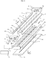
- FIG. 1 is a perspective view of an image scanning device according to Embodiment 1 of the present disclosure
- FIG. 2 is a cross-sectional view of the image scanning device according to Embodiment 1 of the present disclosure
- FIG. 3 is a cross-sectional view of an end portion of the image scanning device according to Embodiment 1 of the present disclosure
- FIG. 4 is an exploded view of the image scanning device according to Embodiment 1 of the present disclosure.
- FIG. 5 is a circuit diagram of the image scanning device according to Embodiment 1 of the present disclosure.
- FIG. 6 is a diagram illustrating illumination paths in the image scanning device according to Embodiment 1 of the present disclosure.
- FIG. 7 is a diagram illustrating paths of light reflected off a parabolic surface of the image scanning device according to Embodiment 1 of the present disclosure.
- FIG. 8 is a diagram illustrating illumination paths in the vicinity of the middle portion of an image scanning device, in the main scanning direction, according to Embodiment 2 of the present disclosure.
- FIG. 9 is a diagram illustrating the illumination paths in an end portion the light source side of the image scanning device according to Embodiment 2 of the present disclosure.
- FIG. 10 is a perspective view of the image scanning device according to Embodiment 2 of the present disclosure.
- FIG. 11 is an exploded view of the image scanning device according to Embodiment 2 of the present disclosure.
- FIG. 12 is a perspective view of an image scanning device according to Embodiment 3 of the present disclosure.
- FIG. 13 is an exploded view of the image scanning device according to Embodiment 3 of the present disclosure.
- X, Y, and Z indicate coordinate axes.
- the X-axis direction is defined as the main scanning direction (longitudinal direction)
- the Y-axis direction is defined as the sub-scanning direction (transverse direction)
- the Z-axis direction is defined as the scanning depth direction.
- the origin of the X-axis is set to the middle of the length of the image scanning device 100 in the main scanning direction.
- the origin of the Y-axis is set to the middle of the length of the image scanning device 100 in the sub-scanning direction.
- the origin of the Z-axis is set to the position to which a document M is fed to be scanned by the image scanning device 100 .
- FIG. 1 is a perspective view of the image scanning device 100 according to Embodiment 1 of the present disclosure.
- FIG. 2 is a cross-sectional view of the image scanning device 100 according to Embodiment 1 of the present disclosure taken along line A-A′ of FIG. 1 .
- FIG. 3 is a cross-sectional view of the image scanning device 100 according to Embodiment 1 taken along B-B′ in FIG. 1 . That is, FIG. 2 is a cross-sectional view of the image scanning device 100 on the YZ plane.
- FIG. 4 is an exploded view of the image scanning device 100 according to Embodiment 1 of the present disclosure. The image scanning device 100 according to Embodiment 1 of the present disclosure is described with reference to FIG. 1 to FIG. 4 .
- the document M is a medium to be scanned such as a banknote, a securities certificate, or another common document.
- the document M is an example of the illumination target.
- Image information of the document M is read by scanning by the image scanning device 100 .
- a light source 1 is a light emitting device such as a light emitting diode (LED) device, an organic electroluminescent (EL) device, and so on.
- LED light emitting diode
- EL organic electroluminescent
- As the light source 1 a light source that emits red light (R), green light (G), blue light (B), white light (H), ultraviolet light (UV), infrared light (IR), and other light in accordance with the image information to be read by scanning is used.
- a light guide 2 is a rod-shaped transparent body that is made of resin or glass for example.
- the light guide 2 extends in the X-axis direction.
- An incident surface 2 d is provided on an end portion of the light guide 2 in the X-axis direction.
- the light source 1 is arranged to face the incident surface 2 d .
- an infrared cut filter 15 is set between the light source 1 and the incident surface 2 d .
- the light guide 2 includes, at one end in the Z-axis direction, a flat surface 2 e that extends in the X-axis direction.
- the flat surface 2 e has a light scatterer 2 a formed in the X-axis direction.
- the light scatterer 2 a has a scattering area with a predetermined length in the Y-axis direction.
- the light guide 2 includes, at the other end in the Z-axis direction, an emission surface 2 b that extends in the X-axis direction and emits light to outside of the light guide 2 .
- the light guide 2 has, on one side surface of side surfaces thereof that connect the flat surface 2 e and the emission surface 2 b together, a reflective surface 2 c that extends in the X-axis direction.
- the reflective surface 2 c is parabolic thereby reflecting light from the light scatterer 2 a toward the emission surface 2 b.
- the light source 1 and the light guide 2 as a pair are also referred to as an illumination device.
- An optical imaging system 3 is, for example, rod lenses arranged in an array.
- the optical imaging system 3 is set between the document M and a board 6 and is held to a frame 5 by a retaining member 10 such as an adhesive or tape.
- the optical imaging system 3 has functionality to condense light emitted from the illumination device and reflected off the document M, and form an image on a sensor IC 4 .
- the sensor IC 4 receives the light condensed by the optical imaging system 3 , performs photoelectric conversion on the received light, and outputs an electrical signal.
- the sensor IC 4 includes a light receiver having a semiconductor chip and the like, a drive circuit, and the like.
- the sensor IC 4 is an example of the light receiving device.
- the frame 5 is set between the board 6 and the optical imaging system 3 is formed of resin or sheet metal.
- the frame 5 has an effect of blocking light entering the sensor IC 4 from the outside of the image scanning device 100 , and also has a dust proofing effect of preventing ingress of dust or the like into the sensor IC 4 .
- the frame 5 is an example of the housing.
- the frame 5 is provided with an opening portion 5 a extending in the X-axis direction and includes flat surface portions 5 b , a pair of inclined portions 5 c , and side wall portions 5 d .
- the flat surface portions 5 b extend in the X-axis direction.
- Both inclined portions 5 c stand upward towards the document M side from the end portion on the opening portion 5 a side of the flat surface portion 5 b in the Y-axis direction.
- the side wall portions 5 d stand upward towards the document M side from the respective end portions that are opposite to the opening portion 5 a of the flat surface portions 5 b in the Y-axis direction.
- Both inclined portions 5 c are inclined such that the gap of the opening portion 5 a in the Y-axis direction narrows as the inclined portions 5 c approach the side of the document M. That is, the inclined portions 5 c have a gap therebetween extending in the X-axis direction.
- Holder mounts 5 e are provided on both ends of the flat surface portion 5 b in the X-axis direction and the holder mounts 5 e each have a bottom surface coplanar with a bottom surface of the corresponding flat surface portion 5 b.
- the light guide 2 is arranged such that the flat surface 2 e faces the flat surface portion 5 b of the frame 5 .
- the light guide 2 is arranged such that the light guide 2 is sandwiched between the inclined portion 5 c and the side wall portion 5 d .
- the reflective surface 2 c of the light guide 2 is located on the side wall portion 5 d side.
- Two such light guides 2 are disposed symmetrically relative to a plan passing through the optical imaging system 3 .
- the rod lenses that constitute the optical imaging system 3 are inserted in the gap of the pair of inclined portions 5 c and are retained within the pair of inclined portions 5 c by the retaining member 10 such as adhesives or tape.
- an external connector 18 and other electronic components, such as an application specific integrated circuit (ASIC) 11 are mounted on the board 6 .
- the ASIC 11 is a signal processing IC.
- components such as a central processing unit (CPU) 12 a , a random access memory (RAM) 12 b , and a signal processing circuit 12 c of the ASIC 11 operate together, thereby enabling the ASIC 11 to process signals such as outputs obtained by photoelectric conversion by the sensor IC 4 of the received light.
- the CPU 12 a , the RAM 12 b , and the signal processing circuit 12 c of the ASIC 11 are collectively referred to as a signal processor 12 .
- the board 6 is fixed to the frame 5 using tape, an adhesive, a screw, or the like.
- the board 6 is fixed to a surface of the flat surface portion 5 b of the frame 5 that is opposite to a surface of the flat surface portion 5 b on which the light guide 2 is disposed.
- the optical axis of the optical imaging system 3 aligns with the light receiver of the sensor IC 4 .
- a holder 7 is provided on one end portion of the light guide 2 in the X-axis direction.
- the end portion of the light guide 2 is inserted into a hole portion 7 a of the holder 7 .
- the holder 7 with the light guide 2 inserted therein is fixed to the holder mount 5 e of the frame 5 using tape, an adhesive, a screw, or the like.
- the holder 7 is formed of white resin, for example.
- the light guide 2 is disposed such that the flat surface 2 e of the light guide 2 on which the light scatterer 2 a is provided faces the flat surface portion 5 b of the frame 5 .
- the holder 8 is provided on the other end portion of the light guide 2 in the X-axis direction. That is, the holder 8 is provided at the end portion of the light guide 2 that is opposite to the end portion thereof on which the holder 7 of the light guide 2 is provided. This end portion of the light guide 2 is inserted into the hole portion 8 a of the holder 8 .
- the holder 8 with the light guide 2 inserted therein is fixed to the holder mount 5 e of the frame 5 using tape, an adhesive, a screw, or the like.
- the holder 8 is formed of white resin, for example.
- the light guide 2 is disposed such that the flat surface 2 e of the light guide 2 on which the light scatterer 2 a is provided faces the flat surface portion 5 b of the frame 5 .
- the light guide 2 is provided, at a position in the vicinity of the middle of the light guide 2 in the X-axis direction, a projection 2 k projecting in the Y-axis direction.
- This projection 2 k is for fixing the light guide 2 to the frame 5 using an adhesive 17 .
- both ends of the light guide 2 are positioned by the holder 7 and the holder 8 , there is no member to restrain light guide 2 in the vicinity of the middle portion of the light guide 2 in the X-axis direction.
- the light guide 2 is fixed at a position as designed by attaching the projection 2 k to the frame 5 while measuring the position of the light guide 2 .
- a single projection 2 k is provided in the current embodiment, multiple projections 2 k may be provided.
- the external connector 18 is used as an interface for input/output signals including photoelectric conversion outputs of the sensor IC 4 and signal processing outputs of such conversion outputs.
- a light source board 9 is a board on which the light source 1 is mounted.
- the light source board 9 is disposed on the surface of the holder 7 that is opposite to the light guide 2 insertion surface of the holder 7 .
- the light source 1 is disposed at a position corresponding to a position of the hole portion 7 a of the holder 7 , and faces the incident surface 2 d of the light guide 2 .
- the light source 1 is provided at one end of the light guide 2 .
- An adhesive heat dissipation sheet 16 is provided on the surface of the light source board 9 that is opposite to the light source 1 mounting surface of the light source board 9 .
- the light source board 9 is fixed to the frame 5 by use of the heat dissipation sheet 16 . In this case, heat generated when the light source 1 is turned on is conducted via the heat dissipation sheet 16 toward the frame 5 that is metallic, and is then dissipated.
- FIG. 5 is a circuit diagram of the image scanning device 100 according to Embodiment 1 of the present disclosure.
- the ASIC 11 works together with the CPU 12 a to send light source turn-on signals to a light source drive circuit 14 .
- the light source drive circuit 14 supplies power to each light source 1 for a predetermined time based on the received light source turn-on signals.
- Each light source 1 emits light during the supplying of power.
- Light emitted by the light source 1 enters the light guide 2 through the incident surface 2 d of the light guide 2 , propagates while repeatedly undergoing transmission or reflection, and reaches the light scatterer 2 a of the light guide 2 .
- Some of light reflected by the light scatterer 2 a is emitted from the emission surface 2 b of the light guide 2 , and is directed toward the document M.
- the light directed toward the document M is reflected off the document M and condensed by the optical imaging system 3 to form an image on the sensor IC 4 .
- FIG. 6 is a diagram illustrating illumination paths in the image scanning device 100 according to Embodiment 1 of the present disclosure.
- FIG. 6 is also a cross-sectional view of the light guide 2 on the YZ plane.
- arrows indicate light rays each indicating a direction of light.
- the light guide 2 includes the light scatterer 2 a on the flat surface 2 e on the frame 5 side of the light guide 2 .
- the flat surface 2 e extends in the X-axis direction, and the light scatterer 2 a is also formed in the X-axis direction.
- the light scatterer 2 a has a scattering area having a predetermined length in the Y-axis direction.
- the light scatterer 2 a is formed by a fine concave and convex patterned surface or embossed surface, or by processing such as silkscreen printing.
- the light scatterer 2 a changes the propagation direction of light by reflecting or refracting light propagating in the light guide 2 in the X-axis direction, thereby enabling irradiation of the document M with light.
- the light scatterer 2 a serves as a second light source.
- the long-term deterioration of the light source 1 does not change brightness or color only in a particular area.
- the flat surface portion 5 b of the frame 5 facing the flat surface 2 e is preferably formed of a material having a high reflectivity such as white resin or metal. This material allows the light having transmitted through the flat surface 2 e including the light scatterer 2 a to be returned into the light guide 2 , thereby enabling efficient illumination.
- the light guide 2 includes the emission surface 2 b that is flat in shape, and the emission surface 2 b is located on the side of the light guide 2 opposite to the flat surface 2 e on which the light scatter 2 a is provided.
- the emission surface 2 b extends in the X-axis direction.
- the light guide 2 includes the reflective surface 2 c connecting the emission surface 2 b and the flat surface 2 e on which the light scatterer 2 a is formed together on one side surface.
- the reflective surface 2 c extends in the X-axis direction and has a parabolic shape as viewed from the YZ plane.
- the light scatterer 2 a is formed, in the YZ plane, at a focal point 2 f of the reflective surface 2 c.
- Light entering the light guide 2 through the incident surface 2 d propagates through the light guide 2 while being guided by the light guide 2 , and then is reflected by the light scatterer 2 a .
- the light reflected by this light scatterer 2 a is then emitted from the emission surface 2 b thereby illuminating the document M.
- some light rays are further reflected off the reflective surface 2 c and are directed to the emission surface 2 b . Since the light scatterer 2 a is formed at the position of the focal point 2 f of the reflective surface 2 c , the light reflected off the reflective surface 2 c is directed toward the emission surface 2 b as collimated light.
- the emission surface 2 b is a flat surface.
- a normal direction of the flat surface of the emission surface 2 b is set to an angle at which the collimated light reflected off the reflective surface 2 c is totally reflected.
- the collimated light directed toward the emission surface 2 b is reflected off the emission surface 2 b and directed onto the light scatterer 2 a again while propagating in the light guide 2 .
- the light re-entering the light scatterer 2 a is scattered and reflected, thereby enabling uniformity in the effect on an illuminance distribution of the light emitting surface of the light source 1 .
- the emission surface 2 b is an example of the first emission surface.
- Optical characteristics of the end portion on the light source 1 side in the X-axis direction tend to deteriorate because a light amount distribution of the light emitting surface of the light source 1 is transferred as collimated light onto the document M when the light entering the light guide 2 from the light source 1 through the incident surface 2 d , directed onto the light scatterer 2 a directly, and reflected off the reflective surface 2 c reaches the document M.
- the light directed onto the light scatterer 2 a directly and reflected off the reflective surface 2 c is referred to as direct reflection light.
- the direct reflection light can be blocked by setting an angle of the normal line of the emission surface 2 b to an angle at which the direct reflection light is to be totally reflected.
- the optical characteristics of the end portion on the light source 1 side in the X-axis direction are stable.
- the angle between the normal line of the emission surface 2 b and the collimated light reflected off the reflective surface 2 c , that is, the incidence angle (I) at which the collimated light reflected off the reflective surface 2 c enters the emission surface 2 b is preferably an angle at which the collimated light reflected off the reflective surface 2 c is totally reflected. This angle is 40° or more in a case where the light guide 2 is transparent resin.
- Light directed from the emission surface 2 b of the light guide 2 onto the document M does not include the direct reflection light from the reflective surface 2 c that would otherwise cause deterioration of optical characteristics of the end portion. This achieves uniform and stable optical characteristics over the light guide 2 in the main scanning direction. Therefore, the light guide 2 , not including an area causing deterioration of the optical characteristics, can be shortened in the X-axis direction (longitudinal direction), and thus an illumination device and an image scanning device that are compact can be attained.
- the reflective surface 2 c may be set to be a mirror surface by performing metal evaporation or the like on the outside of the side surface on which the reflective surface 2 c is formed.
- Embodiment 2 of the present disclosure is described with reference to FIG. 8 to FIG. 11 .
- the emission surface 2 b is set to be the same angle along the X-axis direction, the direct reflection light causing deterioration of the optical characteristics at the end portion only occurs on the end portion on the side of the light source 1 in the X-axis direction. Therefore, in Embodiment 2, the emission surface 2 b is formed, at an angle at which the collimated light from the reflective surface 2 c is totally reflected, only at the end portion on the side of the light source 1 in the X-axis direction, FIG. 10 and FIG. 11 respectively illustrate a perspective view and an exploded view of an image scanning device according to Embodiment 2.
- the light guide 2 includes, on the holder 7 side being the side on which the light source 1 is provided, the emission surface 2 b at an angle at which collimated light from the reflective surface 2 c is totally reflected. Also, on the light guide 2 , an emission surface 2 i , at an angle at which the collimated light from the reflective surface 2 c is emitted, is continuous with the emission surface 2 b and extends toward the holder 8 side in the X-axis direction.
- FIG. 8 illustrates a light ray diagram in the vicinity of the middle portion of the light guide 2 in the X-axis direction in Embodiment 2.
- FIG. 9 illustrates a light ray diagram of an end portion on the light source 1 side of the light guide 2 in the X-axis direction in Embodiment 2.
- the emission surface 2 b is formed at an angle at which the reflection light from the reflective surface 2 c is totally reflected.
- the angle between the normal line of the emission surface 2 b and the collimated light reflected off the reflective surface 2 c is set to 40° or more, thereby totally reflecting the collimated light, and preventing irradiation of the document M with the direct reflection light.
- the emission surface 2 i is set at an angle at which the reflection light from the reflective surface 2 c passes through the emission surface 2 i . In the area away from the light source 1 , the illuminance distribution of the light emitting surface held by the light source 1 becomes uniform as the light propagates in the light guide 2 .
- the emission surface 2 i which is provided in the area other than the end portion on the light source 1 side, is set at an angle at which the collimated light reflected off the reflective surface 2 c enters through, the light that does not include components that cause the characteristics of the end portion to deteriorate is transmitted through the emission surface 2 i thereby illuminating the document M as illustrated in FIG. 8 .
- the light guide 2 is formed of transparent resin, the collimated light reflected off the reflective surface 2 c is transmitted through the emission surface 2 i when the collimated light incidents the emission surface 2 i at an incidence angle that is less than 40°. As illustrated in FIG.
- the emission surface 2 i is formed such that the collimated light reflected off reflective surface 2 c is parallel with the normal line of the emission surface 2 i , meaning that the incidence angle is set to 0°, illumination can be performed in the most efficiently.
- the emission surface 2 i is an example of the second emission surface.
- the direction reflection light can be blocked. In doing so, uniform optical characteristics in all areas in the X-axis direction can be attained, thereby enabling efficient illumination to be performed.
- an emission surface may be provided between the emission surface 2 b and the emission surface 2 i to connect both surfaces together in a manner such that the change in angle from the angle of the emission surface 2 i to the angle of the emission surface 2 b occurs in a stepped manner.
- This emission surface between the emission surface 2 b and the emission surface 2 i is an example of the third emission surface.
- Embodiment 2 although the emission surface 2 b is provided on the end portion of the light source 1 side in the X-axis direction, in Embodiment 3, the emission surface 2 b that totally reflects the collimated light from the reflective surface 2 c and the emission surface 2 i through which the collimated light from the reflective surface 2 c transmits are connected in a continuous manner with varying angles.
- an emission surface 2 j is provided between the emission surface 2 b and the emission surface 2 i .
- This emission surface 2 j connecting the emission surface 2 b and the emission surface 2 i provides continuous angular variation starting from the angle of the emission surface 2 b and ending at the angle of the emission surface 2 i . This can reduce the sudden changes in the emission light amount resulting from the angular difference between the emission surface 2 i and the emission surface 2 b.
- FIG. 12 and FIG. 13 respectively illustrate a perspective view and an exploded view of an image scanning device according to Embodiment 3.
- Providing the emission surface 2 j having continuous angular variation, as illustrated in FIG. 12 and FIG. 13 allows the change in the emission light amount between the emission surface 2 i and the emission surface 2 b to be smoothened. Therefore, by adjusting the density of the fine concave and convex patterns of the light scatterer 2 a , the amount of light emitted from the emission surface 2 i can be adjusted, and thus illumination can be provided at a uniform brightness along the main scanning direction.
- the emission surface 2 j is an example of the third emission surface.
Landscapes
- Physics & Mathematics (AREA)
- Optics & Photonics (AREA)
- Engineering & Computer Science (AREA)
- Multimedia (AREA)
- Signal Processing (AREA)
- General Physics & Mathematics (AREA)
- Facsimile Scanning Arrangements (AREA)
- Facsimile Heads (AREA)
- Planar Illumination Modules (AREA)
- Light Sources And Details Of Projection-Printing Devices (AREA)
Abstract
Description
- 1 Light source
- 2 Light guide
- 2 a Light scatterer
- 2 b Emission surface
- 2 c Reflective surface
- 2 d Incident surface
- 2 e Flat surface
- 2 f Focal point
- 2 g Inclined surface
- 2 i Emission surface
- 2 j Emission surface
- 2 k Projection
- 3 Optical imaging system
- 4 Sensor IC
- 5 Frame
- 5 a Opening portion
- 5 b Flat surface portion
- 5 c Inclined portion
- 5 d Side wall portion
- 5 e Holder mount
- 6 Board
- 7 Holder
- 7 a Hole portion
- 8 Holder
- 8 a Hole portion
- 9 Light source board
- 10 Retaining member
- 11 ASIC
- 12 Signal processor
- 12 a CPU
- 12 b RAM
- 12 c Signal processing circuit
- 13 A/D conversion circuit
- 14 Light source drive circuit
- 15 Infrared cut filter
- 16 Heat dissipation sheet
- 17 Adhesive
- 18 External connector
- 100 Image scanning device
- M Document
Claims (13)
Applications Claiming Priority (4)
| Application Number | Priority Date | Filing Date | Title |
|---|---|---|---|
| JP2018-117551 | 2018-06-21 | ||
| JPJP2018-117551 | 2018-06-21 | ||
| JP2018117551 | 2018-06-21 | ||
| PCT/JP2019/016245 WO2019244459A1 (en) | 2018-06-21 | 2019-04-16 | Illuminating device and image reading device |
Publications (2)
| Publication Number | Publication Date |
|---|---|
| US20200396353A1 US20200396353A1 (en) | 2020-12-17 |
| US11057535B2 true US11057535B2 (en) | 2021-07-06 |
Family
ID=68983131
Family Applications (1)
| Application Number | Title | Priority Date | Filing Date |
|---|---|---|---|
| US16/771,911 Active US11057535B2 (en) | 2018-06-21 | 2019-04-16 | Light guide and image scanning device |
Country Status (5)
| Country | Link |
|---|---|
| US (1) | US11057535B2 (en) |
| JP (1) | JP6661844B1 (en) |
| CN (1) | CN112313931B (en) |
| DE (1) | DE112019003090T5 (en) |
| WO (1) | WO2019244459A1 (en) |
Citations (8)
| Publication number | Priority date | Publication date | Assignee | Title |
|---|---|---|---|---|
| JPH1155464A (en) | 1997-08-06 | 1999-02-26 | Rohm Co Ltd | Light guide member, linear light source device using the light guide member and image reader |
| JPH11215302A (en) | 1998-01-26 | 1999-08-06 | Rohm Co Ltd | Image reader and resin package type light source |
| US6259082B1 (en) | 1997-07-31 | 2001-07-10 | Rohm Co., Ltd. | Image reading apparatus |
| JP2004266313A (en) | 2003-01-16 | 2004-09-24 | Rohm Co Ltd | Image reading apparatus |
| JP2006073383A (en) | 2004-09-02 | 2006-03-16 | Yuka Denshi Co Ltd | Light emitting unit |
| US20160212294A1 (en) * | 2015-01-20 | 2016-07-21 | Konica Minolta, Inc. | Light guide, illuminating device, and image reading apparatus |
| US20160277623A1 (en) * | 2015-03-18 | 2016-09-22 | Kyocera Document Solutions Inc. | Light guide, illuminating device, and image reading device |
| US20200344377A1 (en) * | 2019-04-26 | 2020-10-29 | Mitsubishi Electric Corporation | Image scanning device |
Family Cites Families (2)
| Publication number | Priority date | Publication date | Assignee | Title |
|---|---|---|---|---|
| WO2005001528A1 (en) * | 2003-06-25 | 2005-01-06 | Nippon Sheet Glass Co., Ltd. | Light guide and image reader |
| JP5518953B2 (en) * | 2011-08-09 | 2014-06-11 | キヤノン・コンポーネンツ株式会社 | Image sensor unit and image reading apparatus |
-
2019
- 2019-04-16 DE DE112019003090.6T patent/DE112019003090T5/en active Pending
- 2019-04-16 JP JP2019546413A patent/JP6661844B1/en active Active
- 2019-04-16 WO PCT/JP2019/016245 patent/WO2019244459A1/en active Application Filing
- 2019-04-16 US US16/771,911 patent/US11057535B2/en active Active
- 2019-04-16 CN CN201980040587.XA patent/CN112313931B/en active Active
Patent Citations (9)
| Publication number | Priority date | Publication date | Assignee | Title |
|---|---|---|---|---|
| US6259082B1 (en) | 1997-07-31 | 2001-07-10 | Rohm Co., Ltd. | Image reading apparatus |
| JPH1155464A (en) | 1997-08-06 | 1999-02-26 | Rohm Co Ltd | Light guide member, linear light source device using the light guide member and image reader |
| JPH11215302A (en) | 1998-01-26 | 1999-08-06 | Rohm Co Ltd | Image reader and resin package type light source |
| JP2004266313A (en) | 2003-01-16 | 2004-09-24 | Rohm Co Ltd | Image reading apparatus |
| US20060098247A1 (en) | 2003-01-16 | 2006-05-11 | Rohm Co., Ltd | Image reading device |
| JP2006073383A (en) | 2004-09-02 | 2006-03-16 | Yuka Denshi Co Ltd | Light emitting unit |
| US20160212294A1 (en) * | 2015-01-20 | 2016-07-21 | Konica Minolta, Inc. | Light guide, illuminating device, and image reading apparatus |
| US20160277623A1 (en) * | 2015-03-18 | 2016-09-22 | Kyocera Document Solutions Inc. | Light guide, illuminating device, and image reading device |
| US20200344377A1 (en) * | 2019-04-26 | 2020-10-29 | Mitsubishi Electric Corporation | Image scanning device |
Non-Patent Citations (1)
| Title |
|---|
| International Search Report dated Jun. 18, 2019 in PCT/JP2019/016245 filed Apr. 16, 2019, 1 page. |
Also Published As
| Publication number | Publication date |
|---|---|
| CN112313931A (en) | 2021-02-02 |
| US20200396353A1 (en) | 2020-12-17 |
| DE112019003090T5 (en) | 2021-04-22 |
| CN112313931B (en) | 2022-07-19 |
| JP6661844B1 (en) | 2020-03-11 |
| JPWO2019244459A1 (en) | 2020-06-25 |
| WO2019244459A1 (en) | 2019-12-26 |
Similar Documents
| Publication | Publication Date | Title |
|---|---|---|
| US9841549B2 (en) | Light guide, light source device, and image reading device | |
| US7085023B2 (en) | Image-reading apparatus | |
| US10536603B2 (en) | Light guide and image reading apparatus | |
| US9167121B2 (en) | Lighting unit and image scanner using same | |
| KR20150084904A (en) | Image read-in device | |
| US10911632B2 (en) | Image scanning device | |
| US8576460B2 (en) | Image reading device | |
| US8702280B2 (en) | Light source device | |
| JP2010045755A (en) | Illuminator and image reading apparatus using the same | |
| JP6479286B2 (en) | Illumination device and image reading device | |
| US11057535B2 (en) | Light guide and image scanning device | |
| JP5132648B2 (en) | Illumination device and image reading device | |
| JP6075216B2 (en) | Illumination apparatus and image reading apparatus using the same | |
| CN110785988B (en) | Light guide and image reading apparatus | |
| JP2003348299A (en) | Line illuminator and reader | |
| US11233917B2 (en) | Lighting device and image reading device |
Legal Events
| Date | Code | Title | Description |
|---|---|---|---|
| AS | Assignment |
Owner name: MITSUBISHI ELECTRIC CORPORATION, JAPAN Free format text: ASSIGNMENT OF ASSIGNORS INTEREST;ASSIGNORS:MATSUZAWA, TAKU;SHIRAKI, TORU;OHAMA, DAISUKE;AND OTHERS;REEL/FRAME:052909/0968 Effective date: 20200507 |
|
| FEPP | Fee payment procedure |
Free format text: ENTITY STATUS SET TO UNDISCOUNTED (ORIGINAL EVENT CODE: BIG.); ENTITY STATUS OF PATENT OWNER: LARGE ENTITY |
|
| STPP | Information on status: patent application and granting procedure in general |
Free format text: NON FINAL ACTION MAILED |
|
| STPP | Information on status: patent application and granting procedure in general |
Free format text: RESPONSE TO NON-FINAL OFFICE ACTION ENTERED AND FORWARDED TO EXAMINER |
|
| STPP | Information on status: patent application and granting procedure in general |
Free format text: NOTICE OF ALLOWANCE MAILED -- APPLICATION RECEIVED IN OFFICE OF PUBLICATIONS |
|
| STPP | Information on status: patent application and granting procedure in general |
Free format text: PUBLICATIONS -- ISSUE FEE PAYMENT RECEIVED |
|
| STPP | Information on status: patent application and granting procedure in general |
Free format text: PUBLICATIONS -- ISSUE FEE PAYMENT VERIFIED |
|
| STCF | Information on status: patent grant |
Free format text: PATENTED CASE |
|
| MAFP | Maintenance fee payment |
Free format text: PAYMENT OF MAINTENANCE FEE, 4TH YEAR, LARGE ENTITY (ORIGINAL EVENT CODE: M1551); ENTITY STATUS OF PATENT OWNER: LARGE ENTITY Year of fee payment: 4 |