US11049872B2 - Semiconductor storage device and method of manufacturing the same - Google Patents
Semiconductor storage device and method of manufacturing the same Download PDFInfo
- Publication number
- US11049872B2 US11049872B2 US16/283,589 US201916283589A US11049872B2 US 11049872 B2 US11049872 B2 US 11049872B2 US 201916283589 A US201916283589 A US 201916283589A US 11049872 B2 US11049872 B2 US 11049872B2
- Authority
- US
- United States
- Prior art keywords
- area
- layer
- insulating
- insulating layer
- storage device
- Prior art date
- Legal status (The legal status is an assumption and is not a legal conclusion. Google has not performed a legal analysis and makes no representation as to the accuracy of the status listed.)
- Active
Links
Images


Classifications
-
- H—ELECTRICITY
- H10—SEMICONDUCTOR DEVICES; ELECTRIC SOLID-STATE DEVICES NOT OTHERWISE PROVIDED FOR
- H10B—ELECTRONIC MEMORY DEVICES
- H10B43/00—EEPROM devices comprising charge-trapping gate insulators
- H10B43/10—EEPROM devices comprising charge-trapping gate insulators characterised by the top-view layout
-
- H—ELECTRICITY
- H10—SEMICONDUCTOR DEVICES; ELECTRIC SOLID-STATE DEVICES NOT OTHERWISE PROVIDED FOR
- H10B—ELECTRONIC MEMORY DEVICES
- H10B43/00—EEPROM devices comprising charge-trapping gate insulators
- H10B43/20—EEPROM devices comprising charge-trapping gate insulators characterised by three-dimensional [3D] arrangements, e.g. with cells on different height levels
- H10B43/23—EEPROM devices comprising charge-trapping gate insulators characterised by three-dimensional [3D] arrangements, e.g. with cells on different height levels with source and drain on different levels, e.g. with sloping channels
- H10B43/27—EEPROM devices comprising charge-trapping gate insulators characterised by three-dimensional [3D] arrangements, e.g. with cells on different height levels with source and drain on different levels, e.g. with sloping channels the channels comprising vertical portions, e.g. U-shaped channels
-
- H—ELECTRICITY
- H10—SEMICONDUCTOR DEVICES; ELECTRIC SOLID-STATE DEVICES NOT OTHERWISE PROVIDED FOR
- H10B—ELECTRONIC MEMORY DEVICES
- H10B41/00—Electrically erasable-and-programmable ROM [EEPROM] devices comprising floating gates
- H10B41/40—Electrically erasable-and-programmable ROM [EEPROM] devices comprising floating gates characterised by the peripheral circuit region
- H10B41/42—Simultaneous manufacture of periphery and memory cells
-
- H01L27/11582—
-
- G—PHYSICS
- G11—INFORMATION STORAGE
- G11C—STATIC STORES
- G11C5/00—Details of stores covered by group G11C11/00
- G11C5/06—Arrangements for interconnecting storage elements electrically, e.g. by wiring
- G11C5/063—Voltage and signal distribution in integrated semi-conductor memory access lines, e.g. word-line, bit-line, cross-over resistance, propagation delay
-
- H01L27/1157—
-
- H01L27/11573—
-
- H—ELECTRICITY
- H10—SEMICONDUCTOR DEVICES; ELECTRIC SOLID-STATE DEVICES NOT OTHERWISE PROVIDED FOR
- H10B—ELECTRONIC MEMORY DEVICES
- H10B41/00—Electrically erasable-and-programmable ROM [EEPROM] devices comprising floating gates
- H10B41/20—Electrically erasable-and-programmable ROM [EEPROM] devices comprising floating gates characterised by three-dimensional [3D] arrangements, e.g. with cells on different height levels
-
- H—ELECTRICITY
- H10—SEMICONDUCTOR DEVICES; ELECTRIC SOLID-STATE DEVICES NOT OTHERWISE PROVIDED FOR
- H10B—ELECTRONIC MEMORY DEVICES
- H10B43/00—EEPROM devices comprising charge-trapping gate insulators
- H10B43/20—EEPROM devices comprising charge-trapping gate insulators characterised by three-dimensional [3D] arrangements, e.g. with cells on different height levels
-
- H—ELECTRICITY
- H10—SEMICONDUCTOR DEVICES; ELECTRIC SOLID-STATE DEVICES NOT OTHERWISE PROVIDED FOR
- H10B—ELECTRONIC MEMORY DEVICES
- H10B43/00—EEPROM devices comprising charge-trapping gate insulators
- H10B43/30—EEPROM devices comprising charge-trapping gate insulators characterised by the memory core region
- H10B43/35—EEPROM devices comprising charge-trapping gate insulators characterised by the memory core region with cell select transistors, e.g. NAND
-
- H—ELECTRICITY
- H10—SEMICONDUCTOR DEVICES; ELECTRIC SOLID-STATE DEVICES NOT OTHERWISE PROVIDED FOR
- H10B—ELECTRONIC MEMORY DEVICES
- H10B43/00—EEPROM devices comprising charge-trapping gate insulators
- H10B43/40—EEPROM devices comprising charge-trapping gate insulators characterised by the peripheral circuit region
-
- H—ELECTRICITY
- H10—SEMICONDUCTOR DEVICES; ELECTRIC SOLID-STATE DEVICES NOT OTHERWISE PROVIDED FOR
- H10B—ELECTRONIC MEMORY DEVICES
- H10B43/00—EEPROM devices comprising charge-trapping gate insulators
- H10B43/50—EEPROM devices comprising charge-trapping gate insulators characterised by the boundary region between the core and peripheral circuit regions
-
- G—PHYSICS
- G11—INFORMATION STORAGE
- G11C—STATIC STORES
- G11C16/00—Erasable programmable read-only memories
- G11C16/02—Erasable programmable read-only memories electrically programmable
- G11C16/04—Erasable programmable read-only memories electrically programmable using variable threshold transistors, e.g. FAMOS
- G11C16/0483—Erasable programmable read-only memories electrically programmable using variable threshold transistors, e.g. FAMOS comprising cells having several storage transistors connected in series
Definitions
- Embodiments described herein relate generally to a semiconductor storage device and a method of manufacturing the same.
- a semiconductor storage device in which memory cells are three-dimensionally arranged is known.
- Examples of related art include JP-A-2014-187324.
- FIG. 1 is a block diagram illustrating a circuit configuration of a semiconductor storage device according to a first embodiment.
- FIG. 2 is a circuit diagram of a block in a memory-cell array according to the first embodiment.
- FIG. 3 is a layout diagram illustrating a structure block in the semiconductor storage device according to the first embodiment.
- FIG. 4 is a view illustrating a planar structure of the semiconductor storage device according to the first embodiment.
- FIG. 5 is a cross-sectional view taken along line A-A′ in FIG. 4 .
- FIG. 6 is a cross-sectional view taken along line B-B′ in FIG. 4 .
- FIG. 7 is a cross-sectional view of a memory cell transistor in a cell array area according to the first embodiment.
- FIG. 8 is a cross-sectional view of a structure in the manufacturing process of the semiconductor storage device according to the first embodiment.
- FIG. 9 is a cross-sectional view of a structure in the manufacturing process of the semiconductor storage device according to the first embodiment.
- FIG. 10 is a cross-sectional view of a structure in the manufacturing process of the semiconductor storage device according to the first embodiment.
- FIG. 11 is a cross-sectional view of a structure in the manufacturing process of the semiconductor storage device according to the first embodiment.
- FIG. 12 is a cross-sectional view of a structure in the manufacturing process of the semiconductor storage device according to the first embodiment.
- FIG. 13 is a cross-sectional view of a structure in according to the first embodiment.
- FIG. 14 is a view illustrating a planar structure according to a first modification of the first embodiment.
- FIG. 15 is a view illustrating a planar structure according to a second modification of the first embodiment.
- FIG. 16 is a view illustrating a planar structure of a semiconductor storage device according to a second embodiment.
- FIG. 17 is a cross-sectional view taken along line in the semiconductor storage device according to the second embodiment.
- FIG. 18 is a cross-sectional view of a structure in the manufacturing process of the semiconductor storage device according to the second embodiment.
- FIG. 19 is a cross-sectional view of a structure in the manufacturing process of the semiconductor storage device according to the second embodiment.
- FIG. 20 is a view illustrating a planar structure according to a first modification of the second embodiment.
- FIG. 21 is a view illustrating a planar structure according to a second modification of the second embodiment.
- FIG. 22 is a view illustrating a planar structure according to a third modification of the second embodiment.
- FIG. 23 is a view illustrating a planar structure of a semiconductor storage device accord a third embodiment.
- FIG. 24 a cross-sectional view taken along line A-A′ in the semiconductor storage device according to the third embodiment.
- FIG. 25 is a cross-sectional view of a structure in a manufacturing process of semiconductor storage device according to the third embodiment.
- FIG. 26 is a view illustrating a cross-sectional structure of a semiconductor storage device according to a fourth embodiment.
- FIG. 27 is a cross-sectional view of a structure in a manufacturing process of the semiconductor storage device according to the fourth embodiment.
- FIG. 28 is a cross-sectional view of a structure in a manufacturing process of the semiconductor storage device according to the fourth embodiment.
- FIG. 29 is a cross-sectional view of a structure in a manufacturing process of the semiconductor storage device according to the fourth embodiment.
- FIG. 30 is a cross-sectional view of a structure in a manufacturing process of the semiconductor storage device according to the fourth embodiment.
- FIG. 31 is a cross-sectional view of a structure in a manufacturing process of the semiconductor storage device according to the fourth embodiment.
- FIG. 32 is a cross-sectional view of a structure in a manufacturing process of the semiconductor storage device according to the fourth embodiment.
- FIG. 33A is a view illustrating a planar structure of a semiconductor storage device according to a fifth embodiment.
- FIG. 33B is a view illustrating a cross-sectional structure of the semiconductor storage device according to the fifth embodiment.
- FIG. 34A is a view illustrating a structure in the manufacturing process of the semiconductor storage device according to the fifth embodiment.
- FIG. 34B is a view illustrating a structure in the manufacturing process of the semiconductor storage device according to the fifth embodiment.
- FIG. 35A is a view illustrating a structure in the manufacturing process of the semiconductor storage device according to the fifth embodiment.
- FIG. 35B is a view illustrating a structure in the manufacturing process of the semiconductor storage device according to the fifth embodiment.
- FIG. 36A is a view illustrating a structure in the manufacturing process of the semiconductor storage device according to the fifth embodiment.
- FIG. 36B is a view illustrating a structure in the manufacturing process of the semiconductor storage device according to the fifth embodiment.
- FIG. 37A is a view illustrating a structure in the manufacturing process of the semiconductor storage device according to the fifth embodiment.
- FIG. 37B is a view illustrating a structure in the manufacturing process of the semiconductor storage device according to the fifth embodiment.
- FIG. 38A is a view illustrating a structure in the manufacturing process of the semiconductor storage device according to the fifth embodiment.
- FIG. 38B is a view illustrating a structure in the manufacturing process of the semiconductor storage device according to the fifth embodiment.
- FIG. 39A is a view illustrating a structure in the manufacturing process of the semiconductor storage device according to the fifth embodiment.
- FIG. 39B is a view illustrating a structure in the manufacturing process of the semiconductor storage device according to the fifth embodiment.
- Embodiments provide a semiconductor storage device capable of improving operation reliability, and a method of manufacturing the same.
- a semiconductor storage device includes a logic circuit which is formed on a substrate, a first area which is formed on the logic circuit and has plural first insulating layers and plural conductive layers alternately stacked in a first direction, plural memory pillars which extend the first area in the first direction, a second area which is formed on the logic circuit and has the plural first insulating layers and plural second insulating layers alternately stacked in the first direction, and a contact plug which extends the second area in the first direction and is connected to the logic circuit.
- Each functional block may be implemented by hardware, computer software, or a combination thereof. It is not indispensable that functional blocks are distinguished from each other as in the following examples. For example, some of the functions may be executed by another functional block which is separate from an exemplified functional block. Furthermore, the exemplified functional block may be divided into finer functional sub-blocks.
- a nonvolatile semiconductor storage device will be described with an example of a three-dimensional stacked NAND type flash memory in which memory cell transistors are stacked on the upper side of a semiconductor substrate.
- FIG. 1 is a block diagram illustrating the circuit configuration of the semiconductor storage device according to the first embodiment.
- a NAND type flash memory 10 as a semiconductor storage device includes a memory cell array 11 , a row decoder 12 , a driver 13 , a sense amplifier 14 , an address register 15 , a command register 16 and a sequencer 17 .
- a controller 20 is externally connected to the NAND type flash memory 10 via a NAND bus. The controller 20 accesses the NAND type flash memory 10 and controls the NAND type flash memory 10 .
- the memory cell array 11 includes plural blocks BLK 0 , BLK 1 , BLK 2 , . . . , BLKn (n is an integer of 0 or more) each including plural nonvolatile memory cells associated with rows and columns.
- a block BLK indicates each of the blocks BLK 0 to BLKn.
- the memory cell array 11 stores data supplied from the controller 20 . Details of the memory cell array 11 and the block BLK will be described later.
- the row decoder 12 selects one of the blocks BLK and further selects a word line in the selected block BLK. Details of the row decoder 12 will be described later.
- the driver 13 supplies a voltage to the selected block BLK via the row decoder 12 .
- the sense amplifier 14 senses data DAT read from the memory cell array 11 and performs a necessary calculation. Then, the sense amplifier outputs the read data DAT to the controller 20 . At the time of data write, the sense amplifier 14 transfers write data DAT received from the controller 20 to the memory cell array 11 .
- the address, register 15 holds an address ADD received from the controller 20 .
- the address ADD includes a block address that designates a block BLK to be operated and a page address that designates a word line to be operated in the designated block.
- the command register 16 holds a command CMD received from the controller 20 .
- the command CMD includes, for example, a write command that instructs the sequencer 17 to perform a write operation and a read command that instructs the sequencer 17 to perform a read operation.
- the sequencer 17 controls the operation of the NAND type flash memory 10 based on the command CMD held in the command register 16 . Specifically, based on the write command held in the command register 16 , the sequencer 17 controls the row decoder 12 , the driver 13 and the sense amplifier 14 to write data in plural memory cell transistors designated by the address ADD. In addition, based on the read command held in the command register 16 , the sequencer 17 controls the row decoder 12 , the driver 13 and the sense amplifier 14 to read data from plural memory cell transistors designated by the address ADD.
- the controller 20 is connected to the NAND type flash memory 10 via the NAND bus.
- the NAND bus transmits and receives signals according to a NAND interface.
- the NAND bus includes a bus that communicates, for example, a chip enable signal CEn, a command latch enable signal CLE, an address latch enable signal ALE, a write enable signal WEn, a read enable signal REn, an input/output signal I/O and a ready/busy signal R/Bn.
- the input/output signal I/O is transmitted with an 8-bit bus width.
- the input/output signal I/O communicates the command CMD, the address ADD, the data DAT and the like.
- the memory cell array 11 includes the blocks BLK 0 to BLKn.
- the blocks BLK 0 to BLKn have the same configuration.
- the circuit configuration of one block BLK will be described below.
- FIG. 2 is a circuit diagram of a block BLK in the memory cell array 11 .
- the block BLK includes, for example, four stringy units SU 0 to SU 3 .
- a “string unit SU” indicates each of the string units SU 0 to SU 3 .
- the string unit SU includes plural NAND strings NS.
- Each of the NAND strings NS includes, for example, eight memory cell transistors MT 0 to MT 7 and select transistors S 1 and S 2 .
- a “memory cell transistor MT” indicates each of the memory cell transistors MT 0 to MT 7 .
- the memory cell transistor (hereinafter, also referred to as a memory cell) MT includes a control gate and a charge storage layer and holds data in a nonvolatile manner.
- the memory cell transistor MT is connected in series between the source of the select transistor S 1 and the drain of the select transistor S 2 .
- the gates of the select transistors S 1 in the string units SU 0 to SU 3 are connected to select gate lines SGD 0 to SGD 3 , respectively.
- the gates of the select transistors S 2 in the string units SU 0 to SU 3 are connected to, for example, one select gate line SGS.
- the gates of the select transistors S 2 may be connected to different select gate lines SGS 0 to SGS 3 for each string unit.
- the control gates of the memory cell transistors MT 0 to MT 7 in the string units SU 0 to SU 3 in the block BLK are connected to word lines WL 0 to WL 7 , respectively.
- each bit line BL is commonly connected to the drains of the select transistors S 1 of the NAND string NS in the same column. That is, each bit line BL connect the NAND strings NS in common between the ultra string units SU 0 to SU 3 in the same column.
- the sources of the plural select transistors 52 are commonly connected to a source line SL. That is, each string unit SU includes plural NAND strings NS connected to different bit lines BL and connected to the same select gate line SGD.
- the block BLK includes plural string units SU that share the word line WL.
- the plural memory cell transistors MT connected to the common word line WL in the string unit SU are referred to as a cell unit CU.
- the storage capacity of the cell unit CU is varied depending on the number of bits of data stored in the memory cell transistor MT. For example, the cell unit CU stores 1-page data when each memory cell transistor MT stores 1-bit data, 2-page data when each memory cell transistor MT stores 2-bit data, and 3-page data when each memory cell transistor MT stores 3-bit data.
- the configuration of the memory cell array 11 is not limited to the above configuration.
- the number of string units SU in each block BLK may be set to any number.
- the number of memory cell transistors MT and select gate transistors S 1 and S 2 in each NAND string NS may also be set to any number.
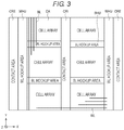
- FIG. 3 is a layout diagram illustrating a structure block in the semiconductor storage device according to the first embodiment.
- two directions which are orthogonal (or intersecting) with each other and parallel to a semiconductor substrate surface are taken as an X direction (A-A′ line direction) and a Y direction (B-B′ line direction), respectively, and a direction which is orthogonal (or intersecting) with the X direction and the Y direction (XY plane) is taken as a Z direction.
- the semiconductor storage device includes a cell array area CA, a bit line hookup area BHU, a word line hookup area WHU, a contact area CRI and a contact area CRE.
- Plural cell array areas CA and plural bit line hookup areas BHU are arranged in a matrix in the X direction and the Y direction.
- the bit line hookup areas BHU are interposed between the cell array areas CA in the Y direction.
- the word line hookup areas WHU are disposed at the ends of the cell array areas CA in the X direction.
- the contact areas CRE are disposed on the opposite side of the word line hookup areas WHU in the X direction to the side where the cell array areas CA are disposed. Further, the contact areas CRI are interposed between the cell array areas CA and between the bit line hookup areas BHU in the X direction.
- Plural bit lines BL extending in the Y direction are arranged in the X direction on the bit line hookup areas BHU and the cell array areas CA. Further, plural word lines WL which extend in the X direction are arranged in the Y direction on the word line hookup areas WHU.
- FIG. 4 is a plan view schematically illustrating the planar structure of the semiconductor storage device according to the first embodiment.
- a bit line hookup area BHU is formed in the Y direction between cell array areas CA.
- a slit (or isolation area) ST 1 is formed between the cell array area CA and the bit line hookup area BHU.
- the slit ST 1 has a plate shape extending in the X direction and the Z direction. The slit ST 1 separates the cell array area CA and the bit line hookup area BHU.
- Plural memory pillars MP and a slit SLT are formed in each cell array area CA.
- the plural memory pillars MP are arranged in a zigzag pattern.
- the slit SLT has a plate shape that extends in the X direction and the Z direction.
- the slit SLT demarcates the plural memory pillars MP in the cell array area CA in the X direction.
- Plural contact plugs CC are formed in the word line hookup area WHU set at an end portion of the cell array area CA in the Y direction. Wiring layers electrically connected to the contact plugs CC are formed on the contact plugs CC. These wiring layers function as word lines WL.
- Plural contact plugs CP 1 are arranged in a zigzag pattern in the bit line hookup area BHU.
- the bit lines BL on the bit line hookup area BHU and the cell array area CA are electrically connected to the memory pillars MP and the contact plugs CP 1 , respectively.
- Plural contact plugs CP 2 are arranged in a zigzag pattern in the contact area CRE.
- the contact plugs CP 2 are electrically connected to wiring layers formed thereon (not illustrated). Further, plural contact plugs (not illustrated) are arranged in a zigzag pattern in the contact area CRI.
- FIG. 5 is a cross-sectional view taken along line A-A′ in FIG. 4 .
- FIG. 6 is a cross-sectional view taken along line B-B′ in FIG. 4 .
- the number of memory pillars MP and contact plugs CP 1 and CP 2 is any number, and the number of memory pillars MP and contact plugs CP 1 and CP 2 in FIG. 4 and the cross-sectional view thereof may not match. This also applies to the following embodiments.
- a peripheral circuit layer PE is formed on a semiconductor substrate (e.g., a silicon single crystal substrate) 30 .
- the peripheral circuit layer PE is provided with peripheral circuits (or logic circuits), for example, the row decoder 12 the driver 13 , the sense amplifier 14 , the address register 15 , the command register 16 , the sequencer 17 and the like as described above.
- element isolation areas 30 A are formed on the semiconductor substrate 30 , and a CMOS circuit including an n-channel MOS field effect transistor hereinafter, referred to as an nMOS transistor) NT and a p-channel MOS field effect transistor (hereinafter, referred to as a pMOS transistor) PT is formed between the element isolation areas 30 A.
- a source area and a drain area are formed between the element isolation areas 30 A, and a gate electrode GE is formed on the semiconductor substrate 30 between the source area and the drain area via a gate insulating film.
- Vias C 1 are formed on the source area and the drain area, respectively.
- a wiring layer D 0 is formed on each via C 1
- a wiring layer (or electrode pad) D 1 is formed on the wiring layer D 0 via a via C 2 .
- a contact plug CP 1 to be described later is formed on the wiring layer D 1 .
- an insulating layer 31 is formed around the nMOS transistor NT, the pMOS transistor PT, the wiring layers D 0 and D 1 and the vias C 1 and C 2 .
- the wiring layers D 0 and D 1 and the vias C 1 and C 2 contain, for example, tungsten (W).
- the insulating layer 31 includes, for example, a silicon oxide layer.
- a conductive layer 32 is formed on the insulating layer 31 .
- the conductive layer 32 includes conductive layers 32 A, 32 B and 32 C arranged from the insulating layer 31 side.
- the conductive layer 32 functions as a source line SL.
- the conductive layers 32 A, 32 B and 32 C contain, for example, polycrystalline silicon or tungsten (W).
- a stacked body including plural insulating layers 33 and plural conductive layers 34 , 35 _ 0 , 35 _ 1 , 35 _ 2 , 35 __ 3 , 35 _ 4 , 35 _ 5 , 35 _ 6 , 35 _ 7 and 36 alternately stacked in the Z direction is formed on the conductive layer 32 .
- the conductive layers 34 , 35 __ 0 to 35 _ 7 and 36 have a plate shape parallel to the XY plane (or the semiconductor substrate 30 plane) and extend in the X direction.
- Each of the conductive layers 34 , 35 _ 0 to 35 _ 7 and 36 extending in the X direction is electrically connected to a wiring layer (not illustrated) extending in the X direction via a contact plug in the word line hookup area WHU.
- the conductive layer 34 functions as a select gate line SGS.
- the conductive layers 35 _ 0 to 35 _ 7 function as word lines WL 0 to WL 7 .
- the conductive layer 36 functions as a select gate line SGD.
- the insulating layer 33 includes, for example, a silicon oxide layer.
- the conductive layers 34 , 35 _ 0 to 35 _ 7 and 36 contain, for example, tungsten (W) or polycrystalline silicon.
- Plural columnar memory pillars MP are formed in the stacked body including the plural insulating layers 33 and the plural conductive layers 34 , 35 _ 0 to 35 _ 7 and 36 .
- Lace memory pillar are MP extends in the Z direction.
- Each memory pillar MP is disposed to penetrate the insulating layer 33 and the conductive layers 34 , 35 _ 0 to 35 _ 7 and 36 in the stacking direction, and reaches the conductive layer 32 from the upper surface of the uppermost insulating layer 33 . That is, the memory pillar MP passes through the select gate line SGD, the plural word lines WL 0 to WL 7 , the select gate line SGS and the plural insulating layers 33 from the upper surface of the insulating layer 33 to be connected to the source line SL. Details of the memory pillar MP will be described later.
- plural slits SLT are formed in the stacked body including the plural insulating layers 33 and the plural conductive layers 34 , 35 _ 0 to 35 _ 7 and 36 .
- the slits SIT separate the stacked body including the plural insulating layers 33 and the plural conductive layers 34 , 35 _ 0 to 35 _ 7 and 36 .
- the slits SLT has a plate shape extending in the X direction and the Z direction.
- the slits SLT include an insulating material, for example, an insulating layer in which silicon oxide layer is buried.
- An insulating layer 37 is formed on the insulating layer 33 .
- a via V 1 extending in the Z direction is formed in the insulating layer 37 on the memory pillar MP.
- An insulating layer 38 is formed on the via V 1 and the insulating layer 37 .
- a via V 2 extending in the Z direction is formed in the insulating layer 38 on the via V 1 .
- a conductive layer (or a wiring, an upper layer wiring) 39 is formed on the via V 2 and the insulating layer 38 .
- the conductive layer 39 is electrically connected to the memory pillar MP via the vias V 2 and V 1 and is further electrically connected to the contact plug CP 1 via the vias V 2 and V 1 in the bit line hookup area BHU.
- the conductive layer 39 functions as a bit line BL.
- the insulating layer 37 includes, for example, a silicon oxide layer.
- the conductive layer 39 and the vias V 1 and V 2 contain, for example, tungsten (W).
- each slit ST 1 has a plate shape extending in the X direction and the Z direction.
- the slit ST 1 separates the stacked body on the conductive layer 32 in the cell array area CA and the stacked body on the conductive layer 32 in the bit line hookup area BHU.
- the upper surface of the slit ST 1 is lower than the upper surface of the slit SLT. That is, the height of the slit ST 1 from the semiconductor substrate surface is lower than the height of the slit SLT from the semiconductor substrate surface.
- the slit ST 1 includes an insulating material, for example, an insulating layer in which at least one of a silicon oxide layer and an aluminum oxide layer is buried.
- the insulating layer 33 is formed on the conductive layer 32 and the conductive layer 34 is formed on the insulating layer 33 .
- a stacked body including plural insulating layers 33 and plural insulating layers 50 alternately stacked in the Z direction is formed on the conductive layer 34 .
- An insulating layer 37 is formed on the uppermost insulating layer 33 .
- Plural columnar contact plugs CP 1 are formed in the insulating layer 37 , the plural insulating layers 33 , the plural insulating layers 50 , the conductive layers 34 and 32 and the insulating layer 31 .
- Each contact plug CP 1 extends in the Z direction.
- Each contact plug CP 1 is disposed to penetrate the plural insulating layers 33 , the plural insulating layers 50 , the conductive layers 34 and 32 and the insulating layer 31 in the stacking direction, and reaches the wiring layer D 1 from the upper surface of the uppermost insulating layer 33 .
- the contact plug CP 1 passes from the upper surface of the insulating layer 33 through the plural insulating layers 33 , the plural insulating layers 50 , the select gate line SGS, the source line SL and the insulating layer 31 , and is connected to the wiring layer D 1 of the peripheral circuit layer PE.
- the contact plug CP 1 has, for example, a conductive layer 52 formed therein and an insulating layer 53 formed on the outer peripheral surface of the conductive layer 52 .
- An insulating layer 51 is formed between the insulating layer 53 of the contact plug CP 1 and the conductive layers 32 and 34 .
- the insulating layer 51 enhances the insulating property between the contact plug CP 1 and the conductive layers 32 and 34 .
- the conductive layer 52 contains, for example, tungsten.
- the insulating layers 51 and 53 include, for example, a silicon oxide layer.
- FIG. 6 is a cross-sectional view of the contact area CRE, the word line hookup area WHU and the bit line hookup area BHU.
- each contact plug CP 1 is formed so as to extend the plural insulating layers 33 , the plural insulating layers 50 , the conductive layers 34 and 32 and the insulating layer 31 in the stacking direction, and reaches the wiring layer D 1 from the upper surface of the uppermost insulating layer 33 .
- each contact plug CP 2 is formed so as to extend the insulating layer 37 , the insulating layer 33 , the conductive layer 32 and the insulating layer 31 in the stacking direction, and reaches the wiring layer D 1 from the upper surface of the uppermost insulating layer 33 .
- An insulating layer 51 is formed between the insulating layer 53 of the contact plug CP 2 and the conductive layer 32 . The insulating layer 51 enhances the insulating property between the contact plug CP 2 and the conductive layer 32 .
- FIG. 7 is a cross-sectional view of the memory cell transistor in the cell array area CA according to the first embodiment. An interlayer insulating film between conductive layers is not illustrated in FIG. 7 .
- the cell array area CA includes conductive layers 32 , 34 , 35 _ 0 to 35 _ 1 and 36 and a memory pillar MP.
- the conductive layer 32 is formed in a plate shape along the XY plane and functions as a source line SL as described above.
- the conductive layers 34 , 35 _ 0 to 35 _ 7 and 36 are formed on the conductive layer 32 in order from the lower layer. Among these conductive layers, conductive layers adjacent in the Z direction are stacked via an interlayer insulating film. The conductive layers 34 , 35 _ 0 to 35 _ 7 and 36 are each formed in a plate shape along the XY plane. As described above, the conductive layer 34 functions as a select gate line SGS. The conductive layers 35 _ 0 to 35 _ 7 function as word lines WL 0 to WL 7 in order from the lower layer, respectively. The conductive layer 36 functions as a select gate line SGD.
- the plural memory pillars MP are arranged in, for example, a zigzag manner in the XY direction.
- Each memory pillar MP functions as one NAND string NS.
- Each memory pillar MP is formed so as to pass through the conductive layers 34 , 35 _ 0 to 35 _ 7 and 36 and reach the upper surface of the conductive layer 32 from the upper surface of the conductive layer 36 .
- the memory pillar MP includes, for example, a cell insulating film 40 , a semiconductor layer 41 and a core insulating film 42 formed in order from the conductive layer side.
- the cell insulating film 40 includes a block insulating film 40 A, a charge storage film (also referred to as a charge storage layer) 40 B and a tunnel insulating film 40 C.
- the block insulating film 40 A is formed on the inner wall of a memory hole that forms the memory pillar MP.
- the charge storage film 40 B is formed on the inner wall of the block insulating film 40 A.
- the tunnel insulating film 40 C is formed on the inner wall of the charge storage film 40 B.
- the semiconductor layer 41 is formed on the inner wall of the tunnel insulating film 40 C.
- the core insulating layer (e.g., a silicon oxide layer) 42 is formed in the semiconductor layer 41 .
- a portion where the memory pillar MP and the conductive layer 34 intersect with each other functions as the select gate transistor S 2 .
- Portions where the memory pillar MP and the conductive layers 35 _ 0 to 35 _ 7 intersect with each other function as the memory cell transistors MT 0 to MT 7 , respectively.
- Each of the memory cell transistors MT 0 to MT 7 is a memory cell in which data may be stored. Data is written in each memory cell transistor MT 0 to MT 7 by a write operation.
- a portion where the memory pillar MP and the conductive layer 36 intersect with each other functions as the select gate transistor S 1 .
- the semiconductor layer 41 functions as a channel layer of the memory cell transistor MT and the select gate transistors S 1 and S 2 .
- a current path of the NAND string NS is formed in the semiconductor layer 41 .
- the charge storage film 40 B has a function of accumulating charges injected from the semiconductor layer 41 in the memory cell transistor MT.
- the charge storage film 40 B includes, for example, a silicon nitride film.
- the tunnel insulating film 40 C functions as a potential barrier when charges are injected from the semiconductor layer 41 into the charge storage film 40 B or when charges accumulated in the charge storage film 40 B diffuse into the semiconductor layer 41 .
- the tunnel insulating film 40 C includes, for example, a silicon oxide film.
- the block insulating film 40 A prevents the charges accumulated in the charge storage film 40 B from diffusing into the conductive layers (word lines WL) 35 _ 0 to 35 _ 7 .
- the block insulating film 40 A includes, for example, a silicon oxide film and a silicon nitride film.
- a via V 1 is formed on the memory pillar MP, and a wiring layer (not illustrated) as a bitline BL is formed on the memory pillar MP.
- the configuration of the memory cell array 11 including the cell array area CA is not limited to the above configuration.
- the number of word lines WL and select gate lines SGD and SGS is changed according to the number of memory cell transistors MT and select gate transistors S 1 and S 2 , respectively.
- the select gate line SGS may be composed of plural conductive layers and the select gate line SGD may be composed of plural conductive layers.
- FIGS. 8 to 13 are cross-sectional views of the structure of each manufacturing process of the semiconductor storage device according to the first embodiment, which are taken along line A-A′ (Y direction) in FIG. 4 .
- the peripheral circuit layer PE, the conductive layers 32 A, 32 D, 32 C and 34 are formed on the semiconductor substrate 30 and the plural insulating layers 33 and the plural insulating layers 50 are stacked to form the memory pillar MP.
- a CMOS circuit including, for example, an nMOS transistor and a pMOS transistor, is formed on the semiconductor substrate 30 , and the via C 1 , the wiring layer D 0 , the via C 2 , the wiring layer D 1 and the like connected to the CMOS circuit are formed.
- the insulating layer 31 is formed on the wiring layer D 1 .
- the peripheral circuit layer PE including the row decoder 12 , the driver 13 , the sense amplifier 14 , the address register 15 , the command register 16 , the sequencer 17 and the like is formed on the semiconductor substrate 30 .
- the conductive layer 32 A, a sacrificial layer (not illustrated), the conductive layer 32 D, a sacrificial layer (not illustrated) and the conductive layer 32 C are formed in order on the insulating layer 31 by, for example, a CVD (Chemical Vapor Deposition) method (or an ALD (Atomic Layer Deposition) method). Further, the insulating layer 33 and the insulating layer 34 are formed in order on the conductive layer 32 C by, for example, a CVD (or ALD) method.
- the conductive layer 32 D includes, for example, a polycrystalline Silicon layer.
- the sacrificial layer includes, for example, a silicon oxide layer. Further in the bit line hookup area BHU, the insulating layer 51 extending through the conductive layers 32 A, 32 D, 32 C and 34 in the Z direction is formed in an area where the contact plug CP 1 is to be formed.
- the plural insulating layers 33 and the plural insulating layers 50 are alternately stacked on the conductive layer 34 by, for example, a CVD (or ALD) method.
- a CVD or ALD
- the stacked body including the insulating layer 33 , the conductive layer 34 , the plural insulating layers 33 and the plural insulating layers 50 alternately stacked is formed.
- the memory pillar MP extending in the Z direction is formed in the stacked body and the conductive layers 32 A, 32 D and 32 C.
- the slit ST 1 is formed between the cell array area CA and the bit line hookup area BHU.
- the insulating layer 37 is formed on the memory pillar MP and the insulating layer 33 by, for example, a CVD (or ALD) method.
- a groove 54 for the slit ST 1 extending in the X direction and the Z direction formed in the insulating layer 37 , the plural insulating layers 33 and the plural insulating layers 50 between the cell array area CA and the bit line hookup area BHU is formed by, for example, a RIE (Reactive Ion Etching) method.
- RIE Reactive Ion Etching
- an insulating material for example, at least one of a silicon oxide layer or an aluminum oxide layer, is buried in the groove 54 by, for example, a CVD (or ALD) method.
- a CVD or ALD
- the slit ST 1 is formed between the cell array area CA and the bit line hookup area BHU.
- the insulating layers (e.g., silicon nitride layers) 50 are replaced with the conductive layers (e.g. tungsten layers) 35 _ 0 to 35 _ 7 and 36 , and the slit SLT that separates the conductive layers 35 _ 0 to 35 _ 7 and 36 is formed. Further, the conductive layer (source line SL) 32 is connected to the memory pillar MP.
- a groove 55 for the slit SLT is formed in the stacked body including the insulating layer 37 , the plural insulating layers 33 , the plural insulating layers 50 , the conductive layer 34 , the insulating layer 33 and the conductive layer 32 by, for example, a RIE method.
- the groove 55 reaches the conductive layer 32 from the surface of the insulating layer 37 .
- the conductive layer (polycrystalline silicon layer) 32 D (see FIG. 10 ) and the sacrificial layers disposed above and below the conductive layer 32 D are removed through the groove 55 by wet etching.
- a gap is formed between the conductive layer 32 A and the conductive layer 32 C.
- a conductive layer 323 is formed by a CVD (or ALD) method so as to fill the gap between the conductive layer 32 A and the conductive layer 32 C.
- the conductive layer 32 B is connected to the memory pillar MP.
- the insulating layer (silicon nitride layer) 50 is removed through the groove 55 by, for example, wet etching using a phosphoric acid solution.
- the insulating layer (silicon oxide layer) 33 is not removed but remains.
- a gap is formed between the insulating layers 33 .
- the gap between the insulating layers 33 is filled with a conductive material such as tungsten by, for example, a CVD (or ALD) method to form the conductive layers 35 _ 0 to 35 _ 7 and 36 .
- an insulating material for example, a silicon oxide layer, is buried in the groove 55 by, for example, a CVD (or ALD) method.
- the slit SLT is formed.
- the bit line hookup area BHU in wet etching using a phosphoric acid solution, the phosphoric acid solution is blocked by the slit ST 1 and does not reach the insulating layers 50 in the bit line hookup area BHU. Therefore, the insulating layers 50 in the bit line hookup area BHU are not removed but remain intact. That is, in the process of replacing the insulating layers with the conductive layers 35 _ 0 to 35 _ 7 and 36 , the insulating layers 50 in the bit line hookup area BHU are not replaced with the conductive layers, and the bit line hookup area BHU maintains the stacked body including the plural insulating layers 33 and the plural insulating layers 50 as they are.
- the contact plug CP 1 is formed in the bit line hookup area BHU.
- an insulating layer 37 is further formed on the slit SLT and the insulating layer 37 by, for example, the CVD (or ALD) method.
- a hole for the contact plug CP 1 is formed in the stacked body including the insulating layer 37 of the bit line hookup area BHU, the plural insulating layers 33 , the plural insulating layers 50 and the insulating layer 51 by, for example, a RIE method.
- the insulating layer 53 is formed on the inner wall of the hole for the contact plug CP 1 by, for example, a CVD (or ALD) method, and the conductive layer 52 is buried in the insulating layer 53 .
- the contact plug CP 1 is formed in the bit line hookup area BHU.
- the vias V 1 and V 2 and the conductive layer 39 connected to the memory pillar MP and the contact plug CP 1 are formed.
- an insulating layer 37 is formed on the contact plug CP 1 and the insulating layer 37 by, for example, a CVD (or ALD) method.
- the via V 1 is formed in the insulating layer 37 on the memory pillar MP and the contact plug CP 1 .
- the insulating layer 38 is formed on the via V 1 and the insulating layer 37 .
- the via V 2 is formed in the insulating layer 38 on the via V 1 .
- the conductive layer 39 is formed on the via V 2 and the insulating layer 38 .
- FIG. 14 illustrates a planar structure of a semiconductor storage device according to the first modification of the first embodiment, and represents, cell array areas CA, word line hookup areas WHU and a bit line hookup area BHU.
- the bit line hookup area BHU is interposed between the cell array areas CA in the Y direction.
- Plural contact plugs CP 1 and a slit (or isolation area) ST 2 are formed in the bit line hookup area BHU.
- the slit ST 2 is disposed around the plural contact plugs CP 1 so as to surround the plural contact plugs CP 1 .
- the slit ST 2 includes an insulating material, for example, an insulating layer in which at least one of a silicon oxide layer or an aluminum oxide layer is buried.
- a stacked body including plural insulating layers 33 and plural conductive layers 34 , 35 _ 0 to 35 _ 7 and 36 is disposed outside the slit ST 2 .
- a stacked body including plural insulating layers 33 and plural insulating layers 50 is disposed inside the slit ST 2 . That is, an area surrounded by the slit ST 2 has the stacked body including the plural insulating layers 33 and the plural insulating layers 50 .
- the slit ST 2 extends in the Z direction and separates the stacked body outside the slit ST 2 from the stacked body inside the slit ST 2 .
- the contact plug CP 1 extends the plural insulating layers 33 and the plural insulating layers 50 in the Z direction and reaches the wiring layer D 1 of the peripheral circuit layer PE.
- the plural insulating layers 50 are not replaced by the conductive layers 35 _ 0 to 35 _ 7 and 36 as in the outside of the slit ST 2 , and the plural insulating layers 50 are arranged as they are.
- the contact plug CP 1 is formed so as to penetrate the plural insulating layers 33 and the plural insulating layers 50 , and one end of the contact plug CP 1 is connected to the wiring layer D 1 disposed between the semiconductor substrate 30 and the cell array area CA.
- Other structures are similar to those of the first embodiment described above.
- FIG. 15 illustrates a planar structure of a semiconductor storage device according to a second modification of the first embodiment, and represents cell array areas CA, word line hookup areas WHU and a bit line hookup area BHU.
- Plural contact plugs CP 1 and plural slits (or isolation areas) ST 3 are formed in the bit line hookup area BHU.
- the slits ST 3 are disposed around the respective contact plugs CP 1 so as to surround the respective contact plugs CP 1 .
- the slits ST 3 includes an insulating material, for example, an insulating layer in which at least one of a silicon oxide layer or an aluminum oxide layer is buried.
- a stacked body including plural insulating layers 33 and plural conductive layers 34 , 35 _ 0 to 35 _ 7 and 36 is disposed outside the slits ST 3 .
- a stacked body including plural insulating layers 33 and plural insulating layers 50 is disposed inside the slits ST 3 . That is, an area surrounded by the slits ST 3 has the stacked body including the plural insulating layers 33 and the plural insulating layers 50 .
- the slits ST 3 extend in the Z direction and separate the stacked body outside the slits ST 3 from the stacked body inside the slits ST 3 .
- the contact plugs CP 1 extend the plural insulating layers 33 and the plural insulating layers 50 in the Z direction and reach the wiring layer D 1 of the peripheral circuit layer PE.
- the plural insulating layers 50 are not replaced by the conductive layers 35 _ 0 to 35 _ 7 and 36 as in the outside of the slits ST 3 , and the plural insulating layers 50 are arranged as they are.
- the contact plugs CP 1 are formed so as to penetrate the plural insulating layers 33 and the plural insulating layers 50 , and one end of each contact plug CP 1 is connected to the wiring layer D 1 interposed between the semiconductor substrate 30 and the cell array areas CA.
- Other structures are similar to those of the first embodiment described above.
- the first embodiment it is possible to provide a semiconductor storage device capable of improving the reliability of operations such as write, read and erase.
- three-dimensional stacked type nonvolatile semiconductor storage device includes a stacked body including an insulating layer (e.g., a silicon oxide layer) and a conductive layer (e.g., a metal layer) serving as a word line, and a contact plug that penetrates the stacked body.
- the contact plug connects an upper layer wiring disposed above the stacked body and a lower layer wiring disposed under the stacked body or a wiring layer of a peripheral circuit formed under the stacked body.
- the withstand voltage may be deteriorated between the contact plug that penetrates the stacked body and the conductive layer.
- the stacked body in the area where the contact plug CP 1 is formed has a stacked structure of the insulating layer (e.g., a silicon oxide layer) 33 and the insulating layer (e.g., a silicon nitride layer) 50 .
- the insulating layer 50 is interposed between the contact plug CP 1 and the conductive layers 35 _ 0 to 35 _ 7 and 36 .
- a hole is formed in a stacking direction for a stacked body including a silicon oxide layer and a silicon nitride layer, and a memory functional film is formed in the hole. Thereafter, plural grooves are formed, the silicon nitride layer is removed from the grooves, and a metal material is buried in a gap between the silicon oxide layers to form a word line WL.
- the distance from the grooves is larger in the area where the contact plug penetrating the stacked body is formed than in the memory cell array area, defective removal of the silicon nitride layer, defective burial of the metal material, etc. may occur and a problem such as destruction of the silicon oxide layer may be caused by heat generated during the subsequent processes.
- the slits ST 1 or ST 2 and ST 3 different from the slit SLT separating the conductor layers 35 _ 0 to 35 _ 7 and 36 are formed in the cell array area CA.
- the slits ST 1 or ST 2 and ST 3 are disposed to separate the stacked body in the area where the memory pillar MP is formed and the stacked body in the area where the contact plug CP 1 is formed or to surround the area where the contact plug CP 1 is formed.
- an etching liquid may be blocked by the slits ST 1 or ST 2 and ST 3 , thereby preventing the etching liquid from reaching the insulating insulating layer 50 in the area where the contact plug CP 1 is formed. Therefore, the insulating layer 50 in the area where the contact plug is formed is not removed but remains intact. Thereby, the insulating layer 50 is interposed between the contact plug CP 1 and the conductive layers 35 _ 0 to 35 _ 7 and 36 . As a result, it is possible to improve the withstand voltage between the contact plug CP 1 that penetrates the stacked body and the conductive layers 35 _ 0 to 35 _ 7 and 36 .
- the semiconductor storage device f the first embodiment it is possible to improve the reliability of operations such as write, read and erase.
- a semiconductor storage device according to a second embodiment will be described.
- a member including the same film as the memory pillar MP or the same member as a support pillar which is disposed in the word line hookup area WHU and supports the word line WL is used to separate the cell array area CA and the bit line hook up area BHU from each other.
- the circuit block configuration of the second embodiment is the same as that of the first embodiment.
- points different from the first embodiment will mainly be described.
- FIG. 16 is a plan view of a cell array area CA and a bit line hookup area BHU in the semiconductor storage device according to the second embodiment.
- an isolation area MPL is formed between the cell array area CA and the bit line hookup area BHU.
- the isolation area MPL has a plate shape which extends in the X direction and the Z direction.
- the isolation area MPL isolates the cell array area CA and the bit line hookup area BHU from each other.
- Memory pillars MP are arranged in a zigzag pattern in the cell array area CA.
- Plural contact plugs CP 1 are arranged in the bit line hookup area BHU.
- FIG. 17 is a cross-sectional view of the semiconductor storage device according to the second embodiment, and represents a section taken along a line corresponding to line A-A′ in FIG. 4 .
- each isolation area MPL has a plate shape which extends in the X direction and the Z direction.
- the isolation area MPL isolates a stacked body including plural insulating layers 33 and plural conductive layers 34 , 35 _ 0 to 35 _ 7 and 36 in the cell array area CA, and a stacked body including plural insulating layers 33 and plural insulating layers 50 in the bit line hookup area BHU from each other.
- the height of the upper surface of the isolation area MPL is the same as the height of the upper surface of the memory pillars MP. That is, the height of the isolation area MPL from the semiconductor substrate surface is the same as the height of the memory pillars MP from the semiconductor substrate surface.
- the isolation area MPL is formed in the same process as the memory pillars MP and has a film of the same material.
- the insulating layer 33 is formed on a conductive layer 32 , and the conductive layer 34 is formed on the insulating layer 33 .
- a stacked body including the plural insulating layers 33 and the plural insulating layers 50 alternately stacked in the Z direction is formed on the conductive layer 34 .
- An insulating layer 37 is formed on the uppermost insulating layer 33 .
- Plural contact plugs CP 1 are formed in the insulating layer 37 , the plural insulating layers 33 , the plural insulating layers 50 , the conductive layers 34 and 32 and the insulating layer 31 .
- Other structures are similar to those of the first embodiment described above.
- FIGS. 18 and 19 are cross-sectional views of a structure of each manufacturing process of the semiconductor storage device according to the second embodiment, which are taken along line A-A′ (Y direction) in FIG. 4 .
- the isolation area MPL is formed between the cell array area CA and the bit line hookup area BHU.
- a stacked body including the insulating layer 33 , the conductive layer 34 , the plural insulating layers 33 and the plural insulating layers 50 alternately stacked is formed on the conductive layer 32 C by, for example, a CVP (or ALD) method.
- the memory pillars MP extending in the Z direction are formed in the stacked body and the conductive layers 32 A, 32 D and 32 C, and the isolation area MPL extending in the Z direction is formed in the same manner. That is, the isolation area MPL is formed in the same process as the memory pillars MP. Therefore, the isolation area MPL has a film of the same material as the memory pillars MP.
- the insulating layer (e.g., a silicon nitride layer) 50 is replaced with the conductive layers (e.g., tungsten layers) 35 _ 0 to 35 _ 7 and 36 , and a slit SLT that separates the conductive layers 35 _ 0 to 35 _ 7 and 36 is further formed.
- the conductive layer (source line SL) 32 is connected to the memory pillars MP.
- a groove 55 for the slit SLT is formed in the stacked body including the insulating layer 37 , the plural insulating layers 33 , the plural insulating layers 50 , the conductive layer 34 , the insulating layer 33 and the conductive layer 32 by, for example, a RIE method.
- the conductive layer 32 B is connected to the memory pillars MP. Further, in the cell array area CA, the insulating layer 50 is removed by wet etching using a phosphoric acid solution and is replaced with the conductive layers 35 _ 0 to 35 _ 7 and 36 . Subsequently, an insulating material is buried in the groove 55 to form the slit SLT.
- the bit line hookup area BHU in the process of removing the insulating layer (silicon nitride layer) 50 by wet etching using a phosphoric acid solution, the phosphoric acid solution is blocked by the isolation area MPL and does not reach the insulating layer 50 in the bit line hookup area BHU. Therefore, the insulating layer 50 in the bit line hookup area BHU is not removed but remains intact. That is the insulating layer 50 in the bit line hookup area BHU is not replaced with a conductive layer, and the bit line hookup area BHU maintains the stacked body including the plural insulating layers 33 and the plural insulating layers 50 as it is.
- the subsequent processes are the same as the manufacturing method of the first embodiment described above.
- FIG. 20 is a plan view of a cell array area CA and a bit line hookup area BHU in a semiconductor storage device according to the first modification.
- points different from the second embodiment will mainly be described. This also applies to the subsequent modifications.
- an isolation area MPS is formed between the cell array area CA, and the bit line hookup area BHU.
- the isolation area MPS is composed of plural memory MP arranged continuously in the X direction. That is, the plural memory pillars MP extending in the Z direction are arrayed like beads in the X direction to form the isolation area MPS.
- the isolation area MPS is formed in the same process as the memory pillars MP and has a film of the same material.
- the isolation area MPS isolates a stacked body including plural insulating layers 33 and plural conductive layers 34 , 35 _ 0 to 35 _ 7 and 36 in the cell array area CA, and a stacked body including plural insulating layers 33 and plural insulating layers 50 in the bit line hookup area BHU from each other.
- the height of the upper surface of the isolation area MPS is the same as the height of the upper surface of the memory pillars MP arranged in the cell array area CA. That is, the height of the isolation area MPS from the semiconductor substrate surface is the same as the height of the memory pillars MP from the semiconductor substrate surface.
- Other structures are similar to those of the second embodiment described above.
- FIG. 21 is a plan view of a cell array area CA and a bit line hookup area BHU in a semiconductor storage device according to the second modification.
- an isolation area HRL is formed between the cell array area CA and the bit line hookup area BHU.
- the isolation area HRL has a plate shape extending in the X direction and the Z direction.
- the isolation area HRL is formed in the same process as a support pillar disposed in the word line hookup area WHU and has the same material layer.
- the support pillar is disposed in the word line hookup area WHU to prevent the stacked insulating layer 33 from collapsing.
- the isolation area HRL and the supporting pillar include, for example, a silicon oxide layer.
- the isolation area HRL isolates a stacked body including plural insulating layers 33 and plural conductive layers 34 , 35 _ 0 to 35 _ 7 and 36 in the cell array area CA, and a stacked body including plural insulating layers 33 and plural insulating layers 50 in the bit line hookup area BHU from each other.
- the height of the upper surface of the isolation area HRL is the same as the height of the upper surface of the support pillar disposed in the word line hookup area WHU.
- Other structures are similar to those of the second embodiment described above.
- FIG. 22 is a plan view of a cell array area CA and a bit line hookup area BHU in a semiconductor storage device according to the third modification.
- an isolation area HRS is formed between the cell array area CA and the bit line hookup area BHU.
- the isolation area HRS is composed of plural pillar portions made of an insulating material (hereinafter, referred to as insulating pillars) continuously arranged in the X direction. That is, the plural insulating pillars extending in the Z direction are arrayed like beads in the X direction to form the isolation area HRS.
- the insulating pillars have a columnar shape extending in the Z direction.
- the isolation area HRS is formed in the same process as a support pillar disposed in the word line hookup area WHU and has the same material layer.
- the isolation area HRS including the insulating pillars includes, for example, a silicon oxide layer.
- the isolation area HRS isolates a stacked body including plural insulating, layers 33 and plural conductive layers 34 , 35 _ 0 to 35 _ 7 and 36 in the cell array area CA, and a stacked body including plural insulating layers 33 and plural insulating layers 50 in the bit line hookup area BHU from each other.
- the height of the upper surface of the isolation area HRS is the same as the height of the upper surface of the support pillar disposed in the bit line hookup area BHU.
- Other structures are the same as those of the second embodiment and the third modification described above.
- the isolation area MPL, MPS, HRL or HRS is formed between the stacked body of the cell array area an, where the memory pillar MP is formed and the stacked body of the bit line hookup area BHU where the contact plug CP 1 is formed.
- the stacked body of the cell array area CA and the stacked body of the bit line hookup area BHU are isolated from each other.
- the stacked body in the area of the contact plug CP 1 may have a stacked structure of the insulating layer (e.g., a silicon oxide layer) 33 and the insulating layer (e.g., a silicon nitride layer) 50 .
- the insulating layer 50 is interposed between the contact plug CP 1 and the conductive layers 35 _ 0 to 35 _ 7 and 36 .
- the isolation area MPL or MPS is formed between the cell array area CA and the bit line hookup area BHU. Furthermore, in the process of forming the support pillar in the word line hookup area WHU, the isolation area HRL or HRS is formed between the cell array area CA and the bit line hookup area BHU. Therefore, there is no need to provide a new process of forming the isolation area MPL, MPS, HRL or HRS. Accordingly, in the second embodiment, it is possible to prevent an increase in manufacturing costs without adding a new process in order to manufacture a semiconductor storage device.
- an insulating layer 50 is left in the vicinity of the contact plug CP 1 in the process of removing the plural insulating layers 50 and replacing the insulating layers 50 with the conductive layers 35 _ 0 to 35 _ 7 and 36 , thereby improving the withstand voltage between the contact plug and the conductive layer.
- the circuit block configuration of the third embodiment is the same as that of the first embodiment. In the third embodiment, points different from the first embodiment will mainly be described.
- FIG. 23 is a plan view schematically illustrating the planar structure of the semiconductor storage device according to the third embodiment.
- a slit ST 1 is not formed between the cell array area CA and the bit line hookup area BHU in the planar structure of the first embodiment illustrated in FIG. 4 .
- Other structures are the same as the planar structure illustrated in FIG. 4 .
- FIG. 24 is a cross-sectional view taken along line A-A′ in FIG. 23 in the semiconductor storage device according to the third embodiment.
- a slit ST 1 is not formed between the cell array area CA and the bit line hookup area BHU the cross-sectional structure of the first embodiment illustrated in FIG. 5 .
- a conductive layer extending from the cell array area extends to the bit line hookup area BHU beyond a boundary between the cell array area CA and the bit line hookup area BHU.
- an insulating layer 50 is interposed between the contact plug CP 1 and the conductive layers 35 _ 0 to 35 _ 7 and 36 .
- the length of the insulating layer 50 in the Y direction is a length sufficient to improve the withstand voltage between the contact plug CP 1 and the conductive layers 35 _ 0 to 35 _ 7 and 36 .
- Other structures are the same as those of the first embodiment described above.
- FIG. 25 is a cross-sectional view of a structure in a manufacturing process of the semiconductor storage device according to the third embodiment, and represents a section taken along line.
- A-A′ (Y direction) in FIG. 23 is a cross-sectional view of a structure in a manufacturing process of the semiconductor storage device according to the third embodiment.
- the insulating layer (e.g., silicon nitride layer) 50 is replaced with the conductive layers (e.g., tungsten layers) 35 _ 0 to 35 _ 7 and 36 .
- a groove 55 for the slit SLT is formed in a stacked body including the insulating layer 37 , the plural insulating layers 33 , the plural insulating layers 50 , the conductive layer 34 , the insulating layer 33 and the conductive layer 32 by, for example, a RIE method.
- conductive layer 32 B is connected to the memory pillars MP.
- the insulating layers 50 are removed by wet etching using a phosphoric acid solution and are replaced with the conductive layers 35 _ 0 to 55 _ 7 and 36 .
- the length (or position) of the insulating layers 50 to be removed is controlled under wet etching conditions. Specifically, in the removing process of the insulating layer 50 , the insulating layers 50 in the cell array area CA are removed, while leaving an insulating layer 50 within a predetermined distance from the contact plug CP 1 .
- the subsequent processes are the same as the manufacturing method of the first embodiment described above.
- an insulating layer 50 around the contact plug CP 1 is left without being removed and is not replaced with the conductive layers 35 _ 0 to 35 _ 7 and 36 .
- the insulating layer 50 is interposed between the contact plug CP 1 and the conductive layers 35 _ 0 to 35 _ 7 and 36 .
- a semiconductor storage device Next, a semiconductor storage device according to a fourth embodiment will be described.
- layer of the same material as an area where the contact plug CP 2 is formed is previously formed in an area where the contact plug CP 1 is formed, and the contact plugs CP 1 and CP 2 are formed by simultaneous processing.
- the circuit block configuration of the fourth embodiment is the same as that of the first embodiment.
- points different from the first embodiment will mainly be described.
- the structure of the semiconductor storage device according to the fourth embodiment will be described below.
- the planar structure of the semiconductor storage device according to the fourth embodiment is the same as that of the first embodiment illustrated in FIG. 4
- FIG. 26 is a cross-sectional view taken along the Y direction of a cell array area CA, a bit line hookup area BHU and a contact area CRE in FIG. 4 .
- the vias V 1 and V 2 and the conductive layer 39 are not illustrated in FIG. 26 .
- the cross-sectional structure of the cell array area CA is the same as that of the first embodiment illustrated in FIG. 5 .
- the structure of the contact plug CP 1 is different from that of the first embodiment, and other structures are the same as those of the first embodiment.
- the contact plug CP 1 illustrated in FIG. 26 extends in the Z direction and reaches the wiring layer D 1 from the upper surface of the insulating layer 38 . That is, the contact plug CP 1 is formed so as to penetrate the insulating layers 38 and 37 , the plural insulating layers 33 , the plural insulating layers 50 , the conductive layers 34 and 32 and the insulating layer 31 in the stacking direction, and is connected to the wiring layer D 1 .
- the contact plug CP 1 includes a plug portion CP 1 a on the lower side (or the substrate side) from the conductive layer 36 and a plug portion CP 1 b on the upper side (or the bit line side) than the conductive layer 36 .
- the plug portion CP 1 a and the plug portion CP 1 b do not coincide in the center position in the direction perpendicular to the Z direction (on the XY plane). In other words, in the direction perpendicular to the Z direction, the central axis of the plug portion CP 1 b is deviated from the central axis of the plug portion CP 1 a .
- the boundary between the plug portion CP 1 a and the plug portion CP 1 b is not limited to the above description and may be changed in the Z direction.
- the peripheral circuit layer PE is formed on the semiconductor substrate 30 , and the insulating layer 37 is formed on the peripheral circuit layer PE. Furthermore, the insulating layer 38 is formed on the insulating layer 37 .
- the contact plug CP 2 extends in the Z direction and reaches the wiring layer D 1 from the upper surface of the insulating layer 38 . That is, the contact plug CP 2 is formed so as to penetrate the insulating layers 38 and 37 , the plural insulating layers 33 , the plural insulating layers 50 , the conductive layers 34 and 32 and the insulating layer 31 in the stacking direction, and is connected to the wiring layer D 1 .
- the contact plug CP 2 is not divided into the plug portion CP 1 a and the plug portion CP 1 b , unlike the contact plug CP 1 .
- FIGS. 27 to 32 are cross-sectional views of a structure in a manufacturing process of the semiconductor storage device according to the fourth embodiment, and represents a section taken along the Y direction of the cell array area CA, the bit line hookup area BHU and the contact area CRE.
- an insulating layer 62 having an equivalent shape (e.g., a pillar body) to the contact plug CP 1 is formed in the formation area of the contact plug CP 1 together with the slit ST 1 .
- a groove 54 for the slit ST 1 extending in the X direction and the Z direction is formed in the insulating layer 37 , the plural insulating layers 33 and the plural insulating layers 50 between the cell array area CA and the bit line hookup area BHU by, for example, a RIE method.
- a hole 54 A is formed in an area where the contact plug CP 1 is to be formed.
- an insulating material for example, a silicon oxide layer
- a CAM or ALD
- the insulating layers (e.g., silicon nitride layers) 50 are replaced with the conductive layers (e.g., tungsten layers) 35 _ 0 to 35 _ 7 and 36 , and a slit SLT that separates the conductive layers 35 _ 0 to 35 _ 7 and 36 is further formed. Further, the conductive layer (source line SL) 32 is connected to the memory pillars MP.
- a groove 55 for the slit SLT is formed in the stacked body including the insulating layer 37 , the plural insulating layers 33 , the plural insulating layers 50 , the conductive layer 34 , the insulating layer 33 and the conductive layer 32 by, for example, a RIE method.
- the conductive layer 32 B is connected to the memory pillars MP.
- the insulating layer 50 is removed by wet etching using a phosphoric acid solution and is replaced with the conductive layers 35 _ 0 to 35 _ 7 and 36 .
- an insulating material for example, a silicon oxide layer, is buried in the groove 55 to form the slit SLT.
- bit line hookup area BHU in the process of removing the insulating layer (silicon nitride layer) 50 by wet etching using a phosphoric acid solution, the phosphoric acid solution is blocked by the slit ST 1 and the insulating layer 50 in the bit line hookup area BHU is not removed but remains intact. That is, the stacked body of the plural insulating layers 33 and the plural insulating layers 50 is maintained in the bit line hookup area BHU.
- holes for the contact plug CP 1 and the contact plug CP 2 are formed.
- a resist layer 63 having openings 63 A and 633 is formed.
- the opening 63 A is to form a hole 64 A for the contact plug CP 1 and is disposed above the area where the contact plug CP 1 is to be formed.
- the opening 63 B is to form a hole 64 B for the contact plug CP 2 and is disposed above the area where the contact plug CP 2 is to be formed.
- the hole 64 A for the contact plug CP 1 extending in the Z direction is formed in the insulating layers 38 and 37 , the plural insulating layers 33 , the plural insulating layers 50 and the insulating layer 51 by, for example a RIE method.
- the hole 64 B for the contact plug CP 2 extending in the Z direction is formed in the insulating layers 38 and 37 .
- the insulating layer 53 and the conductive layer 52 are formed in the hole 64 A for the contact plug CP 1 and the hole 643 for the contact plug CP 2 , and the contact plug CP 1 and the contact plug CP 2 are formed by simultaneous processing.
- the insulating layer 53 is formed on the inner walls of the holes 64 A and 64 B for the contact plugs CP 1 and CP 2 by, for example, a CVD (or ALD) method, and the conductive layer 52 is further buried in the insulating layer 53 .
- the contact plug CP 1 is formed in the bit line hookup area BHU and the contact plug CP 2 is formed in the contact area CRE.
- the fourth embodiment is possible to simultaneously form the contact plug CP 1 formed in the area where the insulating layer (e.g., silicon oxide layer) 3 and the insulating layer (e.g., a silicon nitride layer) 50 are stacked and the contact plug CP 2 formed in the area of the insulating layer (e.g., silicon oxide layer) 37 .
- the insulating layer e.g., silicon oxide layer
- the insulating layer e.g., a silicon nitride layer
- the contact plug CP 2 formed in the area of the insulating layer (e.g., silicon oxide layer) 37 .
- a three-dimensional stacked type nonvolatile semiconductor storage device may include a contact plug which penetrates a stacked body including an insulating layer (e.g., silicon oxide layer) and an insulating layer (e.g., a silicon nitride layer) or a conductive layer (e.g., a metal layer) and a contact plug which penetrates only the insulating layer (e.g., a oxide layer).
- insulating layer e.g., silicon oxide layer
- an insulating layer e.g., a silicon nitride layer
- a conductive layer e.g., a metal layer
- a contact plug which penetrates only the insulating layer (e.g., a oxide layer).
- These contact plugs connect, for example, the upper layer wiring disposed above the stacked body, the lower wiring disposed under the stacked body, or a wiring layer of a peripheral circuit formed under the stacked body.
- an insulating layer (silicon oxide layer) of the same insulating material as the area where the contact plug penetrating only the insulting layer (e.g., a silicon oxide layer) is to be formed is formed in advance at a position where the contact plug CP 1 penetrating the stacked body is to be formed.
- the layer structures in the processing direction of the holes when forming the holes for the contact plugs CP 1 and CP 2 may be made the same, the hole for the contact plug CP 1 and the hole for the contact plug CP 2 may be formed simultaneously in the same process.
- the burial of insulators in the holes for the contact plug CP 1 and the contact plug CP 2 may also be performed simultaneously in the same process. As a result, it is possible to simplify the manufacturing process and hence reduce the manufacturing costs. Other effects are the same as those of the first embodiment described above.
- a contact plug CP 3 formed in the contact area CRI and a contact plug CP 2 formed in the contact area CRE illustrated in FIG. 3 are taken as an example.
- the insulating layer 50 around the contact plug CP 3 is replaced with the same insulating material (e.g., a silicon oxide layer) as the insulating layer around the contact plug CP 2 , and the contact plugs CP 2 and CP 3 are formed by simultaneous processing.
- the circuit block configuration of the fifth embodiment is the same as that of the first embodiment. In the fifth embodiment, points different from the first embodiment will mainly be described.
- Portion (a) of FIG. 33A is a plan view of the cell array area CA and the contact area CRI in the semiconductor storage device according to the fifth embodiment.
- Portion (b) of FIG. 33A is an enlarged view of an area R 1 in portion (a) of FIG. 33A , and illustrates sections of an insulating pillar HRSa and an insulating layer 33 along the XY plane.
- Portion (c) of FIG. 33A is an enlarged view of the area R 1 , and illustrates sections of the insulating pillar HRSa and an insulating layer 71 along the XY plane.
- the contact area CRI is formed between cell array areas CA.
- Slits SLT are formed at both ends of the contact area CRI and the cell array area CA in the Y direction.
- the memory pillars MP are arranged in a zigzag pattern in the cell array area CA.
- the contact plugs CP 3 connect the upper layer wiring (not illustrated) above the cell array area CA and the wiring layer D 1 of the peripheral circuit layer.
- the insulating pillars HRSa have a columnar shape extending in the Z direction.
- the in elating pillars HRSa are formed in the same process as the support pillar HR disposed in the word line hookup area WHU and has the same material layer.
- the insulating pillars HRSa include, for example, a silicon oxide layer.
- the slit ST 4 includes an insulating material, for example, an insulating layer in which at least one of a silicon oxide layer or an aluminum oxide layer is buried.
- the insulating pillars HRSa are arranged like beads at the end of the contact area CRI so as to surround the contact area CRI. More specifically, the insulating pillars HRSa are continuously arranged in the contact area CRI near the boundary between the contact area CRI and the cell array area CA. Further, the insulating pillars HRSa are continuously arranged in the contact area CRI near the boundary between the contact area CRI and the slit SLT.
- the insulating pillars HRSa arranged to surround the contact area CRI separates an area surrounded by the insulating pillars HRSa and an area not surrounded by the insulating pillars HRS a (mainly the cell array area CA).
- a stacked body including the plural insulating layers 33 and the plural conductive layers 34 , 35 _ 0 to 35 __ 3 and 36 is formed in the cell array area CA.
- a stacked body including the plural insulating layers 33 and the plural insulating layers 71 is formed in the area surrounded by the insulating pillars HRSa in the contact area CRI.
- the insulating layers 71 include, for example, a silicon oxide layer.
- the contact plugs CP 3 are arranged in the contact area CRI.
- the insulating pillars HRSa are arranged around the contact plugs CP 3 .
- the insulating pillars HRSa arranged around the contact plugs CP 3 function as support pillars that prevent the stacked insulating layer 33 from collapsing.
- the slit ST 4 is formed in the central portion in the contact area CRI.
- FIG. 33A illustrates the sections of the insulating pillar HRSa and the insulating layer 33 along the XY plane in the area R 1 .
- the periphery of the insulating pillar HRSa is covered with the insulating layer 33 . That is, the insulating layer 33 is disposed around the insulating pillar HRSa.
- Portion (c) of FIG. 33A illustrates the sections of the insulating pillar HRSa and the insulating layer 71 along the XY plane in the area R 1 .
- the conductive layers 34 , 35 _ 0 to 35 _ 3 and 36 are disposed on the side of the cell array area CA of the insulating pillar HRSa, and the insulating layer 71 is disposed on the side of the contact area CRI of the insulating pillar HRSa.
- FIG. 33B is a cross-sectional view taken along the X direction of the contact area CRE, the word line hookup area WHU, the cell array area CA and the contact area CRI in FIG. 3 .
- the peripheral circuit layer PE is provided on the semiconductor substrate 30 .
- the peripheral circuit layer PE has the wiring layer D 1 .
- the wiring layer D 1 is electrically connected to a peripheral circuit formed in the peripheral circuit layer PE.
- the conductive layer 32 is formed on the peripheral circuit layer PE.
- the conductive layer 32 functions as a source line SL.
- the conductive layer 32 contains, for example, polycrystalline silicon or tungsten.
- a stacked body including plural insulating layers 33 and the plural conductive layers 34 , 35 _ 0 , 35 _ 1 , 35 _ 2 , 35 _ 3 and 36 alternately stacked in the Z direction is formed on the conductive layer 32 .
- the conductive layers 34 , 35 _ 0 to 35 _ 3 and 36 have a plate shape parallel to the XY plane (or the semiconductor substrate 30 plane) and extend in the direction.
- the conductive layer 34 functions as a select gate line SGS.
- the conductive layers 35 _ 0 to 35 _ 3 function as word lines WL 0 to WL 3 .
- the conductive layer 36 functions as a select gate line SGD.
- the insulating layer 33 includes, for example, a silicon oxide layer.
- the conductive layers 34 , 35 _ 0 to 35 _ 3 and 36 contain, for example, tungsten (W) or polycrystalline silicon. Although four word lines WL are illustrated here, the number of word lines WL may be any number.
- Plural memory pillars MP of the columnar body are formed in the stacked body including the plural insulating layers 33 and the plural conductive layers 34 , 35 _ 0 to 35 _ 3 and 36 .
- Each memory pillar MP extends in the Z direction.
- Each memory pillar MP is disposed to penetrate the insulating layer 33 and the conductive layers 34 , 35 _ 0 to 35 _ 3 and 36 in the stacking direction and reaches the conductive layer 32 from the upper surface of the uppermost insulating layer 33 . That is, the memory pillar MP passes through the select gate line SGD, the plural word lines WL 0 to WL 3 , the select gate line SGS and the plural insulating layers 33 from the upper surface of the insulating layer 33 and is connected to the source line SL.
- the conductive layers 34 , 35 _ 0 to 35 _ 3 and 36 respectively have areas sequentially formed stepwise in the X direction (hereinafter, referred to as stepped areas). Each of the stepped areas of the conductive layers 34 , 35 _ 0 to 35 _ 3 and 36 is electrically connected to a wiring layer (bit line BL) via a contact plug (not illustrated).
- the Plural Support pillars HR are formed in the bit line hookup area BHU.
- the support pillars HR extend in the Z direction and reach the conductive layer 32 from the uppermost insulating layer 33 .
- the support pillars HR are arranged in the word line hookup area WHU in order to prevent the stacked insulating layer 33 from collapsing.
- the support pillars HR include, for example, a silicon oxide layer.
- the plural insulating pillars HRSa are formed in the contact ea CRI.
- the insulating pillars HRSa are arranged as illustrated in FIG. 33A .
- the insulating pillars HRSa extend the stacked body of the plural insulating layers 33 and the plural insulating layers 71 in the Z direction and reach conductive layer 32 from the uppermost insulating layer 33 .
- the plural contact plugs CP 3 of a columnar body are formed in the contact area CRI. Each contact plug CP 3 extends in the Z direction and reaches the wiring layer D 1 from the upper surface of the uppermost insulating layer 33 .
- Each contact plug CP 3 is disposed to penetrate the stacked body of the plural insulating layers 33 and the plural insulating layers 71 and the conductive layer 32 in the stacking direction and is connected to the wiring layer D 1 .
- Each contact plug CP 2 extends in the Z direction and reaches the wiring layer D 1 from the upper surface of the insulating layer 33 .
- Each contact plug CP 2 is disposed to penetrate the insulating layer 33 , the insulating layer 37 and the conductive layer 32 in the stacking direction and is connected to the wiring layer D 1 .
- FIGS. 34A and 34B to FIGS. 39A and 39B are views illustrating structure in each manufacturing process of the semiconductor storage device according to the fifth embodiment.
- FIGS. 34A, 35A, 36A, 37A, 38A, and 39A are plan views illustrating a structure in each manufacturing process of the semiconductor storage device
- FIGS. 34B, 35B, 36B, 37B, 38B, and 39B are cross-sectional views taken along the X direction of the structure in each manufacturing process.
- the peripheral circuit layer PE and the conductive layer 32 are formed on the semiconductor substrate 30 , the plural insulating layers 33 and the plural insulating layers 50 are stacked, and a stepped area and memory pillars MP are further formed.
- the conductive layer 32 is formed on the peripheral circuit layer PE by, for example, a CVD (or ALD) method.
- a stacked body of the plural insulating layers 33 and the plural insulating layers 50 alternately stacked is formed on the conductive layer 32 by, for example, a CVD (or ALD) method.
- the insulation layers 33 and the insulation layers 50 of the stacked body are etched stepwise by photolithography to form a stepped area where the insulation layers 33 and the insulation layers 50 are successively drawn out in the X direction, as illustrated in FIG. 34B .
- the memory pillars MP extending in the Z direction are formed in the stacked body of the insulating layers 33 and the insulating layers 50 .
- holes 72 for the support pillar HR and the insulating pillar HRSa are formed in the word line hookup area WHU and the contact area CRI.
- the holes 72 for the support pillar HR and the insulating pillar HRSa extending in the Z direction are formed in the stacked body of the insulating layers 33 and the insulating layers 50 , or the stacked body and the insulating layer 37 by, for example a RIE method.
- the insulating layer 50 is retreated through the holes 72 by wet etching. Specifically, for example, as illustrated in FIG. 36 B, a small amount of the insulating layer 50 is removed via the holes 72 by wet etching us ng a phosphoric acid solution. In this wet etching, as illustrated in portion (c) of FIG. 36A , the insulating layer 50 is etched until the adjacent holes 72 come into contact with each other.
- the support pillars HR and the insulating pillars HRSa are formed simultaneously in the word line hookup area WHU and the contact area CRI by simultaneous processing.
- an insulating material e.g., a silicon oxide layer
- CVD or ALD
- the insulating layer 50 e.g., a silicon nitride layer
- the insulating layer 50 is replaced by the conductive layers 34 , 35 _ 0 to 35 _ 3 and 36 .
- a groove for the slit SLT is formed in the stacked body of the plural insulating layers 33 and the plural insulating layers 50 by, for example, a RIE method. The groove reaches from the surface of the uppermost insulating layer 33 to the conductive layer 32 .
- the insulating layer 50 is removed through the groove by, for example, wet etching using a phosphoric acid solution.
- a gap is formed between the insulating layers 33 .
- the gap between the insulating layers 33 is filled with a conductive material such as tungsten by a CVD (or ALD) method to form the conductive layers 35 _ 0 to 35 _ 7 and 36 .
- a conductive material such as tungsten by a CVD (or ALD) method to form the conductive layers 35 _ 0 to 35 _ 7 and 36 .
- an insulating material for example, a silicon oxide layer, is buried in the groove by, for example, a CVD (or ALD) method. Thereby, the slit SLT is formed.
- the insulating layer 50 in the area surrounded by the insulating pillars HRSa in the contact area CRI is not replaced by conductive layers and the insulating layer 50 in the area not surrounded by the insulating pillars HRSa is replaced with the conductive layers 34 , 35 _ 0 to 35 _ 3 and 36 .
- the stacked body of the plural insulating layers 33 and the plural insulating layers 50 is maintained in the area surrounded by the insulating pillars HRSa.
- the slit ST 4 is formed in the contact area CRI, and the insulating layer 50 in the area surrounded by the insulating pillars HRSa replaced with the insulating layer 71 .
- a groove for the slit ST 4 is formed in the area surrounded by the insulating pillars HRSa of the contact area CRI by, for example, a RIE method.
- the groove for the slit ST 4 is formed in the stacked body of the plural insulating layers 33 and the plural insulating layers 50 and reaches from the surface of the uppermost insulating layer 33 to the conductive layer 32 .
- the insulating layer 50 is removed through the groove for the slit ST 4 by, for example, wet etching using phosphoric acid solution. As a result, a gap is formed between the insulating layers 33 . Further, an insulating material, for example, a silicon oxide layer, is buried in the gap between the insulating layers 33 by a CVD (or ALD) method to form the insulating layer 71 . Thus, the area surrounded by the insulating pillars HRSa becomes the stacked body of the plural insulating layers 33 and the plural insulating layers 71 .
- CVD chemical vapor deposition
- an insulating material for example, at least one of a silicon oxide layer or an aluminum oxide layer, is buried in the groove for the slit ST 4 by, for example, a CVD (or ALD) method.
- a CVD or ALD
- the contact plug CP 3 and the contact plug CP 2 are formed in the contact area CRI and the contact area CRE by simultaneous processing. Specifically, a hole for the contact plug CP 3 is formed in the area surrounded by the insulating pillars HRSa of the contact area CRI and a hole for the contact plug CP 2 is formed in the contact area CRE by simultaneous processing by, for example, a RIE method. At this time, the area surrounded by the insulating pillars HRSa is formed as the stacked body of the plural insulating layers 33 and the plural insulating layers 71 , and the contact area CRE is formed as the insulating layer 37 .
- both of the insulating layers 33 , 71 and 37 are, for example, silicon oxide layers, the holes may be easily processed under the same etching conditions and may be formed at the same time. Subsequently, a conductive material is buried in the holes for the contact plugs CP 3 and CP 2 by, for example, a CVD (or ALD) method. Thus, the contact plug CP 3 is formed in the contact area CRI and the contact plug CP 2 is formed in the contact area CRE.
- the insulating pillars HRSa are arranged without gaps so as to surround the contact area CRI, in the peripheral area of the contact area CRI or along the periphery of the end portion of the contact area CRI.
- the insulating pillars HRSa separate the insulating layer 50 in the cell array area CA and the word line hookup area WHU from the insulating layer 50 in the contact area CRI.
- the contact area CRI may be an insulating layer (e.g., a silicon oxide layer) of the same layer material as tale contact area CRE.
- the layer materials of the contact area CRI and the contact area CRE for the same insulating layer e.g., a silicon oxide layer
Landscapes
- Engineering & Computer Science (AREA)
- Manufacturing & Machinery (AREA)
- Semiconductor Memories (AREA)
- Non-Volatile Memory (AREA)
Abstract
Description
Claims (10)
Priority Applications (1)
| Application Number | Priority Date | Filing Date | Title |
|---|---|---|---|
| US17/350,161 US11605646B2 (en) | 2018-09-20 | 2021-06-17 | Semiconductor storage device and method of manufacturing the same |
Applications Claiming Priority (2)
| Application Number | Priority Date | Filing Date | Title |
|---|---|---|---|
| JP2018175669A JP2020047810A (en) | 2018-09-20 | 2018-09-20 | Semiconductor memory device and method of manufacturing the same |
| JP2018-175669 | 2018-09-20 |
Related Child Applications (1)
| Application Number | Title | Priority Date | Filing Date |
|---|---|---|---|
| US17/350,161 Continuation US11605646B2 (en) | 2018-09-20 | 2021-06-17 | Semiconductor storage device and method of manufacturing the same |
Publications (2)
| Publication Number | Publication Date |
|---|---|
| US20200098782A1 US20200098782A1 (en) | 2020-03-26 |
| US11049872B2 true US11049872B2 (en) | 2021-06-29 |
Family
ID=68273039
Family Applications (2)
| Application Number | Title | Priority Date | Filing Date |
|---|---|---|---|
| US16/283,589 Active US11049872B2 (en) | 2018-09-20 | 2019-02-22 | Semiconductor storage device and method of manufacturing the same |
| US17/350,161 Active US11605646B2 (en) | 2018-09-20 | 2021-06-17 | Semiconductor storage device and method of manufacturing the same |
Family Applications After (1)
| Application Number | Title | Priority Date | Filing Date |
|---|---|---|---|
| US17/350,161 Active US11605646B2 (en) | 2018-09-20 | 2021-06-17 | Semiconductor storage device and method of manufacturing the same |
Country Status (4)
| Country | Link |
|---|---|
| US (2) | US11049872B2 (en) |
| JP (1) | JP2020047810A (en) |
| CN (3) | CN209544352U (en) |
| TW (1) | TWI717680B (en) |
Cited By (5)
| Publication number | Priority date | Publication date | Assignee | Title |
|---|---|---|---|---|
| US20210399003A1 (en) * | 2020-06-17 | 2021-12-23 | Samsung Electronics Co., Ltd. | Three-dimensional semiconductor memory device |
| US20240096821A1 (en) * | 2022-09-16 | 2024-03-21 | Kioxia Corporation | Semiconductor storage device |
| US12190952B2 (en) | 2021-09-17 | 2025-01-07 | Kioxia Corporation | Semiconductor memory device and method of manufacturing the semiconductor memory device |
| US12500172B2 (en) | 2021-06-14 | 2025-12-16 | Kioxia Corporation | 3D semiconductor memory device including inter-finger structure and interlayer insulating layers configured to absorb compressing stress |
| US12581657B2 (en) | 2022-02-04 | 2026-03-17 | Samsung Electronics Co., Ltd. | Semiconductor devices and data storage systems including the same |
Families Citing this family (30)
| Publication number | Priority date | Publication date | Assignee | Title |
|---|---|---|---|---|
| JP2020047810A (en) * | 2018-09-20 | 2020-03-26 | キオクシア株式会社 | Semiconductor memory device and method of manufacturing the same |
| KR102702595B1 (en) * | 2019-04-30 | 2024-09-05 | 삼성전자주식회사 | Three-dimensional semiconductor memory devices |
| JP2021034643A (en) * | 2019-08-28 | 2021-03-01 | キオクシア株式会社 | Semiconductor storage device and method for manufacturing the same |
| JP2021034696A (en) | 2019-08-29 | 2021-03-01 | キオクシア株式会社 | Semiconductor storage device |
| KR102769838B1 (en) * | 2019-12-31 | 2025-02-20 | 삼성전자주식회사 | Integrated circuit device |
| EP4101005A4 (en) * | 2020-02-08 | 2023-10-11 | INTEL Corporation | Block-to-block isolation and deep contact using pillars in memory array |
| JP2021141102A (en) * | 2020-03-02 | 2021-09-16 | キオクシア株式会社 | Semiconductor storage device |
| JP2021150501A (en) * | 2020-03-19 | 2021-09-27 | キオクシア株式会社 | Semiconductor storage device |
| KR102812030B1 (en) * | 2020-06-24 | 2025-05-26 | 삼성전자주식회사 | Semiconductor devices |
| KR102898248B1 (en) | 2020-08-10 | 2025-12-10 | 삼성전자주식회사 | Semiconductor devices and data storage systems including the same |
| CN111952318A (en) * | 2020-08-20 | 2020-11-17 | 长江存储科技有限责任公司 | Three-dimensional memory and manufacturing method thereof |
| JP2022041320A (en) * | 2020-08-31 | 2022-03-11 | キオクシア株式会社 | Semiconductor storage device |
| JP2022041226A (en) * | 2020-08-31 | 2022-03-11 | キオクシア株式会社 | Semiconductor storage device |
| JP2022044428A (en) * | 2020-09-07 | 2022-03-17 | キオクシア株式会社 | Semiconductor storage device and method for manufacturing semiconductor storage device |
| KR102859598B1 (en) * | 2020-09-08 | 2025-09-16 | 삼성전자주식회사 | Semiconductor device and data storage system including the same |
| JP2022050233A (en) * | 2020-09-17 | 2022-03-30 | キオクシア株式会社 | Semiconductor storage device |
| WO2022082344A1 (en) * | 2020-10-19 | 2022-04-28 | Yangtze Memory Technologies Co., Ltd. | Three-dimensional nand memory device with split gates |
| JP2022104020A (en) * | 2020-12-28 | 2022-07-08 | キオクシア株式会社 | Semiconductor storage device |
| KR102921318B1 (en) * | 2021-01-18 | 2026-02-03 | 삼성전자주식회사 | Semiconductor devices and data storage systems including the same |
| US11950416B2 (en) * | 2021-02-01 | 2024-04-02 | Micron Technology, Inc. | Integrated assemblies and methods of forming integrated assemblies |
| JP2022122792A (en) * | 2021-02-10 | 2022-08-23 | キオクシア株式会社 | Semiconductor memory device |
| JP2022126211A (en) | 2021-02-18 | 2022-08-30 | キオクシア株式会社 | semiconductor storage device |
| KR20220132113A (en) * | 2021-03-23 | 2022-09-30 | 삼성전자주식회사 | Semiconductor device and data storage system including same |
| JP2022147748A (en) * | 2021-03-23 | 2022-10-06 | キオクシア株式会社 | semiconductor storage device |
| KR102896522B1 (en) | 2021-04-08 | 2025-12-09 | 삼성전자주식회사 | Semiconductor devices and data storage systems including the same |
| KR20220151437A (en) * | 2021-05-06 | 2022-11-15 | 삼성전자주식회사 | Three-dimensional semiconductor memory device and electronic system including the same |
| KR102933207B1 (en) | 2021-08-06 | 2026-03-04 | 삼성전자주식회사 | Semiconducotr device and electronic system including the same |
| WO2023017561A1 (en) * | 2021-08-10 | 2023-02-16 | ユニサンティス エレクトロニクス シンガポール プライベート リミテッド | Production method for semiconductor device having memory element |
| JP2023090170A (en) * | 2021-12-17 | 2023-06-29 | キオクシア株式会社 | semiconductor storage device |
| JP2023141219A (en) * | 2022-03-23 | 2023-10-05 | キオクシア株式会社 | Storage device |
Citations (27)
| Publication number | Priority date | Publication date | Assignee | Title |
|---|---|---|---|---|
| US20120182779A1 (en) * | 2011-01-17 | 2012-07-19 | Kabushiki Kaisha Toshiba | Semiconductor memory device |
| US20130308363A1 (en) * | 2012-05-15 | 2013-11-21 | Sandisk 3D Llc | Three dimensional non-volatile storage with interleaved vertical select devices above and below vertical bit lines |
| US20150001460A1 (en) * | 2013-06-27 | 2015-01-01 | Taekyung Kim | Semiconductor device |
| US9190499B2 (en) | 2013-03-25 | 2015-11-17 | Kabushiki Kaisha Toshiba | Nonvolatile semiconductor memory device, capacitance element, and method for manufacturing nonvolatile semiconductor memory device |
| TW201642445A (en) | 2015-05-26 | 2016-12-01 | 愛思開海力士有限公司 | Semiconductor device and manufacturing method of the same |
| US9716101B2 (en) | 2015-05-20 | 2017-07-25 | Sandisk Technologies Llc | Forming 3D memory cells after word line replacement |
| US20170236779A1 (en) * | 2016-02-17 | 2017-08-17 | Kabushiki Kaisha Toshiba | Semiconductor memory device and method of manufacturing the same |
| US20170263618A1 (en) * | 2016-03-10 | 2017-09-14 | Kabushiki Kaisha Toshiba | Semiconductor memory device |
| TW201806134A (en) | 2016-08-09 | 2018-02-16 | 美光科技公司 | a method of forming a highly extended string array comprising a memory cell of a programmable charge storage transistor and a highly extended string array comprising a memory cell of a programmable charge storage transistor |
| US20180083021A1 (en) | 2016-09-21 | 2018-03-22 | Toshiba Memory Corporation | Semiconductor device and method for manufacturing same |
| US20180269222A1 (en) * | 2017-03-17 | 2018-09-20 | Macronix International Co., Ltd. | 3d memory device with layered conductors |
| US20180269225A1 (en) * | 2017-03-17 | 2018-09-20 | Macronix International Co., Ltd. | Integrated circuit device with layered trench conductors |
| US20180337140A1 (en) * | 2017-05-22 | 2018-11-22 | Macronix International Co., Ltd. | 3d integrated circuit device having a buttress structure for resisting deformation |
| US20190081052A1 (en) * | 2017-09-12 | 2019-03-14 | SK Hynix Inc. | Semiconductor device and method of manufacturing the same |
| US10355009B1 (en) * | 2018-03-08 | 2019-07-16 | Sandisk Technologies Llc | Concurrent formation of memory openings and contact openings for a three-dimensional memory device |
| US20190229125A1 (en) * | 2018-01-22 | 2019-07-25 | Sandisk Technologies Llc | Three-dimensional memory device including contact via structures that extend through word lines and method of making the same |
| US20190280000A1 (en) * | 2018-03-07 | 2019-09-12 | Sandisk Technologies Llc | Multi-tier memory device with rounded top part of joint structure and methods of making the same |
| US20190287985A1 (en) | 2018-03-16 | 2019-09-19 | Toshiba Memory Corporation | Memory device |
| US20190287990A1 (en) | 2018-03-15 | 2019-09-19 | Toshiba Memory Corporation | Semiconductor memory |
| US20190371807A1 (en) * | 2018-06-04 | 2019-12-05 | Sandisk Technologies Llc | Three-dimensional memory device containing source contact to bottom of vertical channels of and method of making the same |
| US20190378857A1 (en) * | 2018-06-11 | 2019-12-12 | Samsung Electronics Co., Ltd. | Semiconductor devices and manufacturing methods of the same |
| US20200006270A1 (en) * | 2017-11-08 | 2020-01-02 | SK Hynix Inc. | Semiconductor memory device |
| US20200027893A1 (en) * | 2018-07-17 | 2020-01-23 | Samsung Electronics Co., Ltd. | Three-dimensional semiconductor device |
| US20200043942A1 (en) * | 2018-07-31 | 2020-02-06 | Toshiba Memory Corporation | Semiconductor memory device |
| US20200083246A1 (en) * | 2018-09-07 | 2020-03-12 | Toshiba Memory Corporation | Semiconductor device |
| US20200098782A1 (en) * | 2018-09-20 | 2020-03-26 | Toshiba Memory Corporation | Semiconductor storage device and method of manufacturing the same |
| US20200127006A1 (en) * | 2018-10-17 | 2020-04-23 | Sandisk Technologies Llc | Multi-tier three-dimensional memory device with dielectric support pillars and methods for making the same |
Family Cites Families (3)
| Publication number | Priority date | Publication date | Assignee | Title |
|---|---|---|---|---|
| US9960177B2 (en) * | 2015-05-26 | 2018-05-01 | SK Hynix Inc. | Semiconductor device and manufacturing method of the same |
| JP6495838B2 (en) * | 2016-01-27 | 2019-04-03 | 東芝メモリ株式会社 | Semiconductor memory device and manufacturing method thereof |
| US9673213B1 (en) * | 2016-02-15 | 2017-06-06 | Sandisk Technologies Llc | Three dimensional memory device with peripheral devices under dummy dielectric layer stack and method of making thereof |
-
2018
- 2018-09-20 JP JP2018175669A patent/JP2020047810A/en active Pending
-
2019
- 2019-01-21 TW TW108102201A patent/TWI717680B/en active
- 2019-01-30 CN CN201920190363.4U patent/CN209544352U/en not_active Withdrawn - After Issue
- 2019-01-30 CN CN202510999658.6A patent/CN120568766A/en active Pending
- 2019-01-30 CN CN201910093744.5A patent/CN110931493B/en active Active
- 2019-02-22 US US16/283,589 patent/US11049872B2/en active Active
-
2021
- 2021-06-17 US US17/350,161 patent/US11605646B2/en active Active
Patent Citations (29)
| Publication number | Priority date | Publication date | Assignee | Title |
|---|---|---|---|---|
| US20120182779A1 (en) * | 2011-01-17 | 2012-07-19 | Kabushiki Kaisha Toshiba | Semiconductor memory device |
| US20130308363A1 (en) * | 2012-05-15 | 2013-11-21 | Sandisk 3D Llc | Three dimensional non-volatile storage with interleaved vertical select devices above and below vertical bit lines |
| US9190499B2 (en) | 2013-03-25 | 2015-11-17 | Kabushiki Kaisha Toshiba | Nonvolatile semiconductor memory device, capacitance element, and method for manufacturing nonvolatile semiconductor memory device |
| US20150001460A1 (en) * | 2013-06-27 | 2015-01-01 | Taekyung Kim | Semiconductor device |
| US9716101B2 (en) | 2015-05-20 | 2017-07-25 | Sandisk Technologies Llc | Forming 3D memory cells after word line replacement |
| TW201642445A (en) | 2015-05-26 | 2016-12-01 | 愛思開海力士有限公司 | Semiconductor device and manufacturing method of the same |
| US20170236779A1 (en) * | 2016-02-17 | 2017-08-17 | Kabushiki Kaisha Toshiba | Semiconductor memory device and method of manufacturing the same |
| US20170263618A1 (en) * | 2016-03-10 | 2017-09-14 | Kabushiki Kaisha Toshiba | Semiconductor memory device |
| TW201806134A (en) | 2016-08-09 | 2018-02-16 | 美光科技公司 | a method of forming a highly extended string array comprising a memory cell of a programmable charge storage transistor and a highly extended string array comprising a memory cell of a programmable charge storage transistor |
| US10014309B2 (en) | 2016-08-09 | 2018-07-03 | Micron Technology, Inc. | Methods of forming an array of elevationally-extending strings of memory cells comprising a programmable charge storage transistor and arrays of elevationally-extending strings of memory cells comprising a programmable charge storage transistor |
| US20180083021A1 (en) | 2016-09-21 | 2018-03-22 | Toshiba Memory Corporation | Semiconductor device and method for manufacturing same |
| US20180269222A1 (en) * | 2017-03-17 | 2018-09-20 | Macronix International Co., Ltd. | 3d memory device with layered conductors |
| US20180269225A1 (en) * | 2017-03-17 | 2018-09-20 | Macronix International Co., Ltd. | Integrated circuit device with layered trench conductors |
| US20180337140A1 (en) * | 2017-05-22 | 2018-11-22 | Macronix International Co., Ltd. | 3d integrated circuit device having a buttress structure for resisting deformation |
| US20190081052A1 (en) * | 2017-09-12 | 2019-03-14 | SK Hynix Inc. | Semiconductor device and method of manufacturing the same |
| US20200006270A1 (en) * | 2017-11-08 | 2020-01-02 | SK Hynix Inc. | Semiconductor memory device |
| US20190229125A1 (en) * | 2018-01-22 | 2019-07-25 | Sandisk Technologies Llc | Three-dimensional memory device including contact via structures that extend through word lines and method of making the same |
| US20190280000A1 (en) * | 2018-03-07 | 2019-09-12 | Sandisk Technologies Llc | Multi-tier memory device with rounded top part of joint structure and methods of making the same |
| US10355009B1 (en) * | 2018-03-08 | 2019-07-16 | Sandisk Technologies Llc | Concurrent formation of memory openings and contact openings for a three-dimensional memory device |
| US20190287990A1 (en) | 2018-03-15 | 2019-09-19 | Toshiba Memory Corporation | Semiconductor memory |
| US10504918B2 (en) | 2018-03-16 | 2019-12-10 | Toshiba Memory Corporation | Memory device |
| US20190287985A1 (en) | 2018-03-16 | 2019-09-19 | Toshiba Memory Corporation | Memory device |
| US20190371807A1 (en) * | 2018-06-04 | 2019-12-05 | Sandisk Technologies Llc | Three-dimensional memory device containing source contact to bottom of vertical channels of and method of making the same |
| US20190378857A1 (en) * | 2018-06-11 | 2019-12-12 | Samsung Electronics Co., Ltd. | Semiconductor devices and manufacturing methods of the same |
| US20200027893A1 (en) * | 2018-07-17 | 2020-01-23 | Samsung Electronics Co., Ltd. | Three-dimensional semiconductor device |
| US20200043942A1 (en) * | 2018-07-31 | 2020-02-06 | Toshiba Memory Corporation | Semiconductor memory device |
| US20200083246A1 (en) * | 2018-09-07 | 2020-03-12 | Toshiba Memory Corporation | Semiconductor device |
| US20200098782A1 (en) * | 2018-09-20 | 2020-03-26 | Toshiba Memory Corporation | Semiconductor storage device and method of manufacturing the same |
| US20200127006A1 (en) * | 2018-10-17 | 2020-04-23 | Sandisk Technologies Llc | Multi-tier three-dimensional memory device with dielectric support pillars and methods for making the same |
Cited By (5)
| Publication number | Priority date | Publication date | Assignee | Title |
|---|---|---|---|---|
| US20210399003A1 (en) * | 2020-06-17 | 2021-12-23 | Samsung Electronics Co., Ltd. | Three-dimensional semiconductor memory device |
| US12500172B2 (en) | 2021-06-14 | 2025-12-16 | Kioxia Corporation | 3D semiconductor memory device including inter-finger structure and interlayer insulating layers configured to absorb compressing stress |
| US12190952B2 (en) | 2021-09-17 | 2025-01-07 | Kioxia Corporation | Semiconductor memory device and method of manufacturing the semiconductor memory device |
| US12581657B2 (en) | 2022-02-04 | 2026-03-17 | Samsung Electronics Co., Ltd. | Semiconductor devices and data storage systems including the same |
| US20240096821A1 (en) * | 2022-09-16 | 2024-03-21 | Kioxia Corporation | Semiconductor storage device |
Also Published As
| Publication number | Publication date |
|---|---|
| US11605646B2 (en) | 2023-03-14 |
| US20200098782A1 (en) | 2020-03-26 |
| CN209544352U (en) | 2019-10-25 |
| CN120568766A (en) | 2025-08-29 |
| US20210313350A1 (en) | 2021-10-07 |
| JP2020047810A (en) | 2020-03-26 |
| CN110931493A (en) | 2020-03-27 |
| TWI717680B (en) | 2021-02-01 |
| TW202013678A (en) | 2020-04-01 |
| CN110931493B (en) | 2025-08-12 |
Similar Documents
| Publication | Publication Date | Title |
|---|---|---|
| US11605646B2 (en) | Semiconductor storage device and method of manufacturing the same | |
| US12199032B2 (en) | Semiconductor memory device with three-dimensionally stacked memory cells having improved yield | |
| US11631687B2 (en) | Vertical memory device with improved manufacturing yield | |
| US10734406B2 (en) | Semiconductor memory device and method of manufacturing the same | |
| US11672113B2 (en) | Semiconductor storage device | |
| US20200212059A1 (en) | Semiconductor memory device | |
| US20200295033A1 (en) | Semiconductor memory device | |
| TWI710120B (en) | Semiconductor memory device | |
| US20200251490A1 (en) | Semiconductor memory device | |
| US11729975B2 (en) | Semiconductor memory | |
| US11610905B2 (en) | Semiconductor memory device | |
| US10784280B2 (en) | Semiconductor memory device | |
| US20220223607A1 (en) | Semiconductor memory device | |
| US11665906B2 (en) | Vertical memory device having an insulator layer for improved yield | |
| CN115210871A (en) | Semiconductor memory device with a plurality of memory cells | |
| US20240090221A1 (en) | Memory device | |
| US20260040938A1 (en) | Semiconductor memory device | |
| US12457745B2 (en) | Semiconductor memory device | |
| US20250294753A1 (en) | Semiconductor memory device |
Legal Events
| Date | Code | Title | Description |
|---|---|---|---|
| FEPP | Fee payment procedure |
Free format text: ENTITY STATUS SET TO UNDISCOUNTED (ORIGINAL EVENT CODE: BIG.); ENTITY STATUS OF PATENT OWNER: LARGE ENTITY |
|
| AS | Assignment |
Owner name: TOSHIBA MEMORY CORPORATION, JAPAN Free format text: ASSIGNMENT OF ASSIGNORS INTEREST;ASSIGNORS:NOJIMA, KAZUHIRO;SHIMIZU, KOJIRO;REEL/FRAME:048972/0349 Effective date: 20190416 |
|
| STPP | Information on status: patent application and granting procedure in general |
Free format text: NON FINAL ACTION MAILED |
|
| STPP | Information on status: patent application and granting procedure in general |
Free format text: NOTICE OF ALLOWANCE MAILED -- APPLICATION RECEIVED IN OFFICE OF PUBLICATIONS |
|
| STPP | Information on status: patent application and granting procedure in general |
Free format text: DOCKETED NEW CASE - READY FOR EXAMINATION |
|
| STPP | Information on status: patent application and granting procedure in general |
Free format text: NOTICE OF ALLOWANCE MAILED -- APPLICATION RECEIVED IN OFFICE OF PUBLICATIONS |
|
| STPP | Information on status: patent application and granting procedure in general |
Free format text: PUBLICATIONS -- ISSUE FEE PAYMENT RECEIVED |
|
| STPP | Information on status: patent application and granting procedure in general |
Free format text: PUBLICATIONS -- ISSUE FEE PAYMENT VERIFIED |
|
| STCF | Information on status: patent grant |
Free format text: PATENTED CASE |
|
| AS | Assignment |
Owner name: KIOXIA CORPORATION, JAPAN Free format text: CHANGE OF NAME AND ADDRESS;ASSIGNOR:TOSHIBA MEMORY CORPORATION;REEL/FRAME:058905/0582 Effective date: 20191001 |
|
| MAFP | Maintenance fee payment |
Free format text: PAYMENT OF MAINTENANCE FEE, 4TH YEAR, LARGE ENTITY (ORIGINAL EVENT CODE: M1551); ENTITY STATUS OF PATENT OWNER: LARGE ENTITY Year of fee payment: 4 |