US11049754B2 - Method for controlling semiconductor process - Google Patents
Method for controlling semiconductor process Download PDFInfo
- Publication number
- US11049754B2 US11049754B2 US16/031,321 US201816031321A US11049754B2 US 11049754 B2 US11049754 B2 US 11049754B2 US 201816031321 A US201816031321 A US 201816031321A US 11049754 B2 US11049754 B2 US 11049754B2
- Authority
- US
- United States
- Prior art keywords
- esc
- voltage
- wafer
- current
- variation
- Prior art date
- Legal status (The legal status is an assumption and is not a legal conclusion. Google has not performed a legal analysis and makes no representation as to the accuracy of the status listed.)
- Active, expires
Links
Images


Classifications
-
- H01L21/6833—
-
- H—ELECTRICITY
- H10—SEMICONDUCTOR DEVICES; ELECTRIC SOLID-STATE DEVICES NOT OTHERWISE PROVIDED FOR
- H10P—GENERIC PROCESSES OR APPARATUS FOR THE MANUFACTURE OR TREATMENT OF DEVICES COVERED BY CLASS H10
- H10P72/00—Handling or holding of wafers, substrates or devices during manufacture or treatment thereof
- H10P72/70—Handling or holding of wafers, substrates or devices during manufacture or treatment thereof for supporting or gripping
- H10P72/72—Handling or holding of wafers, substrates or devices during manufacture or treatment thereof for supporting or gripping using electrostatic chucks
- H10P72/722—Details of electrostatic chucks
-
- H—ELECTRICITY
- H01—ELECTRIC ELEMENTS
- H01J—ELECTRIC DISCHARGE TUBES OR DISCHARGE LAMPS
- H01J37/00—Discharge tubes with provision for introducing objects or material to be exposed to the discharge, e.g. for the purpose of examination or processing thereof
- H01J37/32—Gas-filled discharge tubes
- H01J37/32009—Arrangements for generation of plasma specially adapted for examination or treatment of objects, e.g. plasma sources
- H01J37/32082—Radio frequency generated discharge
-
- H—ELECTRICITY
- H01—ELECTRIC ELEMENTS
- H01J—ELECTRIC DISCHARGE TUBES OR DISCHARGE LAMPS
- H01J37/00—Discharge tubes with provision for introducing objects or material to be exposed to the discharge, e.g. for the purpose of examination or processing thereof
- H01J37/32—Gas-filled discharge tubes
- H01J37/32431—Constructional details of the reactor
- H01J37/32697—Electrostatic control
-
- H01L21/3065—
-
- H—ELECTRICITY
- H05—ELECTRIC TECHNIQUES NOT OTHERWISE PROVIDED FOR
- H05H—PLASMA TECHNIQUE; PRODUCTION OF ACCELERATED ELECTRICALLY-CHARGED PARTICLES OR OF NEUTRONS; PRODUCTION OR ACCELERATION OF NEUTRAL MOLECULAR OR ATOMIC BEAMS
- H05H1/00—Generating plasma; Handling plasma
- H05H1/0006—Investigating plasma, e.g. measuring the degree of ionisation or the electron temperature
- H05H1/0081—Investigating plasma, e.g. measuring the degree of ionisation or the electron temperature by electric means
-
- H—ELECTRICITY
- H10—SEMICONDUCTOR DEVICES; ELECTRIC SOLID-STATE DEVICES NOT OTHERWISE PROVIDED FOR
- H10P—GENERIC PROCESSES OR APPARATUS FOR THE MANUFACTURE OR TREATMENT OF DEVICES COVERED BY CLASS H10
- H10P50/00—Etching of wafers, substrates or parts of devices
- H10P50/20—Dry etching; Plasma etching; Reactive-ion etching
- H10P50/24—Dry etching; Plasma etching; Reactive-ion etching of semiconductor materials
- H10P50/242—Dry etching; Plasma etching; Reactive-ion etching of semiconductor materials of Group IV materials
-
- H—ELECTRICITY
- H10—SEMICONDUCTOR DEVICES; ELECTRIC SOLID-STATE DEVICES NOT OTHERWISE PROVIDED FOR
- H10P—GENERIC PROCESSES OR APPARATUS FOR THE MANUFACTURE OR TREATMENT OF DEVICES COVERED BY CLASS H10
- H10P72/00—Handling or holding of wafers, substrates or devices during manufacture or treatment thereof
- H10P72/04—Apparatus for manufacture or treatment
- H10P72/0402—Apparatus for fluid treatment
- H10P72/0418—Apparatus for fluid treatment for etching
- H10P72/0421—Apparatus for fluid treatment for etching for drying etching
-
- H—ELECTRICITY
- H10—SEMICONDUCTOR DEVICES; ELECTRIC SOLID-STATE DEVICES NOT OTHERWISE PROVIDED FOR
- H10P—GENERIC PROCESSES OR APPARATUS FOR THE MANUFACTURE OR TREATMENT OF DEVICES COVERED BY CLASS H10
- H10P72/00—Handling or holding of wafers, substrates or devices during manufacture or treatment thereof
- H10P72/06—Apparatus for monitoring, sorting, marking, testing or measuring
-
- H—ELECTRICITY
- H10—SEMICONDUCTOR DEVICES; ELECTRIC SOLID-STATE DEVICES NOT OTHERWISE PROVIDED FOR
- H10P—GENERIC PROCESSES OR APPARATUS FOR THE MANUFACTURE OR TREATMENT OF DEVICES COVERED BY CLASS H10
- H10P72/00—Handling or holding of wafers, substrates or devices during manufacture or treatment thereof
- H10P72/70—Handling or holding of wafers, substrates or devices during manufacture or treatment thereof for supporting or gripping
- H10P72/72—Handling or holding of wafers, substrates or devices during manufacture or treatment thereof for supporting or gripping using electrostatic chucks
Definitions
- Embodiments relates to a method for controlling a semiconductor process.
- Semiconductor devices may be manufactured through various semiconductor processes. Among such semiconductor processes is a process of forcibly generating plasma inside a chamber. Here, for example, a dry etching process of removing a portion of a wafer or a portion of layers formed on the wafer may be performed using plasma generated inside the chamber.
- Embodiments are directed to a method of controlling a semiconductor process, including performing a semiconductor process using plasma in a chamber including an electrostatic chuck (ESC) on which a wafer is seated, obtaining an ESC voltage supplied to the ESC, an ESC current detected from the ESC, and bias power supplied to a bias electrode in the chamber, while the semiconductor process is being performed in the chamber, and determining whether a discharge has occurred between the ESC and the wafer using at least one of the ESC voltage, the ESC current, and the bias power.
- ESC electrostatic chuck
- Embodiments are also directed to a method of controlling a semiconductor process, including obtaining an electrostatic chuck (ESC) voltage supplied to an ESC on which a wafer is seated, an ESC current detected from the ESC, and bias power supplied to a bias electrode in a chamber, while the chamber is performing a semiconductor process using plasma, comparing magnitudes of the ESC voltage, the ESC current, and the bias power with a reference voltage, a reference current, and reference power, respectively, and when the ESC voltage decreases to be lower than the reference voltage, when the ESC current increases to be higher than the reference current, or when the bias power increases to be higher than the reference power, determining that a discharge has occurred between the wafer and the ESC and interrupting at least one of the ESC voltage and the bias power.
- ESC electrostatic chuck
- Embodiments are also directed to a method of controlling a semiconductor process, including obtaining an electrostatic chuck (ESC) voltage supplied to an ESC on which a wafer is seated, an ESC current detected from the ESC, and bias power supplied to a bias electrode in a chamber, while the chamber is performing a semiconductor process using plasma, comparing variations in the ESC voltage, the ESC current, and the bias power with first to third reference variations, respectively, and when the variation of the ESC voltage is higher than the first reference variation, when the ESC current is higher than the second reference variation, or when the variation of the bias power is higher than the third reference variation, determining that a discharge has occurred between the wafer and the ESC and interrupting at least one of the ESC voltage and the bias power.
- ESC electrostatic chuck
- FIGS. 1 and 2 illustrate views of semiconductor processing equipment to which a semiconductor process control method according to an example embodiment may be applied;
- FIG. 3 illustrates a view of a semiconductor wafer to which a semiconductor process control method according to an example embodiment may be applied;
- FIG. 4 illustrates a block diagram of semiconductor processing equipment to which a semiconductor process control method according to an example embodiment may be applied
- FIG. 5 illustrates a flowchart of a method of controlling a semiconductor process according to an example embodiment
- FIGS. 6 and 7 illustrate circuit diagrams of a method of controlling a semiconductor process according to an example embodiment
- FIG. 8 illustrates a view of semiconductor processing equipment to which a semiconductor process control method according to an example embodiment may be applied.
- FIGS. 9A, 9B, and 10 are graphs provided to illustrate a method of controlling a semiconductor process according to an example embodiment.
- FIGS. 1 and 2 illustrate views of semiconductor processing equipment to which a semiconductor process control method according to an example embodiment may be applied.
- semiconductor processing equipment 100 may be equipment for performing a semiconductor process using plasma.
- the semiconductor processing equipment 100 may include a chamber 110 , a chuck voltage supplier 120 , a first bias power supplier 130 , a second bias power supplier 140 , a gas supplier 150 , and the like.
- the chamber 110 may include a housing 111 , an electrostatic chuck (ESC) 112 , a first bias electrode 113 , a second bias electrode 114 , a gas inlet 115 , and the like.
- a wafer W to be subjected to a semiconductor process may be seated on the electrostatic chuck 112 .
- a plurality of protrusions 112 A having a projection shape may be formed on an upper surface of the electrostatic chuck 112 .
- the wafer W may be seated on the protrusions 112 A, and thus, a space may be present between the upper surface of the electrostatic chuck 112 and the wafer W.
- the space between the upper surface of the electrostatic chuck 112 and the wafer W may be filled with an inert gas such as helium gas or the like for the purpose of cooling the wafer W.
- the wafer W may be seated on the electrostatic chuck 112 by a voltage supplied to the electrostatic chuck 112 by the chuck voltage supplier 120 .
- the chuck voltage supplier 120 may supply a constant voltage to the electrostatic chuck 112 , and the constant voltage may have a magnitude of hundreds to thousands of volts.
- the chuck voltage supplier 120 may be connected to an electrode inside the electrostatic chuck 112 to supply a constant voltage and the electrode inside the electrostatic chuck 112 may be formed to face substantially the entire surface of the wafer W.
- a reaction gas may be introduced through the gas supplier 150 .
- the first bias power supplier 130 may supply first bias power to the first bias electrode 113 located below the electrostatic chuck 112
- the second bias power supplier 140 may supply second bias power to the second bias electrode 114 located above the electrostatic chuck 112 .
- Each of the first bias power supplier 130 and the second bias power supplier 140 may include a radio frequency (RF) power source for supplying bias power.
- RF radio frequency
- Plasma 160 including a radical 161 and an ion 162 of a reaction gas, may be generated by the first bias power and the second bias power, and the reaction gas may be activated by the plasma 160 to increase reactivity.
- the radical 161 and the ion 162 of the reaction gas may concentrate on the wafer W as a result of the first bias power supplied by the first bias power supplier 130 to the first bias electrode 113 .
- At least a portion of a semiconductor substrate or layers included in the wafer W may be dry-etched by the radical 161 and the ion 162 of the reaction gas.
- a self-bias voltage may be generated above the wafer W by the first bias power and the second bias power supplied to the first bias electrode 113 and the second bias electrode 114 , respectively.
- the first bias power supplied to the first bias electrode 113 may be thousands to tens of thousands of watts, and, as a result, a self-bias voltage of minus thousands of volts may be formed above the wafer W.
- a chuck voltage of hundreds to thousands of volts may be supplied to the electrostatic chuck 112 in contact with a lower surface of the wafer W, and a self-bias voltage of minus thousands of volts may be generated on an upper surface of the wafer W.
- the difference in voltage between above and below the wafer W may cause unintentional discharge from, for example, helium, injected for the purpose of cooling the wafer W in the space between the lower surface of the wafer W and the upper surface of the electrostatic chuck 112 .
- the discharge generated in helium may damage the wafer W, damage semiconductor elements formed on the wafer W, or damage the electrostatic chuck 112 .
- the wafer W may be seated on the protrusions 112 A formed on the upper surface of the electrostatic chuck 112 . Therefore, a space may be present between the lower surface of the wafer W and the upper surface of the electrostatic chuck 112 , and helium (He) may be injected into the space to cool the wafer W.
- helium He
- a high voltage is applied to the electrostatic chuck 112 and high bias powers are applied to perform the semiconductor process using plasma
- an unintentional discharge may be generated in helium (He), which may damage the wafer W and/or the electrostatic chuck.
- a method detects a helium discharge within a short time to minimize damage to the wafer W and/or the electrostatic chuck 112 due to a discharge generated in the helium.
- changes are detected in one or more of various parameters (such as voltage, current, power, and the like), the changes appearing when a discharge has occurred in helium. Then, one or more of, for example, a voltage, a current, a power, or the like may be interrupted or the semiconductor processing equipment 100 may be shut down according to a detection result to help protect the equipment such as the electrostatic chuck 112 , or the like, as well as the wafer W.
- FIG. 3 illustrates a view of a partial region of a semiconductor wafer to which a semiconductor process control method according to an example embodiment may be applied.
- a semiconductor wafer 200 may include a substrate 201 , a fin structure 205 , a source/drain region 210 , a gate structure 220 , an interlayer insulating layer 230 , and the like.
- the fin structure 205 may extend in a direction perpendicular to an upper surface of the substrate 201 and include a first fin structure 202 connected to the substrate 201 and a second fin structure 203 .
- the gate structure 220 may be formed to intersect the fin structure 205 .
- the gate structure 220 may intersect the fin structure 205 , on the first fin structure 202 , while covering the second fin structure 203 .
- the gate structure 220 may include, for example, a gate insulating layer 221 , a first gate metal layer 222 , a second gate metal layer 223 , a capping layer 224 , a gate spacer 225 , and the like.
- the gate insulating layer 221 may be disposed between the first gate metal layer 222 and the fin structure 205 , and may be conformally formed on an upper surface of the fin structure 205 and an inner side surface of the gate spacer 225 .
- the first gate metal layer 222 may be a work function metal layer and may be formed of titanium, a titanium nitride, or the like.
- the second gate metal layer 223 may fill a space inside the first gate metal layer 222 and may be formed of tungsten, or the like.
- the capping layer 224 may be formed of a silicon nitride, a silicon oxynitride, or the like, and may be formed on the gate insulating layer 221 , the first gate metal layer 222 , and the second gate metal layer 223 .
- the source/drain region 210 may provide a source region and a drain region of semiconductor devices on both sides of the gate structure 220 .
- the source/drain region 210 may include a first layer 211 and a second layer 212 .
- the first layer 211 may be a region growing from the fin structure 205 and the second layer 212 may be a region growing from the first layer 211 .
- the source/drain region 210 may be doped with N-type or P-type impurities.
- the interlayer insulating layer 230 may fill a space between the gate structures 220 and cover the source/drain region 210 .
- the interlayer insulating layer 230 may be formed of a silicon oxide, or the like. In an example embodiment illustrated in FIG. 3 , at least a portion of the interlayer insulating layer 230 may be removed to form a trench exposing the source/drain region 210 , and the trench may be filled with a conductive material to form a contact.
- an aspect ratio of structures included in the semiconductor device may increase.
- a magnitude of a voltage, a current, and power input to the semiconductor processing equipment during an etching process of removing a portion of the interlayer insulating layer 230 to form the contact may gradually increase. Therefore, a possibility that a discharge will be generated in helium injected between the electrostatic chuck of the semiconductor processing equipment and the semiconductor wafer 200 may increase.
- the electrostatic chuck or the semiconductor wafer 200 may be damaged or a part of a semiconductor device formed on the semiconductor wafer 200 may be damaged to cause a defect.
- FIG. 4 illustrates a block diagram of semiconductor processing equipment to which a semiconductor process control method according to an example embodiment may be applied.
- a semiconductor processing equipment 300 may include a first bias electrode 301 , a second bias electrode 302 , an electrostatic chuck 310 , a chuck voltage supplier 320 , a first bias power supplier 330 , a second bias power supplier 340 , a control device 350 , and the like.
- the chuck voltage supplier 320 may supply a chuck voltage to the electrostatic chuck 310 in order to fix a wafer to the electrostatic chuck 310 .
- the chuck voltage may have a magnitude of thousands of volts.
- the first bias power supplier 330 and the second bias power supplier 340 may supply power to a first bias electrode 301 and a second bias electrode 302 , respectively, and may include a radio frequency (RF) power source.
- RF radio frequency
- plasma containing radicals, ions, and the like may be formed above the electrostatic chuck 310 by power supplied to the second bias electrode 302 by the second bias power supplier 340 .
- radicals, ions, and the like, formed above the electrostatic chuck 310 may be accelerated toward the electrostatic chuck 310 by power supplied by the first bias power supplier 330 to the first bias electrode 301 .
- the semiconductor processing equipment may perform a semiconductor fabrication process such as an etching process, a deposition process, and the like.
- the control device 350 may control a general operation of the semiconductor processing equipment 300 .
- the control device 350 may detect at least one of an electrostatic chuck voltage supplied by the chuck voltage supplier 320 to the electrostatic chuck 310 , an electrostatic chuck current flowing in the electrostatic chuck 310 , first bias power supplied by the first bias power supplier 330 to the first bias electrode 301 , and second bias power supplied to the second bias electrode 302 by the second bias power supplier 340 .
- the control device 350 may determine whether an unintentional discharge has occurred in helium injected between the wafer and the electrostatic chuck 310 using the electrostatic chuck voltage, the electrostatic chuck current, the first bias power, and the second bias power.
- the control device 350 may detect whether a discharge has occurred in helium between the wafer and the electrostatic chuck 310 by detecting a bias voltage or a bias current from each of the first bias power and the second bias power.
- control device 350 may determine whether a discharge has occurred in helium between the wafer and the electrostatic chuck 310 by comparing at least one of the electrostatic chuck voltage, the electrostatic chuck current, the first bias power, and the second bias power with a reference value.
- the control device 350 may determine that a discharge has been generated when any one of the following is determined: the electrostatic chuck voltage decreases to be lower than a reference voltage, or the electrostatic chuck current increases to be higher than a reference current, or at least one of the first and second bias powers becomes higher than a reference power.
- the control device 350 may determine whether a discharge has occurred in helium between the wafer and the electrostatic chuck 310 by comparing, with a reference variation, at least one variation of: the electrostatic chuck voltage, the electrostatic chuck current, the first bias power, or the second bias power.
- a variation in the electrostatic chuck voltage is higher than a first reference variation
- a variation in the electrostatic chuck current is higher than a second reference variation
- a variation in at least one of the first and second bias powers is higher than a third reference variation
- the control device 350 may determine that a discharge has been generated.
- the control device 350 may stop an operation of the chuck voltage supplier 320 , the first bias power supplier 330 , and the second bias power supplier 340 , or shut down the semiconductor processing equipment 300 .
- the control device 350 may shut down the semiconductor processing equipment 300 or stop the operation of the chuck voltage supplier 320 .
- control device 350 may shut down the semiconductor processing equipment 300 , or stop the operation of the first bias power supplier 330 or the second bias power supplier 340 .
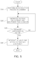
- FIG. 5 illustrates a flowchart of a method of controlling a semiconductor process according to an example embodiment.
- a method of controlling a semiconductor process may begin with performing a semiconductor process in a chamber included in the semiconductor processing equipment in operation S 10 .
- the semiconductor process as a process using plasma including radicals, ions, and the like, of a source gas, may be an etching process or a deposition process.
- a predetermined electrostatic chuck voltage may be supplied to the electrostatic chuck in the chamber, and bias power may be supplied to the bias electrodes in the chamber.
- the control device of the semiconductor processing equipment may detect an electrostatic chuck voltage and an electrostatic chuck current from the electrostatic chuck, and detect bias power supplied to the bias electrodes in operation S 20 .
- the control device may detect the electrostatic chuck voltage, the electrostatic chuck current, and the bias power in real time or once per predetermined period.
- the control device may determine whether an unintentional discharge has occurred between the wafer and the electrostatic chuck by comparing each of the electrostatic chuck voltage, the electrostatic chuck current, and the bias power with a reference value or a reference variation in operation S 30 .
- the control device may determine whether a discharge has occurred between the wafer and the electrostatic chuck by comparing two or more parameters among the electrostatic chuck voltage, the electrostatic chuck current, and the bias power with reference values, respectively. For example, when the electrostatic chuck voltage is reduced to below a reference voltage and the electrostatic chuck current is increased to be higher than a reference current, the control device may determine that a discharge has been generated between the wafer and the electrostatic chuck. Also, when the electrostatic chuck voltage is decreased to below the reference voltage and the bias power is increased to be higher than a reference power, the control device may determine that a discharge has been generated in helium.
- the control device may determine that a discharge has been generated between the wafer and the electrostatic chuck.
- the control device may provide a user interface for setting the reference voltage, the reference current, and the reference power to a manager of the semiconductor processing equipment.
- the control device may determine whether a discharge has occurred between the wafer and the electrostatic chuck by comparing variations of two or more parameters among the electrostatic chuck voltage, the electrostatic chuck current, and the bias power with a reference variation. For example, if a variation in the electrostatic chuck voltage is higher than a first reference variation and a variation in the electrostatic chuck current is higher than a second reference variation, the control device may determine that a discharge has been generated between the wafer and the electrostatic chuck. Also, if the electrostatic chuck voltage is higher than the second reference variation and a variation in the bias power is higher than a third reference variation, the control device may determine that a discharge has been generated in helium.
- control device may determine that a discharge has been generated between the wafer and the electrostatic chuck.
- the control device may provide a user interface for setting the first to third reference variations to the manager of the semiconductor processing equipment.
- An inert gas such as helium (He), or the like, may be injected between the wafer and the electrostatic chuck for the purpose of cooling the wafer.
- the control device may interrupt at least one of the electrostatic chuck voltage and the bias power or shut down the semiconductor processing equipment in operation S 40 . Meanwhile, if it is not determined in step S 30 that a discharge has been occurred between the wafer and the electrostatic chuck, the control device may continue to detect the electrostatic chuck voltage, the electrostatic chuck current, and the bias power, without taking any protective measures.
- the method of controlling a semiconductor process described above with reference to FIG. 5 may be realized by software executable in the control device of the semiconductor processing equipment or hardware installed in the control device.
- the electrostatic chuck voltage, the electrostatic chuck current, the bias power, and the like are values which are generally monitored in the chamber in which an etching process or a deposition process using plasma is performed.
- aspects of the method of controlling a semiconductor process according to an example embodiment may be implemented in software on the control device.
- FIG. 6 and FIG. 7 illustrate circuit diagrams provided to explain a method of controlling a semiconductor process according to an example embodiment.
- a discharge detection circuit 400 includes first to third comparators 401 to 403 , first to third AND gates 404 to 406 , and an OR gate 407 .
- the first to third comparators 401 to 403 may compare an electrostatic chuck voltage V ESC , an electrostatic chuck current I ESC , and bias power P BIAS with a reference voltage V REF , a reference current I REF , and reference power P REF , respectively.
- the first comparator 401 may output a high logic value if the electrostatic chuck voltage V ESC decreases to be lower than the reference voltage V REF .
- the second comparator 402 may output a high logic value if the electrostatic chuck current I ECS increases to be equal to or greater than the reference current I REF .
- the third comparator 403 may output a high logic value if the bias power P BIAS increases to be higher than the reference power P REF .
- the first AND gate 404 may output a high logic value when both the first comparator 401 and the second comparator 402 output a high logic value. Thus, if the electrostatic chuck voltage V ESC decreases to be lower than the reference voltage V REF and the electrostatic chuck current I ESC increases to be higher than the reference current I REF , the first AND gate 404 may output a high logic value.
- the second AND gate 405 may output a high logic value when both the second comparator 402 and the third comparator 403 output a high logic value. Thus, if the electrostatic chuck current I ESC increases to be higher than the reference current I REF and the bias power P BIAS increases to be higher than the reference power P REF , the second AND gate 405 may output a high logic value.
- the third AND gate 406 may output a high logic value when both the third comparator 403 and the first comparator 401 output a high logic value. Thus, if the bias power P BIAS increases to be higher than the reference power P REF and the electrostatic chuck voltage V ESC decreases to be lower than the reference voltage V REF , the third AND gate 406 may output a high logic value.
- the output signal OUT of the OR gate 407 may have a high logic value when any one of the first to third AND gates 404 to 406 has a high logic value.
- An output terminal of the OR gate 407 may be connected to a power switch of a chuck voltage supplier and/or a bias power supplier.
- the power switch of the chuck voltage supplier and/or the bias power supplier may be turned off when an output signal OUT of the OR gate 407 has a high logic value.
- the output terminal of the OR gate 407 may be connected to a power switch of the chamber included in the semiconductor processing equipment, and when the output signal OUT of the OR gate 407 has a high logic value, the power switch of the chamber may be turned off.
- a discharge detection circuit 410 may include first to third comparators 411 to 413 , first to third AND gates 414 to 416 , and an OR gate 417 .
- the first to third comparators 401 to 403 may compare a variation ⁇ V ESC of an electrostatic chuck voltage, a variation ⁇ I ESC of an electrostatic chuck current, and a variation ⁇ P BIAS of bias power with a first reference variation ⁇ V REF , a second reference variation ⁇ I REF , and a third reference variation ⁇ P REF , respectively.
- the first comparator 411 may output a high logic value if the variation ⁇ V ESC of the electrostatic chuck voltage is higher than the first reference variation ⁇ V REF
- the second comparator 412 may output a high logic value if the variation ⁇ I ESC of the electrostatic chuck current is higher than the second reference variation ⁇ I REF
- the third comparator 413 may output a high logic value if the variation ⁇ P BIAS of the bias power is higher than the third reference variation ⁇ P REF .
- the first AND gate 414 may output a high logic value when both the first comparator 411 and the second comparator 412 output a high logic value. Thus, if the variation ⁇ V ESC of the electrostatic chuck voltage is higher than the first reference variation ⁇ V REF and the variation ⁇ I ESC of the electrostatic chuck current is higher than the second reference variation ⁇ I REF , the first AND gate 414 may output a high logic value.
- the second AND gate 415 may output a high logic value when both the second comparator 412 and the third comparator 413 output a high logic value.
- the second AND gate 415 may output a high logic value when the variation ⁇ I ESC of the electrostatic chuck current is higher than the second reference variation ⁇ I REF and the variation ⁇ P BAIS of the bias power is higher than the third reference variation ⁇ P REF .
- the third AND gate 416 may output a high logic value when both the third comparator 413 and the first comparator 411 output a high logic value.
- the third AND gate 416 may output a high logic value if the variation ⁇ P BIAS of the bias power is higher than the third reference variation ⁇ P REF and the variation ⁇ V ESC of the electrostatic chuck voltage is higher than the first reference variation ⁇ V REF .
- the output signal OUT of the OR gate 417 may have a high logic value when any one of the first to third AND gates 414 to 416 has a high logic value.
- An output terminal of the OR gate 417 may be connected to a power switch of a chuck voltage supplier, a bias power supplier, and/or the chamber.
- the power switch of the chuck voltage supplier, the bias power supplier, and/or the chamber may be turned off when the output signal OUT has a high logic value.
- the semiconductor processing equipment may include one or more of the discharge detection circuits 400 and 410 according to the example embodiments described above with reference to FIGS. 6 and 7 .
- the output signal OUT of each of the discharge detection circuits 400 and 410 may be input to the single OR gate.
- the output terminal of the OR gate may be connected to the power switch of the chuck voltage supplier, the bias power supplier, and/or the chamber, and when the output signal of the OR gate has a high logic value, the power switch of the chuck voltage supplier, the bias power supplier, and/or the chamber may be turned off.
- FIG. 8 illustrates a view of semiconductor processing equipment to which a semiconductor process control method according to an example embodiment may be applied.
- a semiconductor processing equipment 500 may include a plurality of chambers 510 to 540 .
- the plurality of chambers 510 to 540 may receive a wafer through a transfer chamber 501 and a load lock chamber 502 and perform a semiconductor process.
- at least one of the plurality of chambers 510 to 540 may be a plasma processing chamber that generates plasma containing radicals and ions of a source gas to conduct an etching or deposition process.
- a transfer robot may be provided inside the transfer chamber 501 , and the transfer robot may transfer wafers to the load lock chamber 502 .
- the load lock chamber 502 may also include a transfer robot, and the transfer robot may transfer wafers to the plurality of chambers 510 to 540 or shift wafers between the plurality of chambers 510 to 540 .
- a control device 550 may monitor operations of the plurality of chambers 510 to 540 , the transfer chamber 501 , and the load lock chamber 502 .
- the control device 550 may detect an electrostatic chuck current from the electrostatic chuck while monitoring an electrostatic chuck voltage, bias power, and the like, supplied to the plasma processing chamber, among the plurality of chambers 510 to 540 .
- the control device 550 may compare the electrostatic chuck voltage, the electrostatic chuck current, and/or the bias power with a reference value or compare a variation in the electrostatic chuck voltage, a variation in the electrostatic chuck current, and/or a variation in the bias power with a reference variation.
- the control device 550 may interrupt supply of the electrostatic chuck voltage and/or bias power on the basis of a result of the comparison, or stop an operation of the chamber (among the plurality of chambers 510 to 540 ) in which a rapid change in the electrostatic chuck voltage, the electrostatic chuck current, and/or the bias power is detected.
- the rapid change in the electrostatic chuck voltage, electrostatic chuck current, and/or bias power may indicate that an unintentional discharge has been generated in an inert gas, for example, helium (He), or the like, injected between the electrostatic chuck and the wafer in the chamber.
- an inert gas for example, helium (He), or the like
- the control device 550 may stop the operation of the chamber in which the rapid change in the electrostatic chuck voltage, the electrostatic chuck current, and/or the bias power is detected, or interrupt the electrostatic chuck voltage and/or the bias power supplied to the chamber to protect the chamber and the wafer.
- FIGS. 9A, 9B, and 10 are graphs provided to illustrate a method of controlling a semiconductor process according to an example embodiment.
- FIG. 9A is a graph illustrating an electrostatic chuck current detected from the electrostatic chuck when no discharge was generated in an inert gas injected between the electrostatic chuck and the wafer inside the chamber.
- FIG. 9B is a graph illustrating an electrostatic chuck current detected when a discharge was generated in the inert gas injected between the electrostatic chuck and the wafer inside the chamber.
- the electrostatic chuck current has a relatively stable value over time.
- FIG. 9B (for the case when a discharge was generated in the inert gas), it can be seen that the electrostatic chuck current repeatedly increases and decreases with reference to a central value, fluctuating significantly.
- the semiconductor processing equipment may determine whether a discharge has occurred in the inert gas injected between the electrostatic chuck and the wafer in the chamber by detecting the increase or decrease in the electrostatic chuck current.
- FIG. 10 is a graph illustrating changes in an electrostatic chuck voltage, an electrostatic chuck current, and a bias power when a discharge has occurred in an inert gas injected between the electrostatic chuck and the wafer in a chamber.
- the bias power and the electrostatic chuck current increase and the electrostatic chuck voltage decreases in the vicinity of a process time of about 9 minutes and 50 seconds.
- generation of the discharge in the inert gas injected between the electrostatic chuck and the wafer in the chamber may lead to the increase in the electrostatic chuck current and bias power and the decrease in the electrostatic chuck voltage.
- whether a discharge occurred in an inert gas injected between the electrostatic chuck and the wafer in the chamber may be quickly detected by detecting at least one of an electrostatic chuck voltage, an electrostatic chuck current, and a bias power and comparing the detected voltage, current, or power with a reference value or a reference variation. Also, when a discharge of the inert gas is detected, the electrostatic chuck voltage and/or bias power supplied to the chamber may be shut off. Therefore, the wafer and the chamber may be effectively protected by automatically detecting a discharge of the inert gas and stopping the process, without a separate checking operation by an operator.
- radicals and ions may be formed inside the chamber.
- the radicals and ions may be formed by bias power supplied to the chamber.
- embodiments may provide a method of controlling a semiconductor process that detects a discharge in an inert gas that may occur between a wafer and an electrostatic chuck during a dry etching process.
- whether a discharge has occurred between the wafer and the electrostatic chuck may be determined by detecting a voltage or a current in various positions inside the chamber in which the semiconductor process is performed using plasma and comparing the detected voltage or current with a reference value. Therefore, generation of a discharge may be effectively detected, and when a discharge has occurred, a voltage supplied to the electrostatic chuck or bias power supplied to the chamber may be interrupted, effectively protecting the wafer and the electrostatic chuck.
Landscapes
- Physics & Mathematics (AREA)
- Engineering & Computer Science (AREA)
- Plasma & Fusion (AREA)
- Chemical & Material Sciences (AREA)
- Analytical Chemistry (AREA)
- Spectroscopy & Molecular Physics (AREA)
- Container, Conveyance, Adherence, Positioning, Of Wafer (AREA)
- Drying Of Semiconductors (AREA)
Abstract
Description
Claims (19)
Applications Claiming Priority (2)
| Application Number | Priority Date | Filing Date | Title |
|---|---|---|---|
| KR10-2017-0179064 | 2017-12-26 | ||
| KR1020170179064A KR102524810B1 (en) | 2017-12-26 | 2017-12-26 | Method for controlling semiconductor process |
Publications (2)
| Publication Number | Publication Date |
|---|---|
| US20190198373A1 US20190198373A1 (en) | 2019-06-27 |
| US11049754B2 true US11049754B2 (en) | 2021-06-29 |
Family
ID=66949646
Family Applications (1)
| Application Number | Title | Priority Date | Filing Date |
|---|---|---|---|
| US16/031,321 Active 2039-07-08 US11049754B2 (en) | 2017-12-26 | 2018-07-10 | Method for controlling semiconductor process |
Country Status (2)
| Country | Link |
|---|---|
| US (1) | US11049754B2 (en) |
| KR (1) | KR102524810B1 (en) |
Citations (15)
| Publication number | Priority date | Publication date | Assignee | Title |
|---|---|---|---|---|
| US5665166A (en) * | 1993-01-29 | 1997-09-09 | Tokyo Electron Limited | Plasma processing apparatus |
| US20040031699A1 (en) * | 2002-08-19 | 2004-02-19 | Applied Materials, Inc. | Method for performing real time arcing detection |
| US20040228055A1 (en) * | 2003-05-16 | 2004-11-18 | Ballard Power Systems Inc. | Power supplies and ultracapacitor based battery simulator |
| JP2006210726A (en) | 2005-01-28 | 2006-08-10 | Hitachi High-Technologies Corp | Plasma processing method and plasma processing apparatus |
| US7514936B2 (en) | 2004-09-04 | 2009-04-07 | Applied Materials, Inc. | Detection and suppression of electrical arcing |
| US7915563B2 (en) | 2006-09-28 | 2011-03-29 | Daihen Corporation | Arc detector for plasma processing system |
| US7974067B2 (en) | 2005-09-06 | 2011-07-05 | Renesas Electronics Corporation | Plasma processing apparatus and method of suppressing abnormal discharge therein |
| US20120175060A1 (en) | 2008-05-12 | 2012-07-12 | Lam Research Corporation | Detection of arcing events in wafer plasma processing through monitoring of trace gas concentrations |
| KR20120110677A (en) | 2011-03-30 | 2012-10-10 | 엘아이지에이디피 주식회사 | Plasma processing apparatus |
| US20120308341A1 (en) * | 2009-11-09 | 2012-12-06 | Tokyo Electron Limited | Substrate processing apparatus and method of controlling substrate processing apparatus |
| KR20140101451A (en) | 2012-12-06 | 2014-08-20 | (주)화백엔지니어링 | Plasma monitoring apparatus |
| JP2015170437A (en) | 2014-03-06 | 2015-09-28 | Sppテクノロジーズ株式会社 | Abnormal discharge prediction method and device of plasma processing apparatus; and plasma processing apparatus with abnormal discharge prediction function |
| US9170295B2 (en) | 2012-02-28 | 2015-10-27 | New Power Plasma Co., Ltd. | Method and apparatus for detecting arc in plasma chamber |
| US20160268108A1 (en) | 2009-08-17 | 2016-09-15 | Verity Instruments, Inc. | Method and apparatus for the detection of arc events during the plasma processing of a wafer, surface of substrate |
| US20170077002A1 (en) | 2012-03-15 | 2017-03-16 | Applied Materials, Inc. | System to detect wafer arcing in semiconductor manufacturing equipment |
Family Cites Families (2)
| Publication number | Priority date | Publication date | Assignee | Title |
|---|---|---|---|---|
| JP3664745B2 (en) * | 1994-03-01 | 2005-06-29 | 富士通株式会社 | Substrate processing apparatus and method |
| JP3907256B2 (en) * | 1997-01-10 | 2007-04-18 | 芝浦メカトロニクス株式会社 | Electrostatic chuck device for vacuum processing equipment |
-
2017
- 2017-12-26 KR KR1020170179064A patent/KR102524810B1/en active Active
-
2018
- 2018-07-10 US US16/031,321 patent/US11049754B2/en active Active
Patent Citations (17)
| Publication number | Priority date | Publication date | Assignee | Title |
|---|---|---|---|---|
| US5665166A (en) * | 1993-01-29 | 1997-09-09 | Tokyo Electron Limited | Plasma processing apparatus |
| US20040031699A1 (en) * | 2002-08-19 | 2004-02-19 | Applied Materials, Inc. | Method for performing real time arcing detection |
| US20040228055A1 (en) * | 2003-05-16 | 2004-11-18 | Ballard Power Systems Inc. | Power supplies and ultracapacitor based battery simulator |
| US7514936B2 (en) | 2004-09-04 | 2009-04-07 | Applied Materials, Inc. | Detection and suppression of electrical arcing |
| JP2006210726A (en) | 2005-01-28 | 2006-08-10 | Hitachi High-Technologies Corp | Plasma processing method and plasma processing apparatus |
| US7224568B2 (en) | 2005-01-28 | 2007-05-29 | Hitachi High-Technologies Corporation | Plasma processing method and plasma processing apparatus |
| JP5094002B2 (en) | 2005-09-06 | 2012-12-12 | ルネサスエレクトロニクス株式会社 | Plasma processing apparatus and method for suppressing abnormal discharge thereof |
| US7974067B2 (en) | 2005-09-06 | 2011-07-05 | Renesas Electronics Corporation | Plasma processing apparatus and method of suppressing abnormal discharge therein |
| US7915563B2 (en) | 2006-09-28 | 2011-03-29 | Daihen Corporation | Arc detector for plasma processing system |
| US20120175060A1 (en) | 2008-05-12 | 2012-07-12 | Lam Research Corporation | Detection of arcing events in wafer plasma processing through monitoring of trace gas concentrations |
| US20160268108A1 (en) | 2009-08-17 | 2016-09-15 | Verity Instruments, Inc. | Method and apparatus for the detection of arc events during the plasma processing of a wafer, surface of substrate |
| US20120308341A1 (en) * | 2009-11-09 | 2012-12-06 | Tokyo Electron Limited | Substrate processing apparatus and method of controlling substrate processing apparatus |
| KR20120110677A (en) | 2011-03-30 | 2012-10-10 | 엘아이지에이디피 주식회사 | Plasma processing apparatus |
| US9170295B2 (en) | 2012-02-28 | 2015-10-27 | New Power Plasma Co., Ltd. | Method and apparatus for detecting arc in plasma chamber |
| US20170077002A1 (en) | 2012-03-15 | 2017-03-16 | Applied Materials, Inc. | System to detect wafer arcing in semiconductor manufacturing equipment |
| KR20140101451A (en) | 2012-12-06 | 2014-08-20 | (주)화백엔지니어링 | Plasma monitoring apparatus |
| JP2015170437A (en) | 2014-03-06 | 2015-09-28 | Sppテクノロジーズ株式会社 | Abnormal discharge prediction method and device of plasma processing apparatus; and plasma processing apparatus with abnormal discharge prediction function |
Also Published As
| Publication number | Publication date |
|---|---|
| KR20190077685A (en) | 2019-07-04 |
| KR102524810B1 (en) | 2023-04-24 |
| US20190198373A1 (en) | 2019-06-27 |
Similar Documents
| Publication | Publication Date | Title |
|---|---|---|
| US11011351B2 (en) | Monoenergetic ion generation for controlled etch | |
| US8440061B2 (en) | System and method for plasma arc detection, isolation and prevention | |
| KR102069412B1 (en) | Systems and methods for detection of plasma instability by electrical measurement | |
| CN101772992B (en) | Abnormal discharge suppressing device for vacuum apparatus | |
| US9966291B2 (en) | De-chuck control method and plasma processing apparatus | |
| US7864502B2 (en) | In situ monitoring of wafer charge distribution in plasma processing | |
| US5948703A (en) | Method of soft-landing gate etching to prevent gate oxide damage | |
| US11456199B2 (en) | Measurement method and measuring jig | |
| US20250308969A1 (en) | Multi-modal electrostatic chucking | |
| TW201501236A (en) | Non-intrusive measurement of wafer DC self-bias in semiconductor processing equipment | |
| US10892146B2 (en) | Endpoint detecting method and endpoint detecting apparatus | |
| US11049754B2 (en) | Method for controlling semiconductor process | |
| US20150041060A1 (en) | Plasma processing apparatus | |
| KR102637282B1 (en) | Determination of semiconductor chamber operating parameters for the optimization of critical dimension uniformity | |
| US12431341B2 (en) | Apparatus for arcing diagnosis, plasma process equipment including the same, and arcing diagnosis method | |
| US6800562B1 (en) | Method of controlling wafer charging effects due to manufacturing processes | |
| US8293649B2 (en) | Release accumulative charges on wafers using O2 neutralization | |
| US8186300B2 (en) | Plasma processing apparatus | |
| US8263495B2 (en) | Release accumulative charges by tuning ESC voltages in via-etchers | |
| KR102577288B1 (en) | Apparatus for treating substrate and method thereof | |
| JP2005236053A (en) | Plasma processing method and plasma processing apparatus | |
| JP3946467B2 (en) | Dry etching method | |
| Karzhavin et al. | Plasma-induced charging evaluation using SCA and PDM tools | |
| WO2026019766A1 (en) | High aspect ratio plasma etching with controlled declogging | |
| KR20240090369A (en) | Systems and methods for determining phase difference between RF signals provided to electrodes |
Legal Events
| Date | Code | Title | Description |
|---|---|---|---|
| AS | Assignment |
Owner name: SAMSUNG ELECTRONICS CO., LTD., KOREA, REPUBLIC OF Free format text: ASSIGNMENT OF ASSIGNORS INTEREST;ASSIGNORS:MYUNG, SEUL HA;PARK, MIN JOON;KIM, HYO SUNG;AND OTHERS;SIGNING DATES FROM 20180605 TO 20180625;REEL/FRAME:046306/0544 |
|
| FEPP | Fee payment procedure |
Free format text: ENTITY STATUS SET TO UNDISCOUNTED (ORIGINAL EVENT CODE: BIG.); ENTITY STATUS OF PATENT OWNER: LARGE ENTITY |
|
| STPP | Information on status: patent application and granting procedure in general |
Free format text: RESPONSE TO NON-FINAL OFFICE ACTION ENTERED AND FORWARDED TO EXAMINER |
|
| STPP | Information on status: patent application and granting procedure in general |
Free format text: NOTICE OF ALLOWANCE MAILED -- APPLICATION RECEIVED IN OFFICE OF PUBLICATIONS |
|
| STPP | Information on status: patent application and granting procedure in general |
Free format text: AWAITING TC RESP., ISSUE FEE NOT PAID |
|
| STPP | Information on status: patent application and granting procedure in general |
Free format text: NOTICE OF ALLOWANCE MAILED -- APPLICATION RECEIVED IN OFFICE OF PUBLICATIONS |
|
| STPP | Information on status: patent application and granting procedure in general |
Free format text: PUBLICATIONS -- ISSUE FEE PAYMENT RECEIVED |
|
| STPP | Information on status: patent application and granting procedure in general |
Free format text: PUBLICATIONS -- ISSUE FEE PAYMENT VERIFIED |
|
| STCF | Information on status: patent grant |
Free format text: PATENTED CASE |
|
| MAFP | Maintenance fee payment |
Free format text: PAYMENT OF MAINTENANCE FEE, 4TH YEAR, LARGE ENTITY (ORIGINAL EVENT CODE: M1551); ENTITY STATUS OF PATENT OWNER: LARGE ENTITY Year of fee payment: 4 |