US11048654B2 - Systems and methods for providing multiple memory channels with one set of shared address pins on the physical interface - Google Patents
Systems and methods for providing multiple memory channels with one set of shared address pins on the physical interface Download PDFInfo
- Publication number
- US11048654B2 US11048654B2 US16/169,525 US201816169525A US11048654B2 US 11048654 B2 US11048654 B2 US 11048654B2 US 201816169525 A US201816169525 A US 201816169525A US 11048654 B2 US11048654 B2 US 11048654B2
- Authority
- US
- United States
- Prior art keywords
- channel
- command
- address
- controller
- memory
- Prior art date
- Legal status (The legal status is an assumption and is not a legal conclusion. Google has not performed a legal analysis and makes no representation as to the accuracy of the status listed.)
- Active, expires
Links
Images


Classifications
-
- G—PHYSICS
- G06—COMPUTING OR CALCULATING; COUNTING
- G06F—ELECTRIC DIGITAL DATA PROCESSING
- G06F13/00—Interconnection of, or transfer of information or other signals between, memories, input/output devices or central processing units
- G06F13/14—Handling requests for interconnection or transfer
- G06F13/16—Handling requests for interconnection or transfer for access to memory bus
- G06F13/1668—Details of memory controller
- G06F13/1689—Synchronisation and timing concerns
-
- G—PHYSICS
- G06—COMPUTING OR CALCULATING; COUNTING
- G06F—ELECTRIC DIGITAL DATA PROCESSING
- G06F1/00—Details not covered by groups G06F3/00 - G06F13/00 and G06F21/00
- G06F1/04—Generating or distributing clock signals or signals derived directly therefrom
- G06F1/12—Synchronisation of different clock signals provided by a plurality of clock generators
-
- G—PHYSICS
- G06—COMPUTING OR CALCULATING; COUNTING
- G06F—ELECTRIC DIGITAL DATA PROCESSING
- G06F13/00—Interconnection of, or transfer of information or other signals between, memories, input/output devices or central processing units
- G06F13/14—Handling requests for interconnection or transfer
- G06F13/16—Handling requests for interconnection or transfer for access to memory bus
- G06F13/1668—Details of memory controller
- G06F13/1694—Configuration of memory controller to different memory types
-
- G—PHYSICS
- G11—INFORMATION STORAGE
- G11C—STATIC STORES
- G11C7/00—Arrangements for writing information into, or reading information out from, a digital store
- G11C7/10—Input/output [I/O] data interface arrangements, e.g. I/O data control circuits, I/O data buffers
- G11C7/1075—Input/output [I/O] data interface arrangements, e.g. I/O data control circuits, I/O data buffers for multiport memories each having random access ports and serial ports, e.g. video RAM
-
- G—PHYSICS
- G06—COMPUTING OR CALCULATING; COUNTING
- G06F—ELECTRIC DIGITAL DATA PROCESSING
- G06F13/00—Interconnection of, or transfer of information or other signals between, memories, input/output devices or central processing units
- G06F13/14—Handling requests for interconnection or transfer
- G06F13/20—Handling requests for interconnection or transfer for access to input/output bus
- G06F13/28—Handling requests for interconnection or transfer for access to input/output bus using burst mode transfer, e.g. direct memory access DMA, cycle steal
- G06F13/287—Multiplexed DMA
-
- Y—GENERAL TAGGING OF NEW TECHNOLOGICAL DEVELOPMENTS; GENERAL TAGGING OF CROSS-SECTIONAL TECHNOLOGIES SPANNING OVER SEVERAL SECTIONS OF THE IPC; TECHNICAL SUBJECTS COVERED BY FORMER USPC CROSS-REFERENCE ART COLLECTIONS [XRACs] AND DIGESTS
- Y02—TECHNOLOGIES OR APPLICATIONS FOR MITIGATION OR ADAPTATION AGAINST CLIMATE CHANGE
- Y02D—CLIMATE CHANGE MITIGATION TECHNOLOGIES IN INFORMATION AND COMMUNICATION TECHNOLOGIES [ICT], I.E. INFORMATION AND COMMUNICATION TECHNOLOGIES AIMING AT THE REDUCTION OF THEIR OWN ENERGY USE
- Y02D10/00—Energy efficient computing, e.g. low power processors, power management or thermal management
Definitions
- the disclosure herein relates to memory interface, particularly relates to multi-channel memory interface architecture.
- Computing systems need to use storage medium to maintain and store data and instructions.
- storage medium There are typically two types of storage medium: volatile and non-volatile.
- Volatile storage such as Random Access Memory (RAM)
- RAM Random Access Memory
- non-volatile storage such as floppy disks, hard drives, magnetic tapes, optical discs, maintains its state even if power is interrupted.
- RAM Random Access Memory
- non-volatile storage such as floppy disks, hard drives, magnetic tapes, optical discs, maintains its state even if power is interrupted.
- RAM Random Access Memory
- non-volatile storage such as floppy disks, hard drives, magnetic tapes, optical discs
- These two types of storage are typically accessed via different interfacing technologies that vary significantly and are generally incompatible.
- Recent development of new storage and memory technologies normally packs more and more storage medium modules into one computing system.
- a modern storage controller is usually configured to support multiple channels to access multiple storage units.
- a multi-channel memory interface architecture has to have the necessary interface to communicate with multiple storage units. But the physical interface of such an architecture is a valuable resource because the space for connection pins is limited. Moreover, recent development in non-volatile memory is providing more and more advanced memory media, which is different from the traditional RAM and traditional non-volatile storage. Therefore, there is a need in the art for improved multi-channel memory interface architecture design, to utilize the advanced new memory media features.
- the disclosed subject matter relates to systems, methods, and devices that combines multiple channels in a memory controller.
- the provided techniques may share an address/command (AD/CMD) bus among a plurality of memory channels whereas each channel may have a separate data bus.
- the exemplary memory controllers may be implemented in a stand-alone memory controller, such as a DRAM controller of a computing system, or as part of a storage controller, such as a solid state drive (SSD) controller.
- SSD solid state drive
- an apparatus comprising: a first memory controller configured to access a first channel using a first protocol; a second memory controller configured to access a second channel using a second protocol that is different from the first protocol; and a physical interface coupled to the first memory controller and a second memory controller.
- the physical interface comprises a set of pins for an address and command bus shared by the first memory controller and the second memory controller for the first memory controller and the second memory controller to send address or command to respective channels.
- a method comprising: receiving a first command from a first channel controller of a multi-channel memory controller at a physical interface of the multi-channel memory controller; receiving a second command from a second channel controller of the multi-channel memory controller at the physical interface.
- the first command may be a command of a first protocol and the second command may be a command of a second protocol, and the first memory protocol may be different from the second memory protocol.
- the method may further comprise sending the first command during a first time slot from the physical interface via a set of pins to a first memory module of a first memory type; and sending the second command during a second time slot from the physical interface via the set of pins to a second memory module of a second memory type.
- the set of pins may be shared by the first channel and second channel.
- the first protocol and the second protocol may be compatible protocols.
- a non-transitory machine-readable medium having information, which when read by a hardware processor system, causes the hardware processor system to perform: receiving a first command from a first channel controller of a multi-channel memory controller at a physical interface of the multi-channel memory controller; receiving a second command from a second channel controller of the multi-channel memory controller at the physical interface; sending the first command during a first time slot from the physical interface via a set of pins to a first memory module of a first memory type; and sending the second command during a second time slot from the physical interface via the set of pins to a second memory module of a second memory type.
- the first command may be a command of a first protocol and the second command may be a command of a second protocol, and the first memory protocol may be different from the second memory protocol.
- the set of pins may be shared by the first channel and second channel.
- FIG. 1A schematically shows a memory controller with a multi-channel memory interface architecture in accordance with an embodiment of the present disclosure.
- FIG. 1B schematically shows a multi-channel memory interface architecture in accordance with another embodiment of the present disclosure.
- FIG. 2 schematically shows signals on various signal lines in a multi-channel storage system in accordance with an embodiment of the present disclosure.
- FIG. 3 schematically shows signals on various signal lines in a multi-channel storage system in accordance with another embodiment of the present disclosure.
- FIG. 4 schematically shows signals on various signal lines in a multi-channel storage system in accordance with yet another embodiment of the present disclosure.
- FIG. 5 is a flowchart for operating a multi-channel memory controller in accordance with an embodiment of the present disclosure.
- An exemplary memory controller may implement a multi-channel memory interface architecture to provide support for two or more channels. Each channel may be independent by having a respective dedicated data bus and being controlled independently. Multiple channels, however, may share a single address and command bus.
- a memory controller may have a physical interface (PHY) configured with multiple channels for multiple memory modules. Each memory module may be a memory unit for storing data and instructions.
- PHY physical interface
- the memory modules that may be coupled to the channels may include, for example, Synchronous Dynamic Random Access Memory (SDRAM), Double Data Rate SDRAM (DDR), DDR version 2 (DDR2) SDRAM (DDR2), DDR version 3 SDRAM (DDR3), DDR version 4 SDRAM (DDR4), NAND flash memories, NOR flash memories, Magnetoresistive Random Access Memory (MRAM), Resistive Random Access Memory (RRAM), Phase Change Random Access Memory (PCRAM), Nano-RAM, 3D XPoint memory, etc.
- SDRAM Synchronous Dynamic Random Access Memory
- DDR Double Data Rate SDRAM
- DDR2 SDRAM DDR version 2 SDRAM
- DDR3 SDRAM DDR version 3 SDRAM
- DDR4 SDRAM DDR4
- NAND flash memories NOR flash memories
- MRAM Magnetoresistive Random Access Memory
- RRAM Resistive Random Access Memory
- PCRAM Phase Change Random Access Memory
- Nano-RAM 3D XPoint memory
- a memory system may have a total data bus width that may not be power of 2.
- the total data bus width may be 48-bit, which may be a 32-bit data bus for one channel combined with a 16-bit data bus for another channel.
- different memory types may be combined to form a flexible memory system. For example, one channel may be configured for DRAM and another channel may be configured for MRAM, or one channel may be configured for DDR3 and another channel may be configured for DDR4.
- FIG. 1A schematically shows a memory controller 102 with a multi-channel memory interface architecture in accordance with an embodiment of the present disclosure.
- the memory controller 102 may comprise a physical interface 104 , a first channel controller 114 , a second channel controller 120 , a first data bus 112 , a second data bus 126 and an address bus 128 .
- the first channel controller 114 may provide a first channel, denoted as CH A, to the memory controller 102 .
- the first channel controller 114 may comprise a data path component 116 and an address component 118 .
- the data path component 116 may be configured to handle data to be written to and/or received from a memory module (not shown) attached to the first channel.
- the data path component 116 may be coupled to a first set of data pins 106 of the physical interface 104 via the first data bus 112 .
- the first set of data pins 106 may be coupled to the memory module attached to the first channel via an external data bus (not shown).
- the address component 118 may be configured to specify the address (where on the memory module the data to be written to or read from) and issue any commands to the first channel.
- the address component 118 may also be referred to as an address/command component.
- the address component 118 may be coupled to a set of address/command pins 110 of the physical interface 104 via the address bus 128 .
- the set of address/command pins 110 of the physical interface 104 may also be referred to as the address PHY.
- the address bus 128 may also be used for transferring commands, it may also be referred to as an address/command (AD/CMD) bus.
- the second channel controller 120 may provide a second channel, denoted as CH B, to the memory controller 102 .
- the second channel controller 120 may comprise a data path component 122 and an address component 124 .
- the data path component 122 may be configured to handle data to be written to and/or received from a memory module (not shown) attached to the second channel.
- the data path component 122 may be coupled to a second set of data pins 108 of the physical interface 104 via the second data bus 126 .
- the second set of data pins 108 may be coupled to the memory module attached to the second channel via another external data bus (not shown).
- the address component 124 may be configured to specify the address (where on the memory module the data to be written to or read from) and issue any commands to the second channel.
- the address component 124 may also be referred to as an address/command component. Moreover, the address component 124 may also be coupled to the set of address/command pins 110 of the physical interface 104 via the address bus 128 . That is, the address bus 128 may be shared by first channel controller 114 and the second channel controller 120 .
- the first channel controller 114 may be configured according to a first protocol and the second channel controller 120 may be configured according to a second protocol.
- a protocol may refer to a standard or specification that defines how a memory module (e.g., a memory chip) may be accessed.
- the memory module attached to each of the first channel controller 114 and second channel controller 120 may be a corresponding memory type.
- Each of the first protocol and the second protocol may be one of a known memory protocol, such as but not limited to, SDRAM, DDR, DDR2, DDR3, DDR4, NAND, NOR, MRAM, RRAM, PCRAM, Nano-RAM, or 3D XPoint, or any future developed memory protocol.
- the first protocol may be different from the second protocol.
- the first protocol may be different from the second protocol but similar.
- general DDR-SDRAM protocols such as DDR3 and DDR4 may be protocol-compatible with each other, and thus in an embodiment, the first protocol may be DDR3 with the memory module attached to the first channel being a DDR3 memory module and the second protocol may be DDR4 with the memory module attached to the first channel being a DDR4 memory module.
- MRAM may be pin interface-compatible with general DDR-SDRAM protocols such as DDR3 and DDR4, and thus in another embodiment, the first protocol may be SDRAM with the memory module attached to the first channel being a SDRAM memory module and the second protocol may be MRAM with the memory module attached to the first channel being a MRAM memory module.
- pin interface-compatible may mean that a same set of physical pins may be used by both protocol, but the function of each pin may be the same or different for each memory module. Therefore, embodiments according to the present disclosure may share one set of address pins via a time division multiplexing scheme for a plurality types of memory modules attached to one external data bus.
- the time division multiplexing scheme may be implemented such that each clock cycle of the physical interface 104 may be designated for a specific channel. For example, channel A may be designated to use even clock cycles and channel B may be designated to use odd clock cycles.
- FIG. 1A shows a memory controller 102 shows two channels
- one or more additional channels may be added such that each additional channel may have a dedicated data bus but share the same set of address pins 110 of the physical interface 104 . Accordingly, a multi-channel memory interface architecture according to embodiments of the present disclosure may save physical space on the physical interface.
- the address pins 110 of physical interface 104 may be coupled to the address component 118 of the first channel controller 114 and address component 124 of the second channel component 120 via the shared address bus 128 . That is, the same set of address pins 110 may be shared by the first channel controller 114 and the second channel controller 120 . In an embodiment, one address pin may be mapped to same usage for all channels sharing the address bus. For example, a bank address zero (BA0) pin of the physical interface 104 may be mapped to BA0 outputs of both the first channel controller 114 and the second channel controller 120 .
- BA0 bank address zero
- FIG. 1B schematically shows a memory controller 102 A having a multi-channel memory interface architecture in accordance with another embodiment of the present disclosure.
- the memory controller 102 A may comprise a first channel controller 114 and a second channel controller 120 A, and a physical interface 104 A.
- the first channel controller 114 may be the same as in FIG. 1A .
- the second channel controller 120 A may be different from the second channel controller 120 in that at least some of the address outputs of the second channel controller 120 A may be different and need to be mapped to pins at the physical interface 104 A that may have a different usage as that for the first channel controller 114 .
- the physical interface 104 A may be different from the physical interface 104 in that the at least some connections to the channel controllers may not be shared by the channel controllers. For simplicity, portions of the memory controller 102 that may be the same as the memory controller 102 may be omitted (e.g., the data components and connections).
- the physical interface 104 A may have an address BA0 input 146 for a first time slot (e.g., Time Slot 0), an address BA0 input 148 for a second time slot (e.g., Time Slot 1), and a set of address/command pins 110 .
- the set of address/command pins 110 may be the same as that of FIG. 1A but for illustration purpose it shows, as an example, how an address pin 150 (also may be referred to as an address pad) of the set of address/command pins 110 may be mapped for different usage for two different channels.
- the address pin 150 may be coupled to both address BA0 input 146 and address BA0 input 148 inside the physical interface 104 A.
- the first channel controller 114 for channel A may have an address BA0 output 142 coupled to the address BA0 input 146 of the physical interface 104 and the second channel controller 120 for channel B may have an address AD0 output 144 coupled to the address BA0 input 148 of the physical interface 104 .
- the set of address/command pins 110 may be coupled to a memory module 152 of a first memory type and a memory module 154 of a second memory type via an external address connection (e.g., an external bus).
- the address pad 150 may be coupled to an address pin BA0 156 of the memory module 152 and an address pin AD0 158 of the memory module 154 .
- channel A's BA0 may be connected through BA0 input, output, pin throughout a memory system.
- channel B may be a SDRAM channel that is different from the memory protocol of channel A.
- AD0 (address 0) of the channel B controller 120 may be instead connected to BA0 time slot 1 of the address PHY and then connected back to the AD0 pin of SDRAM channel B via the BA0 Pad of the address PHY. Therefore, by providing multiple different inputs mapped to a same address pin on the address PHY but to work in a time division multiplexing manner, the memory controller 102 A may facilitate memory types with different Input/Output (IO) pins to share the same address PHY.
- the mapping of the address PHY may also allow for more optimal PCB (printed circuit board) layout because there may be fewer pins to be routed on a PCB.
- time division multiplexing may be achieved by allocating designated clock cycles (e.g., odd or even) to different channels (e.g., different memory modules attached to the address PHY via the set of address/command pins 110 and one shared external address bus).
- time division multiplexing may be realized by using a chip select (may be referred to, but not limited to, as a chip/channel select/enable) signal.
- the physical interface e.g., 104 , 104 A
- each memory channel e.g., one memory module from multiple memory modules attached to the shared external address bus
- the signal of the chip select pin for one memory channel may be asserted to an active state to select this memory channel to accept the address and command transmitted via the shared external address bus. If the signal of a chip select pin is not asserted to an active state, the corresponding memory channel may ignore the signals on the shared external address bus.
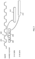
- FIG. 2 schematically shows signals on various signal lines in a multi-channel storage system in accordance with an embodiment of the present disclosure.
- a first read command RD_0 202 for a first channel may be issued (e.g., by the first channel controller 114 ) on a down phase 204 of a clock cycle of the physical interface (e.g., of the physical interface 104 or 104 A) via its address PHY
- a second read command RD_1 206 for a second channel may be issued on a down phase 208 of another clock cycle of the physical interface via the address PHY.
- the first channel may be the channel A of FIG. 1A or FIG.
- first external data bus (not shown) of a first width (e.g., 8, 12, 16, 32-bits) and data may be sent back from a memory module attached to the external data bus to the physical interface (e.g., the physical interface 104 or 104 A).
- the physical interface may in turn send the data to the channel controller 114 via a first internal data bus (e.g., data bus 112 ). As shown in FIG. 2 , the data may be transmitted over more than one clock cycle.
- the second channel may be the channel B of FIG. 1 that may have a second external data bus (not shown) of a second width (e.g., 8, 12, 16, 32-bits) and data may be sent back from a memory module attached to the second external data bus to the physical interface (e.g., the physical interface 104 or 104 A).
- the second width may be the same size as the first width of the first external bus in one embodiment, or a size different from the first width in another embodiment.
- the first external and internal data bus may be 32 bits
- the second external and internal data bus may be 8 bits or 16 bits.
- the data from the second external data bus may include data bits being transmitted over more than one clock cycle.
- the physical interface may in turn send the data to the channel controller 120 (or channel controller 120 A) via a second internal data bus (e.g., data bus 126 ). Because each of the channels have dedicated internal and external data buses, the time slots 210 and 212 for transmission of the data signals may overlap. But both read commands 202 and 206 may share the same set of address/command pins 110 .
- FIG. 3 schematically shows signals on various signal lines in a multi-channel storage system in accordance with another embodiment of the present disclosure.
- a time slot of the address PHY of a physical interface may be one half clock cycle of the physical interface.
- a first read command 302 for a first channel (e.g., CH A) may be issued on a down phase 304 of a clock cycle of the physical interface
- a second read command 304 for a second channel e.g., CH B
- Both read commands 302 and 306 may share the set of address/command pins 110 .
- the first channel and second channel may have dedicated internal and external data buses, and thus the time slots for transmission of the data signals 310 and 312 may overlap.
- FIG. 4 schematically shows signals on various signal lines in a multi-channel storage system in accordance with yet another embodiment of the present disclosure.
- a first channel controller e.g., channel controller 114
- a second channel controller e.g., channel controller 114 or 114 S
- the first channel clock may be twice as fast as the second channel clock.
- the physical interface clock for the address channel may be determined by the channel with highest frequency. As shown in FIG. 4 , the physical interface may operate at a clock frequency that have clock cycles 402 . 1 through 402 .
- Each of the clock cycles 402 . 1 through 402 . 2 may be one half of a clock cycle of the second channel clock.
- the first channel may have designated time slots that include two continuous PHY clock cycles (e.g., PHY clock cycles 402 . 1 - 402 . 2 , 402 . 5 - 402 . 6 , 402 . 9 - 402 . 10 ) and the second channel may have designated time slots that also include two continuous PHY clock cycles (e.g., PHY clock cycles 402 . 3 - 402 . 4 , 402 . 7 - 402 . 8 and 402 . 11 - 402 . 12 ).
- the memory modules may operate at different frequencies.
- Some PHY pins such as clock cannot be shared in this case.
- the physical interface may comprise a first clock pin for the first channel and a second clock pin for the second channel.
- the rising edge of channel B clock e.g., the clock signal line coupled to memory module of channel B
- the rising edge of channel A clock may be locked to every other falling edge of channel A clock (e.g., the clock signal line coupled to memory module of channel A).
- the first channel controller may issue two commands during a designated time slot. For example, during the PHY clock cycles 402 . 1 - 402 . 2 , the first channel controller may issue two commands: a write command 404 and a no-operation (NOP) command 406 ; and during the PHY clock cycles 402 . 5 - 402 . 6 , the first channel controller may issue two commands: a write command 410 and a NOP command 412 .
- NOP command may be special in that when the designated time slot has nothing to do, one NOP command, such as the NOP command 416 may occupy the whole designated time slot of PHY clock cycles 402 . 9 - 402 . 10 .
- the second channel controller may issue one command during a designated time slot of two PHY clock cycles. For example, during the PHY clock cycles 402 . 3 - 402 . 4 , the second channel controller may issue a write command 408 ; during the PHY clock cycles 402 . 7 - 402 . 8 , the second channel controller may issue a NOP command 414 ; and during the PHY clock cycles 402 . 11 - 402 . 12 , the second channel controller may issue a write command 418 .
- a read command may be replaced by a write command or any other commands
- a write command may be replaced by a read command or any other commands
- the address PHY may operate in the same time division multiplexing manner.
- An exemplary multi-channel memory controller may thus combine memories running at different frequencies and this may be achieved by combining channels running at a power-of-2 frequency ratio.
- the PHY clock for the address channel may be determined by the channel with highest frequency. Because different memory types may have different maximum operating frequencies, an embodiment may allow a faster memory type to run at or near its maximum frequency instead of being limited to a slower memory clock. In one embodiment, however, some sacrifice to the operating frequency may be required in order to match the frequency ratio.
- FIG. 5 is a flowchart of a process 500 for operating a multi-channel memory controller in accordance with an embodiment of the present disclosure.
- a first command from a first channel controller may be received at a physical interface.
- the first channel controller and the physical interface may be two components of the multi-channel memory controller.
- the physical interface 104 or 104 A of the memory controller 102 and 102 A may receive a first command (e.g., the read command 202 or 302 , or write command 404 ) from the first channel controller 114 .
- a second command from a second channel controller may be received at the physical interface.
- the second channel controller may be another component of the multi-channel memory controller.
- the physical interface 104 or 104 A of the memory controller 102 and 102 A may receive a second command (e.g., the read command 206 or 306 , or write command 408 ) from the second channel controller 120 or 120 A.
- the first command may be a command of a first protocol and the second command may be a command of a second protocol, and the first protocol may be different from the second protocol.
- the first channel controller may be configured for DDR3 and the second channel controller may be configured for DDR4 in an embodiment.
- a memory module used for the first channel may be a DDR3 memory module and a memory module used for the second channel may be a DDR4 memory module.
- the first protocol may be DDR3 and the second protocol may be DDR4.
- the first channel controller may be configured for SDRAM and the second channel controller may be configured for MRAM in another embodiment.
- a memory module used for the first channel may be a SDRAM memory module and a memory module used for the second channel may be a MRAM memory module.
- the first protocol may be SDRAM and the second protocol may be MRAM.
- the first command may be sent from the physical interface to a first memory module of a first memory type during a first time slot via a set of pins.
- the second command may be sent from the physical interface to a second memory module of a second memory type during a second time slot via the set of pins.
- one set of pins (e.g., the set of address/command pins 110 ) of the physical interface may be shared among multiple channels by time division multiplexing.
- the first channel's command may be issued in a first time slot and the second channel's command may be issued in a second time slot.
- each channel may have a designated time slot.
- the time slot for a channel may be determined by a chip select signal. Further, in an embodiment, the chip select signal may be issued via one of the shared set of pins.
- Embodiments according to the present disclosure may reduce pins on the physical interface and thus save area, power and cost for a memory controller.
- embodiments may combine different memory types, map different signals of multiple channels to the same pin of the physical interface, run each channel at a different data rate, and combine different I/O protocols.
- an apparatus comprising: a first memory controller configured to access a first channel using a first protocol; a second memory controller configured to access a second channel using a second protocol that is different from the first protocol; and a physical interface coupled to the first memory controller and a second memory controller.
- the physical interface comprises a set of pins for an address and command bus shared by the first memory controller and the second memory controller for the first memory controller and the second memory controller to send address or command to respective channels by time division multiplexing.
- the first protocol and the second protocol may be compatible protocols.
- the physical interface may further comprise at least a first address input coupled to the first memory controller and a second address input coupled to the second memory controller, and the first address input and second address input are mapped to one shared pin of the set of pins.
- the first address input and second address input may be configured to work in different time slots.
- the time division multiplexing may be achieved by allocating designated different clock cycles to different channels.
- the time division multiplexing may be performed using a chip select signal transmitted via one of the set of pins for the address and command bus.
- the first memory controller may operate an address bus at a first frequency and the second memory controller may operate an address bus at a second frequency that is different from the first frequency.
- the physical interface may operate at a highest frequency of the first frequency and second frequency.
- the physical interface may further comprise a first clock pin for the first channel and a second clock pin for the second channel.
- the physical interface may further comprise separate sets of pins for data buses for the first channel and second channel respectively.
- a method comprising: receiving a first command from a first channel controller of a multi-channel memory controller at a physical interface of the multi-channel memory controller; receiving a second command from a second channel controller of the multi-channel memory controller at the physical interface.
- the first command may be a command of a first protocol and the second command may be a command of a second protocol, and the first memory protocol may be different from the second memory protocol.
- the method may further comprise sending the first command during a first time slot from the physical interface via a set of pins to a first memory module of a first memory type; and sending the second command during a second time slot from the physical interface via the set of pins to a second memory module of a second memory type.
- the set of pins may be shared by the first channel and second channel.
- the first protocol and the second protocol may be compatible protocols.
- the method may further comprise mapping a first address input of the physical interface and a second address input of the physical interface to one shared pin of the set of pins.
- the first address input and second address input may be configured to work in different time slots.
- the first time slot and second time slot may be different clock cycles assigned to different channels.
- the method may further comprise transmitting a chip select signal via the set of pins to indicate which of the first memory module and second memory module is a target of a command being sent.
- the method may further comprise operating an address bus of the first channel controller at a first frequency and an address bus of the second memory controller at a second frequency that is different from the first frequency.
- the physical interface may operate at a highest frequency of the first frequency and second frequency.
- a non-transitory machine-readable medium having information, which when read by a hardware processor system, causes the hardware processor system to perform: receiving a first command from a first channel controller of a multi-channel memory controller at a physical interface of the multi-channel memory controller; receiving a second command from a second channel controller of the multi-channel memory controller at the physical interface; sending the first command during a first time slot from the physical interface via a set of pins to a first memory module of a first memory type; and sending the second command during a second time slot from the physical interface via the set of pins to a second memory module of a second memory type.
- the first command may be a command of a first protocol and the second command may be a command of a second protocol, and the first memory protocol may be different from the second memory protocol.
- the set of pins may be shared by the first channel and second channel.
- the information when read by the hardware processor system, further causes the hardware processor system to perform: mapping a first address input of the physical interface and a second address input of the physical interface to one shared pin of the set of pins.
- the first address input and second address input may be configured to work in different time slots.
- the information when read by the hardware processor system, further causes the hardware processor system to perform: transmitting a chip select signal via the set of pins to indicate which of the first memory module and second memory module is a target of a command being sent.
- the information when read by the hardware processor system, further causes the hardware processor system to perform: operating an address bus of the first channel controller at a first frequency and an address bus of the second memory controller at a second frequency that is different from the first frequency.
- the physical interface may operate at a highest frequency of the first frequency and second frequency.
- Any of the disclosed methods and operations may be implemented as computer-executable instructions (e.g., software code for the operations described herein) stored on one or more computer-readable storage media (e.g., non-transitory computer-readable media, such as one or more optical media discs, volatile memory components (such as DRAM or SRAM), or nonvolatile memory components (such as hard drives)) and executed on a device controller (e.g., firmware executed by ASIC).
- Any of the computer-executable instructions for implementing the disclosed techniques as well as any data created and used during implementation of the disclosed embodiments can be stored on one or more computer-readable media (e.g., non-transitory computer-readable media).
Landscapes
- Engineering & Computer Science (AREA)
- Theoretical Computer Science (AREA)
- Physics & Mathematics (AREA)
- General Engineering & Computer Science (AREA)
- General Physics & Mathematics (AREA)
- Multimedia (AREA)
- Dram (AREA)
- Memory System (AREA)
Abstract
Description
Claims (15)
Priority Applications (2)
| Application Number | Priority Date | Filing Date | Title |
|---|---|---|---|
| US16/169,525 US11048654B2 (en) | 2018-10-24 | 2018-10-24 | Systems and methods for providing multiple memory channels with one set of shared address pins on the physical interface |
| CN201910833324.6A CN111090598B (en) | 2018-10-24 | 2019-09-04 | Systems and methods for combining multiple memory channels |
Applications Claiming Priority (1)
| Application Number | Priority Date | Filing Date | Title |
|---|---|---|---|
| US16/169,525 US11048654B2 (en) | 2018-10-24 | 2018-10-24 | Systems and methods for providing multiple memory channels with one set of shared address pins on the physical interface |
Publications (2)
| Publication Number | Publication Date |
|---|---|
| US20200133903A1 US20200133903A1 (en) | 2020-04-30 |
| US11048654B2 true US11048654B2 (en) | 2021-06-29 |
Family
ID=70325399
Family Applications (1)
| Application Number | Title | Priority Date | Filing Date |
|---|---|---|---|
| US16/169,525 Active 2039-02-28 US11048654B2 (en) | 2018-10-24 | 2018-10-24 | Systems and methods for providing multiple memory channels with one set of shared address pins on the physical interface |
Country Status (2)
| Country | Link |
|---|---|
| US (1) | US11048654B2 (en) |
| CN (1) | CN111090598B (en) |
Cited By (5)
| Publication number | Priority date | Publication date | Assignee | Title |
|---|---|---|---|---|
| US20220283747A1 (en) * | 2019-09-02 | 2022-09-08 | SK Hynix Inc. | Memory controller and operating method thereof |
| US20240202145A1 (en) * | 2022-12-19 | 2024-06-20 | Micron Technology, Inc. | Memory Die Interconnections to Physical Layer Interfaces |
| US12051470B2 (en) | 2019-09-02 | 2024-07-30 | SK Hynix Inc. | Memory controller and operating method thereof |
| US12223195B2 (en) | 2019-09-02 | 2025-02-11 | SK Hynix Inc. | Memory controller and operating method thereof |
| US20260093619A1 (en) * | 2024-09-30 | 2026-04-02 | Advanced Micro Devices, Inc. | Serial peripheral interface to multiple memory types |
Families Citing this family (11)
| Publication number | Priority date | Publication date | Assignee | Title |
|---|---|---|---|---|
| WO2010138480A2 (en) * | 2009-05-26 | 2010-12-02 | Rambus Inc. | Stacked semiconductor device assembly |
| US11080219B1 (en) | 2020-01-15 | 2021-08-03 | Micron Technology, Inc. | Addressing scheme for a memory system |
| US11409684B2 (en) * | 2020-07-31 | 2022-08-09 | Alibaba Group Holding Limited | Processing accelerator architectures |
| US11625341B2 (en) | 2020-08-11 | 2023-04-11 | Alibaba Group Holding Limited | Narrow DRAM channel systems and methods |
| CN111949580B (en) * | 2020-08-12 | 2021-11-12 | 深圳安捷丽新技术有限公司 | Multi-frequency memory interface and configuration method thereof |
| CN112558553B (en) * | 2020-11-26 | 2022-02-11 | 苏州谷夫道自动化科技有限公司 | Method and system for executing channel command of multi-channel numerical control system |
| CN113220616B (en) * | 2021-05-31 | 2022-11-15 | 北京航空航天大学 | FPGA-based interface conversion system and method from SDRAM to MRAM |
| CN113377389A (en) * | 2021-06-30 | 2021-09-10 | 西安诺瓦星云科技股份有限公司 | Data processing method and device, computer readable storage medium and processor |
| US20230236742A1 (en) * | 2022-01-22 | 2023-07-27 | Micron Technology, Inc. | NONVOLATILE MEMORY EXPRESS (NVMe) OVER COMPUTE EXPRESS LINK (CXL) |
| CN116974958A (en) * | 2022-04-21 | 2023-10-31 | 华为技术有限公司 | Memory controller, memory, memory control method and related equipment |
| US20250348235A1 (en) * | 2024-05-09 | 2025-11-13 | Qualcomm Incorporated | Slice-based memory channel power control |
Citations (2)
| Publication number | Priority date | Publication date | Assignee | Title |
|---|---|---|---|---|
| US20060077710A1 (en) * | 2004-09-28 | 2006-04-13 | Stmicroelectronics S.R.L. | Reading circuit and method for a nonvolatile memory device |
| US20150347331A1 (en) * | 2014-05-28 | 2015-12-03 | Jae-Geun Park | Memory system, memory interfacing device, and interfacing method performed in the memory system |
Family Cites Families (5)
| Publication number | Priority date | Publication date | Assignee | Title |
|---|---|---|---|---|
| US7716411B2 (en) * | 2006-06-07 | 2010-05-11 | Microsoft Corporation | Hybrid memory device with single interface |
| US7804735B2 (en) * | 2008-02-29 | 2010-09-28 | Qualcomm Incorporated | Dual channel memory architecture having a reduced interface pin requirements using a double data rate scheme for the address/control signals |
| US20130111122A1 (en) * | 2011-10-31 | 2013-05-02 | Futurewei Technologies, Inc. | Method and apparatus for network table lookups |
| US9940984B1 (en) * | 2016-09-28 | 2018-04-10 | Intel Corporation | Shared command address (C/A) bus for multiple memory channels |
| US10528255B2 (en) * | 2016-11-11 | 2020-01-07 | Sandisk Technologies Llc | Interface for non-volatile memory |
-
2018
- 2018-10-24 US US16/169,525 patent/US11048654B2/en active Active
-
2019
- 2019-09-04 CN CN201910833324.6A patent/CN111090598B/en active Active
Patent Citations (2)
| Publication number | Priority date | Publication date | Assignee | Title |
|---|---|---|---|---|
| US20060077710A1 (en) * | 2004-09-28 | 2006-04-13 | Stmicroelectronics S.R.L. | Reading circuit and method for a nonvolatile memory device |
| US20150347331A1 (en) * | 2014-05-28 | 2015-12-03 | Jae-Geun Park | Memory system, memory interfacing device, and interfacing method performed in the memory system |
Non-Patent Citations (2)
| Title |
|---|
| "Frequency Division and Time division multiplexing." Published by GeeksforGeeks. pp. 1-3. Also available at https://www.geeksforgeeks.org/frequency-division-and-time-division-multiplexing/. (Year: 2020). * |
| "Multiplexing in Mobile Computing." as captured by WayBack Machine (Internet Archive) on May 18, 2018. Published on Minigranth. pp. 1-5. Also available at https://web.archive.org/web/20180518015536/https://www.minigranth.com/mobile-computing/multiplexing-mobile-computing/. (Year: 2018). * |
Cited By (7)
| Publication number | Priority date | Publication date | Assignee | Title |
|---|---|---|---|---|
| US20220283747A1 (en) * | 2019-09-02 | 2022-09-08 | SK Hynix Inc. | Memory controller and operating method thereof |
| US12026400B2 (en) * | 2019-09-02 | 2024-07-02 | SK Hynix Inc. | Memory controller and operating method thereof |
| US12051470B2 (en) | 2019-09-02 | 2024-07-30 | SK Hynix Inc. | Memory controller and operating method thereof |
| US12223195B2 (en) | 2019-09-02 | 2025-02-11 | SK Hynix Inc. | Memory controller and operating method thereof |
| US20240202145A1 (en) * | 2022-12-19 | 2024-06-20 | Micron Technology, Inc. | Memory Die Interconnections to Physical Layer Interfaces |
| US12487948B2 (en) * | 2022-12-19 | 2025-12-02 | Micron Technology, Inc. | Memory die interconnections to physical layer interfaces |
| US20260093619A1 (en) * | 2024-09-30 | 2026-04-02 | Advanced Micro Devices, Inc. | Serial peripheral interface to multiple memory types |
Also Published As
| Publication number | Publication date |
|---|---|
| CN111090598B (en) | 2024-03-08 |
| US20200133903A1 (en) | 2020-04-30 |
| CN111090598A (en) | 2020-05-01 |
Similar Documents
| Publication | Publication Date | Title |
|---|---|---|
| US11048654B2 (en) | Systems and methods for providing multiple memory channels with one set of shared address pins on the physical interface | |
| US10025737B2 (en) | Interface for storage device access over memory bus | |
| EP3447770B1 (en) | High capacity memory system using standard controller component | |
| US10884958B2 (en) | DIMM for a high bandwidth memory channel | |
| US8347005B2 (en) | Memory controller with multi-protocol interface | |
| US7694099B2 (en) | Memory controller having an interface for providing a connection to a plurality of memory devices | |
| WO2011081691A2 (en) | Expandable asymmetric-channel memory system | |
| US11188264B2 (en) | Configurable write command delay in nonvolatile memory | |
| EP4155953B1 (en) | Enabling logic for flexible configuration of memory module data width | |
| US10565144B2 (en) | Double data rate controllers and data buffers with support for multiple data widths of DRAM | |
| US10325637B2 (en) | Flexible point-to-point memory topology | |
| JP2021111333A (en) | Auto-increment write count for nonvolatile memory | |
| US9607667B1 (en) | Memory device and electronic apparatus including the same | |
| US20220358061A1 (en) | Unmatched architecture compensation via digital component delay | |
| US20090319708A1 (en) | Electronic system and related method with time-sharing bus | |
| US20130086335A1 (en) | Memory system and memory interface device | |
| US10114587B2 (en) | Memory device using extra read and write commands | |
| US20160357453A1 (en) | Semiconductor memory device | |
| US9196323B2 (en) | Memory device and memory system including the same | |
| US20250348448A1 (en) | Deriving system clock from gated data clock | |
| US10417145B2 (en) | Memory system including a plurality of memory devices having different latencies and operation method thereof |
Legal Events
| Date | Code | Title | Description |
|---|---|---|---|
| AS | Assignment |
Owner name: NYQUIST SEMICONDUCTOR LIMITED, CAYMAN ISLANDS Free format text: ASSIGNMENT OF ASSIGNORS INTEREST;ASSIGNORS:CHEN, SHAWN;JIANG, WEI;CHEN, LIN;REEL/FRAME:047303/0109 Effective date: 20181023 |
|
| FEPP | Fee payment procedure |
Free format text: ENTITY STATUS SET TO UNDISCOUNTED (ORIGINAL EVENT CODE: BIG.); ENTITY STATUS OF PATENT OWNER: SMALL ENTITY |
|
| FEPP | Fee payment procedure |
Free format text: ENTITY STATUS SET TO SMALL (ORIGINAL EVENT CODE: SMAL); ENTITY STATUS OF PATENT OWNER: SMALL ENTITY |
|
| AS | Assignment |
Owner name: INNOGRIT TECHNOLOGIES CO., LTD., CHINA Free format text: ASSIGNMENT OF ASSIGNORS INTEREST;ASSIGNOR:NYQUIST SEMICONDUCTOR LIMITED;REEL/FRAME:052333/0496 Effective date: 20200402 |
|
| STPP | Information on status: patent application and granting procedure in general |
Free format text: NON FINAL ACTION MAILED |
|
| STPP | Information on status: patent application and granting procedure in general |
Free format text: RESPONSE TO NON-FINAL OFFICE ACTION ENTERED AND FORWARDED TO EXAMINER |
|
| STPP | Information on status: patent application and granting procedure in general |
Free format text: NOTICE OF ALLOWANCE MAILED -- APPLICATION RECEIVED IN OFFICE OF PUBLICATIONS |
|
| STPP | Information on status: patent application and granting procedure in general |
Free format text: PUBLICATIONS -- ISSUE FEE PAYMENT RECEIVED |
|
| STPP | Information on status: patent application and granting procedure in general |
Free format text: PUBLICATIONS -- ISSUE FEE PAYMENT VERIFIED |
|
| STCF | Information on status: patent grant |
Free format text: PATENTED CASE |
|
| MAFP | Maintenance fee payment |
Free format text: PAYMENT OF MAINTENANCE FEE, 4TH YR, SMALL ENTITY (ORIGINAL EVENT CODE: M2551); ENTITY STATUS OF PATENT OWNER: SMALL ENTITY Year of fee payment: 4 |