US11031392B2 - Integrated circuit device having a work function control layer with a step portion located on an element isolation layer - Google Patents

Integrated circuit device having a work function control layer with a step portion located on an element isolation layer Download PDF

Info

Publication number
US11031392B2
US11031392B2 US16/703,908 US201916703908A US11031392B2 US 11031392 B2 US11031392 B2 US 11031392B2 US 201916703908 A US201916703908 A US 201916703908A US 11031392 B2 US11031392 B2 US 11031392B2
Authority
US
United States
Prior art keywords
work function
function control
layer
control layer
active area
Prior art date
Legal status (The legal status is an assumption and is not a legal conclusion. Google has not performed a legal analysis and makes no representation as to the accuracy of the status listed.)
Active
Application number
US16/703,908
Other versions
US20200312844A1 (en
Inventor
Yongho JEON
Sekoo Kang
Sungwoo Myung
Keunhee Bai
Current Assignee (The listed assignees may be inaccurate. Google has not performed a legal analysis and makes no representation or warranty as to the accuracy of the list.)
Samsung Electronics Co Ltd
Original Assignee
Samsung Electronics Co Ltd
Priority date (The priority date is an assumption and is not a legal conclusion. Google has not performed a legal analysis and makes no representation as to the accuracy of the date listed.)
Filing date
Publication date
Application filed by Samsung Electronics Co Ltd filed Critical Samsung Electronics Co Ltd
Assigned to SAMSUNG ELECTRONICS CO., LTD. reassignment SAMSUNG ELECTRONICS CO., LTD. ASSIGNMENT OF ASSIGNORS INTEREST (SEE DOCUMENT FOR DETAILS). Assignors: BAI, KEUNHEE, JEON, Yongho, KANG, SEKOO, MYUNG, SUNGWOO
Publication of US20200312844A1 publication Critical patent/US20200312844A1/en
Application granted granted Critical
Publication of US11031392B2 publication Critical patent/US11031392B2/en
Active legal-status Critical Current
Anticipated expiration legal-status Critical

Links

Images

Classifications

    • H01L27/0886
    • HELECTRICITY
    • H10SEMICONDUCTOR DEVICES; ELECTRIC SOLID-STATE DEVICES NOT OTHERWISE PROVIDED FOR
    • H10DINORGANIC ELECTRIC SEMICONDUCTOR DEVICES
    • H10D84/00Integrated devices formed in or on semiconductor substrates that comprise only semiconducting layers, e.g. on Si wafers or on GaAs-on-Si wafers
    • H10D84/80Integrated devices formed in or on semiconductor substrates that comprise only semiconducting layers, e.g. on Si wafers or on GaAs-on-Si wafers characterised by the integration of at least one component covered by groups H10D12/00 or H10D30/00, e.g. integration of IGFETs
    • H10D84/82Integrated devices formed in or on semiconductor substrates that comprise only semiconducting layers, e.g. on Si wafers or on GaAs-on-Si wafers characterised by the integration of at least one component covered by groups H10D12/00 or H10D30/00, e.g. integration of IGFETs of only field-effect components
    • H10D84/83Integrated devices formed in or on semiconductor substrates that comprise only semiconducting layers, e.g. on Si wafers or on GaAs-on-Si wafers characterised by the integration of at least one component covered by groups H10D12/00 or H10D30/00, e.g. integration of IGFETs of only field-effect components of only insulated-gate FETs [IGFET]
    • H10D84/834Integrated devices formed in or on semiconductor substrates that comprise only semiconducting layers, e.g. on Si wafers or on GaAs-on-Si wafers characterised by the integration of at least one component covered by groups H10D12/00 or H10D30/00, e.g. integration of IGFETs of only field-effect components of only insulated-gate FETs [IGFET] comprising FinFETs
    • HELECTRICITY
    • H10SEMICONDUCTOR DEVICES; ELECTRIC SOLID-STATE DEVICES NOT OTHERWISE PROVIDED FOR
    • H10DINORGANIC ELECTRIC SEMICONDUCTOR DEVICES
    • H10D30/00Field-effect transistors [FET]
    • H10D30/60Insulated-gate field-effect transistors [IGFET]
    • H10D30/611Insulated-gate field-effect transistors [IGFET] having multiple independently-addressable gate electrodes influencing the same channel
    • BPERFORMING OPERATIONS; TRANSPORTING
    • B82NANOTECHNOLOGY
    • B82YSPECIFIC USES OR APPLICATIONS OF NANOSTRUCTURES; MEASUREMENT OR ANALYSIS OF NANOSTRUCTURES; MANUFACTURE OR TREATMENT OF NANOSTRUCTURES
    • B82Y10/00Nanotechnology for information processing, storage or transmission, e.g. quantum computing or single electron logic
    • HELECTRICITY
    • H01ELECTRIC ELEMENTS
    • H01LSEMICONDUCTOR DEVICES NOT COVERED BY CLASS H10
    • H01L21/00Processes or apparatus adapted for the manufacture or treatment of semiconductor or solid state devices or of parts thereof
    • H01L21/02Manufacture or treatment of semiconductor devices or of parts thereof
    • H01L21/027Making masks on semiconductor bodies for further photolithographic processing not provided for in group H01L21/18 or H01L21/34
    • H01L21/033Making masks on semiconductor bodies for further photolithographic processing not provided for in group H01L21/18 or H01L21/34 comprising inorganic layers
    • H01L21/0332Making masks on semiconductor bodies for further photolithographic processing not provided for in group H01L21/18 or H01L21/34 comprising inorganic layers characterised by their composition, e.g. multilayer masks, materials
    • HELECTRICITY
    • H01ELECTRIC ELEMENTS
    • H01LSEMICONDUCTOR DEVICES NOT COVERED BY CLASS H10
    • H01L21/00Processes or apparatus adapted for the manufacture or treatment of semiconductor or solid state devices or of parts thereof
    • H01L21/02Manufacture or treatment of semiconductor devices or of parts thereof
    • H01L21/027Making masks on semiconductor bodies for further photolithographic processing not provided for in group H01L21/18 or H01L21/34
    • H01L21/033Making masks on semiconductor bodies for further photolithographic processing not provided for in group H01L21/18 or H01L21/34 comprising inorganic layers
    • H01L21/0334Making masks on semiconductor bodies for further photolithographic processing not provided for in group H01L21/18 or H01L21/34 comprising inorganic layers characterised by their size, orientation, disposition, behaviour, shape, in horizontal or vertical plane
    • HELECTRICITY
    • H01ELECTRIC ELEMENTS
    • H01LSEMICONDUCTOR DEVICES NOT COVERED BY CLASS H10
    • H01L21/00Processes or apparatus adapted for the manufacture or treatment of semiconductor or solid state devices or of parts thereof
    • H01L21/02Manufacture or treatment of semiconductor devices or of parts thereof
    • H01L21/04Manufacture or treatment of semiconductor devices or of parts thereof the devices having potential barriers, e.g. a PN junction, depletion layer or carrier concentration layer
    • H01L21/18Manufacture or treatment of semiconductor devices or of parts thereof the devices having potential barriers, e.g. a PN junction, depletion layer or carrier concentration layer the devices having semiconductor bodies comprising elements of Group IV of the Periodic Table or AIIIBV compounds with or without impurities, e.g. doping materials
    • H01L21/28Manufacture of electrodes on semiconductor bodies using processes or apparatus not provided for in groups H01L21/20 - H01L21/268
    • H01L21/28008Making conductor-insulator-semiconductor electrodes
    • H01L21/28017Making conductor-insulator-semiconductor electrodes the insulator being formed after the semiconductor body, the semiconductor being silicon
    • H01L21/28026Making conductor-insulator-semiconductor electrodes the insulator being formed after the semiconductor body, the semiconductor being silicon characterised by the conductor
    • H01L21/28088Making conductor-insulator-semiconductor electrodes the insulator being formed after the semiconductor body, the semiconductor being silicon characterised by the conductor the final conductor layer next to the insulator being a composite, e.g. TiN
    • H01L21/823814
    • H01L21/823821
    • H01L21/823842
    • H01L21/845
    • H01L27/0924
    • H01L29/0673
    • H01L29/42368
    • H01L29/42372
    • H01L29/42376
    • H01L29/42392
    • H01L29/4966
    • H01L29/512
    • H01L29/66439
    • H01L29/66545
    • H01L29/66553
    • H01L29/78696
    • HELECTRICITY
    • H10SEMICONDUCTOR DEVICES; ELECTRIC SOLID-STATE DEVICES NOT OTHERWISE PROVIDED FOR
    • H10DINORGANIC ELECTRIC SEMICONDUCTOR DEVICES
    • H10D12/00Bipolar devices controlled by the field effect, e.g. insulated-gate bipolar transistors [IGBT]
    • H10D12/01Manufacture or treatment
    • H10D12/031Manufacture or treatment of IGBTs
    • H10D12/032Manufacture or treatment of IGBTs of vertical IGBTs
    • H10D12/038Manufacture or treatment of IGBTs of vertical IGBTs having a recessed gate, e.g. trench-gate IGBTs
    • HELECTRICITY
    • H10SEMICONDUCTOR DEVICES; ELECTRIC SOLID-STATE DEVICES NOT OTHERWISE PROVIDED FOR
    • H10DINORGANIC ELECTRIC SEMICONDUCTOR DEVICES
    • H10D30/00Field-effect transistors [FET]
    • H10D30/01Manufacture or treatment
    • H10D30/014Manufacture or treatment of FETs having zero-dimensional [0D] or one-dimensional [1D] channels, e.g. quantum wire FETs, single-electron transistors [SET] or Coulomb blockade transistors
    • HELECTRICITY
    • H10SEMICONDUCTOR DEVICES; ELECTRIC SOLID-STATE DEVICES NOT OTHERWISE PROVIDED FOR
    • H10DINORGANIC ELECTRIC SEMICONDUCTOR DEVICES
    • H10D30/00Field-effect transistors [FET]
    • H10D30/01Manufacture or treatment
    • H10D30/021Manufacture or treatment of FETs having insulated gates [IGFET]
    • H10D30/024Manufacture or treatment of FETs having insulated gates [IGFET] of fin field-effect transistors [FinFET]
    • HELECTRICITY
    • H10SEMICONDUCTOR DEVICES; ELECTRIC SOLID-STATE DEVICES NOT OTHERWISE PROVIDED FOR
    • H10DINORGANIC ELECTRIC SEMICONDUCTOR DEVICES
    • H10D30/00Field-effect transistors [FET]
    • H10D30/40FETs having zero-dimensional [0D], one-dimensional [1D] or two-dimensional [2D] charge carrier gas channels
    • H10D30/43FETs having zero-dimensional [0D], one-dimensional [1D] or two-dimensional [2D] charge carrier gas channels having 1D charge carrier gas channels, e.g. quantum wire FETs or transistors having 1D quantum-confined channels
    • HELECTRICITY
    • H10SEMICONDUCTOR DEVICES; ELECTRIC SOLID-STATE DEVICES NOT OTHERWISE PROVIDED FOR
    • H10DINORGANIC ELECTRIC SEMICONDUCTOR DEVICES
    • H10D30/00Field-effect transistors [FET]
    • H10D30/60Insulated-gate field-effect transistors [IGFET]
    • H10D30/62Fin field-effect transistors [FinFET]
    • H10D30/6215Fin field-effect transistors [FinFET] having multiple independently-addressable gate electrodes
    • HELECTRICITY
    • H10SEMICONDUCTOR DEVICES; ELECTRIC SOLID-STATE DEVICES NOT OTHERWISE PROVIDED FOR
    • H10DINORGANIC ELECTRIC SEMICONDUCTOR DEVICES
    • H10D30/00Field-effect transistors [FET]
    • H10D30/60Insulated-gate field-effect transistors [IGFET]
    • H10D30/67Thin-film transistors [TFT]
    • H10D30/6729Thin-film transistors [TFT] characterised by the electrodes
    • H10D30/673Thin-film transistors [TFT] characterised by the electrodes characterised by the shapes, relative sizes or dispositions of the gate electrodes
    • H10D30/6735Thin-film transistors [TFT] characterised by the electrodes characterised by the shapes, relative sizes or dispositions of the gate electrodes having gates fully surrounding the channels, e.g. gate-all-around
    • HELECTRICITY
    • H10SEMICONDUCTOR DEVICES; ELECTRIC SOLID-STATE DEVICES NOT OTHERWISE PROVIDED FOR
    • H10DINORGANIC ELECTRIC SEMICONDUCTOR DEVICES
    • H10D30/00Field-effect transistors [FET]
    • H10D30/60Insulated-gate field-effect transistors [IGFET]
    • H10D30/67Thin-film transistors [TFT]
    • H10D30/6757Thin-film transistors [TFT] characterised by the structure of the channel, e.g. transverse or longitudinal shape or doping profile
    • HELECTRICITY
    • H10SEMICONDUCTOR DEVICES; ELECTRIC SOLID-STATE DEVICES NOT OTHERWISE PROVIDED FOR
    • H10DINORGANIC ELECTRIC SEMICONDUCTOR DEVICES
    • H10D30/00Field-effect transistors [FET]
    • H10D30/60Insulated-gate field-effect transistors [IGFET]
    • H10D30/791Arrangements for exerting mechanical stress on the crystal lattice of the channel regions
    • H10D30/795Arrangements for exerting mechanical stress on the crystal lattice of the channel regions being in lateral device isolation regions, e.g. STI
    • HELECTRICITY
    • H10SEMICONDUCTOR DEVICES; ELECTRIC SOLID-STATE DEVICES NOT OTHERWISE PROVIDED FOR
    • H10DINORGANIC ELECTRIC SEMICONDUCTOR DEVICES
    • H10D62/00Semiconductor bodies, or regions thereof, of devices having potential barriers
    • H10D62/10Shapes, relative sizes or dispositions of the regions of the semiconductor bodies; Shapes of the semiconductor bodies
    • H10D62/117Shapes of semiconductor bodies
    • H10D62/118Nanostructure semiconductor bodies
    • H10D62/119Nanowire, nanosheet or nanotube semiconductor bodies
    • H10D62/121Nanowire, nanosheet or nanotube semiconductor bodies oriented parallel to substrates
    • H10D64/01318
    • HELECTRICITY
    • H10SEMICONDUCTOR DEVICES; ELECTRIC SOLID-STATE DEVICES NOT OTHERWISE PROVIDED FOR
    • H10DINORGANIC ELECTRIC SEMICONDUCTOR DEVICES
    • H10D64/00Electrodes of devices having potential barriers
    • H10D64/01Manufacture or treatment
    • H10D64/017Manufacture or treatment using dummy gates in processes wherein at least parts of the final gates are self-aligned to the dummy gates, i.e. replacement gate processes
    • HELECTRICITY
    • H10SEMICONDUCTOR DEVICES; ELECTRIC SOLID-STATE DEVICES NOT OTHERWISE PROVIDED FOR
    • H10DINORGANIC ELECTRIC SEMICONDUCTOR DEVICES
    • H10D64/00Electrodes of devices having potential barriers
    • H10D64/01Manufacture or treatment
    • H10D64/018Spacers formed inside holes at the prospective gate locations, e.g. holes left by removing dummy gates
    • HELECTRICITY
    • H10SEMICONDUCTOR DEVICES; ELECTRIC SOLID-STATE DEVICES NOT OTHERWISE PROVIDED FOR
    • H10DINORGANIC ELECTRIC SEMICONDUCTOR DEVICES
    • H10D64/00Electrodes of devices having potential barriers
    • H10D64/20Electrodes characterised by their shapes, relative sizes or dispositions 
    • H10D64/27Electrodes not carrying the current to be rectified, amplified, oscillated or switched, e.g. gates
    • H10D64/311Gate electrodes for field-effect devices
    • H10D64/411Gate electrodes for field-effect devices for FETs
    • H10D64/511Gate electrodes for field-effect devices for FETs for IGFETs
    • H10D64/512Disposition of the gate electrodes, e.g. buried gates
    • H10D64/513Disposition of the gate electrodes, e.g. buried gates within recesses in the substrate, e.g. trench gates, groove gates or buried gates
    • HELECTRICITY
    • H10SEMICONDUCTOR DEVICES; ELECTRIC SOLID-STATE DEVICES NOT OTHERWISE PROVIDED FOR
    • H10DINORGANIC ELECTRIC SEMICONDUCTOR DEVICES
    • H10D64/00Electrodes of devices having potential barriers
    • H10D64/20Electrodes characterised by their shapes, relative sizes or dispositions 
    • H10D64/27Electrodes not carrying the current to be rectified, amplified, oscillated or switched, e.g. gates
    • H10D64/311Gate electrodes for field-effect devices
    • H10D64/411Gate electrodes for field-effect devices for FETs
    • H10D64/511Gate electrodes for field-effect devices for FETs for IGFETs
    • H10D64/514Gate electrodes for field-effect devices for FETs for IGFETs characterised by the insulating layers
    • H10D64/516Gate electrodes for field-effect devices for FETs for IGFETs characterised by the insulating layers the thicknesses being non-uniform
    • HELECTRICITY
    • H10SEMICONDUCTOR DEVICES; ELECTRIC SOLID-STATE DEVICES NOT OTHERWISE PROVIDED FOR
    • H10DINORGANIC ELECTRIC SEMICONDUCTOR DEVICES
    • H10D64/00Electrodes of devices having potential barriers
    • H10D64/20Electrodes characterised by their shapes, relative sizes or dispositions 
    • H10D64/27Electrodes not carrying the current to be rectified, amplified, oscillated or switched, e.g. gates
    • H10D64/311Gate electrodes for field-effect devices
    • H10D64/411Gate electrodes for field-effect devices for FETs
    • H10D64/511Gate electrodes for field-effect devices for FETs for IGFETs
    • H10D64/517Gate electrodes for field-effect devices for FETs for IGFETs characterised by the conducting layers
    • H10D64/518Gate electrodes for field-effect devices for FETs for IGFETs characterised by the conducting layers characterised by their lengths or sectional shapes
    • HELECTRICITY
    • H10SEMICONDUCTOR DEVICES; ELECTRIC SOLID-STATE DEVICES NOT OTHERWISE PROVIDED FOR
    • H10DINORGANIC ELECTRIC SEMICONDUCTOR DEVICES
    • H10D64/00Electrodes of devices having potential barriers
    • H10D64/60Electrodes characterised by their materials
    • H10D64/66Electrodes having a conductor capacitively coupled to a semiconductor by an insulator, e.g. MIS electrodes
    • H10D64/667Electrodes having a conductor capacitively coupled to a semiconductor by an insulator, e.g. MIS electrodes the conductor comprising a layer of alloy material, compound material or organic material contacting the insulator, e.g. TiN workfunction layers
    • HELECTRICITY
    • H10SEMICONDUCTOR DEVICES; ELECTRIC SOLID-STATE DEVICES NOT OTHERWISE PROVIDED FOR
    • H10DINORGANIC ELECTRIC SEMICONDUCTOR DEVICES
    • H10D64/00Electrodes of devices having potential barriers
    • H10D64/60Electrodes characterised by their materials
    • H10D64/66Electrodes having a conductor capacitively coupled to a semiconductor by an insulator, e.g. MIS electrodes
    • H10D64/68Electrodes having a conductor capacitively coupled to a semiconductor by an insulator, e.g. MIS electrodes characterised by the insulator, e.g. by the gate insulator
    • H10D64/681Electrodes having a conductor capacitively coupled to a semiconductor by an insulator, e.g. MIS electrodes characterised by the insulator, e.g. by the gate insulator having a compositional variation, e.g. multilayered
    • H10D64/683Electrodes having a conductor capacitively coupled to a semiconductor by an insulator, e.g. MIS electrodes characterised by the insulator, e.g. by the gate insulator having a compositional variation, e.g. multilayered being parallel to the channel plane
    • HELECTRICITY
    • H10SEMICONDUCTOR DEVICES; ELECTRIC SOLID-STATE DEVICES NOT OTHERWISE PROVIDED FOR
    • H10DINORGANIC ELECTRIC SEMICONDUCTOR DEVICES
    • H10D84/00Integrated devices formed in or on semiconductor substrates that comprise only semiconducting layers, e.g. on Si wafers or on GaAs-on-Si wafers
    • H10D84/01Manufacture or treatment
    • H10D84/0123Integrating together multiple components covered by H10D12/00 or H10D30/00, e.g. integrating multiple IGBTs
    • H10D84/0126Integrating together multiple components covered by H10D12/00 or H10D30/00, e.g. integrating multiple IGBTs the components including insulated gates, e.g. IGFETs
    • H10D84/0144Manufacturing their gate insulating layers
    • HELECTRICITY
    • H10SEMICONDUCTOR DEVICES; ELECTRIC SOLID-STATE DEVICES NOT OTHERWISE PROVIDED FOR
    • H10DINORGANIC ELECTRIC SEMICONDUCTOR DEVICES
    • H10D84/00Integrated devices formed in or on semiconductor substrates that comprise only semiconducting layers, e.g. on Si wafers or on GaAs-on-Si wafers
    • H10D84/01Manufacture or treatment
    • H10D84/0123Integrating together multiple components covered by H10D12/00 or H10D30/00, e.g. integrating multiple IGBTs
    • H10D84/0126Integrating together multiple components covered by H10D12/00 or H10D30/00, e.g. integrating multiple IGBTs the components including insulated gates, e.g. IGFETs
    • H10D84/0158Integrating together multiple components covered by H10D12/00 or H10D30/00, e.g. integrating multiple IGBTs the components including insulated gates, e.g. IGFETs the components including FinFETs
    • HELECTRICITY
    • H10SEMICONDUCTOR DEVICES; ELECTRIC SOLID-STATE DEVICES NOT OTHERWISE PROVIDED FOR
    • H10DINORGANIC ELECTRIC SEMICONDUCTOR DEVICES
    • H10D84/00Integrated devices formed in or on semiconductor substrates that comprise only semiconducting layers, e.g. on Si wafers or on GaAs-on-Si wafers
    • H10D84/01Manufacture or treatment
    • H10D84/0123Integrating together multiple components covered by H10D12/00 or H10D30/00, e.g. integrating multiple IGBTs
    • H10D84/0126Integrating together multiple components covered by H10D12/00 or H10D30/00, e.g. integrating multiple IGBTs the components including insulated gates, e.g. IGFETs
    • H10D84/0165Integrating together multiple components covered by H10D12/00 or H10D30/00, e.g. integrating multiple IGBTs the components including insulated gates, e.g. IGFETs the components including complementary IGFETs, e.g. CMOS devices
    • H10D84/017Manufacturing their source or drain regions, e.g. silicided source or drain regions
    • HELECTRICITY
    • H10SEMICONDUCTOR DEVICES; ELECTRIC SOLID-STATE DEVICES NOT OTHERWISE PROVIDED FOR
    • H10DINORGANIC ELECTRIC SEMICONDUCTOR DEVICES
    • H10D84/00Integrated devices formed in or on semiconductor substrates that comprise only semiconducting layers, e.g. on Si wafers or on GaAs-on-Si wafers
    • H10D84/01Manufacture or treatment
    • H10D84/0123Integrating together multiple components covered by H10D12/00 or H10D30/00, e.g. integrating multiple IGBTs
    • H10D84/0126Integrating together multiple components covered by H10D12/00 or H10D30/00, e.g. integrating multiple IGBTs the components including insulated gates, e.g. IGFETs
    • H10D84/0165Integrating together multiple components covered by H10D12/00 or H10D30/00, e.g. integrating multiple IGBTs the components including insulated gates, e.g. IGFETs the components including complementary IGFETs, e.g. CMOS devices
    • H10D84/0172Manufacturing their gate conductors
    • H10D84/0177Manufacturing their gate conductors the gate conductors having different materials or different implants
    • HELECTRICITY
    • H10SEMICONDUCTOR DEVICES; ELECTRIC SOLID-STATE DEVICES NOT OTHERWISE PROVIDED FOR
    • H10DINORGANIC ELECTRIC SEMICONDUCTOR DEVICES
    • H10D84/00Integrated devices formed in or on semiconductor substrates that comprise only semiconducting layers, e.g. on Si wafers or on GaAs-on-Si wafers
    • H10D84/01Manufacture or treatment
    • H10D84/0123Integrating together multiple components covered by H10D12/00 or H10D30/00, e.g. integrating multiple IGBTs
    • H10D84/0126Integrating together multiple components covered by H10D12/00 or H10D30/00, e.g. integrating multiple IGBTs the components including insulated gates, e.g. IGFETs
    • H10D84/0165Integrating together multiple components covered by H10D12/00 or H10D30/00, e.g. integrating multiple IGBTs the components including insulated gates, e.g. IGFETs the components including complementary IGFETs, e.g. CMOS devices
    • H10D84/0193Integrating together multiple components covered by H10D12/00 or H10D30/00, e.g. integrating multiple IGBTs the components including insulated gates, e.g. IGFETs the components including complementary IGFETs, e.g. CMOS devices the components including FinFETs
    • HELECTRICITY
    • H10SEMICONDUCTOR DEVICES; ELECTRIC SOLID-STATE DEVICES NOT OTHERWISE PROVIDED FOR
    • H10DINORGANIC ELECTRIC SEMICONDUCTOR DEVICES
    • H10D84/00Integrated devices formed in or on semiconductor substrates that comprise only semiconducting layers, e.g. on Si wafers or on GaAs-on-Si wafers
    • H10D84/01Manufacture or treatment
    • H10D84/02Manufacture or treatment characterised by using material-based technologies
    • H10D84/03Manufacture or treatment characterised by using material-based technologies using Group IV technology, e.g. silicon technology or silicon-carbide [SiC] technology
    • H10D84/038Manufacture or treatment characterised by using material-based technologies using Group IV technology, e.g. silicon technology or silicon-carbide [SiC] technology using silicon technology, e.g. SiGe
    • HELECTRICITY
    • H10SEMICONDUCTOR DEVICES; ELECTRIC SOLID-STATE DEVICES NOT OTHERWISE PROVIDED FOR
    • H10DINORGANIC ELECTRIC SEMICONDUCTOR DEVICES
    • H10D84/00Integrated devices formed in or on semiconductor substrates that comprise only semiconducting layers, e.g. on Si wafers or on GaAs-on-Si wafers
    • H10D84/80Integrated devices formed in or on semiconductor substrates that comprise only semiconducting layers, e.g. on Si wafers or on GaAs-on-Si wafers characterised by the integration of at least one component covered by groups H10D12/00 or H10D30/00, e.g. integration of IGFETs
    • H10D84/82Integrated devices formed in or on semiconductor substrates that comprise only semiconducting layers, e.g. on Si wafers or on GaAs-on-Si wafers characterised by the integration of at least one component covered by groups H10D12/00 or H10D30/00, e.g. integration of IGFETs of only field-effect components
    • H10D84/83Integrated devices formed in or on semiconductor substrates that comprise only semiconducting layers, e.g. on Si wafers or on GaAs-on-Si wafers characterised by the integration of at least one component covered by groups H10D12/00 or H10D30/00, e.g. integration of IGFETs of only field-effect components of only insulated-gate FETs [IGFET]
    • H10D84/85Complementary IGFETs, e.g. CMOS
    • H10D84/853Complementary IGFETs, e.g. CMOS comprising FinFETs
    • HELECTRICITY
    • H10SEMICONDUCTOR DEVICES; ELECTRIC SOLID-STATE DEVICES NOT OTHERWISE PROVIDED FOR
    • H10DINORGANIC ELECTRIC SEMICONDUCTOR DEVICES
    • H10D86/00Integrated devices formed in or on insulating or conducting substrates, e.g. formed in silicon-on-insulator [SOI] substrates or on stainless steel or glass substrates
    • H10D86/01Manufacture or treatment
    • H10D86/011Manufacture or treatment comprising FinFETs
    • H10P76/405
    • H10P76/408
    • H01L27/1211
    • H01L29/0653
    • HELECTRICITY
    • H10SEMICONDUCTOR DEVICES; ELECTRIC SOLID-STATE DEVICES NOT OTHERWISE PROVIDED FOR
    • H10DINORGANIC ELECTRIC SEMICONDUCTOR DEVICES
    • H10D62/00Semiconductor bodies, or regions thereof, of devices having potential barriers
    • H10D62/10Shapes, relative sizes or dispositions of the regions of the semiconductor bodies; Shapes of the semiconductor bodies
    • H10D62/113Isolations within a component, i.e. internal isolations
    • H10D62/115Dielectric isolations, e.g. air gaps
    • H10D62/116Dielectric isolations, e.g. air gaps adjoining the input or output regions of field-effect devices, e.g. adjoining source or drain regions
    • HELECTRICITY
    • H10SEMICONDUCTOR DEVICES; ELECTRIC SOLID-STATE DEVICES NOT OTHERWISE PROVIDED FOR
    • H10DINORGANIC ELECTRIC SEMICONDUCTOR DEVICES
    • H10D86/00Integrated devices formed in or on insulating or conducting substrates, e.g. formed in silicon-on-insulator [SOI] substrates or on stainless steel or glass substrates
    • H10D86/201Integrated devices formed in or on insulating or conducting substrates, e.g. formed in silicon-on-insulator [SOI] substrates or on stainless steel or glass substrates the substrates comprising an insulating layer on a semiconductor body, e.g. SOI
    • H10D86/215Integrated devices formed in or on insulating or conducting substrates, e.g. formed in silicon-on-insulator [SOI] substrates or on stainless steel or glass substrates the substrates comprising an insulating layer on a semiconductor body, e.g. SOI comprising FinFETs

Definitions

  • the inventive concept relates to an integrated circuit device and a method of manufacturing the same, and more particularly, to an integrated circuit device including a transistor having a multi-gate structure and a method of manufacturing the integrated circuit device.
  • the present disclosure provides an integrated circuit device capable of precisely controlling a threshold voltage and having optimized performance.
  • the present disclosure provides a method of manufacturing an integrated circuit device capable of precisely controlling a threshold voltage and having optimized performance.
  • an integrated circuit device including a first fin-type active area protruding from a substrate and extending in a first direction, a second fin-type active area protruding from the substrate, the second fin-type active area being spaced apart from the first fin-type active area in a second direction perpendicular to the first direction, an element isolation layer between the first fin-type active area and the second fin-type active area on the substrate, a plurality of first semiconductor patterns on a top surface of the first fin-type active area and each of the plurality of first semiconductor patterns having a channel area, a plurality of second semiconductor patterns on a top surface of the second fin-type active area and each of the plurality of second semiconductor patterns having a channel area, a first gate structure extending on the first fin-type active area in the second direction different from the first direction, the first gate structure including a first work function control layer surrounding each of the plurality of first semiconductor patterns and including a step portion on the element isolation layer, and a second gate
  • an integrated circuit device including a first fin-type active area protruding from a substrate and extending in a first direction, a second fin-type active area protruding from the substrate, the second fin-type active area being spaced apart from the first fin-type active area in a second direction perpendicular to the first direction; an element isolation layer between the first fin-type active area and the second fin-type active area on the substrate, a plurality of first semiconductor patterns being spaced apart from a top surface of the first fin-type active area and each of the plurality of first semiconductor patterns having a channel area, a plurality of second semiconductor patterns being spaced apart from a top surface of the second fin-type active area and each of the plurality of second semiconductor patterns having a channel area, a first work function control layer including a first portion surrounding each of the plurality of first semiconductor patterns and a second portion extending from the first portion onto the element isolation layer, the second portion of the first work function control layer including a step portion on the
  • an integrated circuit device including a buried insulation layer on a substrate, a first active area, a second active area and an element isolation layer on the buried insulation layer, the first active area and the second active area being arranged spaced apart from each other by the element isolation layer, a plurality of first semiconductor patterns on the first active area, the plurality of first semiconductor patterns being spaced apart from a top surface of the first active area and each of the plurality of first semiconductor patterns having a channel area, a plurality of second semiconductor patterns on the second active area, the plurality of second semiconductor patterns being spaced apart from a top surface of the second active area and each of the plurality of second semiconductor patterns having a channel area, a first work function control layer including a first portion surrounding each of the plurality of first semiconductor patterns and a second portion extending from the first portion onto the element isolation layer, the second portion of the first work function control layer including a step portion on the element isolation layer and having a first thickness, and a second work function control layer including
  • FIG. 1 is a layout diagram of an integrated circuit device according to example embodiments
  • FIG. 2A illustrates cross-sectional views taken along line A 1 -A 1 ′ and line A 2 -A 2 ′ in FIG. 1
  • FIG. 2B is a cross-sectional view taken along line B 1 -B 1 ′ in FIG. 1 ;
  • FIG. 3A is an enlarged view of a region CX 3 A in FIG. 2B ;
  • FIG. 3B is an enlarged view of a region CX 3 B in FIG. 3A ;
  • FIG. 4 is a cross-sectional view of an integrated circuit device according to example embodiments.
  • FIG. 5 is a cross-sectional view of an integrated circuit device according to example embodiments.
  • FIG. 6 is a cross-sectional view of an integrated circuit device according to example embodiments.
  • FIGS. 7A through 25B are cross-sectional views for describing a method of manufacturing an integrated circuit device according to embodiments, where FIGS. 7A, 8A, 11A, 12 through 15, 16A, 17A, 18A, 19A, 20A, 21A, 22A, 23A, 24A, and 25A illustrate cross-sections taken along line A 1 -A 1 ′ and line A 2 -A 2 ′ in FIG. 1 according to the process sequence, and FIGS. 7B, 8B, 9, 10, 11B, 16B, 17B, 18B, 19B, 20B, 21B, 22B, 23B, 24B, and 25B illustrate cross-sections taken along line B 1 -B 1 ′ in FIG. 1 according to the process sequence.
  • first, second, third etc. may be used herein to describe various elements, components, regions, layers and/or sections, these elements, components, regions, layers and/or sections should not be limited by these terms. Unless the context indicates otherwise, these terms are only used to distinguish one element, component, region, layer or section from another element, component, region, layer or section, for example as a naming convention. Thus, a first element, component, region, layer or section discussed below in one section of the specification could be termed a second element, component, region, layer or section in another section of the specification or in the claims without departing from the teachings of the present invention. In addition, in certain cases, even if a term is not described using “first,” “second,” etc., in the specification, it may still be referred to as “first” or “second” in a claim in order to distinguish different claimed elements from each other.
  • FIG. 1 is a layout diagram of an integrated circuit device 100 according to example embodiments.
  • FIG. 2A illustrates cross-sectional views taken along line A 1 -A 1 ′ and line A 2 -A 2 ′ in FIG. 1
  • FIG. 2B is a cross-sectional view taken along line B 1 -B 1 ′ in FIG. 1
  • FIG. 3A is an enlarged view of a region CX 3 A in FIG. 2B
  • FIG. 3B is an enlarged view of a region CX 3 B in FIG. 3A .
  • a substrate 110 may be provided with a first fin-type active area FA 1 and a second fin-type active area FA 2 .
  • the first fin-type active area FA 1 and the second fin-type active area FA 2 may be formed by being epitaxially grown from the substrate 110 or by etching the substrate 110 .
  • the first fin-type active area FA 1 and the second fin-type active area FA 2 may constitute a first transistor TR 1 and a second transistor TR 2 , respectively.
  • the first transistor TR 1 may include an NMOS transistor
  • the second transistor TR 2 may include a PMOS transistor.
  • the first transistor TR 1 may include an NMOS transistor having a first threshold voltage
  • the second transistor TR 2 may include a PMOS transistor having a second threshold voltage that is different from the first threshold voltage.
  • the substrate 110 may include a semiconductor material such as Si and Ge, or may include a compound semiconductor material such as SiGe, SiC, GaAs, InAs, and InP.
  • the substrate 110 may include at least one of a Group III-V material and a Group IV material.
  • the Group III-V material may be a binary, ternary, or quaternary compound including at least one Group III element and at least one Group V element.
  • the Group III-V material may be a compound containing at least one element of In, Ga, and Al as a Group III element and at least one element of As, P, and Sb as a Group V element.
  • the Group III-V material may be selected from InP, In z Ga 1-z As (0 ⁇ z ⁇ 1), and Al z Ga 1-z As (0 ⁇ z ⁇ 1).
  • the binary compound may include, for example, InP, GaAs, InAs, InSb, or GaSb.
  • the ternary compound may include any one of InGaP, InGaAs, AlInAs, InGaSb, GaAsSb, or GaAsP.
  • the Group IV material may include Si or Ge.
  • the Group III-V material and the Group IV material usable in the integrated circuit device 100 according to the inventive concept are not limited to those described above.
  • the Group III-V material and the Group IV material such as Ge may be used as a channel material capable of forming a low-power, high-speed transistor.
  • a semiconductor substrate including a Group III-V material having a higher electron mobility than that of a Si-based semiconductor substrate, for example, a GaAs-based semiconductor substrate, and a semiconductor substrate having a higher hole mobility than that of the Si-based semiconductor substrate, for example, a Ge-based semiconductor substrate may be used to form a high-performance CMOS.
  • the substrate 110 when forming the NMOS transistor on the substrate 110 , the substrate 110 may include any one of the above-exemplified Group III-V materials.
  • the substrate 110 when forming the PMOS transistor on the substrate 110 , at least a portion of the substrate 110 may include Ge. In another example, the substrate 110 may have a semiconductor on insulator (SOI) structure. The substrate 110 may include a conductive region, for example, a well doped with impurities, or a structure doped with impurities.
  • SOI semiconductor on insulator
  • Each of the first fin-type active area FA 1 and the second fin-type active area FA 2 may extend in a first direction (X direction) on the substrate 110 , and protrude in the vertical direction (Z direction) from a top surface of the substrate 110 .
  • the second fin-type active area FA 2 may be arranged spaced apart from the first fin-type active area FA 1 in a second direction (Y direction) perpendicular to the first direction (X direction).
  • an element isolation trench 112 T defining the first fin-type active area FA 1 and the second fin-type active area FA 2 may be formed, and a deep trench 114 T defining an element region DR may be formed.
  • An element isolation layer 112 may be in the element isolation trench 112 T, and a deep trench insulation layer 114 may be in the deep trench 114 T.
  • the element isolation layer 112 may be between the first fin-type active area FA 1 and the second fin-type active area FA 2 , and may include an element isolation liner 112 L formed conformally on an inner wall of the element isolation trench 112 T, and a gap fill isolation layer 1121 filling the inside of the element isolation trench 112 T on the element isolation liner 112 L.
  • FIG. 2B illustrates an example in which a top surface of the element isolation layer 112 is at the same level as top surfaces of the first and second fin-type active areas FA 1 and FA 2 .
  • the top surface of the element isolation layer 112 may be positioned lower than the top surfaces of the first and second fin-type active areas FA 1 and FA 2 , and only bottom portions on side walls of the first and second fin-type active areas FA 1 and FA 2 may be surrounded by the element isolation layer 112 .
  • the deep trench insulation layer 114 may include silicon oxide, silicon nitride, or a combination thereof.
  • a plurality of first semiconductor patterns NS 1 may be arranged spaced apart from the top surface of the first fin-type active area FA 1 in the vertical direction (Z direction) perpendicular to the top surface of the first fin-type active area FA 1 .
  • the plurality of first semiconductor patterns NS 1 may include the same material as the substrate 110 .
  • the plurality of first semiconductor patterns NS 1 may include a semiconductor material such as Si and Ge, or a compound semiconductor material such as SiGe, SiC, GaAs, InAs, and InP.
  • Each of the plurality of first semiconductor patterns NS 1 may include a channel region.
  • Each of the plurality of first semiconductor patterns NS 1 may have a relatively large first width W 11 in the second direction (Y direction) and a relatively small first thickness T 11 in the vertical direction (Z direction), and for example, may have a nanosheet shape.
  • each of the plurality of first semiconductor patterns NS 1 may have the first width W 11 ranging from about 5 nm to about 100 nm, and each of the plurality of first semiconductor patterns NS 1 may have the first thickness T 11 ranging from about 1 nm to about 10 nm, but the embodiments are not limited thereto.
  • the plurality of first semiconductor patterns NS 1 may be arranged spaced apart from each other at an equal distance.
  • the inventive concept is not limited thereto, and the plurality of first semiconductor patterns NS 1 may be arranged spaced apart from each other at different distances.
  • the number of first semiconductor patterns NS 1 is not limited to those illustrated in FIGS. 2A and 2B .
  • a plurality of second semiconductor patterns NS 2 may be arranged spaced apart from the top surface of the second fin-type active area FA 2 in the vertical direction (Z direction) perpendicular to the top surface of the second fin-type active area FA 2 .
  • the plurality of second semiconductor patterns NS 2 may include the same material as the substrate 110 , and each of the plurality of second semiconductor patterns NS 2 may include a channel region.
  • Each of the plurality of second semiconductor patterns NS 2 may have a relatively large second width W 12 in the second direction (Y direction) and a relatively small second thickness T 12 in the vertical direction (Z direction), and for example, may have a nanosheet shape.
  • the second width W 12 of each of the plurality of second semiconductor patterns NS 2 may be the same as or different from the first width W 11 of each of the plurality of first semiconductor patterns NS 1 .
  • the second thickness T 12 of each of the plurality of second semiconductor patterns NS 2 may be equal to the first thickness T 11 of each of the plurality of first semiconductor patterns NS 1 , but the present invention is not limited thereto.
  • a gate structure 120 may include a first gate structure 120 A and a second gate structure 120 B.
  • the first gate structure 120 A may extend in a second direction (Y direction) on the first fin-type active area FA 1 and surround each of the plurality of first semiconductor patterns NS 1 .
  • the first gate structure 120 A may include a first main gate portion 120 M 1 covering a top surface of the uppermost first semiconductor pattern of the plurality of first semiconductor patterns NS 1 , and a plurality of first sub-gate portions 120 S 1 disposed between the uppermost first semiconductor pattern and the top surface of the first fin-type active area FA 1 .
  • Each of the plurality of first sub-gate portions 120 S 1 may be disposed in a corresponding space of spaces between the first fin-type active area FA 1 and the lowermost first semiconductor pattern of the plurality of first semiconductor patterns NS 1 and between two adjacent first semiconductor patterns of the plurality of first semiconductor patterns NS 1 .
  • the second gate structure 120 B may extend in the second direction on the second fin-type active area FA 2 and surround each of the plurality of second semiconductor patterns NS 2 .
  • the second gate structure 120 B may include a second main gate portion 120 M 2 covering a top surface of the uppermost second semiconductor pattern of the plurality of second semiconductor patterns NS 2 , and a plurality of second sub-gate portions 120 S 2 disposed between the uppermost second semiconductor pattern and the top surface of the second fin-type active area FA 2 .
  • Each of the plurality of second sub-gate portions 120 S 2 may be disposed in a corresponding space of spaces between the second fin-type active area FA 2 and the lowermost second semiconductor pattern of the plurality of second semiconductor patterns NS 2 and between two adjacent second semiconductor patterns of the plurality of second semiconductor patterns NS 2 .
  • the first main gate portion 120 M 1 of the first gate structure 120 A may include a first work function control layer 122 , a buried conductive layer 126 , and a gate insulation layer 128 .
  • the second main gate portion 120 M 2 of the second gate structure 120 B may include a second work function control layer 124 , the second buried conductive layer 126 , and the gate insulation layer 128 .
  • Each of the plurality of first sub-gate portions 120 S 1 may include the first work function control layer 122 and the gate insulation layer 128 .
  • Each of the plurality of second sub-gate portions 120 S 2 may include the second work function control layer 124 and the gate insulation layer 128 .
  • the gate insulation layer 128 may be on the top surfaces of the first and second fin-type active areas FA 1 and FA 2 , and may extend onto the element isolation layer 112 and the deep trench insulation layer 114 .
  • the gate insulation layer 128 may surround each of the plurality of first semiconductor patterns NS 1 , and may surround each of the plurality of second semiconductor patterns NS 2 .
  • the first work function control layer 122 may surround each of the plurality of first semiconductor patterns NS 1 , and may extend over the element isolation layer 112 and the deep trench insulation layer 114 .
  • the first work function control layer 122 may fill an inner space of the plurality of first sub-gate portions 120 S 1 with the gate insulation layer 128 .
  • the second work function control layer 124 may surround each of the plurality of second semiconductor patterns NS 2 and may fill the inner space of the plurality of second sub-gate portions 120 S 2 with the gate insulation layer 128 .
  • the buried conductive layer 126 may be on the first work function control layer 122 and the second work function control layer 124 , and may fill the inner spaces of the first and second main gate portions 120 M 1 and 120 M 2 .
  • the gate insulation layer 128 may have a stacked structure of an interface layer 128 I and a high-k dielectric layer 128 H.
  • the interface layer 128 I may remove or cure a defect of an interface between the top surfaces of the first and second fin-type active areas FA 1 and FA 2 , and the high-k dielectric layer 128 H, on surfaces of the plurality of first and second semiconductor patterns NS 1 and NS 2 .
  • the interface layer 128 I may include a layer of a low-k dielectric material having a dielectric constant of about 9 or less, for example, a silicon oxide layer, a silicon oxynitride layer, a Ga oxide layer, a Ge oxide layer, or a combination thereof.
  • the interface layer 128 I may include a silicate, a combination of silicate and a silicon oxide layer, or a combination of a silicate and a silicon oxynitride layer.
  • the interface layer 128 I may be omitted.
  • the high-k dielectric layer 128 H may include a material having a dielectric constant greater than the silicon oxide layer.
  • the high-k dielectric layer 128 H may have a dielectric constant of about 10 to about 25.
  • the high-k dielectric layer 128 H may include hafnium oxide, hafnium oxynitride, hafnium silicon oxide, lanthanum oxide, lanthanum aluminum oxide, zirconium oxide, zirconium oxide, zirconium silicon oxide, tantalum oxide, titanium oxide, barium strontium titanium oxide, barium titanium oxide, strontium titanium oxide, yttrium oxide, aluminum oxide, lead scandium tantalum oxide, lead zinc niobate, or a combination thereof.
  • the high-k dielectric layer 128 H may be formed by an atomic layer deposition (ALD) process, a chemical vapor deposition (CVD) process, or a physical vapor deposition (PVD) process.
  • the high-k dielectric layer 128 H may have a thickness of about 10 ⁇ to about 40 ⁇ , but is not limited thereto.
  • the first work function control layer 122 and the second work function control layer 124 may include Al, Cu, Ti, Ta, W, Mo, TaN, NiSi, CoSi, TiN, TiAlC, TiAlN, TaCN, TaC, TaSiN, or a combination thereof, but the embodiments are not limited thereto.
  • the second work function control layer 124 may include a double-layer structure of a lower second work function control layer 124 L and an upper second work function control layer 124 U.
  • the upper second work function control layer 124 U may include the same material as the first work function control layer 122 , and may be formed by using the same forming process as that of first work function control layer 122 .
  • the first work function control layer 122 may include TiN
  • the lower second work function control layer 124 L may include TiN
  • the upper second work function control layer 124 U may include TiN
  • the upper second work function control layer 124 U and the first work function control layer 122 may be formed of the same material as each other, such as Al, Cu, Ti, Ta, W, Mo, TaN, NiSi, CoSi, TiN, TiAlC, TiAlN, TaCN, TaC, TaSiN, or a combination thereof.
  • the lower second work function control layer 124 L, the upper second work function control layer 124 U and the first work function control layer 122 may be formed of the same material as each other, such as Al, Cu, Ti, Ta, W, Mo, TaN, NiSi, CoSi, TiN, TiAlC, TiAlN, TaCN, TaC, TaSiN, or a combination thereof.
  • the buried conductive layer 126 may include A 1 , Cu, Ti, Ta, W, Mo, TaN, NiSi, CoSi, TiN, WN, TiAl, TiAlC, TiAlN, TaCN, TaC, TaSiN, or a combination thereof.
  • the embodiments are not limited thereto.
  • a thickness T 21 of the first work function control layer 122 in the vertical direction (Z direction) may be less than a thickness T 22 of the second work function control layer 124 in the vertical direction (Z direction). Accordingly, the second transistor TR 2 may have a second threshold voltage that is different from a first threshold voltage of the first transistor TR 1 .
  • the thickness T 21 of the first work function control layer 122 in the vertical direction (Z direction) may be equal to a thickness T 23 of the upper second work function control layer 124 U in the vertical direction (Z direction).
  • the first work function control layer 122 may include a step portion 122 P protruding downward toward the element isolation layer 112 at a location where the first work function control layer 122 overlaps the element isolation layer 112 .
  • the step portion 122 P may be positioned on the element isolation layer 112 .
  • the gate insulation layer 128 may have a recess region 128 R at a location where the gate insulation layer 128 vertically overlaps the step portion 122 P of the first work function control layer 122 , and the recess region 128 R may be in contact with the step portion 122 P of the first work function control layer 122 .
  • the gate insulation layer 128 may include a portion recessed toward the element isolation layer 112 such that the recessed portion (i.e., the recess region 128 R) of the gate insulation layer 128 may receive the step portion 122 P.
  • the gate insulation layer 128 may be in contact with the entire bottom surface of the step portion 122 P, and accordingly, the first work function control layer 122 or the step portion 122 P of the first work function control layer 122 may not be in contact with the element isolation layer 112 .
  • the recess region 128 R of the gate insulation layer 128 is illustrated as being formed to have a relatively flat bottom level. However, unlike this case, the recess region 128 R of the gate insulation layer 128 may be formed to have a sloped bottom level.
  • the recess region 128 R of the gate insulation layer 128 may be a region which is formed, after the plurality of second semiconductor patterns NS 2 are covered by the second mask pattern 240 P (refer to FIG. 24B ), by using an etching process for removing a preliminary work function control layer 122 X (refer to FIG. 24B ) between the plurality of first semiconductor patterns NS 1 (for example, the preliminary work function control layer 122 X in the sub-gate space GSS), and by using a removal process of the second mask pattern 240 P.
  • the step portion 122 P of the first work function control layer 122 may include a first step and a second step.
  • the second step may be farther from the plurality of first semiconductor patterns NS 1 than the first step.
  • the second step may be spaced apart from the plurality of first semiconductor patterns NS 1 in the second direction (Y direction) by a second spacing distance S 21
  • the second step of the step portion 122 P of the first work function control layer 122 may be spaced apart from an end portion 124 _E of the second work function control layer 124 (or, an edge portion of the second work function control layer 124 on the element isolation layer 112 ) in the second direction (Y direction) by a third spacing distance S 22 .
  • the plurality of first semiconductor patterns NS 1 and the plurality of second semiconductor patterns NS 2 may be apart from each other by a first spacing distance S 11 (refer to FIG. 1 ).
  • the second spacing distance S 21 may be less than the first spacing distance S 11 .
  • the first spacing distance S 11 may be in a range of about 50% to about 200% of the first width W 11 of the plurality of first semiconductor patterns NS 1 (for example, 1 ⁇ 2 *W 11 ⁇ S 11 ⁇ 2*W 11 ) in the second direction (Y direction), and the second spacing distance S 21 may be in a range of about 10% to about 100% of the first width W 11 (for example, 1/10 *W 11 ⁇ S 21 ⁇ W 11 ).
  • the term of “about” may reflect amounts, sizes, orientations, or layouts that vary only in a small relative manner, and/or in a way that does not significantly alter the operation, functionality, or structure of certain elements.
  • a range from “about 0.1 to about 1” may encompass a range such as a 0%-5% deviation around 0.1 and a 0% to 5% deviation around 1, especially if such deviation maintains the same effect as the listed range.
  • the preliminary work function control layer 122 X (refer to FIG. 21B ) formed between the first semiconductor patterns NS 1 may not be completely removed.
  • the first spacing distance S 11 is greater than about 200% of the first width W 11 of the plurality of first semiconductor patterns NS 1 , it may be unnecessary to perform the two etching processes used for the first mask pattern 230 P and the second mask pattern 240 P, which are described later with reference to FIGS. 7A through 25B .
  • the step portion 122 P may be formed in the first work function control layer 122 by performing the two etching processes used for the first mask pattern 230 P and the second mask pattern 240 P.
  • the edge of the second mask pattern 240 P and the end portion 124 _E of the second work function control layer 124 are spaced apart from each other, for example, by the spacing distance corresponding to the second spacing distance S 21 in the range of about 10% to about 100% of the first width W 11 of the plurality of first semiconductor patterns NS 1 , precision of a removal process of the preliminary work function control layer 122 X may be increased.
  • Gate spacers 132 may be arranged on opposite sidewalls of the gate structure 120 .
  • the gate spacers 132 may include silicon nitride or silicon oxynitride. Although not illustrated, the gate spacers 132 may have a multi-layer structure including a plurality of material layers sequentially formed on opposite sidewalls of the gate structure 120 .
  • a first recess RS 1 may be formed in the first fin-type active area FA 1 .
  • the first recess RS 1 may be formed on both sides of a region of the first fin-type active area FA 1 on which the plurality of first semiconductor patterns NS 1 are disposed, and the first semiconductor layer 142 may fill the inside of the first recess RS 1 .
  • the first semiconductor layer 142 may be connected to an end of each of the plurality of first semiconductor patterns NS 1 .
  • the first semiconductor layer 142 may be grown from the first fin-type active area FA 1 and the plurality of first semiconductor patterns NS 1 by a selective epitaxial growth (SEG) process.
  • a second recess RS 2 may be formed in the second fin-type active area FA 2 .
  • the second recess RS 2 may be formed on opposite sides of a region of the second fin-type active area FA 2 on which the plurality of second semiconductor patterns NS 2 are disposed, and the second semiconductor layer 144 may fill the inside of the second recess RS 2 .
  • the first semiconductor layer 142 and the second semiconductor layer 144 may include an epitaxially grown Si layer, an epitaxially grown SiC layer, an embedded SiGe structure including a plurality of epitaxially grown SiGe layers, etc.
  • Inner spacers 134 may be between the first semiconductor layer 142 and the gate structure 120 , and between the second semiconductor layer 144 and the gate structure 120 . Each of the inner spacers 134 may be between the first semiconductor layer 142 and the gate insulation layer 128 in a corresponding one of the plurality of first sub-gate portions 120 S 1 , and between the second semiconductor layer 144 and the gate insulation layer 128 in a corresponding one of the plurality of second sub-gate portions 120 S 2 .
  • the inner spacers 134 may include silicon nitride or silicon oxynitride.
  • a gate insulation liner 152 and an inter-gate insulation layer 154 may be sequentially formed on opposite sidewalls of the gate spacer 132 , on the first semiconductor layer 142 , and on the second semiconductor layer 144 .
  • a first top insulation layer 162 and a second top insulation layer 164 may be sequentially arranged on the gate structure 120 .
  • a contact plug 166 may be in a contact hole 166 H that exposes the top surfaces of the first semiconductor layer 142 and the second semiconductor layer 144 by passing through the first top insulation layer 162 , and a metal silicide layer 168 may be further formed between the contact plug 166 and the first semiconductor layer 142 , and between the contact plug 166 and the second semiconductor layer 144 .
  • the metal silicide layer 168 may include titanium silicide or cobalt silicide, but is not limited thereto.
  • a first wiring layer 172 may be connected to the contact plug 166 , and the second wiring layer 174 may be connected to the gate structure 120 .
  • the first wiring layer 172 may be in a first via hole 172 H passing through the second top insulating layer 164 , and a first barrier layer 172 B may be further formed on the inner wall of the first via hole 172 H.
  • the second wiring layer 174 may be in a second via hole 174 H passing through the first and second top insulation layers 162 and 164 , and a second barrier layer 174 B may be further formed on the inner wall of the second via hole 174 H.
  • the preliminary work function control layer 122 X (refer to FIG. 21B )
  • a method of selectively removing only the preliminary work function control layer 122 X from a first transistor forming region may be used.
  • a level of difficulty may be relatively high in a process of removing selectively the preliminary work function control layer 122 X in a space between each of the plurality of semiconductor patterns (for example, the sub-gate space GSS (refer to FIG. 21B )).
  • the preliminary work function control layer 122 X in the sub-gate space GSS may not be completely removed, and/or an unwanted etching may occur in the preliminary work function control layer 122 X in a second transistor forming region. In this case, a precise control of the threshold voltage of the integrated circuit device 100 may be difficult.
  • a first mask pattern 230 P (refer to FIG. 21B ) may be used to remove first only the portion of the preliminary work function control layer 122 X on the top surface and the side wall of the plurality of first semiconductor patterns NS 1 , and thereafter, a second mask pattern 240 P (refer to FIG. 23B ) may be used as an etching mask to remove the portion of the preliminary work function control layer 122 X filling a space between each of the plurality of first semiconductor patterns NS 1 (that is, the portion of the preliminary work function control layer 122 X in the sub-gate space GSS).
  • the second mask pattern 240 P completely covers the portion of the preliminary work function control layer 122 X in the second transistor forming region, unwanted etching of the preliminary work function control layer 122 X in the second transistor forming region may be prevented, while it is possible to completely remove the portion of the preliminary work function control layer 122 X in the sub-gate space GSS in the first transistor forming region. Thus, a precise control of the threshold voltage of the integrated circuit device 100 may be possible.
  • FIG. 4 is a cross-sectional view of an integrated circuit device 100 A according to example embodiments.
  • FIG. 4 is a cross-sectional view of a portion corresponding to a region CX 3 B in FIG. 3A .
  • the gate insulation layer 128 A may include an interface layer 128 IA and a high-k dielectric layer 128 HA, and the stepped portion 122 PA of the first work function control layer 122 may pass through the high-k dielectric layer 128 HA to be in contact with the interface layer 128 IA.
  • a protrusion 128 IA_T of the interface layer 128 IA may be formed at a position where the high-k dielectric layer 128 HA is removed.
  • the protrusion portion 128 IA_T of the interface layer 128 IA may be in contact with the stepped portion 122 PA of the first work function control layer 122 , and the high-k dielectric layer 128 HA may surround the stepped portion 122 PA of the first work function control layer 122 .
  • a level of a top surface of the protrusion portion 128 IA_T may be higher than a level of a top surface of the interface layer 128 IA on the first fin-type active area FA 1 (refer to FIG. 2B ).
  • a portion of the gate insulation layer 128 A that is on the element isolation layer 112 and exposed to an etching atmosphere, that is, the portion of the high-k dielectric layer 128 HA, may be removed together to form a recess region 128 RA in the gate insulation layer 128 A.
  • the protrusion portion 128 IA_T may be formed on an exposed portion of the interface layer 128 IA.
  • FIG. 5 is a cross-sectional view of an integrated circuit device 100 B according to an embodiment.
  • FIG. 5 is a cross-sectional view of a portion corresponding to the region CX 3 A in FIG. 2B .
  • a first work function control layer 122 B may include a lower first work function control layer 122 LB and an upper first work function control layer 122 UB.
  • the lower first work function control layer 122 LB may include TaN
  • the upper first work function control layer 122 UB may include TiN.
  • a second work function control layer 124 B may include a lower second work function control layer 124 LB, an intermediate second work function control layer 124 MB, and an upper second work function control layer 124 UB.
  • the lower second work function control layer 124 LB may include TaN
  • the intermediate second work function control layer 124 MB may include TiN
  • the upper second work function control layer 124 UB may include TiN.
  • the intermediate second work function control layer 124 MB may be selectively removed from the first fin-type active area FA 1 .
  • the removal process may be a wet etching process using etching selectivity of the intermediate second work function control layer 124 MB with reference to the lower second work function control layer 124 LB, and in this case, a portion of the lower second work function control layer 124 LB may be removed together with the intermediate second work function control layer 124 MB, and a recess region 122 BR may be formed in the lower second work function control layer 124 LB.
  • the upper second work function control layer 124 UB may be formed on the lower second work function control layer 124 LB.
  • Material layers formed in the same process for the lower second work function control layer 124 LB and the upper second work function control layer 124 UB may remain in the first fin-type active area FA 1 , and each of the material layers may be referred to as the lower first work function control layer 122 LB and the upper first work function control layer 122 UB. Accordingly, a thickness T 23 B of the upper second work function control layer 124 UB may be equal to a thickness T 21 B of the upper first work function control layer 122 UB.
  • the upper first work function control layer 122 UB may include a step portion 122 PB at a portion where the upper first work function control layer 122 UB is in contact with the recess region 122 BR.
  • FIG. 6 is a cross-sectional view of an integrated circuit device 100 C according to an embodiment.
  • FIG. 6 is a cross-sectional view of a portion corresponding to the region CX 3 A in FIG. 2B .
  • a buried insulation layer 118 A may be on a substrate 110 A, and a first active area AC 1 and a second active area AC 2 may be on the buried insulation layer 118 A.
  • An element isolation layer 118 B may be between the first active area AC 1 and the second active area AC 2 .
  • the first active area AC 1 and the second active area AC 2 may include the same material as the substrate 110 A. The present invention, however, is not limited thereto. In an example embodiment, the first active area AC 1 and the second active area AC 2 may include a different material from the substrate 110 A.
  • the first active area AC 1 and the second active area AC 2 may be a part of an epitaxial semiconductor layer on the substrate 110 A and the buried insulation layer 118 A, and the substrate 110 A may be a substrate of an insulator (SOI) type.
  • SOI insulator
  • FIGS. 7A through 25B are cross-sectional views illustrating a method of manufacturing the integrated circuit device 100 according to example embodiments.
  • FIGS. 7A, 8A, 11A, 12 through 15, 16A, 17A, 18A, 19A, 20A, 21A, 22A, 23A, 24A, and 25A illustrate cross-sections taken along line A 1 -A 1 ′ and line A 2 -A 2 ′ in FIG. 1 according to the process sequence
  • FIGS. 7B, 8B, 9, 10, 11B, 16B, 17B, 18B, 19B, 20B, 21B, 22B, 23B, 24B, and 25B illustrate cross-sections taken along line B 1 -B 1 ′ in FIG. 1 according to the process sequence.
  • a sacrifice layer structure 210 S may be formed by alternately and sequentially forming a sacrificial layer 210 and a channel semiconductor layer PNS on a top surface 110 M of a substrate 110 .
  • the sacrificial layer 210 and the channel semiconductor layer PNS may be formed by an epitaxy process.
  • the sacrificial layer 210 and the channel semiconductor layer PNS may include materials having different etch selectivity from each other.
  • each of the sacrificial layer 210 and the channel semiconductor layer PNS may include a single crystal layer of a Group IV semiconductor, a single crystal layer of a Group IV-IV compound semiconductor or a single crystal layer of a Group III-V compound semiconductor, or may include a different material from each other.
  • the sacrificial layer 210 may include SiGe
  • the channel semiconductor layer PNS may include mono-crystalline silicon.
  • the epitaxy process may include a chemical vapor deposition (CVD) process such as a vapor-phase epitaxy (VPE) process and an ultra-high vacuum chemical vapor deposition (UHV-CVD) process, a molecular beam epitaxy process, or a combination thereof.
  • CVD chemical vapor deposition
  • VPE vapor-phase epitaxy
  • UHV-CVD ultra-high vacuum chemical vapor deposition
  • a molecular beam epitaxy process a combination thereof.
  • a liquid or gaseous precursor may be used as a precursor required for forming the sacrificial layer 210 and the channel semiconductor layer PNS.
  • a sacrifice pattern structure 210 SP and an element isolation trench 112 T may be formed by etching the sacrificial layer 210 , the channel semiconductor layer PNS, and the substrate 110 by using the lower layer 222 U and the hardmask pattern 222 M as etching masks.
  • the sacrifice pattern structure 210 SP may include a sacrificial layer pattern 210 P and a channel semiconductor layer pattern PNSP formed by etching the sacrificial layer 210 and the channel semiconductor layer PNS.
  • an element isolation layer 112 may be formed to fill the element isolation trench 112 T.
  • an element isolation liner 112 L may be formed conformally in the element isolation trench 112 T, a gap fill isolation layer 1121 may be formed on the element isolation liner 112 L to fill the element isolation trench 112 T, and a top portion of the gap fill isolation layer 1121 may be planarized, and then the element isolation layer 112 filling the element isolation trench 112 T may be formed.
  • a deep trench 114 T defining the element region DR may be formed by etching portions of the element isolation layer 112 and the substrate 110 , and a deep trench insulation layer 114 may be formed in the deep trench 114 T.
  • the lower layer 222 U and the hardmask pattern 222 M remaining on the sacrifice pattern structure 210 SP may be removed, and a recess process may be performed for removing top portions of the element isolation layer 112 and the deep trench insulation layer 114 by a certain thickness.
  • a dummy gate structure DG may be formed on the sacrifice pattern structure 210 SP (refer to FIG. 9 ) and the element isolation layer 112 .
  • the dummy gate structure DG may include a dummy gate insulation layer DGI, a dummy gate line DGL, a dummy gate capping layer DGC, and a dummy gate spacer DGS.
  • the dummy gate line DGL may include polysilicon
  • the dummy gate capping layer DGC may include a silicon nitride layer.
  • the dummy gate insulation layer DGI may include a material having etch selectivity with respect to the dummy gate line DGL, and may include at least one layer of, for example, thermal oxide, silicon oxide, and silicon nitride.
  • the dummy gate spacer DGS may include silicon oxide, silicon oxynitride, or silicon nitride, but the embodiment is not limited thereto.
  • a first recess RS 1 and a second recess RS 2 may be formed by etching portions of the sacrifice pattern structure 210 SP and the substrate 110 using the dummy gate structure DG as an etching mask.
  • the sacrificial layer pattern 210 P and the channel semiconductor layer pattern PNSP may be further patterned to form a sacrificial pattern 210 PP and a channel semiconductor pattern PNSPP. Side walls of the sacrificial pattern 210 PP and the channel semiconductor pattern PNSPP may be exposed on the inner walls of the first and second recesses RS 1 and RS 2 .
  • a recess region 210 H may be formed between two adjacent channel semiconductor patterns PNSPP by removing a portion of the sacrificial pattern 210 PP exposed inside the first recess RS 1 and the second recess RS 2 by using an isotropic etching process.
  • the recess region 210 H may be formed by recessing the inner walls of the first and second recesses RS 1 and RS 2 in the first direction using an isotropic etching process.
  • the recess region 210 H may be formed between two adjacent channel semiconductor patterns PNSPP stacked vertically on each other by removing a portion of the sacrificial pattern 210 PP interposed therebetween.
  • the portion of the sacrificial pattern 210 PP may be exposed inside the first recess RS 1 and the second recess RS 2 , and may be etched by performing the isotropic etching process using the channel semiconductor pattern PNSPP as an etching mask.
  • the recess region 210 H may be formed by performing a wet etching process, as an example embodiment of the isotropic etching process, with etching selectivity of the sacrificial pattern 210 PP with respect to the channel semiconductor pattern PNSPP.
  • the sacrificial pattern 210 PP including SiGe may be etched faster than the channel semiconductor pattern PNSPP including, for example, Si, and accordingly, the recess region 210 H may be formed.
  • an inner spacer 134 filling the recess region 210 H exposed to the inner walls of the first and second recesses RS 1 and RS 2 may be formed.
  • the inner spacer 134 may be formed by forming an insulation layer (not shown) on the dummy gate structure DG and on the inner walls of the first and second recesses RS 1 and RS 2 with the recess region 210 H to fill the inside of the recess region 210 H, and then removing the insulation layer (not shown) on outer walls of the dummy gate structure DG and the inner walls of the first and second recesses RS 1 and RS 2 .
  • the removing of the insulation layer may be performed using a directional etching process such as a reactive ion etching (RIE) process.
  • RIE reactive ion etching
  • a first semiconductor layer 142 and a second semiconductor layer 144 may be formed inside the first recess RS 1 and the second recess RS 2 , respectively.
  • the first semiconductor layer 142 and the second semiconductor layer 144 may be formed by epitaxially growing a semiconductor material from surfaces of the substrate 110 and the channel semiconductor pattern PNSPP exposed to the inner wall of the first recess RS 1 and the second recess RS 2 , respectively.
  • FIGS. 12 through 15 a method is illustrated in which the first recess RS 1 and the second recess RS 2 may be simultaneously formed in the first fin-type active area FA 1 and the second fin-type active area FA 2 , respectively, and then the first semiconductor layer 142 and the second semiconductor layer 144 may be simultaneously formed.
  • the first fin-type active area FA 1 is an area for forming an NMOS transistor
  • the second fin-type active area FA 2 is an area for forming a PMOS transistor
  • the first recess R 1 and the first semiconductor layer 142 may be formed first
  • a protection layer (not shown) may be formed on the first fin-type active area FA 1
  • the second recess RS 2 and the second semiconductor layer 144 may be formed.
  • a material included in the first semiconductor layer 142 and a material that included in the second semiconductor layer 144 may be different from each other.
  • p-type impurities may be doped in the first semiconductor layer 142 and n-type impurities may be doped in the second semiconductor layer 144 .
  • a gate insulation liner 152 and an inter-gate insulation layer 154 may be formed on the sidewall of the dummy gate structure DG, and on the first semiconductor layer 142 and the second semiconductor layer 144 .
  • a preliminary gate insulation liner and a preliminary inter-gate insulation layer may be formed in the listed order on the sidewall of the dummy gate structure DG, and on the first semiconductor layer 142 and the second semiconductor layer 144 .
  • the preliminary gate insulation liner, and the preliminary inter-gate insulation layer on an upper surface of the gate capping layer DGC may be removed using a planarization process.
  • the dummy gate capping layer DGC (refer to FIG.
  • dummy gate structure DG may also be removed in the planarization process, and then a top surface of the gate line DGL may be exposed.
  • An upper portion of the dummy gate spacer DGS disposed on sidewalls of the dummy gate capping layer DGC may also be removed in the planarization process.
  • the dummy gate line DGL and the dummy gate insulation layer DGI which are exposed in the planarization process for forming the inter-gate insulation layer 154 , may be removed, and then the gate space GS may be formed.
  • the dummy gate spacer DGS exposed by the gate space GS may be referred to as a gate spacer 132 .
  • first and second fin-type active areas FA 1 and FA 2 may be exposed through the gate space GS.
  • the channel semiconductor pattern PNSPP remaining in the first fin-type active area FA 1 may be referred to as the plurality of first semiconductor patterns NS 1
  • the channel semiconductor pattern PNSPP remaining in the second fin-type active area FA 2 may be referred to as the plurality of second semiconductor patterns NS 2
  • a sub-gate space GSS may be formed between two first semiconductor patterns adjacent vertically to each other, between two second semiconductor patterns adjacent vertically to each other, between the top surface of the first fin-type active area FA 1 and the lowermost first semiconductor pattern of the plurality of first semiconductor patterns NS 1 and/or between the top surface of the second fin-type active area FA 2 and the lowermost second semiconductor pattern of the plurality of second semiconductor patterns NS 2 .
  • the removal process of the sacrificial pattern 210 PP may be a wet etching process using etching selectivity of the sacrificial pattern 210 PP with respect to the channel semiconductor pattern PNSPP.
  • the sacrificial pattern 210 PP may be recessed between two first semiconductor patterns adjacent vertically to each other and/or two second semiconductor patterns adjacent vertically to each other to form an inner spacer 134 .
  • the sacrificial pattern 210 PP and the inner spacer 134 may be formed of the same material.
  • the inner spacer 134 that is not be removed in the wet etching process may be exposed on the inner wall of the sub-gate space GSS.
  • the sacrificial pattern 210 PP of FIGS. 16A and 16B may be partially removed through the gate space GS using the wet etching process to form the sub-gate space GSS, and the reaming portion of the sacrificial pattern 210 PP may be referred to as the inner spacer 134 .
  • the sub-gate space GSS may be connected to the gate space GS.
  • the sub-gate space GSS may be a region defined by an upper surface of a first semiconductor pattern, a lower surface of another first semiconductor pattern adjacent thereto, and a sidewall of the inner spacer 134 .
  • the lowermost gate space may be a region defined by the top surface of the first fin-type active area FA 1 , a lower surface of the lowermost first semiconductor pattern and a sidewall of the lowermost inner spacer on the first fin-type active area FA 1 and/or a region defined by the top surface of the second fin-type active area FA 2 , a lower surface of the lowermost second semiconductor pattern and a sidewall of the lowermost inner spacer on the second fin-type active area FA 2 .
  • a gate insulation layer 128 may be conformally formed on the surfaces exposed to the gate space GS and the sub-gate space GSS. Thereafter, a preliminary work function control layer 122 X may be formed conformally on the gate insulation layer 128 . The gate insulation layer 128 and the preliminary work function control layer 122 X may also be formed on the element isolation layer 112 and the deep trench insulation layer 114 .
  • the preliminary work function control layer 122 X may fill both the sub-gate space GSS disposed between two adjacent first semiconductor patterns of the plurality of first semiconductor patterns NS 1 and the sub-gate space GSS disposed between two adjacent second semiconductor patterns of the plurality of second semiconductor patterns NS 2 .
  • the present invention is not limited thereto.
  • the preliminary work function control layer 122 X may be formed with a thickness in a manner that the preliminary work function control layer 122 X does not fill a portion of the inside of the sub-gate space GSS between two adjacent first semiconductor patterns of the plurality of first semiconductor patterns NS 1 , and a portion of the inside of the sub-gate space GSS between two adjacent second semiconductor patterns of the plurality of second semiconductor patterns NS 2 .
  • the preliminary work function control layer 122 X may be formed so that the sub-gate space GSS is completely filled, the sub-gate space GSS is partially filled or the sub-gate space GSS is not filled, depending on the thickness of the preliminary work function control layer 122 X.
  • the preliminary work function control layer 122 X may include Al, Cu, Ti, Ta, W, Mo, TaN, NiSi, CoSi, TiN, WN, TiAl, TiAlC, TiAlN, TaCN, TaC, TaSiN, or a combination thereof.
  • the preliminary work function control layer 122 X may be formed as a single layer formed of TiN.
  • the preliminary work function control layer 122 X may be formed in a bi-layer structure that includes a lower layer formed of TaN and an upper layer formed of TiN.
  • a mask material layer 230 filling the gate space GS may be formed on the preliminary work function control layer 122 X. Thereafter, a lower layer 232 U and a hardmask pattern 232 M may be formed on the mask material layer 230 overlapping the second fin-type active area FA 2 .
  • the mask material layer 230 may include a carbon-based insulation material.
  • the mask material layer 230 may include a material having a relatively high carbon content ratio.
  • the mask material layer 230 may include a material such as SiC:H, SiCN, SiCN:H, silicon oxycarbide (SiOCN), spin on hardmask (SOH), Si based anti-reflective coating (ARC), spin on glass (SOG), advanced planarization layer (APL), and organic dielectric layer (ODL), but the material is not limited thereto.
  • a first mask pattern 230 P covering a structure on the top portion of the second fin-type active area FA 2 may be formed. Accordingly, the gate space GS may be formed again, and a portion of the preliminary work function control layer 122 X surrounding each of the plurality of first semiconductor patterns NS 1 on the first fin-type active area FA 1 may be exposed by the gate space GS.
  • a portion of the preliminary work function control layer 122 X disposed on the first fin-type active area FA 1 , a portion of the preliminary work function control layer 122 X disposed on the element isolation layer 112 , and a portion of the preliminary work function control layer 122 X disposed on the deep trench insulation layer 114 may be removed by using the first mask pattern 230 P as an etching mask.
  • the removal process of the preliminary work function control layer 122 X by using the first mask pattern 230 P may be a wet etching process.
  • the wet etching process may be performed during a time period (or, a first etching period) in which the preliminary work function control layer 122 X on the sidewall of the gate space GS is removed so that the gate space GS is formed again. As illustrated in FIG.
  • a portion of the preliminary work function control layer 122 X on the top surface of the uppermost first semiconductor pattern, a portion of the preliminary work function control layer 122 X on the sidewall of each of the plurality of first semiconductor patterns NS 1 , the element isolation layer 112 , and a portion of the preliminary work function control layer 122 X on the deep trench insulation layer 114 may be removed, and the gate insulation layer 128 may be exposed to the inner wall of the gate space GS.
  • the wet etching process using the first mask pattern 230 P as an etching mask a portion of the preliminary work function control layer 122 X between two first semiconductor patterns adjacent vertically to each other may remain without being etched. Accordingly, after performing the wet etching process using the first mask pattern 230 P, the preliminary work function control layer 122 X may remain as filling in the sub-gate space GSS.
  • a portion of the preliminary work function control layer 122 X between a side wall 230 PS of the first mask pattern 230 P and the gate insulation layer 128 may be also removed, and an undercut region 122 XU defined by the preliminary work function control layer 122 X may be formed under the side wall of the first mask pattern 230 P.
  • the first mask pattern 230 P (refer to FIG. 21B ) may be removed.
  • a mask material layer (not shown) filling the gate space GS may be formed on the preliminary work function control layer 122 X and the gate insulation layer 128 , and the second mask pattern 240 P covering the structure above the second fin-type active area FA 2 may be formed by patterning the mask material layer (not shown).
  • the second mask pattern 240 P may be formed by using the same material and manufacturing method as the first mask pattern 230 P.
  • the second mask pattern 240 P may be arranged to completely cover an end portion of the preliminary work function control layer 122 X extending from the preliminary work function control layer 122 X formed in the second fin-type active area FA 2 .
  • the sidewall 240 PS of the second mask pattern 240 P may be apart from the end portion of the preliminary work function control layer 122 X by a distance corresponding to the third distance S 22 , and accordingly, the preliminary work function control layer 122 X may not be exposed in the gate space GS.
  • portions of the preliminary work function control layers 122 X between two first semiconductor patterns adjacent vertically to each other may be removed by using the second mask pattern 240 P as an etching mask.
  • the removing process of the preliminary work function control layer 122 X by using the second mask pattern 240 P may be a wet etching process.
  • the wet etching process may be performed for a relatively long time until the portion of the preliminary work function control layer 122 X inside the sub-gate space GSS is completely removed.
  • an etchant or etching gas may penetrate into the inside of the sub-gate space GSS in a second direction (Y direction) to remove the preliminary work function control layer 122 X, and then, each of the plurality of first semiconductor patterns NS 1 may have the relatively large first width W 11 in the second direction (Y direction).
  • the wet etching process may be performed during a second etching period longer than the first etching period, and the second etching period may be relatively long enough, for example, to remove about 50% of the first width W 11 .
  • the portion of the preliminary work function control layer 122 X on the second fin-type active area FA 2 may not be exposed.
  • the second mask pattern 240 P may be removed.
  • a portion of the gate insulation layer 128 which is on the element isolation layer 112 and exposed to the etching atmosphere may be removed together with the second mask pattern 240 P so that a recess region 128 R may be formed in the gate insulating layer 128 .
  • the recess region 128 R is illustrated as being formed to have a relatively flat bottom level under the sidewalls of the second mask pattern 240 P, a shape of the recess region 128 R may be different from the shape thereof illustrated in FIG. 24B according to wet etch process conditions and second mask pattern 240 P removal process conditions, etc.
  • a first work function control layer 122 may be formed on the gate insulation layer 128 on the first fin-type active area FA 1 , and an upper second work function control layer 124 U may be formed on the preliminary work function control layer 122 X on the second fin-type active area FA 2 .
  • the portion of the preliminary work function control layer 122 X on the second fin-type active area FA 2 may be referred to as a lower second work function control layer 124 L.
  • the first work function control layer 122 may include a step portion 122 P that is formed to be in contact with the recess region 128 R of the gate insulation layer 128 .
  • the buried conductive layer 126 filling the gate space GS may be formed on the first and second work function control layers 122 and 124 , and the gate structure 120 may be formed by planarizing the top portion of the buried conductive layer 126 until the top surface of the inter-gate insulation layer 154 is exposed.
  • the first top insulation layer 162 may be formed, the contact hole 166 H penetrating through the first top insulation layer 162 may be formed, and then the contact plug 166 may be formed by filling the contact hole 166 H with a conductive material.
  • the second top insulation layer 164 may be formed, and by performing a forming process of the via holes ( 172 H and 174 H) and a filling process of the conductive layer, the first wiring layer 172 and the second wiring layer 174 may be further formed.
  • the portions of the preliminary work function control layers 122 X on the top surface and on the side wall of each of the plurality of first semiconductor patterns NS 1 are first removed by using the first mask pattern 230 P as an etching mask, and then, the portion of the preliminary work function control layer 122 X filling the space between two first semiconductor patterns adjacent vertically to each other (that is, the portion of the preliminary work function control layer 122 X in the sub-gate space GSS) may be removed by using the second mask pattern 240 P as an etching mask.
  • the second mask pattern 240 P completely covers the portion of the preliminary work function control layer 122 X in the second transistor forming region, unwanted etching of the preliminary work function control layer 122 X in the second transistor forming region may be prevented, while it is possible to completely remove the portion of the preliminary work function control layer 122 X in the sub-gate space GSS in the first transistor forming region. Therefore, a precise control of the threshold voltage of the integrated circuit device 100 may be possible.

Landscapes

  • Engineering & Computer Science (AREA)
  • Chemical & Material Sciences (AREA)
  • Nanotechnology (AREA)
  • Physics & Mathematics (AREA)
  • Mathematical Physics (AREA)
  • Theoretical Computer Science (AREA)
  • Crystallography & Structural Chemistry (AREA)
  • Metal-Oxide And Bipolar Metal-Oxide Semiconductor Integrated Circuits (AREA)
  • Condensed Matter Physics & Semiconductors (AREA)
  • Composite Materials (AREA)
  • General Physics & Mathematics (AREA)
  • Manufacturing & Machinery (AREA)
  • Computer Hardware Design (AREA)
  • Microelectronics & Electronic Packaging (AREA)
  • Power Engineering (AREA)
  • Materials Engineering (AREA)
  • Inorganic Chemistry (AREA)
  • Insulated Gate Type Field-Effect Transistor (AREA)

Abstract

An integrated circuit device includes a first fin-type active area and a second fin-type active area protruding from a substrate and extending in a first direction, an element isolation layer between the first and second fin-type active areas on the substrate, first semiconductor patterns being on a top surface of the first fin-type active area and having channel areas, second semiconductor patterns being on a top surface of the second fin-type active area and having channel areas, a first gate structure extending on the first fin-type active area in a second direction and including a first work function control layer surrounding the first semiconductor patterns and comprising a step portion on the element isolation layer, and a second gate structure extending on the second fin-type active area in the second direction and including a second work function control layer surrounding the second semiconductor patterns.

Description

CROSS-REFERENCE TO RELATED APPLICATION
This application claims the benefit of Korean Patent Application No. 10-2019-0033740, filed on Mar. 25, 2019, in the Korean Intellectual Property Office, the disclosure of which is incorporated herein in its entirety by reference.
BACKGROUND
The inventive concept relates to an integrated circuit device and a method of manufacturing the same, and more particularly, to an integrated circuit device including a transistor having a multi-gate structure and a method of manufacturing the integrated circuit device.
Due to the development of electronic technology, the demand for high integration of integrated circuit devices is increasing and downscaling of the integrated circuit devices is proceeding. Down-scaling of the integrated circuit devices has caused a short channel effect of transistors, which reduces reliability of the integrated circuit devices. To reduce the short channel effect, an integrated circuit device having a multi-gate structure, such as a nanosheet type transistor, has been proposed.
SUMMARY
The present disclosure provides an integrated circuit device capable of precisely controlling a threshold voltage and having optimized performance.
The present disclosure provides a method of manufacturing an integrated circuit device capable of precisely controlling a threshold voltage and having optimized performance.
According to an exemplary embodiment of the inventive concept, there is provided an integrated circuit device including a first fin-type active area protruding from a substrate and extending in a first direction, a second fin-type active area protruding from the substrate, the second fin-type active area being spaced apart from the first fin-type active area in a second direction perpendicular to the first direction, an element isolation layer between the first fin-type active area and the second fin-type active area on the substrate, a plurality of first semiconductor patterns on a top surface of the first fin-type active area and each of the plurality of first semiconductor patterns having a channel area, a plurality of second semiconductor patterns on a top surface of the second fin-type active area and each of the plurality of second semiconductor patterns having a channel area, a first gate structure extending on the first fin-type active area in the second direction different from the first direction, the first gate structure including a first work function control layer surrounding each of the plurality of first semiconductor patterns and including a step portion on the element isolation layer, and a second gate structure extending on the second fin-type active area in the second direction, the second gate structure including a second work function control layer surrounding each of the plurality of second semiconductor patterns.
According to an exemplary embodiment of the inventive concept, there is provided an integrated circuit device including a first fin-type active area protruding from a substrate and extending in a first direction, a second fin-type active area protruding from the substrate, the second fin-type active area being spaced apart from the first fin-type active area in a second direction perpendicular to the first direction; an element isolation layer between the first fin-type active area and the second fin-type active area on the substrate, a plurality of first semiconductor patterns being spaced apart from a top surface of the first fin-type active area and each of the plurality of first semiconductor patterns having a channel area, a plurality of second semiconductor patterns being spaced apart from a top surface of the second fin-type active area and each of the plurality of second semiconductor patterns having a channel area, a first work function control layer including a first portion surrounding each of the plurality of first semiconductor patterns and a second portion extending from the first portion onto the element isolation layer, the second portion of the first work function control layer including a step portion on the element isolation layer and having a first thickness, and a second work function control layer including a third portion surrounding each of the plurality of second semiconductor patterns and a fourth portion extending from the third portion onto the element isolation layer, the third portion of the second work function control layer having a second thickness that is greater than the first thickness.
According to an exemplary embodiment of the inventive concept, there is provided an integrated circuit device including a buried insulation layer on a substrate, a first active area, a second active area and an element isolation layer on the buried insulation layer, the first active area and the second active area being arranged spaced apart from each other by the element isolation layer, a plurality of first semiconductor patterns on the first active area, the plurality of first semiconductor patterns being spaced apart from a top surface of the first active area and each of the plurality of first semiconductor patterns having a channel area, a plurality of second semiconductor patterns on the second active area, the plurality of second semiconductor patterns being spaced apart from a top surface of the second active area and each of the plurality of second semiconductor patterns having a channel area, a first work function control layer including a first portion surrounding each of the plurality of first semiconductor patterns and a second portion extending from the first portion onto the element isolation layer, the second portion of the first work function control layer including a step portion on the element isolation layer and having a first thickness, and a second work function control layer including a third portion surrounding each of the plurality of second semiconductor patterns and a fourth portion extending from the third portion onto the element isolation layer, the fourth portion of the second work function control layer having a second thickness greater than the first thickness. The step portion is positioned at a predetermined distance from an end portion of the fourth portion of the second work function control layer.
BRIEF DESCRIPTION OF THE DRAWINGS
Embodiments of the inventive concept will be more clearly understood from the following detailed description taken in conjunction with the accompanying drawings in which:
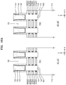
FIG. 1 is a layout diagram of an integrated circuit device according to example embodiments;
FIG. 2A illustrates cross-sectional views taken along line A1-A1′ and line A2-A2′ in FIG. 1, and FIG. 2B is a cross-sectional view taken along line B1-B1′ in FIG. 1;
FIG. 3A is an enlarged view of a region CX3A in FIG. 2B;
FIG. 3B is an enlarged view of a region CX3B in FIG. 3A;
FIG. 4 is a cross-sectional view of an integrated circuit device according to example embodiments;
FIG. 5 is a cross-sectional view of an integrated circuit device according to example embodiments;
FIG. 6 is a cross-sectional view of an integrated circuit device according to example embodiments;
FIGS. 7A through 25B are cross-sectional views for describing a method of manufacturing an integrated circuit device according to embodiments, where FIGS. 7A, 8A, 11A, 12 through 15, 16A, 17A, 18A, 19A, 20A, 21A, 22A, 23A, 24A, and 25A illustrate cross-sections taken along line A1-A1′ and line A2-A2′ in FIG. 1 according to the process sequence, and FIGS. 7B, 8B, 9, 10, 11B, 16B, 17B, 18B, 19B, 20B, 21B, 22B, 23B, 24B, and 25B illustrate cross-sections taken along line B1-B1′ in FIG. 1 according to the process sequence.
DETAILED DESCRIPTION OF THE EMBODIMENTS
Hereinafter, embodiments of the inventive concept will be described in detail with reference to the accompanying drawings. It will be understood that, although the terms first, second, third etc. may be used herein to describe various elements, components, regions, layers and/or sections, these elements, components, regions, layers and/or sections should not be limited by these terms. Unless the context indicates otherwise, these terms are only used to distinguish one element, component, region, layer or section from another element, component, region, layer or section, for example as a naming convention. Thus, a first element, component, region, layer or section discussed below in one section of the specification could be termed a second element, component, region, layer or section in another section of the specification or in the claims without departing from the teachings of the present invention. In addition, in certain cases, even if a term is not described using “first,” “second,” etc., in the specification, it may still be referred to as “first” or “second” in a claim in order to distinguish different claimed elements from each other.
FIG. 1 is a layout diagram of an integrated circuit device 100 according to example embodiments. FIG. 2A illustrates cross-sectional views taken along line A1-A1′ and line A2-A2′ in FIG. 1, FIG. 2B is a cross-sectional view taken along line B1-B1′ in FIG. 1, FIG. 3A is an enlarged view of a region CX3A in FIG. 2B, and FIG. 3B is an enlarged view of a region CX3B in FIG. 3A.
Referring to FIGS. 1 through 3B, a substrate 110 may be provided with a first fin-type active area FA1 and a second fin-type active area FA2. In an example embodiment, the first fin-type active area FA1 and the second fin-type active area FA2 may be formed by being epitaxially grown from the substrate 110 or by etching the substrate 110. The first fin-type active area FA1 and the second fin-type active area FA2 may constitute a first transistor TR1 and a second transistor TR2, respectively. In example embodiments, the first transistor TR1 may include an NMOS transistor, and the second transistor TR2 may include a PMOS transistor. In other embodiments, the first transistor TR1 may include an NMOS transistor having a first threshold voltage, and the second transistor TR2 may include a PMOS transistor having a second threshold voltage that is different from the first threshold voltage.
The substrate 110 may include a semiconductor material such as Si and Ge, or may include a compound semiconductor material such as SiGe, SiC, GaAs, InAs, and InP. In some embodiments, the substrate 110 may include at least one of a Group III-V material and a Group IV material. The Group III-V material may be a binary, ternary, or quaternary compound including at least one Group III element and at least one Group V element. The Group III-V material may be a compound containing at least one element of In, Ga, and Al as a Group III element and at least one element of As, P, and Sb as a Group V element. For example, the Group III-V material may be selected from InP, InzGa1-zAs (0≤z≤1), and AlzGa1-zAs (0≤z≤1). The binary compound may include, for example, InP, GaAs, InAs, InSb, or GaSb. The ternary compound may include any one of InGaP, InGaAs, AlInAs, InGaSb, GaAsSb, or GaAsP. The Group IV material may include Si or Ge. However, the Group III-V material and the Group IV material usable in the integrated circuit device 100 according to the inventive concept are not limited to those described above. The Group III-V material and the Group IV material such as Ge may be used as a channel material capable of forming a low-power, high-speed transistor. A semiconductor substrate including a Group III-V material having a higher electron mobility than that of a Si-based semiconductor substrate, for example, a GaAs-based semiconductor substrate, and a semiconductor substrate having a higher hole mobility than that of the Si-based semiconductor substrate, for example, a Ge-based semiconductor substrate may be used to form a high-performance CMOS. In some embodiments, when forming the NMOS transistor on the substrate 110, the substrate 110 may include any one of the above-exemplified Group III-V materials. In some other embodiments, when forming the PMOS transistor on the substrate 110, at least a portion of the substrate 110 may include Ge. In another example, the substrate 110 may have a semiconductor on insulator (SOI) structure. The substrate 110 may include a conductive region, for example, a well doped with impurities, or a structure doped with impurities.
Each of the first fin-type active area FA1 and the second fin-type active area FA2 may extend in a first direction (X direction) on the substrate 110, and protrude in the vertical direction (Z direction) from a top surface of the substrate 110. The second fin-type active area FA2 may be arranged spaced apart from the first fin-type active area FA1 in a second direction (Y direction) perpendicular to the first direction (X direction).
On the substrate 110, an element isolation trench 112T defining the first fin-type active area FA1 and the second fin-type active area FA2 may be formed, and a deep trench 114T defining an element region DR may be formed. An element isolation layer 112 may be in the element isolation trench 112T, and a deep trench insulation layer 114 may be in the deep trench 114T.
For example, the element isolation layer 112 may be between the first fin-type active area FA1 and the second fin-type active area FA2, and may include an element isolation liner 112L formed conformally on an inner wall of the element isolation trench 112T, and a gap fill isolation layer 1121 filling the inside of the element isolation trench 112T on the element isolation liner 112L. FIG. 2B illustrates an example in which a top surface of the element isolation layer 112 is at the same level as top surfaces of the first and second fin-type active areas FA1 and FA2. However, unlike this case, the top surface of the element isolation layer 112 may be positioned lower than the top surfaces of the first and second fin-type active areas FA1 and FA2, and only bottom portions on side walls of the first and second fin-type active areas FA1 and FA2 may be surrounded by the element isolation layer 112. The deep trench insulation layer 114 may include silicon oxide, silicon nitride, or a combination thereof.
A plurality of first semiconductor patterns NS1 may be arranged spaced apart from the top surface of the first fin-type active area FA1 in the vertical direction (Z direction) perpendicular to the top surface of the first fin-type active area FA1. The plurality of first semiconductor patterns NS1 may include the same material as the substrate 110. For example, the plurality of first semiconductor patterns NS1 may include a semiconductor material such as Si and Ge, or a compound semiconductor material such as SiGe, SiC, GaAs, InAs, and InP. Each of the plurality of first semiconductor patterns NS1 may include a channel region.
Each of the plurality of first semiconductor patterns NS1 may have a relatively large first width W11 in the second direction (Y direction) and a relatively small first thickness T11 in the vertical direction (Z direction), and for example, may have a nanosheet shape. In the example embodiments, each of the plurality of first semiconductor patterns NS1 may have the first width W11 ranging from about 5 nm to about 100 nm, and each of the plurality of first semiconductor patterns NS1 may have the first thickness T11 ranging from about 1 nm to about 10 nm, but the embodiments are not limited thereto.
As illustrated in FIG. 2B, the plurality of first semiconductor patterns NS1 may be arranged spaced apart from each other at an equal distance. However, the inventive concept is not limited thereto, and the plurality of first semiconductor patterns NS1 may be arranged spaced apart from each other at different distances. In addition, the number of first semiconductor patterns NS1 is not limited to those illustrated in FIGS. 2A and 2B.
A plurality of second semiconductor patterns NS2 may be arranged spaced apart from the top surface of the second fin-type active area FA2 in the vertical direction (Z direction) perpendicular to the top surface of the second fin-type active area FA2. The plurality of second semiconductor patterns NS2 may include the same material as the substrate 110, and each of the plurality of second semiconductor patterns NS2 may include a channel region.
Each of the plurality of second semiconductor patterns NS2 may have a relatively large second width W12 in the second direction (Y direction) and a relatively small second thickness T12 in the vertical direction (Z direction), and for example, may have a nanosheet shape. In the example embodiments, the second width W12 of each of the plurality of second semiconductor patterns NS2 may be the same as or different from the first width W11 of each of the plurality of first semiconductor patterns NS1. In addition, the second thickness T12 of each of the plurality of second semiconductor patterns NS2 may be equal to the first thickness T11 of each of the plurality of first semiconductor patterns NS1, but the present invention is not limited thereto.
A gate structure 120 may include a first gate structure 120A and a second gate structure 120B. The first gate structure 120A may extend in a second direction (Y direction) on the first fin-type active area FA1 and surround each of the plurality of first semiconductor patterns NS1. The first gate structure 120A may include a first main gate portion 120M1 covering a top surface of the uppermost first semiconductor pattern of the plurality of first semiconductor patterns NS1, and a plurality of first sub-gate portions 120S1 disposed between the uppermost first semiconductor pattern and the top surface of the first fin-type active area FA1. Each of the plurality of first sub-gate portions 120S1 may be disposed in a corresponding space of spaces between the first fin-type active area FA1 and the lowermost first semiconductor pattern of the plurality of first semiconductor patterns NS1 and between two adjacent first semiconductor patterns of the plurality of first semiconductor patterns NS1. The second gate structure 120B may extend in the second direction on the second fin-type active area FA2 and surround each of the plurality of second semiconductor patterns NS2. The second gate structure 120B may include a second main gate portion 120M2 covering a top surface of the uppermost second semiconductor pattern of the plurality of second semiconductor patterns NS2, and a plurality of second sub-gate portions 120S2 disposed between the uppermost second semiconductor pattern and the top surface of the second fin-type active area FA2. Each of the plurality of second sub-gate portions 120S2 may be disposed in a corresponding space of spaces between the second fin-type active area FA2 and the lowermost second semiconductor pattern of the plurality of second semiconductor patterns NS2 and between two adjacent second semiconductor patterns of the plurality of second semiconductor patterns NS2.
The first main gate portion 120M1 of the first gate structure 120A may include a first work function control layer 122, a buried conductive layer 126, and a gate insulation layer 128. The second main gate portion 120M2 of the second gate structure 120B may include a second work function control layer 124, the second buried conductive layer 126, and the gate insulation layer 128. Each of the plurality of first sub-gate portions 120S1 may include the first work function control layer 122 and the gate insulation layer 128. Each of the plurality of second sub-gate portions 120S2 may include the second work function control layer 124 and the gate insulation layer 128.
The gate insulation layer 128 may be on the top surfaces of the first and second fin-type active areas FA1 and FA2, and may extend onto the element isolation layer 112 and the deep trench insulation layer 114. The gate insulation layer 128 may surround each of the plurality of first semiconductor patterns NS1, and may surround each of the plurality of second semiconductor patterns NS2.
The first work function control layer 122 may surround each of the plurality of first semiconductor patterns NS1, and may extend over the element isolation layer 112 and the deep trench insulation layer 114. The first work function control layer 122 may fill an inner space of the plurality of first sub-gate portions 120S1 with the gate insulation layer 128. The second work function control layer 124 may surround each of the plurality of second semiconductor patterns NS2 and may fill the inner space of the plurality of second sub-gate portions 120S2 with the gate insulation layer 128. The buried conductive layer 126 may be on the first work function control layer 122 and the second work function control layer 124, and may fill the inner spaces of the first and second main gate portions 120M1 and 120M2.
As illustrated in FIG. 3B, the gate insulation layer 128 may have a stacked structure of an interface layer 128I and a high-k dielectric layer 128H. The interface layer 128I may remove or cure a defect of an interface between the top surfaces of the first and second fin-type active areas FA1 and FA2, and the high-k dielectric layer 128H, on surfaces of the plurality of first and second semiconductor patterns NS1 and NS2.
In an embodiment, the interface layer 128I may include a layer of a low-k dielectric material having a dielectric constant of about 9 or less, for example, a silicon oxide layer, a silicon oxynitride layer, a Ga oxide layer, a Ge oxide layer, or a combination thereof. In an embodiment, the interface layer 128I may include a silicate, a combination of silicate and a silicon oxide layer, or a combination of a silicate and a silicon oxynitride layer. In an embodiment, the interface layer 128I may be omitted.
The high-k dielectric layer 128H may include a material having a dielectric constant greater than the silicon oxide layer. For example, the high-k dielectric layer 128H may have a dielectric constant of about 10 to about 25. The high-k dielectric layer 128H may include hafnium oxide, hafnium oxynitride, hafnium silicon oxide, lanthanum oxide, lanthanum aluminum oxide, zirconium oxide, zirconium oxide, zirconium silicon oxide, tantalum oxide, titanium oxide, barium strontium titanium oxide, barium titanium oxide, strontium titanium oxide, yttrium oxide, aluminum oxide, lead scandium tantalum oxide, lead zinc niobate, or a combination thereof. However, the material constituting the high-k dielectric layer 128H is not limited thereto. The high-k dielectric layer 128H may be formed by an atomic layer deposition (ALD) process, a chemical vapor deposition (CVD) process, or a physical vapor deposition (PVD) process. The high-k dielectric layer 128H may have a thickness of about 10 Å to about 40 Å, but is not limited thereto.
In example embodiments, the first work function control layer 122 and the second work function control layer 124 may include Al, Cu, Ti, Ta, W, Mo, TaN, NiSi, CoSi, TiN, TiAlC, TiAlN, TaCN, TaC, TaSiN, or a combination thereof, but the embodiments are not limited thereto. The second work function control layer 124 may include a double-layer structure of a lower second work function control layer 124L and an upper second work function control layer 124U. The upper second work function control layer 124U may include the same material as the first work function control layer 122, and may be formed by using the same forming process as that of first work function control layer 122. In some examples, the first work function control layer 122 may include TiN, the lower second work function control layer 124L may include TiN, and the upper second work function control layer 124U may include TiN. In an example embodiment, the upper second work function control layer 124U and the first work function control layer 122 may be formed of the same material as each other, such as Al, Cu, Ti, Ta, W, Mo, TaN, NiSi, CoSi, TiN, TiAlC, TiAlN, TaCN, TaC, TaSiN, or a combination thereof. In an example embodiment, the lower second work function control layer 124L, the upper second work function control layer 124U and the first work function control layer 122 may be formed of the same material as each other, such as Al, Cu, Ti, Ta, W, Mo, TaN, NiSi, CoSi, TiN, TiAlC, TiAlN, TaCN, TaC, TaSiN, or a combination thereof.
In example embodiments, the buried conductive layer 126 may include A1, Cu, Ti, Ta, W, Mo, TaN, NiSi, CoSi, TiN, WN, TiAl, TiAlC, TiAlN, TaCN, TaC, TaSiN, or a combination thereof. However, the embodiments are not limited thereto.
A thickness T21 of the first work function control layer 122 in the vertical direction (Z direction) may be less than a thickness T22 of the second work function control layer 124 in the vertical direction (Z direction). Accordingly, the second transistor TR2 may have a second threshold voltage that is different from a first threshold voltage of the first transistor TR1. In addition, the thickness T21 of the first work function control layer 122 in the vertical direction (Z direction) may be equal to a thickness T23 of the upper second work function control layer 124U in the vertical direction (Z direction).
As illustrated in FIG. 3A, the first work function control layer 122 may include a step portion 122P protruding downward toward the element isolation layer 112 at a location where the first work function control layer 122 overlaps the element isolation layer 112. For example, the step portion 122P may be positioned on the element isolation layer 112. The gate insulation layer 128 may have a recess region 128R at a location where the gate insulation layer 128 vertically overlaps the step portion 122P of the first work function control layer 122, and the recess region 128R may be in contact with the step portion 122P of the first work function control layer 122. For example, the gate insulation layer 128 may include a portion recessed toward the element isolation layer 112 such that the recessed portion (i.e., the recess region 128R) of the gate insulation layer 128 may receive the step portion 122P. The gate insulation layer 128 may be in contact with the entire bottom surface of the step portion 122P, and accordingly, the first work function control layer 122 or the step portion 122P of the first work function control layer 122 may not be in contact with the element isolation layer 112. In FIG. 3A, the recess region 128R of the gate insulation layer 128 is illustrated as being formed to have a relatively flat bottom level. However, unlike this case, the recess region 128R of the gate insulation layer 128 may be formed to have a sloped bottom level.
The recess region 128R of the gate insulation layer 128 may be a region which is formed, after the plurality of second semiconductor patterns NS2 are covered by the second mask pattern 240P (refer to FIG. 24B), by using an etching process for removing a preliminary work function control layer 122X (refer to FIG. 24B) between the plurality of first semiconductor patterns NS1 (for example, the preliminary work function control layer 122X in the sub-gate space GSS), and by using a removal process of the second mask pattern 240P.
For example, the step portion 122P of the first work function control layer 122 may include a first step and a second step. The second step may be farther from the plurality of first semiconductor patterns NS1 than the first step. The second step may be spaced apart from the plurality of first semiconductor patterns NS1 in the second direction (Y direction) by a second spacing distance S21, and the second step of the step portion 122P of the first work function control layer 122 may be spaced apart from an end portion 124_E of the second work function control layer 124 (or, an edge portion of the second work function control layer 124 on the element isolation layer 112) in the second direction (Y direction) by a third spacing distance S22. In addition, the plurality of first semiconductor patterns NS1 and the plurality of second semiconductor patterns NS2 may be apart from each other by a first spacing distance S11 (refer to FIG. 1). The second spacing distance S21 may be less than the first spacing distance S11.
In the example embodiments, the first spacing distance S11 may be in a range of about 50% to about 200% of the first width W11 of the plurality of first semiconductor patterns NS1 (for example, ½ *W11≤S11≤2*W11) in the second direction (Y direction), and the second spacing distance S21 may be in a range of about 10% to about 100% of the first width W11 (for example, 1/10 *W11≤S21≤W11). The term of “about” may reflect amounts, sizes, orientations, or layouts that vary only in a small relative manner, and/or in a way that does not significantly alter the operation, functionality, or structure of certain elements. For example, a range from “about 0.1 to about 1” may encompass a range such as a 0%-5% deviation around 0.1 and a 0% to 5% deviation around 1, especially if such deviation maintains the same effect as the listed range.
For example, when the first spacing distance S11 is less than about 50% of the first width W11 of the plurality of first semiconductor patterns NS1, the preliminary work function control layer 122X (refer to FIG. 21B) formed between the first semiconductor patterns NS1 may not be completely removed. When the first spacing distance S11 is greater than about 200% of the first width W11 of the plurality of first semiconductor patterns NS1, it may be unnecessary to perform the two etching processes used for the first mask pattern 230P and the second mask pattern 240P, which are described later with reference to FIGS. 7A through 25B.
When the first spacing distance S11 is in the range of about 50% to about 200% of the first width W11 of the plurality of first semiconductor patterns NS1 in the second direction (Y direction), the step portion 122P may be formed in the first work function control layer 122 by performing the two etching processes used for the first mask pattern 230P and the second mask pattern 240P. As the edge of the second mask pattern 240P and the end portion 124_E of the second work function control layer 124 are spaced apart from each other, for example, by the spacing distance corresponding to the second spacing distance S21 in the range of about 10% to about 100% of the first width W11 of the plurality of first semiconductor patterns NS1, precision of a removal process of the preliminary work function control layer 122X may be increased.
Gate spacers 132 may be arranged on opposite sidewalls of the gate structure 120. The gate spacers 132 may include silicon nitride or silicon oxynitride. Although not illustrated, the gate spacers 132 may have a multi-layer structure including a plurality of material layers sequentially formed on opposite sidewalls of the gate structure 120.
A first recess RS1 may be formed in the first fin-type active area FA1. The first recess RS1 may be formed on both sides of a region of the first fin-type active area FA1 on which the plurality of first semiconductor patterns NS1 are disposed, and the first semiconductor layer 142 may fill the inside of the first recess RS1. The first semiconductor layer 142 may be connected to an end of each of the plurality of first semiconductor patterns NS1. The first semiconductor layer 142 may be grown from the first fin-type active area FA1 and the plurality of first semiconductor patterns NS1 by a selective epitaxial growth (SEG) process. In addition, a second recess RS2 may be formed in the second fin-type active area FA2. The second recess RS2 may be formed on opposite sides of a region of the second fin-type active area FA2 on which the plurality of second semiconductor patterns NS2 are disposed, and the second semiconductor layer 144 may fill the inside of the second recess RS2. The first semiconductor layer 142 and the second semiconductor layer 144 may include an epitaxially grown Si layer, an epitaxially grown SiC layer, an embedded SiGe structure including a plurality of epitaxially grown SiGe layers, etc.
Inner spacers 134 may be between the first semiconductor layer 142 and the gate structure 120, and between the second semiconductor layer 144 and the gate structure 120. Each of the inner spacers 134 may be between the first semiconductor layer 142 and the gate insulation layer 128 in a corresponding one of the plurality of first sub-gate portions 120S1, and between the second semiconductor layer 144 and the gate insulation layer 128 in a corresponding one of the plurality of second sub-gate portions 120S2. The inner spacers 134 may include silicon nitride or silicon oxynitride.
A gate insulation liner 152 and an inter-gate insulation layer 154 may be sequentially formed on opposite sidewalls of the gate spacer 132, on the first semiconductor layer 142, and on the second semiconductor layer 144. A first top insulation layer 162 and a second top insulation layer 164 may be sequentially arranged on the gate structure 120. A contact plug 166 may be in a contact hole 166H that exposes the top surfaces of the first semiconductor layer 142 and the second semiconductor layer 144 by passing through the first top insulation layer 162, and a metal silicide layer 168 may be further formed between the contact plug 166 and the first semiconductor layer 142, and between the contact plug 166 and the second semiconductor layer 144. The metal silicide layer 168 may include titanium silicide or cobalt silicide, but is not limited thereto.
A first wiring layer 172 may be connected to the contact plug 166, and the second wiring layer 174 may be connected to the gate structure 120. For example, the first wiring layer 172 may be in a first via hole 172H passing through the second top insulating layer 164, and a first barrier layer 172B may be further formed on the inner wall of the first via hole 172H. The second wiring layer 174 may be in a second via hole 174H passing through the first and second top insulation layers 162 and 164, and a second barrier layer 174B may be further formed on the inner wall of the second via hole 174H.
In general, to provide the first transistor TR1 and the second transistor TR2 constituted by the same gate layer structure (e.g., having the same types and arrangement of layers) with different threshold voltages from each other, after the preliminary work function control layer 122X (refer to FIG. 21B) is formed, a method of selectively removing only the preliminary work function control layer 122X from a first transistor forming region may be used. However, in an integrated circuit device including a plurality of semiconductor patterns of a nanosheet type, a level of difficulty may be relatively high in a process of removing selectively the preliminary work function control layer 122X in a space between each of the plurality of semiconductor patterns (for example, the sub-gate space GSS (refer to FIG. 21B)). Particularly, when the first width W11 of the plurality of first semiconductor patterns NS1 is relatively large and the first spacing distance S11 between the plurality of first semiconductor patterns NS1 is relatively small, the preliminary work function control layer 122X in the sub-gate space GSS may not be completely removed, and/or an unwanted etching may occur in the preliminary work function control layer 122X in a second transistor forming region. In this case, a precise control of the threshold voltage of the integrated circuit device 100 may be difficult.
However, in the method of manufacturing the integrated circuit device 100 according to the above-described example embodiments, a first mask pattern 230P (refer to FIG. 21B) may be used to remove first only the portion of the preliminary work function control layer 122X on the top surface and the side wall of the plurality of first semiconductor patterns NS1, and thereafter, a second mask pattern 240P (refer to FIG. 23B) may be used as an etching mask to remove the portion of the preliminary work function control layer 122X filling a space between each of the plurality of first semiconductor patterns NS1 (that is, the portion of the preliminary work function control layer 122X in the sub-gate space GSS). Since the second mask pattern 240P completely covers the portion of the preliminary work function control layer 122X in the second transistor forming region, unwanted etching of the preliminary work function control layer 122X in the second transistor forming region may be prevented, while it is possible to completely remove the portion of the preliminary work function control layer 122X in the sub-gate space GSS in the first transistor forming region. Thus, a precise control of the threshold voltage of the integrated circuit device 100 may be possible.
FIG. 4 is a cross-sectional view of an integrated circuit device 100A according to example embodiments. FIG. 4 is a cross-sectional view of a portion corresponding to a region CX3B in FIG. 3A.
Referring to FIG. 4, the gate insulation layer 128A may include an interface layer 128IA and a high-k dielectric layer 128HA, and the stepped portion 122PA of the first work function control layer 122 may pass through the high-k dielectric layer 128HA to be in contact with the interface layer 128IA. The term “contact,” or “in contact with,” as used herein, refers to a direction connection (i.e., touching) unless the context indicates otherwise. A protrusion 128IA_T of the interface layer 128IA may be formed at a position where the high-k dielectric layer 128HA is removed. The protrusion portion 128IA_T of the interface layer 128IA may be in contact with the stepped portion 122PA of the first work function control layer 122, and the high-k dielectric layer 128HA may surround the stepped portion 122PA of the first work function control layer 122. A level of a top surface of the protrusion portion 128IA_T may be higher than a level of a top surface of the interface layer 128IA on the first fin-type active area FA1 (refer to FIG. 2B).
In example embodiments, in a wet etching process using the second mask pattern 240P (refer to FIG. 24B) and/or in a removing process of the second mask pattern 240P, a portion of the gate insulation layer 128A that is on the element isolation layer 112 and exposed to an etching atmosphere, that is, the portion of the high-k dielectric layer 128HA, may be removed together to form a recess region 128RA in the gate insulation layer 128A. However, in the wet etching process, additional oxidation of the interface layer 128IA may occur as the portion of the high-k dielectric layer 128HA is removed and the interface layer 128IA under the high-k dielectric layer 128HA is exposed, and accordingly, the protrusion portion 128IA_T may be formed on an exposed portion of the interface layer 128IA.
FIG. 5 is a cross-sectional view of an integrated circuit device 100B according to an embodiment. FIG. 5 is a cross-sectional view of a portion corresponding to the region CX3A in FIG. 2B.
Referring to FIG. 5, a first work function control layer 122B may include a lower first work function control layer 122LB and an upper first work function control layer 122UB. In some embodiments, the lower first work function control layer 122LB may include TaN, and the upper first work function control layer 122UB may include TiN.
A second work function control layer 124B may include a lower second work function control layer 124LB, an intermediate second work function control layer 124MB, and an upper second work function control layer 124UB. In some embodiments, the lower second work function control layer 124LB may include TaN, the intermediate second work function control layer 124MB may include TiN, and the upper second work function control layer 124UB may include TiN.
For example, after a preliminary work function control layer (not shown) including the lower second work function control layer 124LB and the intermediate second work function control layer 124MB is first formed, the intermediate second work function control layer 124MB may be selectively removed from the first fin-type active area FA1. The removal process may be a wet etching process using etching selectivity of the intermediate second work function control layer 124MB with reference to the lower second work function control layer 124LB, and in this case, a portion of the lower second work function control layer 124LB may be removed together with the intermediate second work function control layer 124MB, and a recess region 122BR may be formed in the lower second work function control layer 124LB. Thereafter, the upper second work function control layer 124UB may be formed on the lower second work function control layer 124LB.
Material layers formed in the same process for the lower second work function control layer 124LB and the upper second work function control layer 124UB may remain in the first fin-type active area FA1, and each of the material layers may be referred to as the lower first work function control layer 122LB and the upper first work function control layer 122UB. Accordingly, a thickness T23B of the upper second work function control layer 124UB may be equal to a thickness T21B of the upper first work function control layer 122UB. In addition, the upper first work function control layer 122UB may include a step portion 122PB at a portion where the upper first work function control layer 122UB is in contact with the recess region 122BR.
FIG. 6 is a cross-sectional view of an integrated circuit device 100C according to an embodiment. FIG. 6 is a cross-sectional view of a portion corresponding to the region CX3A in FIG. 2B.
Referring to FIG. 6, a buried insulation layer 118A may be on a substrate 110A, and a first active area AC1 and a second active area AC2 may be on the buried insulation layer 118A. An element isolation layer 118B may be between the first active area AC1 and the second active area AC2. The first active area AC1 and the second active area AC2 may include the same material as the substrate 110A. The present invention, however, is not limited thereto. In an example embodiment, the first active area AC1 and the second active area AC2 may include a different material from the substrate 110A. The first active area AC1 and the second active area AC2 may be a part of an epitaxial semiconductor layer on the substrate 110A and the buried insulation layer 118A, and the substrate 110A may be a substrate of an insulator (SOI) type.
FIGS. 7A through 25B are cross-sectional views illustrating a method of manufacturing the integrated circuit device 100 according to example embodiments. FIGS. 7A, 8A, 11A, 12 through 15, 16A, 17A, 18A, 19A, 20A, 21A, 22A, 23A, 24A, and 25A illustrate cross-sections taken along line A1-A1′ and line A2-A2′ in FIG. 1 according to the process sequence, and FIGS. 7B, 8B, 9, 10, 11B, 16B, 17B, 18B, 19B, 20B, 21B, 22B, 23B, 24B, and 25B illustrate cross-sections taken along line B1-B1′ in FIG. 1 according to the process sequence.
Referring to FIGS. 7A and 7B, a sacrifice layer structure 210S may be formed by alternately and sequentially forming a sacrificial layer 210 and a channel semiconductor layer PNS on a top surface 110M of a substrate 110. The sacrificial layer 210 and the channel semiconductor layer PNS may be formed by an epitaxy process.
In example embodiments, the sacrificial layer 210 and the channel semiconductor layer PNS may include materials having different etch selectivity from each other. For example, each of the sacrificial layer 210 and the channel semiconductor layer PNS may include a single crystal layer of a Group IV semiconductor, a single crystal layer of a Group IV-IV compound semiconductor or a single crystal layer of a Group III-V compound semiconductor, or may include a different material from each other. In an example, the sacrificial layer 210 may include SiGe, and the channel semiconductor layer PNS may include mono-crystalline silicon.
In example embodiments, the epitaxy process may include a chemical vapor deposition (CVD) process such as a vapor-phase epitaxy (VPE) process and an ultra-high vacuum chemical vapor deposition (UHV-CVD) process, a molecular beam epitaxy process, or a combination thereof. In the epitaxy process, a liquid or gaseous precursor may be used as a precursor required for forming the sacrificial layer 210 and the channel semiconductor layer PNS.
Referring to FIGS. 8A and 8B, after a lower layer 222U and a hardmask pattern 222M extending in a first direction (X direction) by a certain length are formed on the channel semiconductor layer PNS, a sacrifice pattern structure 210SP and an element isolation trench 112T may be formed by etching the sacrificial layer 210, the channel semiconductor layer PNS, and the substrate 110 by using the lower layer 222U and the hardmask pattern 222M as etching masks. The sacrifice pattern structure 210SP may include a sacrificial layer pattern 210P and a channel semiconductor layer pattern PNSP formed by etching the sacrificial layer 210 and the channel semiconductor layer PNS.
Referring to FIG. 9, an element isolation layer 112 may be formed to fill the element isolation trench 112T. In an example embodiment, an element isolation liner 112L may be formed conformally in the element isolation trench 112T, a gap fill isolation layer 1121 may be formed on the element isolation liner 112L to fill the element isolation trench 112T, and a top portion of the gap fill isolation layer 1121 may be planarized, and then the element isolation layer 112 filling the element isolation trench 112T may be formed.
Referring to FIG. 10, a deep trench 114T defining the element region DR may be formed by etching portions of the element isolation layer 112 and the substrate 110, and a deep trench insulation layer 114 may be formed in the deep trench 114T.
Thereafter, the lower layer 222U and the hardmask pattern 222M remaining on the sacrifice pattern structure 210SP may be removed, and a recess process may be performed for removing top portions of the element isolation layer 112 and the deep trench insulation layer 114 by a certain thickness.
Referring to FIGS. 11A and 11B, a dummy gate structure DG may be formed on the sacrifice pattern structure 210SP (refer to FIG. 9) and the element isolation layer 112. The dummy gate structure DG may include a dummy gate insulation layer DGI, a dummy gate line DGL, a dummy gate capping layer DGC, and a dummy gate spacer DGS.
For example, the dummy gate line DGL may include polysilicon, and the dummy gate capping layer DGC may include a silicon nitride layer. The dummy gate insulation layer DGI may include a material having etch selectivity with respect to the dummy gate line DGL, and may include at least one layer of, for example, thermal oxide, silicon oxide, and silicon nitride. The dummy gate spacer DGS may include silicon oxide, silicon oxynitride, or silicon nitride, but the embodiment is not limited thereto.
Referring to FIG. 12, a first recess RS1 and a second recess RS2 may be formed by etching portions of the sacrifice pattern structure 210SP and the substrate 110 using the dummy gate structure DG as an etching mask. The sacrificial layer pattern 210P and the channel semiconductor layer pattern PNSP may be further patterned to form a sacrificial pattern 210PP and a channel semiconductor pattern PNSPP. Side walls of the sacrificial pattern 210PP and the channel semiconductor pattern PNSPP may be exposed on the inner walls of the first and second recesses RS1 and RS2.
Referring to FIG. 13, a recess region 210H may be formed between two adjacent channel semiconductor patterns PNSPP by removing a portion of the sacrificial pattern 210PP exposed inside the first recess RS1 and the second recess RS2 by using an isotropic etching process. In an example embodiment, the recess region 210H may be formed by recessing the inner walls of the first and second recesses RS1 and RS2 in the first direction using an isotropic etching process. For example, the recess region 210H may be formed between two adjacent channel semiconductor patterns PNSPP stacked vertically on each other by removing a portion of the sacrificial pattern 210PP interposed therebetween. The portion of the sacrificial pattern 210PP may be exposed inside the first recess RS1 and the second recess RS2, and may be etched by performing the isotropic etching process using the channel semiconductor pattern PNSPP as an etching mask. In example embodiments, the recess region 210H may be formed by performing a wet etching process, as an example embodiment of the isotropic etching process, with etching selectivity of the sacrificial pattern 210PP with respect to the channel semiconductor pattern PNSPP. In the wet etching process, for example, the sacrificial pattern 210PP including SiGe may be etched faster than the channel semiconductor pattern PNSPP including, for example, Si, and accordingly, the recess region 210H may be formed.
Referring to FIG. 14, an inner spacer 134 filling the recess region 210H exposed to the inner walls of the first and second recesses RS1 and RS2 may be formed. The inner spacer 134 may be formed by forming an insulation layer (not shown) on the dummy gate structure DG and on the inner walls of the first and second recesses RS1 and RS2 with the recess region 210H to fill the inside of the recess region 210H, and then removing the insulation layer (not shown) on outer walls of the dummy gate structure DG and the inner walls of the first and second recesses RS1 and RS2. In an example embodiment, the removing of the insulation layer may be performed using a directional etching process such as a reactive ion etching (RIE) process.
Referring to FIG. 15, a first semiconductor layer 142 and a second semiconductor layer 144 may be formed inside the first recess RS1 and the second recess RS2, respectively. In an example embodiment, the first semiconductor layer 142 and the second semiconductor layer 144 may be formed by epitaxially growing a semiconductor material from surfaces of the substrate 110 and the channel semiconductor pattern PNSPP exposed to the inner wall of the first recess RS1 and the second recess RS2, respectively.
In FIGS. 12 through 15, a method is illustrated in which the first recess RS1 and the second recess RS2 may be simultaneously formed in the first fin-type active area FA1 and the second fin-type active area FA2, respectively, and then the first semiconductor layer 142 and the second semiconductor layer 144 may be simultaneously formed. However, when, for example, the first fin-type active area FA1 is an area for forming an NMOS transistor, and the second fin-type active area FA2 is an area for forming a PMOS transistor, after a protection layer (not shown) is formed on the second fin-type active area FA2, the first recess R1 and the first semiconductor layer 142 may be formed first, and after a protection layer (not shown) may be formed on the first fin-type active area FA1, and then the second recess RS2 and the second semiconductor layer 144 may be formed. In this case, a material included in the first semiconductor layer 142 and a material that included in the second semiconductor layer 144 may be different from each other. For example, p-type impurities may be doped in the first semiconductor layer 142 and n-type impurities may be doped in the second semiconductor layer 144.
Thereafter, a gate insulation liner 152 and an inter-gate insulation layer 154 may be formed on the sidewall of the dummy gate structure DG, and on the first semiconductor layer 142 and the second semiconductor layer 144. In an example embodiment, a preliminary gate insulation liner and a preliminary inter-gate insulation layer may be formed in the listed order on the sidewall of the dummy gate structure DG, and on the first semiconductor layer 142 and the second semiconductor layer 144. The preliminary gate insulation liner, and the preliminary inter-gate insulation layer on an upper surface of the gate capping layer DGC may be removed using a planarization process. In an example embodiment, the dummy gate capping layer DGC (refer to FIG. 14) of the dummy gate structure DG may also be removed in the planarization process, and then a top surface of the gate line DGL may be exposed. An upper portion of the dummy gate spacer DGS disposed on sidewalls of the dummy gate capping layer DGC may also be removed in the planarization process.
Referring to FIGS. 16A and 16B, the dummy gate line DGL and the dummy gate insulation layer DGI, which are exposed in the planarization process for forming the inter-gate insulation layer 154, may be removed, and then the gate space GS may be formed. The dummy gate spacer DGS exposed by the gate space GS may be referred to as a gate spacer 132.
Referring to FIGS. 17A and 17B, by removing the plurality of sacrificial layers 210 remaining on the first and second fin-type active areas FA1 and FA2 exposed through the gate space GS, upper and lower surfaces of the channel semiconductor pattern PNSPP and top surfaces the first and second fin-type active areas FA1 and FA2 may be exposed through the gate space GS. The channel semiconductor pattern PNSPP remaining in the first fin-type active area FA1 may be referred to as the plurality of first semiconductor patterns NS1, the channel semiconductor pattern PNSPP remaining in the second fin-type active area FA2 may be referred to as the plurality of second semiconductor patterns NS2, and a sub-gate space GSS may be formed between two first semiconductor patterns adjacent vertically to each other, between two second semiconductor patterns adjacent vertically to each other, between the top surface of the first fin-type active area FA1 and the lowermost first semiconductor pattern of the plurality of first semiconductor patterns NS1 and/or between the top surface of the second fin-type active area FA2 and the lowermost second semiconductor pattern of the plurality of second semiconductor patterns NS2.
The removal process of the sacrificial pattern 210PP may be a wet etching process using etching selectivity of the sacrificial pattern 210PP with respect to the channel semiconductor pattern PNSPP. During the wet etching process, the sacrificial pattern 210PP may be recessed between two first semiconductor patterns adjacent vertically to each other and/or two second semiconductor patterns adjacent vertically to each other to form an inner spacer 134. In this case, the sacrificial pattern 210PP and the inner spacer 134 may be formed of the same material. The inner spacer 134 that is not be removed in the wet etching process may be exposed on the inner wall of the sub-gate space GSS. In an example embodiment, the sacrificial pattern 210PP of FIGS. 16A and 16B may be partially removed through the gate space GS using the wet etching process to form the sub-gate space GSS, and the reaming portion of the sacrificial pattern 210PP may be referred to as the inner spacer 134. The sub-gate space GSS may be connected to the gate space GS. The sub-gate space GSS may be a region defined by an upper surface of a first semiconductor pattern, a lower surface of another first semiconductor pattern adjacent thereto, and a sidewall of the inner spacer 134. The lowermost gate space may be a region defined by the top surface of the first fin-type active area FA1, a lower surface of the lowermost first semiconductor pattern and a sidewall of the lowermost inner spacer on the first fin-type active area FA1 and/or a region defined by the top surface of the second fin-type active area FA2, a lower surface of the lowermost second semiconductor pattern and a sidewall of the lowermost inner spacer on the second fin-type active area FA2.
Referring to FIGS. 18A and 18B, a gate insulation layer 128 may be conformally formed on the surfaces exposed to the gate space GS and the sub-gate space GSS. Thereafter, a preliminary work function control layer 122X may be formed conformally on the gate insulation layer 128. The gate insulation layer 128 and the preliminary work function control layer 122X may also be formed on the element isolation layer 112 and the deep trench insulation layer 114.
In example embodiments, the preliminary work function control layer 122X may fill both the sub-gate space GSS disposed between two adjacent first semiconductor patterns of the plurality of first semiconductor patterns NS1 and the sub-gate space GSS disposed between two adjacent second semiconductor patterns of the plurality of second semiconductor patterns NS2. The present invention is not limited thereto. In an example embodiment, the preliminary work function control layer 122X may be formed with a thickness in a manner that the preliminary work function control layer 122X does not fill a portion of the inside of the sub-gate space GSS between two adjacent first semiconductor patterns of the plurality of first semiconductor patterns NS1, and a portion of the inside of the sub-gate space GSS between two adjacent second semiconductor patterns of the plurality of second semiconductor patterns NS2. In an example embodiment, the preliminary work function control layer 122X may be formed so that the sub-gate space GSS is completely filled, the sub-gate space GSS is partially filled or the sub-gate space GSS is not filled, depending on the thickness of the preliminary work function control layer 122X.
The preliminary work function control layer 122X may include Al, Cu, Ti, Ta, W, Mo, TaN, NiSi, CoSi, TiN, WN, TiAl, TiAlC, TiAlN, TaCN, TaC, TaSiN, or a combination thereof. In some examples, the preliminary work function control layer 122X may be formed as a single layer formed of TiN. In another example, the preliminary work function control layer 122X may be formed in a bi-layer structure that includes a lower layer formed of TaN and an upper layer formed of TiN.
Referring to FIGS. 19A and 19B, a mask material layer 230 filling the gate space GS may be formed on the preliminary work function control layer 122X. Thereafter, a lower layer 232U and a hardmask pattern 232M may be formed on the mask material layer 230 overlapping the second fin-type active area FA2.
In example embodiments, the mask material layer 230 may include a carbon-based insulation material. For example, the mask material layer 230 may include a material having a relatively high carbon content ratio. For example, the mask material layer 230 may include a material such as SiC:H, SiCN, SiCN:H, silicon oxycarbide (SiOCN), spin on hardmask (SOH), Si based anti-reflective coating (ARC), spin on glass (SOG), advanced planarization layer (APL), and organic dielectric layer (ODL), but the material is not limited thereto.
Referring to FIGS. 20A and 20B, by etching the mask material layer 230 by using the lower layer 232U and the hardmask pattern 232M as etching masks, a first mask pattern 230P covering a structure on the top portion of the second fin-type active area FA2 may be formed. Accordingly, the gate space GS may be formed again, and a portion of the preliminary work function control layer 122X surrounding each of the plurality of first semiconductor patterns NS1 on the first fin-type active area FA1 may be exposed by the gate space GS.
Referring to FIGS. 21A and 21B, a portion of the preliminary work function control layer 122X disposed on the first fin-type active area FA1, a portion of the preliminary work function control layer 122X disposed on the element isolation layer 112, and a portion of the preliminary work function control layer 122X disposed on the deep trench insulation layer 114 may be removed by using the first mask pattern 230P as an etching mask.
In example embodiments, the removal process of the preliminary work function control layer 122X by using the first mask pattern 230P may be a wet etching process. The wet etching process may be performed during a time period (or, a first etching period) in which the preliminary work function control layer 122X on the sidewall of the gate space GS is removed so that the gate space GS is formed again. As illustrated in FIG. 21B, a portion of the preliminary work function control layer 122X on the top surface of the uppermost first semiconductor pattern, a portion of the preliminary work function control layer 122X on the sidewall of each of the plurality of first semiconductor patterns NS1, the element isolation layer 112, and a portion of the preliminary work function control layer 122X on the deep trench insulation layer 114 may be removed, and the gate insulation layer 128 may be exposed to the inner wall of the gate space GS. On the other hand, in the wet etching process using the first mask pattern 230P as an etching mask, a portion of the preliminary work function control layer 122X between two first semiconductor patterns adjacent vertically to each other may remain without being etched. Accordingly, after performing the wet etching process using the first mask pattern 230P, the preliminary work function control layer 122X may remain as filling in the sub-gate space GSS.
As illustrated in FIG. 21B, in the wet etching process using the first mask pattern 230P as an etching mask, a portion of the preliminary work function control layer 122X between a side wall 230PS of the first mask pattern 230P and the gate insulation layer 128 may be also removed, and an undercut region 122XU defined by the preliminary work function control layer 122X may be formed under the side wall of the first mask pattern 230P.
Referring to FIGS. 22A and 22B, the first mask pattern 230P (refer to FIG. 21B) may be removed.
Referring to FIGS. 23A and 23B, a mask material layer (not shown) filling the gate space GS may be formed on the preliminary work function control layer 122X and the gate insulation layer 128, and the second mask pattern 240P covering the structure above the second fin-type active area FA2 may be formed by patterning the mask material layer (not shown). The second mask pattern 240P may be formed by using the same material and manufacturing method as the first mask pattern 230P.
In this case, the second mask pattern 240P may be arranged to completely cover an end portion of the preliminary work function control layer 122X extending from the preliminary work function control layer 122X formed in the second fin-type active area FA2. For example, the sidewall 240PS of the second mask pattern 240P may be apart from the end portion of the preliminary work function control layer 122X by a distance corresponding to the third distance S22, and accordingly, the preliminary work function control layer 122X may not be exposed in the gate space GS.
Referring to FIGS. 24A and 24B, portions of the preliminary work function control layers 122X between two first semiconductor patterns adjacent vertically to each other may be removed by using the second mask pattern 240P as an etching mask.
The removing process of the preliminary work function control layer 122X by using the second mask pattern 240P may be a wet etching process. The wet etching process may be performed for a relatively long time until the portion of the preliminary work function control layer 122X inside the sub-gate space GSS is completely removed. For example, in the wet etching process, an etchant or etching gas may penetrate into the inside of the sub-gate space GSS in a second direction (Y direction) to remove the preliminary work function control layer 122X, and then, each of the plurality of first semiconductor patterns NS1 may have the relatively large first width W11 in the second direction (Y direction). Accordingly, the wet etching process may be performed during a second etching period longer than the first etching period, and the second etching period may be relatively long enough, for example, to remove about 50% of the first width W11.
In the wet etching process using the second mask pattern 240P, since the end portion of the preliminary work function control layer 122X extending from the preliminary work function control layer 122X formed on the second fin-type active area FA2 is completely covered by the second mask pattern 240P, the portion of the preliminary work function control layer 122X on the second fin-type active area FA2 may not be exposed.
After all portions of the preliminary work function control layers 122X between two first semiconductor patterns adjacent vertically to each other are removed, the second mask pattern 240P may be removed.
In the wet etching process using the second mask pattern 240P and/or in the process of removing the second mask pattern 240P, a portion of the gate insulation layer 128 which is on the element isolation layer 112 and exposed to the etching atmosphere may be removed together with the second mask pattern 240P so that a recess region 128R may be formed in the gate insulating layer 128. Although the recess region 128R is illustrated as being formed to have a relatively flat bottom level under the sidewalls of the second mask pattern 240P, a shape of the recess region 128R may be different from the shape thereof illustrated in FIG. 24B according to wet etch process conditions and second mask pattern 240P removal process conditions, etc.
Referring to FIGS. 25A and 25B, a first work function control layer 122 may be formed on the gate insulation layer 128 on the first fin-type active area FA1, and an upper second work function control layer 124U may be formed on the preliminary work function control layer 122X on the second fin-type active area FA2. The portion of the preliminary work function control layer 122X on the second fin-type active area FA2 may be referred to as a lower second work function control layer 124L. The first work function control layer 122 may include a step portion 122P that is formed to be in contact with the recess region 128R of the gate insulation layer 128.
Referring again to FIGS. 2A and 2B, the buried conductive layer 126 filling the gate space GS may be formed on the first and second work function control layers 122 and 124, and the gate structure 120 may be formed by planarizing the top portion of the buried conductive layer 126 until the top surface of the inter-gate insulation layer 154 is exposed.
Thereafter, the first top insulation layer 162 may be formed, the contact hole 166H penetrating through the first top insulation layer 162 may be formed, and then the contact plug 166 may be formed by filling the contact hole 166H with a conductive material. Thereafter, the second top insulation layer 164 may be formed, and by performing a forming process of the via holes (172H and 174H) and a filling process of the conductive layer, the first wiring layer 172 and the second wiring layer 174 may be further formed.
According to the above-described method of manufacturing the integrated circuit device 100, only the portions of the preliminary work function control layers 122X on the top surface and on the side wall of each of the plurality of first semiconductor patterns NS1 are first removed by using the first mask pattern 230P as an etching mask, and then, the portion of the preliminary work function control layer 122X filling the space between two first semiconductor patterns adjacent vertically to each other (that is, the portion of the preliminary work function control layer 122X in the sub-gate space GSS) may be removed by using the second mask pattern 240P as an etching mask. Since the second mask pattern 240P completely covers the portion of the preliminary work function control layer 122X in the second transistor forming region, unwanted etching of the preliminary work function control layer 122X in the second transistor forming region may be prevented, while it is possible to completely remove the portion of the preliminary work function control layer 122X in the sub-gate space GSS in the first transistor forming region. Therefore, a precise control of the threshold voltage of the integrated circuit device 100 may be possible.
While the inventive concept has been particularly shown and described with reference to embodiments thereof, it will be understood that various changes in form and details may be made therein without departing from the spirit and scope of the following claims.

Claims (18)

What is claimed is:
1. An integrated circuit device comprising:
a first fin-type active area protruding from a surface of a substrate and extending in a first direction;
a second fin-type active area protruding from the surface of the substrate, the second fin-type active area being spaced apart from the first fin-type active area in a second direction perpendicular to the first direction;
an element isolation layer between the first fin-type active area and the second fin-type active area on the substrate;
a plurality of first semiconductor patterns on a top surface of the first fin-type active area, each of the plurality of first semiconductor patterns having a channel area;
a plurality of second semiconductor patterns on a top surface of the second fin-type active area, each of the plurality of second semiconductor patterns having a channel area;
a first gate structure extending on the first fin-type active area in the second direction, the first gate structure including a first work function control layer surrounding each of the plurality of first semiconductor patterns and including a step portion on the element isolation layer;
a second gate structure extending on the second fin-type active area in the second direction, the second gate structure including a second work function control layer surrounding each of the plurality of second semiconductor patterns; and
a gate insulation layer disposed on the first fin-type active area, the second fin-type active area, and the element isolation layer,
wherein the gate insulation layer includes a recess region on the element isolation layer, and
wherein the recess region of the gate insulation layer is in contact with the step portion of the first work function control layer.
2. The integrated circuit device of claim 1, wherein
the first work function control layer has a first thickness in a third direction perpendicular to the surface of the substrate,
the second work function control layer has a second thickness that is greater than the first thickness in the third direction, and
the step portion is disposed on the element isolation layer at a first distance in the second direction from an end portion of the second work function control layer.
3. The integrated circuit device of claim 1, further comprising:
a conductive layer disposed on the substrate and extending in the second direction,
wherein the first gate structure further includes:
a first portion of the conductive layer on the first work function control layer; and
a first portion of the gate insulation layer between the first fin-type active area and the first work function control layer, and between the first work function control layer and each of the plurality of first semiconductor patterns,
wherein the second gate structure further includes:
a second portion of the conductive layer on the second work function control layer; and
a second portion of the gate insulation layer, the second portion of the gate insulation layer being disposed between the second fin-type active area and the second work function control layer, and between the second work function control layer and each of the plurality of second semiconductor patterns.
4. The integrated circuit device of claim 3, wherein
the gate insulation layer is between a top surface of the element isolation layer and the step portion of the first work function control layer to separate the element isolation layer from the first work function control layer.
5. The integrated circuit device of claim 3, wherein
the gate insulation layer has a laminated structure in which an interface layer and a high-k dielectric layer are sequentially arranged on the element isolation layer, and
the step portion of the first work function control layer passes through the high-k dielectric layer to be in contact with the interface layer.
6. The integrated circuit device of claim 1,
wherein the gate insulation layer has a laminated structure in which an interface layer and a high-k dielectric layer are sequentially arranged on the element isolation layer, and
wherein the recess region is formed in a portion of the high-k dielectric layer, and the recess region of the high-k dielectric layer is interposed between the step portion of the first work function control layer and the interface layer.
7. The integrated circuit device of claim 1, wherein
a bottom surface of the step portion of the first work function control layer is positioned lower than a bottom surface of a portion of the second work function control layer disposed on the element isolation layer.
8. The integrated circuit device of claim 1, wherein
each of the plurality of first semiconductor patterns has a first width in the second direction,
the plurality of first semiconductor patterns and the plurality of second semiconductor patterns are spaced apart from each other by a first distance in the second direction,
the plurality of first semiconductor patterns and the step portion of the first work function control layer are spaced apart from each other by a second distance in the second direction, and
the second distance is less than the first distance.
9. The integrated circuit device of claim 8, wherein
the first distance is in a range of about 50% to about 200% of the first width.
10. The integrated circuit device of claim 1, wherein
the first work function control layer and the second work function control layer are formed of the same material including TiN, and
a thickness of the second work function control layer is greater than that of the first work function control layer.
11. The integrated circuit device of claim 1, wherein
the first work function control layer has a multi-layer structure of a lower first work function control layer including TaN and an upper first work function control layer including TiN, and
the second work function control layer has a triple-layer structure of a lower second work function control layer including TaN, an intermediate second work function control layer including TiN, and an upper second work function control layer including TiN.
12. The integrated circuit device of claim 11, wherein
a thickness of the upper second work function control layer is identical with that of the upper first work function control layer, and
a thickness of the lower second work function control layer is identical with that of the lower first work function control layer.
13. An integrated circuit device comprising:
a first fin-type active area protruding from a surface of a substrate and extending in a first direction;
a second fin-type active area protruding from the surface of the substrate, the second fin-type active area being spaced apart from the first fin-type active area in a second direction perpendicular to the first direction;
an element isolation layer between the first fin-type active area and the second fin-type active area on the substrate;
a plurality of first semiconductor patterns being spaced apart from a top surface of the first fin-type active area, each of the plurality of first semiconductor patterns having a channel area;
a plurality of second semiconductor patterns being spaced apart from a top surface of the second fin-type active area, each of the plurality of second semiconductor patterns having a channel area;
a first work function control layer including a first portion surrounding each first semiconductor pattern of the plurality of first semiconductor patterns, a second portion on the element isolation layer, and a connecting portion connecting the first portion and the second portion to each other, the second portion of the first work function control layer including a step portion on the element isolation layer and having a first thickness;
a second work function control layer including a third portion surrounding each second semiconductor pattern of the plurality of second semiconductor patterns and a fourth portion extending from the third portion onto the element isolation layer, the fourth portion of the second work function control layer having a second thickness that is greater than the first thickness; and
a gate insulation layer between the first fin-type active area and the first work function control layer, between the first work function control layer and each of the plurality of first semiconductor patterns and, between the second fin-type active area and the second work function control layer, and between the second work function control layer and each of the plurality of second semiconductor patterns,
wherein the gate insulation layer includes a recess region at a portion where the gate insulation layer is in contact with the step portion.
14. The integrated circuit device of claim 13, wherein,
the step portion is positioned at a predetermined distance from an end portion of the fourth portion of the second work function control layer.
15. The integrated circuit device of claim 13,
wherein the second work function control layer has a double-layer structure comprising a lower first work function control layer and an upper first work function control layer which are arranged sequentially on the second fin-type active area and each of the plurality of second semiconductor patterns,
wherein the upper first work function control layer is connected to the first work function control layer, and
wherein a location where the upper first work function control layer and the first work function control layer are connected to each other is on a portion of the element isolation layer between the recess region of the element isolation layer and the second fin-type active area.
16. An integrated circuit device comprising:
a buried insulation layer on a substrate;
a first active area, a second active area and an element isolation layer on the buried insulation layer, wherein the first active area and the second active area are arranged spaced apart from each other by the element isolation layer;
a plurality of first semiconductor patterns on the first active area, the plurality of first semiconductor patterns being spaced apart from a top surface of the first active area and each of the plurality of first semiconductor patterns having a channel area;
a plurality of second semiconductor patterns on the second active area, the plurality of second semiconductor patterns being apart from a top surface of the second active area and each of the plurality of second semiconductor patterns having a channel area;
a first work function control layer including a first portion surrounding each of the plurality of first semiconductor patterns and a second portion extending from the first portion onto the element isolation layer, the second portion of the first work function control layer including a first step portion which is on the element isolation layer and has a first thickness, and a second step portion; and
a second work function control layer including a third portion surrounding each of the plurality of second semiconductor patterns, a fourth portion extending from the third portion onto the element isolation layer, the fourth portion of the second work function control layer having a second thickness being greater than the first thickness,
wherein the first step portion of the first work function control layer is disposed between the second step portion of the first work function control layer and the first active area, and
wherein the second step portion of the first work function control layer is connected to the second work function control layer.
17. The integrated circuit device of claim 16, wherein
the second work function control layer includes a lower second work function control layer and an upper second work function control layer which are arranged sequentially on the plurality of second semiconductor patterns, and
the upper second work function control layer has a third thickness that is identical to the first thickness of the first work function control layer.
18. The integrated circuit device of claim 16, further comprising
a gate insulation layer between the uppermost first semiconductor pattern of the plurality of first semiconductor patterns and the first portion of the first work function control layer and between the element isolation layer and the second portion of the first work function control layer,
wherein the gate insulation layer comprises a recess region at a portion where the gate insulation layer overlaps the first step portion of the first work function control layer.
US16/703,908 2019-03-25 2019-12-05 Integrated circuit device having a work function control layer with a step portion located on an element isolation layer Active US11031392B2 (en)

Applications Claiming Priority (2)

Application Number Priority Date Filing Date Title
KR10-2019-0033740 2019-03-25
KR1020190033740A KR102873062B1 (en) 2019-03-25 2019-03-25 Integrated circuits and method of manufacturing the same

Publications (2)

Publication Number Publication Date
US20200312844A1 US20200312844A1 (en) 2020-10-01
US11031392B2 true US11031392B2 (en) 2021-06-08

Family

ID=72604781

Family Applications (1)

Application Number Title Priority Date Filing Date
US16/703,908 Active US11031392B2 (en) 2019-03-25 2019-12-05 Integrated circuit device having a work function control layer with a step portion located on an element isolation layer

Country Status (2)

Country Link
US (1) US11031392B2 (en)
KR (1) KR102873062B1 (en)

Cited By (1)

* Cited by examiner, † Cited by third party
Publication number Priority date Publication date Assignee Title
US20240355680A1 (en) * 2021-08-27 2024-10-24 Taiwan Semiconductor Manufacturing Company, Ltd. Fin field-effect transistor and method of forming the same

Families Citing this family (13)

* Cited by examiner, † Cited by third party
Publication number Priority date Publication date Assignee Title
US11257903B2 (en) * 2019-11-27 2022-02-22 Taiwan Semiconductor Manufacturing Co., Ltd. Method for manufacturing semiconductor structure with hybrid nanostructures
US11410889B2 (en) * 2019-12-31 2022-08-09 Taiwan Semiconductor Manufacturing Co., Ltd. Semiconductor device and manufacturing method thereof
DE102020121101A1 (en) 2019-12-31 2021-07-01 Taiwan Semiconductor Manufacturing Co., Ltd. SEMI-CONDUCTOR DEVICE AND METHOD FOR MANUFACTURING THEREOF
US11495661B2 (en) * 2020-04-07 2022-11-08 Taiwan Semiconductor Manufacturing Company, Ltd. Semiconductor device including gate barrier layer
DE102020131030A1 (en) 2020-05-12 2021-11-18 Taiwan Semiconductor Manufacturing Co., Ltd. SILICON CHANNEL STARTING
US11670723B2 (en) * 2020-05-12 2023-06-06 Taiwan Semiconductor Manufacturing Co., Ltd. Silicon channel tempering
US20210408239A1 (en) * 2020-06-26 2021-12-30 Intel Corporation Plasma nitridation for gate oxide scaling of ge and sige transistors
US11810961B2 (en) 2021-01-28 2023-11-07 Taiwan Semiconductor Manufacturing Co., Ltd. Transistor gate structures and methods of forming the same
KR20220154266A (en) 2021-05-11 2022-11-22 삼성전자주식회사 Semiconductor devices
KR20230016759A (en) * 2021-07-26 2023-02-03 삼성전자주식회사 Semiconductor device
US12324216B2 (en) * 2021-08-30 2025-06-03 Taiwan Semiconductor Manufacturing Company, Ltd. Metal gates for multi-gate devices and fabrication methods thereof
US12484251B2 (en) * 2021-10-14 2025-11-25 Taiwan Semiconductor Manufacturing Company, Ltd Multigate device structure with engineered gate
KR20230115804A (en) * 2022-01-27 2023-08-03 삼성전자주식회사 Semiconductor memory device

Citations (16)

* Cited by examiner, † Cited by third party
Publication number Priority date Publication date Assignee Title
US20160254261A1 (en) * 2015-02-26 2016-09-01 Qualcomm Incorporated Adjacent device isolation
US9972623B1 (en) * 2016-11-17 2018-05-15 United Microelectronics Corp. Semiconductor device including barrier layer and manufacturing method thereof
US9972542B1 (en) 2017-01-04 2018-05-15 International Business Machines Corporation Hybrid-channel nano-sheet FETs
US20180151451A1 (en) 2016-11-30 2018-05-31 Semiconductor Manufacturing International (Shanghai) Corporation Sram devices and fabrication methods thereof
US20180151573A1 (en) 2016-11-30 2018-05-31 Semiconductor Manufacturing International (Shanghai) Corporation Semiconductor structures and fabrication methods thereof
US9997519B1 (en) * 2017-05-03 2018-06-12 International Business Machines Corporation Dual channel structures with multiple threshold voltages
US10038053B2 (en) 2015-10-12 2018-07-31 International Business Machines Corporation Methods for removal of selected nanowires in stacked gate all around architecture
US10103065B1 (en) * 2017-04-25 2018-10-16 International Business Machines Corporation Gate metal patterning for tight pitch applications
US20180315667A1 (en) * 2017-04-26 2018-11-01 Samsung Electronics Co., Ltd. Method of fabricating gate all around semiconductor device
US20180337099A1 (en) * 2017-05-22 2018-11-22 Semiconductor Manufacturing International (Shanghai) Corporation Semiconductor devices and fabrication methods thereof
US20180342427A1 (en) 2017-05-23 2018-11-29 Globalfoundries Inc. Replacement metal gate patterning for nanosheet devices
US20180350955A1 (en) * 2017-05-31 2018-12-06 Taiwan Semiconductor Manufacturing Company, Ltd. Gate formation with varying work function layers
US10490559B1 (en) * 2018-06-27 2019-11-26 International Business Machines Corporation Gate formation scheme for nanosheet transistors having different work function metals and different nanosheet width dimensions
US20200043808A1 (en) * 2018-08-01 2020-02-06 International Business Machines Corporation Gate-all-around fets having uniform threshold voltage
US20200083326A1 (en) * 2018-09-07 2020-03-12 International Business Machines Corporation Patterning method for nanosheet transistors
US10720431B1 (en) * 2019-01-25 2020-07-21 Taiwan Semiconductor Manufacturing Co., Ltd. Methods of fabricating semiconductor devices having gate-all-around structure with oxygen blocking layers

Family Cites Families (4)

* Cited by examiner, † Cited by third party
Publication number Priority date Publication date Assignee Title
US10002937B2 (en) * 2016-06-08 2018-06-19 International Business Machines Corporation Shared metal gate stack with tunable work function
US10002791B1 (en) * 2017-04-06 2018-06-19 International Business Machines Corporation Multi-layer work function metal gates with similar gate thickness to achieve multi-Vt for vFETS
US10756174B2 (en) * 2017-04-26 2020-08-25 Taiwan Semiconductor Manufacturing Co., Ltd. Multiple-stacked semiconductor nanowires and source/drain spacers
US10008417B1 (en) * 2017-06-12 2018-06-26 International Business Machines Corporation Vertical transport fin field effect transistors having different channel lengths

Patent Citations (16)

* Cited by examiner, † Cited by third party
Publication number Priority date Publication date Assignee Title
US20160254261A1 (en) * 2015-02-26 2016-09-01 Qualcomm Incorporated Adjacent device isolation
US10038053B2 (en) 2015-10-12 2018-07-31 International Business Machines Corporation Methods for removal of selected nanowires in stacked gate all around architecture
US9972623B1 (en) * 2016-11-17 2018-05-15 United Microelectronics Corp. Semiconductor device including barrier layer and manufacturing method thereof
US20180151451A1 (en) 2016-11-30 2018-05-31 Semiconductor Manufacturing International (Shanghai) Corporation Sram devices and fabrication methods thereof
US20180151573A1 (en) 2016-11-30 2018-05-31 Semiconductor Manufacturing International (Shanghai) Corporation Semiconductor structures and fabrication methods thereof
US9972542B1 (en) 2017-01-04 2018-05-15 International Business Machines Corporation Hybrid-channel nano-sheet FETs
US10103065B1 (en) * 2017-04-25 2018-10-16 International Business Machines Corporation Gate metal patterning for tight pitch applications
US20180315667A1 (en) * 2017-04-26 2018-11-01 Samsung Electronics Co., Ltd. Method of fabricating gate all around semiconductor device
US9997519B1 (en) * 2017-05-03 2018-06-12 International Business Machines Corporation Dual channel structures with multiple threshold voltages
US20180337099A1 (en) * 2017-05-22 2018-11-22 Semiconductor Manufacturing International (Shanghai) Corporation Semiconductor devices and fabrication methods thereof
US20180342427A1 (en) 2017-05-23 2018-11-29 Globalfoundries Inc. Replacement metal gate patterning for nanosheet devices
US20180350955A1 (en) * 2017-05-31 2018-12-06 Taiwan Semiconductor Manufacturing Company, Ltd. Gate formation with varying work function layers
US10490559B1 (en) * 2018-06-27 2019-11-26 International Business Machines Corporation Gate formation scheme for nanosheet transistors having different work function metals and different nanosheet width dimensions
US20200043808A1 (en) * 2018-08-01 2020-02-06 International Business Machines Corporation Gate-all-around fets having uniform threshold voltage
US20200083326A1 (en) * 2018-09-07 2020-03-12 International Business Machines Corporation Patterning method for nanosheet transistors
US10720431B1 (en) * 2019-01-25 2020-07-21 Taiwan Semiconductor Manufacturing Co., Ltd. Methods of fabricating semiconductor devices having gate-all-around structure with oxygen blocking layers

Cited By (2)

* Cited by examiner, † Cited by third party
Publication number Priority date Publication date Assignee Title
US20240355680A1 (en) * 2021-08-27 2024-10-24 Taiwan Semiconductor Manufacturing Company, Ltd. Fin field-effect transistor and method of forming the same
US12376372B2 (en) * 2021-08-27 2025-07-29 Taiwan Semiconductor Manufacturing Company, Ltd. Fin field-effect transistor and method of forming the same

Also Published As

Publication number Publication date
KR20200113492A (en) 2020-10-07
US20200312844A1 (en) 2020-10-01
KR102873062B1 (en) 2025-10-16

Similar Documents

Publication Publication Date Title
US11031392B2 (en) Integrated circuit device having a work function control layer with a step portion located on an element isolation layer
US11894463B2 (en) Integrated circuits and methods of manufacturing the same
US12347690B2 (en) Method for metal gate cut and structure thereof
US11676963B2 (en) Integrated circuit device and method of manufacturing the same
US11699759B2 (en) Integrated circuit devices and methods of manufacturing the same
KR20220133165A (en) Ferroelectric random access memory devices and methods
US11990473B2 (en) Integrated circuits and method of manufacturing the same
KR102749656B1 (en) Etch profile control of gate contact opening
KR102042718B1 (en) Fin field-effect transistor device and method
US11626510B2 (en) Fin Field-Effect Transistor and method of forming the same
TW202217971A (en) Method for fabricating semiconductor device
US20250318232A1 (en) Semiconductor devices and methods of manufacturing thereof
KR102652690B1 (en) Integrated circuit structure and manufacturing method thereof
US20230087690A1 (en) Semiconductor structures with power rail disposed under active gate
US20240038892A1 (en) Device with tapered insulation structure and related methods
CN112420613B (en) Semiconductor device and method for forming the same
US20230411479A1 (en) Semiconductor device and manufacturing method thereof
US20250316533A1 (en) Conductive path with reduced resistance

Legal Events

Date Code Title Description
FEPP Fee payment procedure

Free format text: ENTITY STATUS SET TO UNDISCOUNTED (ORIGINAL EVENT CODE: BIG.); ENTITY STATUS OF PATENT OWNER: LARGE ENTITY

AS Assignment

Owner name: SAMSUNG ELECTRONICS CO., LTD., KOREA, REPUBLIC OF

Free format text: ASSIGNMENT OF ASSIGNORS INTEREST;ASSIGNORS:JEON, YONGHO;KANG, SEKOO;MYUNG, SUNGWOO;AND OTHERS;REEL/FRAME:051205/0641

Effective date: 20191125

STPP Information on status: patent application and granting procedure in general

Free format text: NOTICE OF ALLOWANCE MAILED -- APPLICATION RECEIVED IN OFFICE OF PUBLICATIONS

STPP Information on status: patent application and granting procedure in general

Free format text: PUBLICATIONS -- ISSUE FEE PAYMENT RECEIVED

STPP Information on status: patent application and granting procedure in general

Free format text: PUBLICATIONS -- ISSUE FEE PAYMENT VERIFIED

STPP Information on status: patent application and granting procedure in general

Free format text: AWAITING TC RESP, ISSUE FEE PAYMENT VERIFIED

STPP Information on status: patent application and granting procedure in general

Free format text: PUBLICATIONS -- ISSUE FEE PAYMENT VERIFIED

STCF Information on status: patent grant

Free format text: PATENTED CASE

MAFP Maintenance fee payment

Free format text: PAYMENT OF MAINTENANCE FEE, 4TH YEAR, LARGE ENTITY (ORIGINAL EVENT CODE: M1551); ENTITY STATUS OF PATENT OWNER: LARGE ENTITY

Year of fee payment: 4