US11029366B2 - Ground disconnect detection for multiple voltage domains - Google Patents
Ground disconnect detection for multiple voltage domains Download PDFInfo
- Publication number
- US11029366B2 US11029366B2 US16/539,405 US201916539405A US11029366B2 US 11029366 B2 US11029366 B2 US 11029366B2 US 201916539405 A US201916539405 A US 201916539405A US 11029366 B2 US11029366 B2 US 11029366B2
- Authority
- US
- United States
- Prior art keywords
- package
- connection
- energy source
- die portion
- ground
- Prior art date
- Legal status (The legal status is an assumption and is not a legal conclusion. Google has not performed a legal analysis and makes no representation as to the accuracy of the status listed.)
- Active, expires
Links
Images


Classifications
-
- G—PHYSICS
- G01—MEASURING; TESTING
- G01R—MEASURING ELECTRIC VARIABLES; MEASURING MAGNETIC VARIABLES
- G01R31/00—Arrangements for testing electric properties; Arrangements for locating electric faults; Arrangements for electrical testing characterised by what is being tested not provided for elsewhere
- G01R31/005—Testing of electric installations on transport means
- G01R31/006—Testing of electric installations on transport means on road vehicles, e.g. automobiles or trucks
-
- G—PHYSICS
- G01—MEASURING; TESTING
- G01R—MEASURING ELECTRIC VARIABLES; MEASURING MAGNETIC VARIABLES
- G01R31/00—Arrangements for testing electric properties; Arrangements for locating electric faults; Arrangements for electrical testing characterised by what is being tested not provided for elsewhere
- G01R31/50—Testing of electric apparatus, lines, cables or components for short-circuits, continuity, leakage current or incorrect line connections
- G01R31/52—Testing for short-circuits, leakage current or ground faults
-
- H—ELECTRICITY
- H02—GENERATION; CONVERSION OR DISTRIBUTION OF ELECTRIC POWER
- H02H—EMERGENCY PROTECTIVE CIRCUIT ARRANGEMENTS
- H02H5/00—Emergency protective circuit arrangements for automatic disconnection directly responsive to an undesired change from normal non-electric working conditions with or without subsequent reconnection
- H02H5/10—Emergency protective circuit arrangements for automatic disconnection directly responsive to an undesired change from normal non-electric working conditions with or without subsequent reconnection responsive to mechanical injury, e.g. rupture of line, breakage of earth connection
- H02H5/105—Emergency protective circuit arrangements for automatic disconnection directly responsive to an undesired change from normal non-electric working conditions with or without subsequent reconnection responsive to mechanical injury, e.g. rupture of line, breakage of earth connection responsive to deterioration or interruption of earth connection
Definitions
- signal isolators can be used to transfer information across a barrier used to separate two or more voltage domains for safety or functional isolation.
- capacitive coupling can be used to transfer information across a barrier.
- Optocouplers include a LED that emits light through an optically transparent insulating film and strikes a photo detector that generates a current flow that corresponds to the emitted light.
- RF carriers can also be used to transmit information across an isolation barrier.
- the present invention provides methods and apparatus for an integrated circuit to detect ground disconnection for multiple modules.
- automotive systems may include electronic modules that are powered by separate batteries, such as nominal 12V and 48V batteries for mild-hybrid vehicles.
- the ground terminals for each of the batteries must be only connected together external to the module(s).
- two separate cables are connected to the chassis. If one of the grounds becomes disconnected, then the module may no longer work properly.
- an integrated circuit is configured to detect disconnection from ground, such as by a capacitive circuit on the IC which has multiple voltage domains.
- one side of respective detection capacitors are connected to the ground on each voltage domain. If one ground is disconnected, the impedance of the capacitive circuit changes which can used to detect the ground disconnection.
- a circuit is formed on a single integrated circuit chip/die which has first and second voltage domains that are separated from each other by an isolation barrier. Spanning the barrier between the voltage domains is a barrier capacitor, which has one plate connected to a ground on a high voltage, e.g., 48V side, and the other plate connected to a detection node on a low voltage, e.g., 12V side. On the 12V side, the detection node can be formed from one plate of a detection capacitor and an impedance detector circuit. The other plate of the detection capacitor can be connected to the 12V ground.
- a barrier capacitor Spanning the barrier between the voltage domains is a barrier capacitor, which has one plate connected to a ground on a high voltage, e.g., 48V side, and the other plate connected to a detection node on a low voltage, e.g., 12V side.
- the detection node can be formed from one plate of a detection capacitor and an impedance detector circuit. The other plate of the detection capacitor can be connected to
- the detection capacitor and barrier capacitor are in parallel which has a given impedance value between the detection node and the connected grounds. If there is a ground disconnection, a change in the total detection and barrier capacitor impedance can be used to detect the ground disconnection. For example, if the 48V ground becomes disconnected, the detection capacitor and barrier capacitor are no longer connected in parallel and the impedance from the detection node to the 12V ground changes. The change in impedance can be detected by the impedance detection circuit.
- an IC package comprises: an impedance detector module configured to have: a first connection to a first external energy source via a first IO pin of the IC package; a second connection to a detection component, which is configured for connection to a first ground for the first external energy source via a second IO pin of the IC package, and to a barrier component, which is configured for connection to a second ground for a second external energy source via a third IO pin of the IC package.
- An IC package can further include one or more of the following features: a fourth IO pin configured for connection to the second external energy source, the impedance detector module includes a threshold detector for detecting a level on the second connection that is above or below a given threshold due to a disconnection in continuity of a path to the second ground, the level corresponds to a current level, the impedance detector module is configured to inject a signal into the detection component and the barrier component, the detection component and the barrier component are connected in parallel, the injected signal has a frequency corresponding to impedances of the detection and barrier capacitances, the IC package includes a first die portion for a first voltage domain and a second die portion for a second voltage domain, wherein the first die portion and the second die portion are electrically isolated from each other, the first and second die portions are part of a single die separated by an etched trench filled with an insulating material, the first die portion is configured for connection to the first external energy source and the second die portion is configured for connection to the second energy source, the first and
- a method comprises: for an IC package, employing: an impedance detector module configured to have: a first connection to a first external energy source via a first IO pin of the IC package; a second connection to a detection component, which is configured for connection to a first ground for the first external energy source via a second IO pin of the IC package, and to a barrier component, which is configured for connection to a second ground for a second external energy source via a third IO pin of the IC package.
- a method can further include one or more of the following features: a fourth IO pin configured for connection to the second external energy source, the impedance detector module includes a threshold detector for detecting a level on the second connection that is above or below a given threshold due to a disconnection in continuity of a path to the second ground, the level corresponds to a current level, the impedance detector module is configured to inject a signal into the detection component and the barrier component, the detection component and the barrier component are connected in parallel, the injected signal has a frequency corresponding to impedances of the detection and barrier capacitances, the IC package includes a first die portion for a first voltage domain and a second die portion for a second voltage domain, wherein the first die portion and the second die portion are electrically isolated from each other, the first and second die portions are part of a single die separated by an etched trench filled with an insulating material, the first die portion is configured for connection to the first external energy source and the second die portion is configured for connection to the second energy source, the first and second die
- an IC package comprises: an impedance detector means for connecting to a first external energy source via a first IO pin of the IC package and for connection to a detection component, which is configured for connection to a first ground for the first external energy source via a second IO pin of the IC package, and to a barrier component, which is configured for connection to a second ground for a second external energy source via a third IO pin of the IC package; and a fourth IO pin configured for connection to the second external energy source, wherein the impedance detector means includes a threshold detector for detecting a level on the second connection that is above or below a given threshold due to a disconnection in continuity of a path to the second ground.
- FIG. 1 is a schematic representation of a system including an IC package for detecting ground disconnections in accordance with example embodiments of the invention
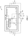
- FIG. 2 is a schematic representation of the system of FIG. 1 with example ground disconnections;
- FIG. 3 is a schematic representation of an IC package having first and second voltage domains and an impedance detector module for a differential capacitive detection
- FIG. 4A is a cross-sectional view showing layers of an IC package for detecting ground disconnections
- FIG. 4B shows an example pinout diagram for an IC package for detecting ground disconnections
- FIG. 5A is a cross-sectional view showing layers of a further IC package for detecting ground disconnections
- FIG. 5B is a cross-sectional view showing layers of a further IC package for detecting ground disconnections
- FIG. 6 is a schematic representation of a portion of a ground disconnection detection system including an impedance detector module
- FIG. 6A is an example comparison circuit for comparing a measured signal with a reference signal
- FIG. 6B is an example circuit for digitizing a measured signal for comparison with a threshold.
- FIG. 7 is a schematic representation of an example computer that can perform at least a portion of the processing described herein.
- FIG. 1 shows an example ground disconnection system 100 that can be implemented in an integrated circuit in accordance with example embodiments of the invention.
- a module 102 containing circuitry can include a first voltage domain module 104 and a second voltage domain module 106 .
- the first voltage domain module 104 operates at a first voltage level, such as 12V
- the second voltage domain module 106 operates at a second voltage level, such as 48V.
- An isolation barrier 107 which can be provided as a dielectric material, electrically isolates the first and second voltage domains 104 , 106 from each other.
- a first battery 108 which is shown as 12V, is connected to the first voltage domain module 104
- a second battery 110 which is shown as 48V, is coupled to the second voltage domain module 106 .
- Voltage levels of 12V and 48V are merely illustrative. It should be noted that certain automotive applications, including some hybrid vehicles, operate at 12V and 48V.
- a first ground 112 is connected to the first voltage domain module 104 and a second ground 114 is coupled to the second voltage domain module 106 .
- the first and second grounds 112 , 114 are coupled to a third ground 116 .
- the third ground 116 comprises chassis ground. That is, the third ground 116 is provided by a chassis of a vehicle. It is understood that the third ground 116 can be provided by any conductive structure that provides a suitable ground for the intended application.
- the first voltage domain module 104 includes an impedance detector module 118 configured to detect a disconnection of the first ground 112 connected to the first voltage domain module 104 and/or the second ground 114 connected to the second voltage domain module 106 .
- a detection component 120 which can comprise a capacitor, is coupled between the impedance detector module 118 and the first ground 112 .
- a barrier component 122 which can comprise a capacitor, is coupled between the first voltage domain module 104 and the second voltage domain module 106 .
- the barrier component 122 includes a capacitor having one plate 122 a located in the first voltage domain module 104 coupled to the impedance detector module 118 , and the other plate 122 b located in the second domain module 106 coupled to the second ground 114 .
- the detection capacitor 120 has first and second plates 120 a,b separated by a dielectric material.
- the detection component 120 and barrier component 122 are coupled in parallel with respect to chassis ground 116 .
- a disconnection or connection degradation e.g., rust, dirt, etc.
- the total impedance seen by the impedance detection module 118 will change.
- the total impedance seen by the impedance detection module 118 will increase due to a disconnection.
- FIG. 2 shows the system 100 of FIG. 1 with possible disconnection locations 130 a,b,c of the second ground 114 from chassis ground 116 .
- a first node 132 can be considered to be located at a point connecting the second voltage domain module 106 , the negative terminal of the second battery 110 , and the third (e.g., chassis) ground 116 .
- the first disconnection location 130 a is between the first node 132 and the barrier component 122 in the second voltage domain module 106 .
- the second disconnection location 130 b is between the first node 132 and the negative terminal of the second battery 110 .
- the third disconnection location 130 c is between the first node 132 and the third ground 116 . It understood that similar disconnection locations can occur for the first ground 112 .
- any disconnect or degradation at the disconnect locations 130 a,b,c will change the impedance seen by the impedance detector module 118 .
- a disconnect detection signal having selected characteristics, such as frequency and amplitude, can be injected into the circuit and the total impedance of the detection component 120 and barrier component 122 analyzed.
- a current level seen by the impedance detector module 118 can be monitored. In the event of a current threshold event, an alert can be generated on an I/O pin indicative of a ground disconnect detection.
- a sine wave is injected into the first and second voltage domains 104 , 106 .
- the impedance detector module 118 is connected to a positive terminal of one of the batteries and connected to the first and second batteries external to the impedance detector module. In example embodiments, the impedance detector module 118 injects a signal into the detection and barrier capacitors 120 , 122 . The portion of the injected signal in each of the capacitors depends on the relative impedance values of the capacitors.
- the impedance detector module 118 can be located in either of the first and second voltage domain modules 104 , 106 with a connection to corresponding one of the batteries 108 , 110 .
- an impedance detector located in the first voltage domain will be connected to the external battery source connected to the first voltage domain.
- FIG. 3 shows an alternative circuit implementation for a ground disconnection detection system in which like reference numbers indicated like elements.
- first and second barrier capacitors 140 , 142 each have a first terminal in the first voltage domain module 104 and a second terminal in the second voltage domain module 106 coupled to the second ground 114 .
- First and second detection capacitors 144 , 146 have respective first terminals separately coupled to the impedance detector module 118 and second terminals coupled to the first ground 112 .
- the first terminal of the first barrier capacitor 140 is coupled to the first terminal of the second detection capacitor 146 and the first terminal of the second barrier capacitor 142 is coupled to the first terminal of the first detection capacitor 144 . It is understood that the configuration of FIG. 3 injects a differential signal to minimize the effects of common-mode noise on the ground.
- the illustrative circuit of FIG. 1 can be implemented on an integrated circuit using silicon-in-insulator (SOI) processing, for example.
- SOI wafer contains a handle (base silicon), a buried oxide (BOX), and a device layer above the buried oxide.
- the device layer can be separated into a 12V side and a 48V side by a deep trench, that is etched down to and is connected to the buried oxide, and filled with SiO2, for example.
- the impedance detection circuit can be formed in the 12V device layer (e.g., first voltage domain), for example.
- Capacitor plates can be fabricated using various metal layers of the integrated circuit and metal interconnects.
- the dielectric of the capacitors can comprise inter-metal dielectric material, e.g., SiO2.
- the plates can be made from metal layers that overlap.
- the top plate of the barrier capacitor may span the trench from the detection node through a dielectric to a lower plate on the 48V side, which is connected to the 48V ground.
- the detection capacitor can have one plate connected to the detection node and the other plate connected to the 12V ground.
- metal plates on the same layer can be used to create a horizontal capacitor. It is understood that other combinations of metal layers can be used to create horizontal and/or vertical detection capacitors or barrier capacitors.
- One or more of the capacitor plates can be formed by using conductive polysilicon for either or both capacitors.
- FIGS. 4A and 4B show an example integrated circuit package implementation of the system 100 of FIG. 1 in which like reference numbers indicate like elements.
- a silicon substrate 200 includes a handle 202 having a first device layer 104 , which can correspond to the first voltage domain of FIG. 1 , and a second device layer 106 , which can correspond to the second voltage domain of FIG. 1 , separated from each other by a trench 107 filled with a dielectric material, such as SiO2.
- a layer 210 of insulating material, such as buried oxide known as BOX, is between the first and second device layers 104 , 106 and the handle 202 .
- circuitry is formed in the device layers of the substrate.
- first and second device layers 104 , 106 are formed from a single die. In other embodiments, first and second die are used with wirebonds between the first and second die to connect the plates of the barrier capacitor.
- a first metal layer 212 can be formed on the substrate and processed, e.g., etched, to form the second plate 120 b of the detection capacitor 120 and the second plate 122 b of the barrier capacitor 122 .
- the second plate 122 b of the barrier capacitor and the second plate 122 b of the detection capacitor are not connected to the respective device layers 104 , 106 .
- An inter-metal dielectric (IMD) layer 214 can be formed over the first metal layer 212 . It is understood that IMD layers can be formed by one of more applied layers of an insulator, such as SiO2, or other suitable materials/processes.
- a second metal layer 216 can be formed and processed to provide the first plate 120 a of the detection capacitor.
- a further IMD layer 218 can be formed on the second metal layer 216 and a third metal layer 220 can be formed to provide the first plate 122 a of the barrier capacitor 122 .
- a conductive material 222 can electrically connect the first plates 120 a , 122 a of the detection and barrier capacitors.
- the detection capacitor 120 shown in FIG. 4A represents the capacitor formed by plates 120 a , 120 b in the respective metal layers and that the barrier capacitor 122 shown represents the capacitor formed by plates 122 a , 122 b .
- the insulative material, such as SiO2, between the first plates 122 a , 120 a and second plates 120 b , 122 b can correspond to the barrier 107 of FIG. 1 .
- the first ground 112 shown as a 12V ground is coupled to the second plate 120 b of the detection capacitor 120 and the second ground, shown as a 48V ground, is coupled to the second plate 122 b of the detection capacitor.
- a 12V battery 108 can be coupled to the first device layer 104 and a 48V battery 110 can be coupled to the second device layer 106 .
- the impedance detection module 118 can be formed in the first device layer 104 and connected 230 to the first plate 120 a of the detection capacitor 120 . As described above, the impedance detection module 118 can generate an injection signal and measure signal levels, e.g., current, corresponding to the total impedance of the detection and barrier capacitors 120 , 122 for detecting a ground disconnection. In the event a ground disconnection is detected, the impedance detection module 118 can make active a ground disconnect detection (GGD) signal.
- GDD ground disconnect detection
- a variety of electrical configurations can be implemented in alternative IC packages.
- a variety of circuit components such as capacitors, inductors, resistors, etc., can be used in a range of circuit implementations to meet the needs of a particular application, such as providing a given circuit with desired impedance characteristics to enhance ground disconnect detection.
- FIG. 5A shows an alternative implementation of a ground disconnect detection IC in which common reference numbers indicate like elements.
- the barrier capacitor 122 ′ is capacitively coupled in a horizontal configuration.
- FIG. 5B shows a further implementation of a ground disconnect detection IC in which common reference numbers indicate like elements.
- the first plate 120 a of the detection capacitor 120 overlaps with the second plate 120 b of the detection capacitor, which is coupled to 12V ground, as well as a portion of the bulk substrate 202 , which forms the second plate 122 b of the barrier capacitor 122 .
- the dielectric material, including the trench material 107 and IMD layers between the bulk substrate 210 and the first plate 122 a provides the dielectric for the barrier capacitor 122 .
- the change in impedance causes current through the disconnect and barrier capacitors 120 , 122 to change when the injected signal is from a voltage source. If the injected signal is from a current source, then the voltages across the capacitors change.
- FIG. 6 is a schematic representation of an example impedance detector module 600 , such as the impedance detector module 118 of FIG. 1 .
- the impedance detector module 600 is connected to the detection capacitor 120 and the barrier capacitor 122 , as described above.
- a signal injection module 602 is configured to inject a signal into the detection capacitor 120 and the barrier capacitor 122 .
- a change in impedance due to a ground disconnect or connection degradation will change the signal through the detection capacitor 120 and the barrier capacitor 122 .
- a signal measurement module 604 can measure a current and/or voltage of a signal at a node between the detection capacitor 120 and the first ground 112 , for example.
- a signal processing module 606 can receive information from the signal measurement module 604 . If the injected signal from the signal injection module 602 is from a current source, then the voltages across the capacitors change. If the signal is above a current and/or voltage threshold, then the signal processing module 606 can activate the GDD (ground disconnect detection) signal.
- GDD ground disconnect detection
- any suitable circuitry can be used to detect a signal that exceeds/falls below a given threshold including sense resistors, comparators, analog-to-digital conversion, in an analog and/or digital domain.
- at least a portion of the circuitry for the impedance detection module 118 / 600 can be formed in an active layer of a die, such as the first and/or second device layers 104 , 106 described above.
- FIG. 6A shows an example of a measured signal MS in the signal measurement module 604 input to a comparator CMP or amplifier to generate an output signal. The measured signal MS is compared against a reference signal REF which corresponds to the threshold level to determine whether a GGD signal should be active.
- FIG. 6 shows a measured signal MS digitized by an analog-to-digital (ADC) for processing by a digital processor PROC.
- ADC analog-to-digital
- FIG. 7 shows an exemplary computer 700 that can perform at least part of the processing described herein, such as analyzing a measured signal during signal injection, as described above, to detect a ground disconnection.
- the computer 700 includes a processor 702 , a volatile memory 704 , a non-volatile memory 706 (e.g., hard disk), an output device 707 and a graphical user interface (GUI) 708 (e.g., a mouse, a keyboard, a display, for example).
- GUI graphical user interface
- the non-volatile memory 706 stores computer instructions 712 , an operating system 716 and data 718 .
- the computer instructions 712 are executed by the processor 702 out of volatile memory 704 .
- an article 720 comprises non-transitory computer-readable instructions.
- Processing may be implemented in hardware, software, or a combination of the two. Processing may be implemented in computer programs executed on programmable computers/machines that each includes a processor, a storage medium or other article of manufacture that is readable by the processor (including volatile and non-volatile memory and/or storage elements), at least one input device, and one or more output devices. Program code may be applied to data entered using an input device to perform processing and to generate output information.
- the system can perform processing, at least in part, via a computer program product, (e.g., in a machine-readable storage device), for execution by, or to control the operation of, data processing apparatus (e.g., a programmable processor, a computer, or multiple computers).
- a computer program product e.g., in a machine-readable storage device
- data processing apparatus e.g., a programmable processor, a computer, or multiple computers.
- Each such program may be implemented in a high-level procedural or object-oriented programming language to communicate with a computer system.
- the programs may be implemented in assembly or machine language.
- the language may be a compiled or an interpreted language and it may be deployed in any form, including as a stand-alone program or as a module, component, subroutine, or other unit suitable for use in a computing environment.
- a computer program may be deployed to be executed on one computer or on multiple computers at one site or distributed across multiple sites and interconnected by a communication network.
- a computer program may be stored on a storage medium or device (e.g., CD-ROM, hard disk, or magnetic diskette) that is readable by a general or special purpose programmable computer for configuring and operating the computer when the storage medium or device is read by the computer.
- Processing may also be implemented as a machine-readable storage medium, configured with a computer program, where upon execution, instructions in the computer program cause the computer to operate.
- Processing may be performed by one or more programmable processors executing one or more computer programs to perform the functions of the system. All or part of the system may be implemented as, special purpose logic circuitry (e.g., an FPGA (field programmable gate array) and/or an ASIC (application-specific integrated circuit)).
- special purpose logic circuitry e.g., an FPGA (field programmable gate array) and/or an ASIC (application-specific integrated circuit)
Landscapes
- Physics & Mathematics (AREA)
- General Physics & Mathematics (AREA)
- Chemical & Material Sciences (AREA)
- Engineering & Computer Science (AREA)
- Combustion & Propulsion (AREA)
- Testing Of Short-Circuits, Discontinuities, Leakage, Or Incorrect Line Connections (AREA)
Abstract
Description
Claims (33)
Priority Applications (2)
| Application Number | Priority Date | Filing Date | Title |
|---|---|---|---|
| US16/539,405 US11029366B2 (en) | 2019-08-13 | 2019-08-13 | Ground disconnect detection for multiple voltage domains |
| EP20187369.2A EP3779478B1 (en) | 2019-08-13 | 2020-07-23 | Ground disconnect detection for multiple voltage domains |
Applications Claiming Priority (1)
| Application Number | Priority Date | Filing Date | Title |
|---|---|---|---|
| US16/539,405 US11029366B2 (en) | 2019-08-13 | 2019-08-13 | Ground disconnect detection for multiple voltage domains |
Publications (2)
| Publication Number | Publication Date |
|---|---|
| US20210048467A1 US20210048467A1 (en) | 2021-02-18 |
| US11029366B2 true US11029366B2 (en) | 2021-06-08 |
Family
ID=72050644
Family Applications (1)
| Application Number | Title | Priority Date | Filing Date |
|---|---|---|---|
| US16/539,405 Active 2040-02-26 US11029366B2 (en) | 2019-08-13 | 2019-08-13 | Ground disconnect detection for multiple voltage domains |
Country Status (2)
| Country | Link |
|---|---|
| US (1) | US11029366B2 (en) |
| EP (1) | EP3779478B1 (en) |
Cited By (4)
| Publication number | Priority date | Publication date | Assignee | Title |
|---|---|---|---|---|
| US11721648B2 (en) | 2019-06-04 | 2023-08-08 | Allegro Microsystems, Llc | Signal isolator having at least one isolation island |
| US12199586B2 (en) | 2023-03-30 | 2025-01-14 | Allegro Microsystems, Llc | Capacitive isolator having common mode noise suppression |
| US12244277B2 (en) | 2022-03-04 | 2025-03-04 | Allegro Microsystems, Llc | Common mode transient suppression |
| US12557561B2 (en) | 2022-06-16 | 2026-02-17 | Allegro Microsystems, Llc | Hall effect device with trench about a micron or greater in depth |
Families Citing this family (4)
| Publication number | Priority date | Publication date | Assignee | Title |
|---|---|---|---|---|
| US20210057330A1 (en) * | 2019-08-22 | 2021-02-25 | Allegro Microsystems, Llc | Single chip signal isolator |
| US11515246B2 (en) | 2020-10-09 | 2022-11-29 | Allegro Microsystems, Llc | Dual circuit digital isolator |
| CN114019413B (en) * | 2021-11-04 | 2022-09-06 | 上海交通大学 | Monopole ground fault distance measurement method based on sub-module short-time active locking |
| EP4466767A1 (en) * | 2022-01-17 | 2024-11-27 | Punch Powertrain N.V. | Safety circuit, power converter and power system |
Citations (30)
| Publication number | Priority date | Publication date | Assignee | Title |
|---|---|---|---|---|
| US5812363A (en) | 1996-05-09 | 1998-09-22 | Murata Manufacturing Co., Ltd. | Multilayer capacitor including a dielectric breakdown prevention layer |
| US20040189323A1 (en) | 2003-03-31 | 2004-09-30 | Kazuyoshi Nagase | Disconnection detecting circuit for sensor apparatus |
| US6873065B2 (en) | 1997-10-23 | 2005-03-29 | Analog Devices, Inc. | Non-optical signal isolator |
| US20060263727A1 (en) | 2005-05-18 | 2006-11-23 | Megica Corporation | Semiconductor chip with coil element over passivation layer |
| US20080158777A1 (en) | 2006-12-29 | 2008-07-03 | Samsung Electro-Mechanics Co., Ltd | Capacitor and multi-layer board embedding the capacitor |
| US20090278547A1 (en) | 2008-05-08 | 2009-11-12 | Lear Corporation | Ground-fault detection system for vehicles with a high-voltage power net |
| US20100244849A1 (en) | 2009-03-31 | 2010-09-30 | Honda Motor Co., Ltd. | Electric vehicle with ground fault detecting system |
| US20110148549A1 (en) | 2009-12-23 | 2011-06-23 | Peter Kanschat | Signal Transmission Arrangement |
| US8169108B2 (en) | 2004-06-03 | 2012-05-01 | Silicon Laboratories Inc. | Capacitive isolator |
| US20120181874A1 (en) | 2011-01-18 | 2012-07-19 | Stefan Willkofer | Semiconductor Device and Method of Manufacture Thereof |
| US20130229734A1 (en) | 2009-10-02 | 2013-09-05 | Semicomductor Components Industries, LLC | Ground fault circuit interrupter and method |
| US20130278372A1 (en) | 2012-04-20 | 2013-10-24 | Infineon Technologies Austria Ag | Semiconductor Component with Coreless Transformer |
| US20130278077A1 (en) | 2012-04-23 | 2013-10-24 | Analog Devices, Inc. | Isolated measurement system with cooperatively-timed isolated power generation |
| US20130300430A1 (en) | 2012-05-09 | 2013-11-14 | Curtis Instruments, Inc. | Isolation monitor |
| US20130335882A1 (en) | 2012-06-14 | 2013-12-19 | Uchicago Argonne, Llc. | Method of making dielectric capacitors with increased dielectric breakdown strength |
| US8643138B2 (en) | 2011-06-30 | 2014-02-04 | Silicon Laboratories Inc. | High breakdown voltage integrated circuit isolation structure |
| US20140049261A1 (en) | 2011-04-28 | 2014-02-20 | Aerovironment, Inc. | Pulsed missing ground detector circuit |
| DE102013100622A1 (en) | 2013-01-22 | 2014-07-24 | Phoenix Contact Gmbh & Co. Kg | Printed circuit board in layer construction |
| US20140253225A1 (en) | 2013-03-10 | 2014-09-11 | Microchip Technology Incorporated | Method and Apparatus for Generating Regulated Isolation Supply Voltage |
| US20140253227A1 (en) | 2013-03-10 | 2014-09-11 | Microchip Technology Incorporated | Integrated High Voltage Isolation Using Low Value Capacitors |
| US8937797B2 (en) | 2012-03-19 | 2015-01-20 | Allegro Microsystems, Llc | Method and apparatus to detect a broken wire condition in an integrated circuit |
| US20150219706A1 (en) | 2013-08-31 | 2015-08-06 | Ford Global Technologies, Llc | Vehicle High-Voltage Systems Isolation Testing |
| US20150233859A1 (en) | 2014-02-14 | 2015-08-20 | Peng Zhu | Impedance detection circuit, method, and integrated circuit |
| US20160126367A1 (en) | 2009-10-19 | 2016-05-05 | Helios Focus Llc | Solar Photovaltaic Module Rapid Shutdown and Safety System |
| US9514879B2 (en) | 2009-10-21 | 2016-12-06 | Stmicroelectronics S.R.L. | Signal transmission through LC resonant circuits |
| US9660848B2 (en) | 2014-09-15 | 2017-05-23 | Analog Devices Global | Methods and structures to generate on/off keyed carrier signals for signal isolators |
| US20170250127A1 (en) * | 2010-12-13 | 2017-08-31 | Infineon Technologies Americas Corp. | Semiconductor package having multi-phase power inverter with internal temperature sensor |
| US9824995B2 (en) * | 2014-09-29 | 2017-11-21 | Nxp Usa, Inc. | Flexible circuit leads in packaging for radio frequency devices |
| US10074939B1 (en) | 2017-08-08 | 2018-09-11 | Allegro Microsystems, Llc | Signal isolator having inductive and capacitive signal coupling |
| US20190371746A1 (en) * | 2018-06-01 | 2019-12-05 | Analog Devices, Inc. | Matching circuit for integrated circuit die |
-
2019
- 2019-08-13 US US16/539,405 patent/US11029366B2/en active Active
-
2020
- 2020-07-23 EP EP20187369.2A patent/EP3779478B1/en active Active
Patent Citations (30)
| Publication number | Priority date | Publication date | Assignee | Title |
|---|---|---|---|---|
| US5812363A (en) | 1996-05-09 | 1998-09-22 | Murata Manufacturing Co., Ltd. | Multilayer capacitor including a dielectric breakdown prevention layer |
| US6873065B2 (en) | 1997-10-23 | 2005-03-29 | Analog Devices, Inc. | Non-optical signal isolator |
| US20040189323A1 (en) | 2003-03-31 | 2004-09-30 | Kazuyoshi Nagase | Disconnection detecting circuit for sensor apparatus |
| US8169108B2 (en) | 2004-06-03 | 2012-05-01 | Silicon Laboratories Inc. | Capacitive isolator |
| US20060263727A1 (en) | 2005-05-18 | 2006-11-23 | Megica Corporation | Semiconductor chip with coil element over passivation layer |
| US20080158777A1 (en) | 2006-12-29 | 2008-07-03 | Samsung Electro-Mechanics Co., Ltd | Capacitor and multi-layer board embedding the capacitor |
| US20090278547A1 (en) | 2008-05-08 | 2009-11-12 | Lear Corporation | Ground-fault detection system for vehicles with a high-voltage power net |
| US20100244849A1 (en) | 2009-03-31 | 2010-09-30 | Honda Motor Co., Ltd. | Electric vehicle with ground fault detecting system |
| US20130229734A1 (en) | 2009-10-02 | 2013-09-05 | Semicomductor Components Industries, LLC | Ground fault circuit interrupter and method |
| US20160126367A1 (en) | 2009-10-19 | 2016-05-05 | Helios Focus Llc | Solar Photovaltaic Module Rapid Shutdown and Safety System |
| US9514879B2 (en) | 2009-10-21 | 2016-12-06 | Stmicroelectronics S.R.L. | Signal transmission through LC resonant circuits |
| US20110148549A1 (en) | 2009-12-23 | 2011-06-23 | Peter Kanschat | Signal Transmission Arrangement |
| US20170250127A1 (en) * | 2010-12-13 | 2017-08-31 | Infineon Technologies Americas Corp. | Semiconductor package having multi-phase power inverter with internal temperature sensor |
| US20120181874A1 (en) | 2011-01-18 | 2012-07-19 | Stefan Willkofer | Semiconductor Device and Method of Manufacture Thereof |
| US20140049261A1 (en) | 2011-04-28 | 2014-02-20 | Aerovironment, Inc. | Pulsed missing ground detector circuit |
| US8643138B2 (en) | 2011-06-30 | 2014-02-04 | Silicon Laboratories Inc. | High breakdown voltage integrated circuit isolation structure |
| US8937797B2 (en) | 2012-03-19 | 2015-01-20 | Allegro Microsystems, Llc | Method and apparatus to detect a broken wire condition in an integrated circuit |
| US20130278372A1 (en) | 2012-04-20 | 2013-10-24 | Infineon Technologies Austria Ag | Semiconductor Component with Coreless Transformer |
| US20130278077A1 (en) | 2012-04-23 | 2013-10-24 | Analog Devices, Inc. | Isolated measurement system with cooperatively-timed isolated power generation |
| US20130300430A1 (en) | 2012-05-09 | 2013-11-14 | Curtis Instruments, Inc. | Isolation monitor |
| US20130335882A1 (en) | 2012-06-14 | 2013-12-19 | Uchicago Argonne, Llc. | Method of making dielectric capacitors with increased dielectric breakdown strength |
| DE102013100622A1 (en) | 2013-01-22 | 2014-07-24 | Phoenix Contact Gmbh & Co. Kg | Printed circuit board in layer construction |
| US20140253227A1 (en) | 2013-03-10 | 2014-09-11 | Microchip Technology Incorporated | Integrated High Voltage Isolation Using Low Value Capacitors |
| US20140253225A1 (en) | 2013-03-10 | 2014-09-11 | Microchip Technology Incorporated | Method and Apparatus for Generating Regulated Isolation Supply Voltage |
| US20150219706A1 (en) | 2013-08-31 | 2015-08-06 | Ford Global Technologies, Llc | Vehicle High-Voltage Systems Isolation Testing |
| US20150233859A1 (en) | 2014-02-14 | 2015-08-20 | Peng Zhu | Impedance detection circuit, method, and integrated circuit |
| US9660848B2 (en) | 2014-09-15 | 2017-05-23 | Analog Devices Global | Methods and structures to generate on/off keyed carrier signals for signal isolators |
| US9824995B2 (en) * | 2014-09-29 | 2017-11-21 | Nxp Usa, Inc. | Flexible circuit leads in packaging for radio frequency devices |
| US10074939B1 (en) | 2017-08-08 | 2018-09-11 | Allegro Microsystems, Llc | Signal isolator having inductive and capacitive signal coupling |
| US20190371746A1 (en) * | 2018-06-01 | 2019-12-05 | Analog Devices, Inc. | Matching circuit for integrated circuit die |
Non-Patent Citations (15)
| Title |
|---|
| Akiyama et al., "A High-Voltage Monolithic Isolator for a Communication Network Interface;" IEEE Transactions on Electron Devices, vol. 49, No. 5; May 2002; 7 Pages. |
| Culurciello et al., "Monolithic Digital Galvanic Isolation Buffer Fabricated in Silicon on Sapphire CMOS;" Electronic Letters, vol. 41, No. 9; Apr. 28, 2005; 2 Pages. |
| Daughton, "Spin-Dependent Sensors;" Invited Paper; Proceedings of the IEEE, vol. 91, No. 5; May 2003; 6 Pages. |
| European Examination Report dated Sep. 26, 2019 for European Application No. 18185696.4; 4 Pages. |
| European Intention to Grant dated Apr. 20, 2020 for European Application No. 18185696.4; 6 Pages. |
| Extended European Search Report (EESR) dated Jan. 15, 2021 for European Application No. 20187369.2; 9 Pages. |
| Extended European Search Report dated Jan. 4, 2019 for European Application No. 18185696.4; 5 Pages. |
| Knoedl, Jr. et al., "A Monolithic Signal Isolator;" Proceedings of the 4th Annual IEEE Applied Power Electronics Conference and Exposition; Mar. 13, 1989; pp. 165-170; 6 Pages. |
| Moghe et al., "Monolithic 2.5kV RMS, 1.8V-3.3V Dual Channel 640Mbps Digital Isolator in 0.5μm SOS;" Proceedings of the IEEE International SOI Conference; Oct. 1, 2012; 2 Pages. |
| Response (with Amended Claims) to European Examination Report dated Sep. 26, 2019 for European Application No. 18185696.4; Response filed Jan. 13, 2020; 7 Pages. |
| Response (with Amended Specification & Claims) to Extended European Search Report dated Jan. 4, 2019 for European Application No. 18185696.4; Response filed Jun. 4, 2019; 14 Pages. |
| U.S. Appl. No. 15/906,291, filed Feb. 27, 2018, Briano et al. |
| U.S. Appl. No. 16/430,849, filed Jun. 4, 2019, Briano et al. |
| U.S. Appl. No. 16/547,823, filed Aug. 22, 2019, Briano et al. |
| U.S. Notice of Allowance dated Jun. 13, 2018 for U.S. Appl. No. 15/671,357; 12 Pages. |
Cited By (4)
| Publication number | Priority date | Publication date | Assignee | Title |
|---|---|---|---|---|
| US11721648B2 (en) | 2019-06-04 | 2023-08-08 | Allegro Microsystems, Llc | Signal isolator having at least one isolation island |
| US12244277B2 (en) | 2022-03-04 | 2025-03-04 | Allegro Microsystems, Llc | Common mode transient suppression |
| US12557561B2 (en) | 2022-06-16 | 2026-02-17 | Allegro Microsystems, Llc | Hall effect device with trench about a micron or greater in depth |
| US12199586B2 (en) | 2023-03-30 | 2025-01-14 | Allegro Microsystems, Llc | Capacitive isolator having common mode noise suppression |
Also Published As
| Publication number | Publication date |
|---|---|
| US20210048467A1 (en) | 2021-02-18 |
| EP3779478B1 (en) | 2023-10-18 |
| EP3779478A1 (en) | 2021-02-17 |
Similar Documents
| Publication | Publication Date | Title |
|---|---|---|
| US11029366B2 (en) | Ground disconnect detection for multiple voltage domains | |
| US10811327B2 (en) | Die edge integrity monitoring system | |
| US10109601B2 (en) | Integrated circuit with detection of thinning via the back face and decoupling capacitors | |
| JP5955951B2 (en) | Integrated circuits for capacitance measurements including floating bridges. | |
| US8809858B2 (en) | Device for protecting an integrated circuit against back side attacks | |
| US20210057330A1 (en) | Single chip signal isolator | |
| US20020027488A1 (en) | Method and system for isolated coupling | |
| US11112465B2 (en) | Integrated circuit having insulation monitoring with frequency discrimination | |
| US11733289B2 (en) | Chip crack detection apparatus | |
| US7352201B2 (en) | System and method for testing devices utilizing capacitively coupled signaling | |
| CN206685382U (en) | Electronic chip | |
| US8014113B2 (en) | Protection for proximity electronics against electrostatic discharge | |
| US20180045764A1 (en) | Semiconductor circuits, devices and methods | |
| US9476924B2 (en) | Sensor system and method for reducing a settling time of a sensor system | |
| KR102054165B1 (en) | Single Photon Detector, Avalanche Photodiode for Single Photon Detector and Circuit Board Connected to the Same | |
| CN103872023A (en) | Structure and method for testing performances of inter-layer dielectric layer | |
| US5182531A (en) | Interference protected electronic apparatus | |
| KR102838214B1 (en) | Capacitive sensor | |
| US11971445B2 (en) | Integrated circuit and associated method | |
| Yao et al. | Electromagnetic noise coupling and mitigation in dynamic tests of high power switching devices | |
| JP5066687B2 (en) | Impedance measurement circuit for minute conduction region and impedance measurement method for minute conduction region | |
| Schröter et al. | Improving the immunity of automotive ICs by controlling RF substrate coupling | |
| US11131782B2 (en) | Ionizing radiation detector | |
| Sowariraj et al. | A 3-D Circuit Model to evaluate CDM performance of ICs |
Legal Events
| Date | Code | Title | Description |
|---|---|---|---|
| FEPP | Fee payment procedure |
Free format text: ENTITY STATUS SET TO UNDISCOUNTED (ORIGINAL EVENT CODE: BIG.); ENTITY STATUS OF PATENT OWNER: LARGE ENTITY |
|
| AS | Assignment |
Owner name: ALLEGRO MICROSYSTEMS, LLC, NEW HAMPSHIRE Free format text: ASSIGNMENT OF ASSIGNORS INTEREST;ASSIGNOR:BRIANO, ROBERT A.;REEL/FRAME:050089/0110 Effective date: 20190813 |
|
| AS | Assignment |
Owner name: MIZUHO BANK LTD., AS COLLATERAL AGENT, NEW YORK Free format text: PATENT SECURITY AGREEMENT;ASSIGNOR:ALLEGRO MICROSYSTEMS, LLC;REEL/FRAME:053957/0620 Effective date: 20200930 Owner name: CREDIT SUISSE AG, CAYMAN ISLANDS BRANCH, AS COLLATERAL AGENT, NEW YORK Free format text: PATENT SECURITY AGREEMENT;ASSIGNOR:ALLEGRO MICROSYSTEMS, LLC;REEL/FRAME:053957/0874 Effective date: 20200930 |
|
| STPP | Information on status: patent application and granting procedure in general |
Free format text: NOTICE OF ALLOWANCE MAILED -- APPLICATION RECEIVED IN OFFICE OF PUBLICATIONS |
|
| STPP | Information on status: patent application and granting procedure in general |
Free format text: PUBLICATIONS -- ISSUE FEE PAYMENT RECEIVED |
|
| STPP | Information on status: patent application and granting procedure in general |
Free format text: PUBLICATIONS -- ISSUE FEE PAYMENT VERIFIED |
|
| STCF | Information on status: patent grant |
Free format text: PATENTED CASE |
|
| AS | Assignment |
Owner name: ALLEGRO MICROSYSTEMS, LLC, NEW HAMPSHIRE Free format text: RELEASE OF SECURITY INTEREST IN PATENTS (R/F 053957/0620);ASSIGNOR:MIZUHO BANK, LTD., AS COLLATERAL AGENT;REEL/FRAME:064068/0360 Effective date: 20230621 Owner name: MORGAN STANLEY SENIOR FUNDING, INC., AS THE COLLATERAL AGENT, MARYLAND Free format text: PATENT SECURITY AGREEMENT;ASSIGNOR:ALLEGRO MICROSYSTEMS, LLC;REEL/FRAME:064068/0459 Effective date: 20230621 |
|
| AS | Assignment |
Owner name: ALLEGRO MICROSYSTEMS, LLC, NEW HAMPSHIRE Free format text: RELEASE OF SECURITY INTEREST IN PATENTS AT REEL 053957/FRAME 0874;ASSIGNOR:CREDIT SUISSE AG, CAYMAN ISLANDS BRANCH, AS COLLATERAL AGENT;REEL/FRAME:065420/0572 Effective date: 20231031 |
|
| MAFP | Maintenance fee payment |
Free format text: PAYMENT OF MAINTENANCE FEE, 4TH YEAR, LARGE ENTITY (ORIGINAL EVENT CODE: M1551); ENTITY STATUS OF PATENT OWNER: LARGE ENTITY Year of fee payment: 4 |