US11011732B2 - Organic light emitting diode display device - Google Patents
Organic light emitting diode display device Download PDFInfo
- Publication number
- US11011732B2 US11011732B2 US16/148,274 US201816148274A US11011732B2 US 11011732 B2 US11011732 B2 US 11011732B2 US 201816148274 A US201816148274 A US 201816148274A US 11011732 B2 US11011732 B2 US 11011732B2
- Authority
- US
- United States
- Prior art keywords
- disposed
- reflective
- light emitting
- electrode
- organic light
- Prior art date
- Legal status (The legal status is an assumption and is not a legal conclusion. Google has not performed a legal analysis and makes no representation as to the accuracy of the status listed.)
- Active
Links
Images


Classifications
-
- H01L51/5271—
-
- H—ELECTRICITY
- H10—SEMICONDUCTOR DEVICES; ELECTRIC SOLID-STATE DEVICES NOT OTHERWISE PROVIDED FOR
- H10K—ORGANIC ELECTRIC SOLID-STATE DEVICES
- H10K59/00—Integrated devices, or assemblies of multiple devices, comprising at least one organic light-emitting element covered by group H10K50/00
- H10K59/80—Constructional details
- H10K59/875—Arrangements for extracting light from the devices
- H10K59/878—Arrangements for extracting light from the devices comprising reflective means
-
- H—ELECTRICITY
- H10—SEMICONDUCTOR DEVICES; ELECTRIC SOLID-STATE DEVICES NOT OTHERWISE PROVIDED FOR
- H10K—ORGANIC ELECTRIC SOLID-STATE DEVICES
- H10K59/00—Integrated devices, or assemblies of multiple devices, comprising at least one organic light-emitting element covered by group H10K50/00
- H10K59/10—OLED displays
- H10K59/12—Active-matrix OLED [AMOLED] displays
- H10K59/121—Active-matrix OLED [AMOLED] displays characterised by the geometry or disposition of pixel elements
- H10K59/1213—Active-matrix OLED [AMOLED] displays characterised by the geometry or disposition of pixel elements the pixel elements being TFTs
-
- H01L27/3258—
-
- H01L27/3276—
-
- H—ELECTRICITY
- H10—SEMICONDUCTOR DEVICES; ELECTRIC SOLID-STATE DEVICES NOT OTHERWISE PROVIDED FOR
- H10K—ORGANIC ELECTRIC SOLID-STATE DEVICES
- H10K50/00—Organic light-emitting devices
- H10K50/80—Constructional details
- H10K50/85—Arrangements for extracting light from the devices
- H10K50/856—Arrangements for extracting light from the devices comprising reflective means
-
- H—ELECTRICITY
- H10—SEMICONDUCTOR DEVICES; ELECTRIC SOLID-STATE DEVICES NOT OTHERWISE PROVIDED FOR
- H10K—ORGANIC ELECTRIC SOLID-STATE DEVICES
- H10K59/00—Integrated devices, or assemblies of multiple devices, comprising at least one organic light-emitting element covered by group H10K50/00
- H10K59/10—OLED displays
- H10K59/12—Active-matrix OLED [AMOLED] displays
- H10K59/122—Pixel-defining structures or layers, e.g. banks
-
- H—ELECTRICITY
- H10—SEMICONDUCTOR DEVICES; ELECTRIC SOLID-STATE DEVICES NOT OTHERWISE PROVIDED FOR
- H10K—ORGANIC ELECTRIC SOLID-STATE DEVICES
- H10K59/00—Integrated devices, or assemblies of multiple devices, comprising at least one organic light-emitting element covered by group H10K50/00
- H10K59/10—OLED displays
- H10K59/12—Active-matrix OLED [AMOLED] displays
- H10K59/124—Insulating layers formed between TFT elements and OLED elements
-
- H—ELECTRICITY
- H10—SEMICONDUCTOR DEVICES; ELECTRIC SOLID-STATE DEVICES NOT OTHERWISE PROVIDED FOR
- H10K—ORGANIC ELECTRIC SOLID-STATE DEVICES
- H10K59/00—Integrated devices, or assemblies of multiple devices, comprising at least one organic light-emitting element covered by group H10K50/00
- H10K59/10—OLED displays
- H10K59/12—Active-matrix OLED [AMOLED] displays
- H10K59/131—Interconnections, e.g. wiring lines or terminals
-
- H—ELECTRICITY
- H10—SEMICONDUCTOR DEVICES; ELECTRIC SOLID-STATE DEVICES NOT OTHERWISE PROVIDED FOR
- H10K—ORGANIC ELECTRIC SOLID-STATE DEVICES
- H10K59/00—Integrated devices, or assemblies of multiple devices, comprising at least one organic light-emitting element covered by group H10K50/00
- H10K59/30—Devices specially adapted for multicolour light emission
- H10K59/35—Devices specially adapted for multicolour light emission comprising red-green-blue [RGB] subpixels
-
- H—ELECTRICITY
- H10—SEMICONDUCTOR DEVICES; ELECTRIC SOLID-STATE DEVICES NOT OTHERWISE PROVIDED FOR
- H10K—ORGANIC ELECTRIC SOLID-STATE DEVICES
- H10K59/00—Integrated devices, or assemblies of multiple devices, comprising at least one organic light-emitting element covered by group H10K50/00
- H10K59/30—Devices specially adapted for multicolour light emission
- H10K59/38—Devices specially adapted for multicolour light emission comprising colour filters or colour changing media [CCM]
-
- H01L27/322—
-
- H01L27/3246—
-
- H01L27/3279—
-
- H01L51/525—
-
- H—ELECTRICITY
- H10—SEMICONDUCTOR DEVICES; ELECTRIC SOLID-STATE DEVICES NOT OTHERWISE PROVIDED FOR
- H10K—ORGANIC ELECTRIC SOLID-STATE DEVICES
- H10K50/00—Organic light-emitting devices
- H10K50/80—Constructional details
- H10K50/84—Passivation; Containers; Encapsulations
- H10K50/842—Containers
- H10K50/8428—Vertical spacers, e.g. arranged between the sealing arrangement and the OLED
-
- H—ELECTRICITY
- H10—SEMICONDUCTOR DEVICES; ELECTRIC SOLID-STATE DEVICES NOT OTHERWISE PROVIDED FOR
- H10K—ORGANIC ELECTRIC SOLID-STATE DEVICES
- H10K59/00—Integrated devices, or assemblies of multiple devices, comprising at least one organic light-emitting element covered by group H10K50/00
- H10K59/10—OLED displays
- H10K59/12—Active-matrix OLED [AMOLED] displays
- H10K59/131—Interconnections, e.g. wiring lines or terminals
- H10K59/1315—Interconnections, e.g. wiring lines or terminals comprising structures specially adapted for lowering the resistance
-
- H—ELECTRICITY
- H10—SEMICONDUCTOR DEVICES; ELECTRIC SOLID-STATE DEVICES NOT OTHERWISE PROVIDED FOR
- H10K—ORGANIC ELECTRIC SOLID-STATE DEVICES
- H10K59/00—Integrated devices, or assemblies of multiple devices, comprising at least one organic light-emitting element covered by group H10K50/00
- H10K59/80—Constructional details
- H10K59/87—Passivation; Containers; Encapsulations
- H10K59/871—Self-supporting sealing arrangements
- H10K59/8723—Vertical spacers, e.g. arranged between the sealing arrangement and the OLED
-
- H—ELECTRICITY
- H10—SEMICONDUCTOR DEVICES; ELECTRIC SOLID-STATE DEVICES NOT OTHERWISE PROVIDED FOR
- H10K—ORGANIC ELECTRIC SOLID-STATE DEVICES
- H10K59/00—Integrated devices, or assemblies of multiple devices, comprising at least one organic light-emitting element covered by group H10K50/00
- H10K59/80—Constructional details
- H10K59/87—Passivation; Containers; Encapsulations
- H10K59/873—Encapsulations
Definitions
- the present disclosure relates to an organic light emitting diode display device, and more particularly, to an organic light emitting diode display device having improved light extraction efficiency.
- the flat display devices there are a liquid crystal display (LCD) device, a plasma display panel (PDP) device, a field emission display (FED) device, an electroluminescence display (ELD) device, an organic light emitting diode (OLED) display device, and the like.
- LCD liquid crystal display
- PDP plasma display panel
- FED field emission display
- ELD electroluminescence display
- OLED organic light emitting diode
- the flat display devices exhibit excellent characteristics in terms of thinning, lightening, and reductions in the power consumption thereof and thus have rapidly replaced the conventional cathode ray tube (CRT) displays.
- CTR cathode ray tube
- the OLED display device is an emissive type device and does not require a backlight unit used in a non-emissive type device, i.e., the LCD device.
- the OLED display device has light weight and a thin profile.
- the OLED display device has advantages of a viewing angle, a contrast ratio, and power consumption as compared with the LCD device. Furthermore, the OLED display device may be driven with a low direct current (DC) voltage and has rapid response speed. Moreover, since inner elements of the OLED display device have a solid phase, the OLED display device has high durability against an external impact and has a wide available temperature range.
- DC direct current
- the OLED display device is manufactured through a simple process, manufacturing costs may be reduced as compared with the conventional LCD device.
- the OLED display device is an emissive type device emitting light through a light emitting diode (LED).
- the LED emits light through an organic electroluminescence phenomenon.
- FIG. 1 is a band diagram illustrating an LED having an emission principle based on a general organic electroluminescence phenomenon.
- an LED 10 includes an anode 21 , a cathode 25 , and an organic light emitting layer disposed between the anode 21 and the cathode 25 .
- the organic light emitting layer includes a hole transport layer (HTL) 33 , an electron transport layer (ETL) 35 , and an emission material layer (EML) 40 interposed between the HTL 33 and the ETL 35 .
- HTL hole transport layer
- ETL electron transport layer
- EML emission material layer
- HIL hole injection layer
- EIL electron injection layer
- an amount of the light emitted from the organic light emitting layer is increased along with an amount of a current applied to the OLED display device, it is possible to further increase brightness of the OLED display device by applying more currents to the organic light emitting layer. However, in this case, power consumption is increased, and lifetime of the OLED display device is also reduced.
- the present disclosure has been made to solve the above problems and is directed to providing an organic light emitting diode display having improved light extraction efficiency.
- the present disclosure is directed to preventing light leakage.
- the present disclosure provides an organic light emitting diode display device including: a substrate having a plurality of subpixels which each have an emission region and a non-emission region defined along an edge of the emission region; a reflective barrier disposed to correspond to the non-emission region and including a reflective side surface; an overcoat layer disposed on an upper portion of the reflective barrier; and a light emitting diode including a first electrode, an organic light emitting layer, and a second electrode, which are sequentially disposed on the overcoat layer, wherein the reflective side surface of the reflective barrier is inversely tapered such that a width thereof is decreased in a traveling direction of light emitted from the organic light emitting layer.
- FIG. 1 is a band diagram illustrating a light emitting diode (LED) having an emission principle based on an organic electroluminescence phenomenon according to the related art.
- LED light emitting diode
- FIG. 2 is a plan view illustrating a structure of one unit pixel including three subpixels in an organic light emitting diode (OLED) display device according to an embodiment of the present disclosure.
- OLED organic light emitting diode
- FIG. 3 is a cross-sectional view taken along line III-III of FIG. 2 illustrating a structure of one unit pixel P including three subpixels in the OLED display device according to an embodiment of the present disclosure.
- FIG. 4 is a schematic view illustrating a state in which light is guided in the OLED display device according to an embodiment of the present disclosure.
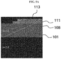
- FIG. 5A illustrates a simulation result of measuring a state in which light is guided in an OLED display device not including a reflective barrier.
- FIGS. 5B to 5E illustrate simulation results of measuring a state in which light is guided in the OLED display device including a reflective barrier according to embodiments of the present disclosure.
- FIG. 6 is a schematic cross-sectional view illustrating a reflective barrier according to an embodiment of the present disclosure.
- FIG. 2 is a plan view illustrating a structure of one unit pixel including three subpixels in an organic light emitting diode (OLED) display device according to an embodiment of the present disclosure.
- OLED organic light emitting diode
- FIG. 3 is a cross-sectional view taken along line III-III of FIG. 2 , illustrating a structure of one unit pixel P including three subpixels R-SP, G-SP, and B-SP in the OLED display device according to the embodiment of the present disclosure.
- an OLED display device 100 Prior to the description, an OLED display device 100 according to an embodiment of the present disclosure is classified into a top emission type or a bottom emission type according to a transmission direction of emitted light.
- the bottom emission type will be described as an example in the present disclosure.
- one unit pixel P includes red, green, and blue subpixels R-SP, G-SP, and B-SP.
- Each of the subpixels R-SP, G-SP, and B-SP includes an emission region EA.
- a bank 119 is disposed along an edge of the emission region EA to constitute a non-emission region NEA.
- the subpixels R-SP, G-SP, and B-SP are illustrated as having the same width and being disposed in parallel to each other.
- the subpixels R-SP, G-SP, and B-SP may have different widths and various structures.
- switching and driving thin film transistors STr and DTr are provided in the non-emission region NEA of each of the subpixels R-SP, G-SP, and B-SP.
- a light emitting diode (LED) E including a first electrode 111 , an organic light emitting layer 113 , and a second electrode 115 are disposed in the emission region EA in each of the subpixels R-SP, G-SP, and B-SP.
- the switching thin film transistor STr and the driving thin film transistor DTr are connected to each other, and the driving thin film transistor DTr is connected to the LED E.
- gate lines GL, data lines DL, and power lines VDD are disposed on a substrate 101 to define the subpixels R-SP, G-SP, and B-SP.
- the switching thin film transistor STr is formed at a portion where the gate line GL and the data line DL cross each other.
- the switching thin film transistor STr functions to select the subpixels R-SP, G-SP, and B-SP.
- the switching thin film transistor STr includes a gate electrode SG branched from the gate line GL, a semiconductor layer 103 , a source electrode SS, and a drain electrode SD.
- the driving thin film transistor DTr functions to drive the LED E of each of the subpixels R-SP, G-SP, and B-SP selected by the switching thin film transistor STr.
- the driving thin film transistor DTr includes a gate electrode DG connected to the drain electrode SD of the switching thin film transistor STr, a semiconductor layer 103 , a source electrode DS connected to the power line VDD, and a drain electrode DD.
- the drain electrode DD of the driving thin film transistor DTr is connected to the first electrode 111 of the LED E.
- the organic light emitting layer 113 is interposed between the first electrode 111 and the second electrode 115 .
- the semiconductor layer 103 is disposed in a switching region TrA of each of the subpixels R-SP, G-SP, and B-SP on the substrate 101 .
- the semiconductor layer 103 is made of silicon and has an active region 103 a configured to constitute a channel and disposed at a central portion thereof, a source region 103 b , and a drain region 103 c , which are doped with high concentration impurities and are disposed on both side surfaces of the active region 103 a.
- a gate insulating film 105 is disposed on an upper portion of the semiconductor layer 103 .
- the gate electrode DG and a gate line GL which is not shown in the drawings and extends in one direction, are provided on an upper portion of the gate insulating film 105 so as to correspond to the active region 103 a of the semiconductor layer 103 .
- a first interlayer insulating film 109 a is disposed on the gate electrode DG and the gate line GL.
- the first interlayer insulating film 109 a and the gate insulating film 105 below the first interlayer insulating film 109 a have first and second semiconductor layer contact holes 116 configured to respectively expose the source and drain regions 103 b and 103 c disposed on both side surfaces of the active region 103 a.
- the source and drain electrodes DS and DD are spaced apart from each other on an upper portion of the first interlayer insulating film 109 a having the first and second semiconductor layer contact holes 116 and are respectively in contact with the source and drain regions 103 b and 103 c exposed through the first and second semiconductor layer contact holes 116 .
- a second interlayer insulating film 109 b is disposed on the upper portion of the first interlayer insulating film 109 a exposed between the source and drain electrodes DS and DD.
- the source and drain electrodes DS and DD, the semiconductor layer 103 having the source and drain regions 103 b and 103 c in contact with the source and drain electrodes DS and DD, the gate insulating film 105 disposed on the upper portion of the semiconductor layer 103 , and the gate electrode DG constitute the driving thin film transistor DTr.
- the switching thin film transistor STr has the same structure as the driving thin film transistor DTr and is connected to the driving thin film transistor DTr.
- the switching thin film transistor STr and the driving thin film transistor DTr are illustrated in the drawings as having a top gate type in which the semiconductor layer 103 is formed as a polysilicon semiconductor layer or an oxide semiconductor layer.
- the switching thin film transistor STr and the driving thin film transistor DTr may have a bottom gate type in which the semiconductor layer 103 is made of intrinsic amorphous silicon and doped amorphous silicon.
- a light shielding layer (not shown) may be further disposed below the semiconductor layer 103 .
- a buffer layer may be disposed between the light shielding layer (not shown) and the semiconductor layer 103 .
- each color filter 106 a , 106 b , and 106 c are disposed on the upper portion of the second interlayer insulating film 109 b corresponding to the emission region EA of each of the subpixels R-SP, G-SP, and B-SP.
- the color filters 106 a , 106 b , and 106 c are for converting a color of white light emitted from the organic light emitting layer 113 .
- a red color filter 106 a , a green color filter 106 b , and a blue color filter 106 c are disposed in the emission regions EA of the subpixels R-SP, G-SP, and B-SP, respectively. Since the subpixels R-SP, G-SP, and B-SP respectively emit a red color light R, a green color light G. and a blue color light B, the OLED display device 100 of the present disclosure implements a high brightness full-color display.
- the OLED display device 100 is characterized in that reflective barriers 200 are further disposed on the upper portion of the second interlayer insulating film 109 b.
- the reflective barrier 200 is disposed along an edge of the non-emission region NEA of each of the subpixels R-SP, G-SP, and B-SP.
- the reflective barrier 200 has a quadrangular frame shape corresponding to an edge of each of the subpixels R-SP, G-SP, and B-SP, and a side surface thereof has an inverse-tapered shape.
- An overcoat layer 108 having a drain contact hole PH configured to expose the second interlayer insulating film 109 b and the drain electrode DD of the driving thin film transistor DTr is disposed on the reflective barriers 200 and the color filters 106 a , 106 b , and 106 c.
- the first electrode 111 is disposed on an upper portion of the overcoat layer 108 , the first electrode 111 being connected to the drain electrode DD of the driving thin film transistor DTr and being made of a material having a relatively high work function value to constitute an anode of the LED E.
- the first electrode 111 is disposed in each of the subpixels R-SP, G-SP, and B-SP.
- the bank 119 may be disposed between the first electrodes 111 disposed in the subpixels R-SP, G-SP, and B-SP. That is, the first electrode 111 is separately disposed in each of the subpixels R-SP, G-SP, and B-SP due to the bank 119 , which is a boundary portion of each of the subpixels R-SP, G-SP, and B-SP.
- the organic light emitting layer 113 is disposed on an upper portion of the first electrode 111 .
- a second electrode 115 which constitutes a cathode, is disposed on an entire upper surface of the organic light emitting layer 113 .
- the OLED display device 100 when a certain voltage is applied to the first electrode 111 and the second electrode 115 according to a selected signal, holes injected from the first electrode 111 and electrons injected from the second electrode 115 are transported to the organic light emitting layer 113 to form excitons. When the excitons transit from an excited state to a ground state, light is generated and emitted in the form of visible light.
- the emitted light passes through the transparent first electrode 111 and is emitted to the outside, so that the OLED display device 100 implements any image.
- the reflective barrier 200 is additionally disposed along the edge of each of the subpixels R-SP, G-SP, and B-SP on the upper portion of the second interlayer insulating film 109 b , it is possible to improve light extraction efficiency of the OLED display device. In addition, it is possible to minimize light leakage generated due to light being reflected from the adjacent subpixel R-SP, G-SP, or B-SP.
- FIG. 4 is a schematic view illustrating a state in which light is guided in the OLED display device 100 according to the embodiment of the present disclosure.
- the red subpixel R-SP and the green subpixel G-SP are disposed adjacent to each other on the substrate 101 with the non-emission region NEA, which is corresponding to the data line DL, interposed therebetween.
- the red color filter 106 a is disposed on the upper portion of the second interlayer insulating film 109 b in the emission region EA of the red subpixel R-SP.
- the green color filter 106 b is disposed on the upper portion of the second interlayer insulating film 109 b in the emission region EA of the green subpixel G-SP.
- the reflective barrier 200 is disposed on the upper portion of the second interlayer insulating film 109 b in the non-emission region NEA between the emission region EA of the red subpixel R-SP and the emission region EA of the green subpixel G-SP.
- the reflective barrier 200 has both side surfaces 201 inversely tapered, a lower surface 203 , and an upper surface 205 , which connect the both side surfaces 201 .
- a cross section of the reflective barrier 200 has an inverse trapezoidal shape of which a width is gradually increased moving away from the second interlayer insulating film 109 b.
- the cross section of the reflective barrier 200 may have any shape as long as the both side surfaces 201 have an inverse-tapered structure.
- the cross section of the reflective barrier 200 may have an inverse triangular shape, as shown in FIG. 5C .
- the lower surface 203 may be omitted.
- the inverse-tapered structure means that the both side surfaces 201 facing each other are inclined such that a width thereof is decreased in a travelling direction of light emitted from the organic light emitting layer 113 .
- the reflective barrier 200 may not require optical characteristics and thus may be made of various materials, such as photodefinable acrylic, photoresist, silicon oxide (SiO 2 ), silicon nitride (SiN x ), poly(methyl methacrylate) (PMMA), benzocyclobutene (BCB), polyimide, acrylate, epoxy, and polyester, but the present disclosure is not limited thereto.
- the reflective barrier 200 may be made of an opaque material such as a bank material.
- the bank material may include an organic resin, a resin or paste including a glass paste and a black pigment, particles of metals such as nickel, aluminum, molybdenum, and alloys thereof, particles of a metal oxide (e.g., chromium oxide), or particles of a metal nitride (e.g., chromium nitride).
- a reflective layer 210 is disposed on the both side surfaces 201 and the upper surface 205 of the reflective barrier 200 .
- the reflective layer 210 may be made of any material capable of reflecting light.
- the reflective layer 210 is formed by depositing at least one selected from titanium dioxide, aluminum, aluminum oxide, barium sulfate, calcium carbonate, calcium sulfate, magnesium sulfate, barium carbonate, zinc oxide, magnesium hydroxide, calcium hydroxide, and talc on the both side surfaces 201 and the upper surface 205 of the reflective barrier 200 .
- the reflective barrier 200 has reflective side surfaces 201 which are inversely tapered.
- the present disclosure is not limited thereto.
- the reflective barrier 200 can be made of a material that is capable of reflecting light.
- the reflective layer 210 shown in FIG. 4 may be omitted, but the reflective barrier 200 still has an inversely tapered reflective side surface.
- the overcoat layer 108 is disposed on the red color filter 106 a , the green color filter 106 b , and the reflective barrier 200 .
- the first electrode 111 is provided in each of the subpixels R-SP and G-SP and on the upper portion of the overcoat layer 108 corresponding to the emission regions EA of the red subpixel R-SP and the green subpixel G-SP.
- the organic light emitting layer 113 and the second electrode 115 are sequentially stacked on the first electrode 111 to constitute the LED E.
- the substrate 101 on which the LED E is formed, is encapsulated by a protective film 102 .
- the bank 119 is disposed to correspond to the non-emission region NEA between the first electrode 111 disposed on the red subpixel R-SP and the first electrode 111 disposed on the green subpixel G-SP, and disposed on the overcoat layer 108 . It is preferable that a width D 2 of the bank 119 corresponding to a width of the non-emission region NFA is greater than a width D 1 of an upper surface 205 of the reflective barrier 200 in the non-emission region NEA such that the reflective barrier 200 provided with the reflective layer 210 is prevented from being visible.
- the reflective barrier 200 having the reflective side surfaces 201 inversely tapered is disposed along the edge of each of the subpixels R-SP and G-SP, light travelling to the non-emission region NEA can be extracted to the outside. Therefore, light extraction efficiency can be improved.
- a refractive index of the organic light emitting layer 113 is substantially the same as a refractive index of the first electrode 111 , an optical path of light generated in the organic light emitting layer 113 is not changed at an interface between the organic light emitting layer 113 and the first electrode 111 .
- the organic light emitting layer 113 and the first electrode 111 may have a refractive index of 1.7 to 2.0.
- the overcoat layer 108 has a refractive index of about 1.5, the light emitted in the organic light emitting layer 113 is totally reflected at an interface between the first electrode 111 and the overcoat layer 108 .
- some light L 1 travels to the emission region EA of each of the subpixels R-SP and G-SP.
- some light L 2 does not travel to the emission region EA of each of the subpixels R-SP and G-SP and travels to the non-emission region NEA disposed between the emission regions EA of the subpixels R-SP and G-Sp.
- the light L 2 traveling to the non-emission region NEA has an angle greater than a total reflection critical angle, the light L 2 does not pass through the substrate 101 and is totally reflected at an interface of the substrate 101 and thus is trapped without being emitted to the outside of the substrate 101 .
- the light L 2 traveling to the non-emission region NEA is reflected by the reflective barrier 200 and thus is extracted to the outside of the substrate 101 .
- the reflective barrier 200 provided with the reflective layer 210 adjusts a reflection angle of incident light through the reflective side surface 201 by which the light L 2 travelling to the non-emission region NEA is reflected.
- the reflective side surface 201 of the reflective barrier 200 is inversely tapered, while the light L 2 traveling to the non-emission region NEA is reflected by the reflective side surface 201 inversely tapered, the reflective barrier 200 prevents light having a specific angle from being totally internally reflected.
- the reflective barrier 200 which is inversely tapered.
- the light L 2 reflected to the emission region EA is extracted to the outside of the substrate 101 , thereby improving light extraction efficiency of the OLED display device 100 (of FIG. 3 ) according to the embodiment of the present disclosure.
- the some light L 1 travels to the emission region EA, passes through the green color filter 106 b , and is emitted to the outside of the substrate 101 .
- the some light L 2 travels to the non-emission region NEA between the emission region EA of the green subpixel G-SP and the emission region EA of the red subpixel R-SP.
- the light L 2 traveling to the non-emission region NEA is reflected by the reflective side surface 201 of the reflective barrier 200 , then travels to the emission region EA of the green subpixel G-SP, and is extracted to the outside of the substrate 101 .
- light extraction efficiency can be improved to improve brightness of the OLED display device 100 (of FIG. 3 ) and also to prevent an increase in power consumption of the OLED display device 100 (of FIG. 3 ).
- the OLED display device 100 (of FIG. 3 ) according to the embodiment of the present disclosure can minimize light leakage generated due to light being reflected from the adjacent subpixel R-SP or G-SP.
- the some light L 3 or L 4 is reflected by the metal line such as the data line DL and travels to the red subpixel R-SP.
- the metal line such as the data line DL
- the reflective barrier 200 is disposed in the non-emission region NEA along the edge of each of the subpixels R-SP and G-SP, light is prevented from reaching the adjacent subpixel R-SP or G-SP.
- the light L 4 reflected and generated from the adjacent subpixel R-SP or G-SP is reflected and extracted to the outside, thereby further improving light extraction efficiency of the OLED display device 100 (of FIG. 3 ).
- FIG. 5A illustrates a simulation result of measuring a state in which light is guided in an OLED display device not including a reflective barrier.
- FIG. 5B illustrates a simulation result of measuring a state in which light is guided in the OLED display device 100 including the reflective barrier 200 according to the embodiment of the present disclosure.
- FIGS. 5C to 5E illustrate simulation results of measuring a state in which light is guided according to an inverse taper angle defined by the reflective side surface 201 of the reflective barrier 200 .
- FIG. 6 is a schematic cross-sectional view illustrating the reflective barrier 200 according to the embodiment of the present disclosure.
- an inverse taper angle ( ⁇ ) defined by the reflective side surface 201 of the reflective barrier 200 is 56.3°
- the organic light emitting layer 113 and the first electrode 111 have an refractive index of 1.7 to 1.8
- the overcoat layer 108 and the substrate 101 have a refractive angle of 1.5.
- the reflective barrier 200 is additionally disposed along the edge of each of the subpixels (R-SP and G-SP of FIG. 4 ) on the upper portion of the second interlayer insulating film ( 109 b of FIG. 4 ), it can be seen that improvement of light extraction efficiency of the OLED display device 100 (of FIG. 3 ) is possible.
- an inverse taper angle ( ⁇ ) defined by the reflective side surface 201 of the reflective barrier 200 in FIG. 5C is 45°
- an inverse taper angle ( ⁇ ) defined by the reflective side surface 201 of the reflective barrier 200 in FIG. 5D is 72°
- an inverse taper angle ( ⁇ ) defined by the reflective side surface 201 of the reflective barrier 200 in FIG. 5E is 90°.
- an inverse taper angle ( ⁇ ) defined by the reflective side surface 201 of the reflective barrier 200 is in a range of 45° to 72°, it can be confirmed that light reflected by the reflective barrier 200 is emitted through a side surface, as shown in FIG. 5C and FIG. 5D .
- an inverse taper angle ( ⁇ ) defined by the reflective side surface 201 of the reflective barrier 200 is 56.3°, it can be confirmed that light reflected by the reflective barrier 200 is emitted through a front surface, as shown in FIG. 5B .
- the inverse taper angle ( ⁇ ) defined by the reflective side surface 201 of the reflective barrier 200 can be adjusted to improve brightness emitted to a front or a side of the display.
- an inverse taper angle ( ⁇ ) defined by the reflective side surface 201 of the reflective barrier 200 is 90°, it can be confirmed that light reflected by the reflective side surface 201 of the reflective barrier 200 is totally reflected at the boundary of the substrate 101 .
- the inverse taper angle ( ⁇ ) defined by the reflective side surface 201 of the reflective barrier 200 is 90°, light is trapped without being emitted to the outside of the substrate 101 .
- the inverse taper angle ( ⁇ ) defined by the reflective side surface 201 of the reflective barrier 200 is designed to be less than 90°.
- an inverse taper angle ( ⁇ ) defined by the reflective side surface 201 of the reflective barrier 200 is 45° or less, the width D 1 of the upper surface 205 of the reflective barrier 200 is increased.
- the inverse taper angle ( ⁇ ) defined by the reflective side surface 201 of the reflective barrier 200 is greater than 45°.
- the thickness h of the reflective barrier 200 When the thickness h of the reflective barrier 200 is increased, a total thickness of the OLED display device 100 (of FIG. 3 ) is also increased. Thus, it is preferable that the inverse taper angle ( ⁇ ) defined by the reflective side surface 201 is greater than 45°.
- a tail 220 of the reflective layer 210 is formed adjacent to the lower surface 203 in a process of depositing the reflective layer 210 provided on the both side surfaces 201 and the upper surface 205 of the reflective barrier 200 . It is preferable that the tail 220 is not exposed outside the upper surface 205 of the reflective barrier 200 so as to not be visible.
- the tail 220 may be exposed outside the upper surface 205 of the reflective barrier 200 .
- the inverse taper angle ( ⁇ ) defined by the reflective side surface 201 of the reflective barrier 200 is an angle less than 90°, at which light can be extracted to the outside of the substrate 101 , and is within a limit range in which the tail 220 of the reflective layer 210 is not exposed outside the upper surface 205 of the reflective barrier 200 .
- the reflective barrier 200 having the reflective side surface 201 inversely tapered is disposed to correspond to the non-emitting region (NEA of FIG. 4 ) defined along the edge of the emission region (EA of FIG. 4 ) of each of the subpixels (R-SP and G-SP of FIG. 4 ), among the light emitted from each of the subpixels (R-SP and G-SP of FIG. 4 ), the light (L 2 of FIG. 4 ) traveling to the non-emission region (NEA of FIG. 4 ) may be reflected and extracted to the outside of the substrate 101 .
- one unit pixel includes only the red, green, and blue subpixels (R-SP, G-SP, and B-SP of FIG. 3 ), but a white subpixel may be further included in one unit pixel (P in FIG. 3 ).
- a white color filter may be separately disposed in the white subpixel, or white light implemented from the organic light emitting layer ( 113 in FIG. 4 ) may be directly transmitted to implement white light.
- red, green, and blue color filters ( 106 a , 106 b and 106 c of FIG. 3 ) may be omitted in the subpixels (R-SP, G-SP, and B-SP of FIG. 3 ), and a red color light, a green color light, and a blue color light may be implemented from the organic light emitting layers ( 113 of FIG. 3 ) disposed in the subpixels (R-SP, G-SP, and B-SP of FIG. 3 ).
- the organic light emitting layers ( 113 of FIG. 3 ) disposed in the subpixels (R-SP, G-SP, and B-SP of FIG. 3 ) may have various thicknesses according to colors to be implemented.
- a reflective barrier having a reflective side surface which is inversely tapered is disposed to correspond to a non-emission region defined along an edge of each subpixel, among light emitted from each of the subpixels, light traveling to the non-emission region can be reflected and extracted to the outside of a substrate, thereby improving light extraction efficiency of an OLED display device.
Landscapes
- Engineering & Computer Science (AREA)
- Microelectronics & Electronic Packaging (AREA)
- Physics & Mathematics (AREA)
- Optics & Photonics (AREA)
- Geometry (AREA)
- Electroluminescent Light Sources (AREA)
Abstract
Description
Claims (10)
Applications Claiming Priority (2)
| Application Number | Priority Date | Filing Date | Title |
|---|---|---|---|
| KR10-2017-0144069 | 2017-10-31 | ||
| KR1020170144069A KR102521760B1 (en) | 2017-10-31 | 2017-10-31 | Organic light emitting diodes display |
Publications (2)
| Publication Number | Publication Date |
|---|---|
| US20190131578A1 US20190131578A1 (en) | 2019-05-02 |
| US11011732B2 true US11011732B2 (en) | 2021-05-18 |
Family
ID=66244305
Family Applications (1)
| Application Number | Title | Priority Date | Filing Date |
|---|---|---|---|
| US16/148,274 Active US11011732B2 (en) | 2017-10-31 | 2018-10-01 | Organic light emitting diode display device |
Country Status (3)
| Country | Link |
|---|---|
| US (1) | US11011732B2 (en) |
| KR (1) | KR102521760B1 (en) |
| CN (1) | CN109728183B (en) |
Cited By (1)
| Publication number | Priority date | Publication date | Assignee | Title |
|---|---|---|---|---|
| US12457887B2 (en) | 2021-10-25 | 2025-10-28 | Lg Display Co., Ltd. | Organic light emitting diode display comprising random nano-patterns and micro lenses |
Families Citing this family (8)
| Publication number | Priority date | Publication date | Assignee | Title |
|---|---|---|---|---|
| US10784240B2 (en) * | 2018-01-03 | 2020-09-22 | Seoul Viosys Co., Ltd. | Light emitting device with LED stack for display and display apparatus having the same |
| KR102710917B1 (en) * | 2019-08-27 | 2024-09-26 | 엘지디스플레이 주식회사 | Organic light emitting display device |
| KR102683534B1 (en) * | 2019-09-18 | 2024-07-09 | 엘지디스플레이 주식회사 | Electroluminescent Display |
| CN110649185B (en) * | 2019-09-26 | 2022-08-09 | 合肥京东方卓印科技有限公司 | Display substrate, ink-jet printing method thereof and display device |
| CN110854168B (en) * | 2019-10-31 | 2022-02-01 | 深圳市华星光电半导体显示技术有限公司 | Array substrate, display panel and manufacturing method of array substrate |
| KR102836371B1 (en) * | 2019-12-23 | 2025-07-18 | 엘지디스플레이 주식회사 | Electroluminescent display device including photo sensor |
| US20240090293A1 (en) * | 2021-11-29 | 2024-03-14 | Mianyang Boe Optoelectronics Technology Co., Ltd. | Display substrate, manufacturing method thereof and display device |
| KR20230085454A (en) * | 2021-12-07 | 2023-06-14 | 엘지디스플레이 주식회사 | Display device |
Citations (11)
| Publication number | Priority date | Publication date | Assignee | Title |
|---|---|---|---|---|
| US20020101152A1 (en) | 2001-01-30 | 2002-08-01 | Semiconductor Energy Laboratory Co., Ltd. | Light emitting device |
| US20040263062A1 (en) | 2003-06-30 | 2004-12-30 | Semiconductor Energy Laboratory Co., Ltd. | Light emitting device |
| JP2008210728A (en) | 2007-02-28 | 2008-09-11 | Hitachi Displays Ltd | Organic EL display device |
| US20080253132A1 (en) | 2006-03-13 | 2008-10-16 | Tetsuo Urabe | Display unit |
| CN102969458A (en) | 2011-09-01 | 2013-03-13 | 株式会社东芝 | Light emitting device and method for manufacturing the same |
| CN103258838A (en) | 2012-02-17 | 2013-08-21 | 索尼公司 | A display apparatus and a method for manufacturing the same |
| US20130214301A1 (en) | 2012-02-17 | 2013-08-22 | Sony Corporation | Display apparatus and method for manufacturing display apparatus |
| US20140124749A1 (en) * | 2012-11-07 | 2014-05-08 | Min-Woo Kim | Organic light emitting diode display |
| CN105932040A (en) | 2016-06-01 | 2016-09-07 | Tcl集团股份有限公司 | Bottom emitting type display panel and preparation method thereof |
| US20160372528A1 (en) * | 2013-12-06 | 2016-12-22 | Sharp Kabushiki Kaisha | Light-emitting substrate, photovoltaic cell, display device, lighting device, electronic device, organic light-emitting diode, and method of manufacturing light-emitting substrate |
| WO2019041899A1 (en) | 2017-08-31 | 2019-03-07 | 京东方科技集团股份有限公司 | Display panel, display device and display panel fabrication method |
-
2017
- 2017-10-31 KR KR1020170144069A patent/KR102521760B1/en active Active
-
2018
- 2018-09-14 CN CN201811073000.9A patent/CN109728183B/en active Active
- 2018-10-01 US US16/148,274 patent/US11011732B2/en active Active
Patent Citations (12)
| Publication number | Priority date | Publication date | Assignee | Title |
|---|---|---|---|---|
| US20020101152A1 (en) | 2001-01-30 | 2002-08-01 | Semiconductor Energy Laboratory Co., Ltd. | Light emitting device |
| US20040263062A1 (en) | 2003-06-30 | 2004-12-30 | Semiconductor Energy Laboratory Co., Ltd. | Light emitting device |
| US20080253132A1 (en) | 2006-03-13 | 2008-10-16 | Tetsuo Urabe | Display unit |
| CN102749674A (en) | 2006-03-13 | 2012-10-24 | 索尼株式会社 | Display unit |
| JP2008210728A (en) | 2007-02-28 | 2008-09-11 | Hitachi Displays Ltd | Organic EL display device |
| CN102969458A (en) | 2011-09-01 | 2013-03-13 | 株式会社东芝 | Light emitting device and method for manufacturing the same |
| CN103258838A (en) | 2012-02-17 | 2013-08-21 | 索尼公司 | A display apparatus and a method for manufacturing the same |
| US20130214301A1 (en) | 2012-02-17 | 2013-08-22 | Sony Corporation | Display apparatus and method for manufacturing display apparatus |
| US20140124749A1 (en) * | 2012-11-07 | 2014-05-08 | Min-Woo Kim | Organic light emitting diode display |
| US20160372528A1 (en) * | 2013-12-06 | 2016-12-22 | Sharp Kabushiki Kaisha | Light-emitting substrate, photovoltaic cell, display device, lighting device, electronic device, organic light-emitting diode, and method of manufacturing light-emitting substrate |
| CN105932040A (en) | 2016-06-01 | 2016-09-07 | Tcl集团股份有限公司 | Bottom emitting type display panel and preparation method thereof |
| WO2019041899A1 (en) | 2017-08-31 | 2019-03-07 | 京东方科技集团股份有限公司 | Display panel, display device and display panel fabrication method |
Cited By (1)
| Publication number | Priority date | Publication date | Assignee | Title |
|---|---|---|---|---|
| US12457887B2 (en) | 2021-10-25 | 2025-10-28 | Lg Display Co., Ltd. | Organic light emitting diode display comprising random nano-patterns and micro lenses |
Also Published As
| Publication number | Publication date |
|---|---|
| US20190131578A1 (en) | 2019-05-02 |
| KR20190048833A (en) | 2019-05-09 |
| CN109728183A (en) | 2019-05-07 |
| KR102521760B1 (en) | 2023-04-13 |
| CN109728183B (en) | 2021-06-25 |
Similar Documents
| Publication | Publication Date | Title |
|---|---|---|
| US11011732B2 (en) | Organic light emitting diode display device | |
| US11107861B2 (en) | Organic light emitting diode display | |
| US11075364B2 (en) | Display device | |
| US10651427B2 (en) | Organic light emitting diode display device | |
| EP4207972A1 (en) | Viewing angle switchable display device | |
| US10424761B2 (en) | Electroluminescent display device | |
| KR102802881B1 (en) | Electroluminescent Display Device | |
| US10580847B2 (en) | Display device | |
| CN104752475B (en) | Organic light-emitting display device | |
| US10693108B2 (en) | Electroluminescent display device | |
| CN116416943A (en) | Viewing angle switchable display device | |
| US10396133B2 (en) | Two-way organic light emitting diode display device | |
| US11839108B2 (en) | Transparent display device | |
| KR20200063590A (en) | Organic light emitting diodes display | |
| US10658623B2 (en) | Electroluminescent display device having a plurality of low-refractive members | |
| US20230180568A1 (en) | Organic light emitting display device | |
| KR20140087914A (en) | Organic Light Emitting Diode Display Device and Method for Manufacturing The Same | |
| CN113130552B (en) | Display device | |
| CN108206243B (en) | Electroluminescent device and electroluminescent display device including the same | |
| KR102098068B1 (en) | White organic light emitting diode display device using micro cavity | |
| US20240224754A1 (en) | Light emitting display device | |
| US20240260392A1 (en) | Display apparatus | |
| CN116261354A (en) | Organic Light Emitting Diode Display Device |
Legal Events
| Date | Code | Title | Description |
|---|---|---|---|
| FEPP | Fee payment procedure |
Free format text: ENTITY STATUS SET TO UNDISCOUNTED (ORIGINAL EVENT CODE: BIG.); ENTITY STATUS OF PATENT OWNER: LARGE ENTITY |
|
| AS | Assignment |
Owner name: LG DISPLAY CO., LTD., KOREA, REPUBLIC OF Free format text: ASSIGNMENT OF ASSIGNORS INTEREST;ASSIGNORS:LEE, KANG-JU;MIN, KEUM-KYU;KIM, SOO-KANG;AND OTHERS;SIGNING DATES FROM 20180914 TO 20180920;REEL/FRAME:047105/0324 |
|
| STPP | Information on status: patent application and granting procedure in general |
Free format text: DOCKETED NEW CASE - READY FOR EXAMINATION |
|
| STPP | Information on status: patent application and granting procedure in general |
Free format text: NON FINAL ACTION MAILED |
|
| STPP | Information on status: patent application and granting procedure in general |
Free format text: RESPONSE TO NON-FINAL OFFICE ACTION ENTERED AND FORWARDED TO EXAMINER |
|
| STPP | Information on status: patent application and granting procedure in general |
Free format text: NON FINAL ACTION MAILED |
|
| STPP | Information on status: patent application and granting procedure in general |
Free format text: FINAL REJECTION MAILED |
|
| STPP | Information on status: patent application and granting procedure in general |
Free format text: ADVISORY ACTION MAILED |
|
| STPP | Information on status: patent application and granting procedure in general |
Free format text: NON FINAL ACTION MAILED |
|
| STPP | Information on status: patent application and granting procedure in general |
Free format text: RESPONSE TO NON-FINAL OFFICE ACTION ENTERED AND FORWARDED TO EXAMINER |
|
| STPP | Information on status: patent application and granting procedure in general |
Free format text: NOTICE OF ALLOWANCE MAILED -- APPLICATION RECEIVED IN OFFICE OF PUBLICATIONS |
|
| STPP | Information on status: patent application and granting procedure in general |
Free format text: PUBLICATIONS -- ISSUE FEE PAYMENT VERIFIED |
|
| STCF | Information on status: patent grant |
Free format text: PATENTED CASE |
|
| MAFP | Maintenance fee payment |
Free format text: PAYMENT OF MAINTENANCE FEE, 4TH YEAR, LARGE ENTITY (ORIGINAL EVENT CODE: M1551); ENTITY STATUS OF PATENT OWNER: LARGE ENTITY Year of fee payment: 4 |