US10998636B2 - Broadband cavity-backed slot antenna - Google Patents
Broadband cavity-backed slot antenna Download PDFInfo
- Publication number
- US10998636B2 US10998636B2 US16/091,323 US201716091323A US10998636B2 US 10998636 B2 US10998636 B2 US 10998636B2 US 201716091323 A US201716091323 A US 201716091323A US 10998636 B2 US10998636 B2 US 10998636B2
- Authority
- US
- United States
- Prior art keywords
- antenna
- conducting bar
- recited
- coupler
- plates
- Prior art date
- Legal status (The legal status is an assumption and is not a legal conclusion. Google has not performed a legal analysis and makes no representation as to the accuracy of the status listed.)
- Active
Links
Images


Classifications
-
- H—ELECTRICITY
- H01—ELECTRIC ELEMENTS
- H01Q—ANTENNAS, i.e. RADIO AERIALS
- H01Q13/00—Waveguide horns or mouths; Slot antennas; Leaky-waveguide antennas; Equivalent structures causing radiation along the transmission path of a guided wave
- H01Q13/10—Resonant slot antennas
- H01Q13/18—Resonant slot antennas the slot being backed by, or formed in boundary wall of, a resonant cavity ; Open cavity antennas
-
- H—ELECTRICITY
- H01—ELECTRIC ELEMENTS
- H01Q—ANTENNAS, i.e. RADIO AERIALS
- H01Q21/00—Antenna arrays or systems
- H01Q21/0006—Particular feeding systems
- H01Q21/0075—Stripline fed arrays
-
- H—ELECTRICITY
- H01—ELECTRIC ELEMENTS
- H01Q—ANTENNAS, i.e. RADIO AERIALS
- H01Q21/00—Antenna arrays or systems
- H01Q21/06—Arrays of individually energised antenna units similarly polarised and spaced apart
- H01Q21/061—Two dimensional planar arrays
- H01Q21/064—Two dimensional planar arrays using horn or slot aerials
-
- H—ELECTRICITY
- H01—ELECTRIC ELEMENTS
- H01Q—ANTENNAS, i.e. RADIO AERIALS
- H01Q21/00—Antenna arrays or systems
- H01Q21/06—Arrays of individually energised antenna units similarly polarised and spaced apart
- H01Q21/08—Arrays of individually energised antenna units similarly polarised and spaced apart the units being spaced along or adjacent to a rectilinear path
-
- H—ELECTRICITY
- H01—ELECTRIC ELEMENTS
- H01P—WAVEGUIDES; RESONATORS, LINES, OR OTHER DEVICES OF THE WAVEGUIDE TYPE
- H01P5/00—Coupling devices of the waveguide type
- H01P5/12—Coupling devices having more than two ports
-
- H—ELECTRICITY
- H01—ELECTRIC ELEMENTS
- H01Q—ANTENNAS, i.e. RADIO AERIALS
- H01Q1/00—Details of, or arrangements associated with, antennas
- H01Q1/36—Structural form of radiating elements, e.g. cone, spiral, umbrella; Particular materials used therewith
Definitions
- the present disclosure relates generally to the field of radio-frequency communications, and, more particularly, but not exclusively, to methods and apparatus useful for VHF or UHF transmission on channels within a wide frequency range.
- FIGS. 1A and 1B illustrate two types of conventional cavity-backed slot antennas.
- the slot is typically fed using only a single coupling element in the center of the slot, sometimes referred to as a probe antenna or an exciter.
- FIG. 1A illustrates an example of a cavity-backed slot antenna that uses a “T-bar” 110 to excite a cavity-backed slot 120 .
- a cavity-backed slot may be referred to in various contexts herein simply as a “slot” with equivalent meaning.
- FIG. 1B illustrates an example of a cavity-backed slot antenna for which a single center coupling element 130 feeds the cavity-backed slot 120 . Both of these conventional designs typically exhibit drawbacks, e.g. a narrow operating bandwidth.
- Some conventional antennas are advertised to be able to perform across the UHF television broadcast band, e.g. from 470 MHz to 700 MHz, but such capability is typically limited by the requirement to select in advance an operating channel to which the antenna is tuned and acceptable performance can be expected. Outside the selected operating channel, the antenna may exhibit an unacceptably high VSWR (voltage standing-wave ratio). Hence, if an antenna user were to select a different UHF channel, the antenna would either need to be re-tuned (if possible) or possibly even likely replaced. Furthermore, if the antenna were intended to serve several channels in the UHF-band, this is not easily achievable and will therefore likely result in very limited performance.
- the inventors disclose various apparatus and methods that may be beneficially applied to, e.g., radio frequency transmission and/or reception. While such embodiments may be expected to provide improvements in performance and/or reduction of cost or size relative to existing antennas, no particular result is a requirement of the present invention unless explicitly recited in a particular claim.
- the antenna includes first and second coupling plates, or RF excitation structures, and a conducting bar, e.g. stripline signal feed.
- This assembly may be referred to as a “coupling device”.
- the first coupling plate is connected at a first end of the conducting bar and the second coupling plate is connected at a second end of the conducting bar, thus forming an excitation structure that may be located in a cavity-backed slot.
- a signal feed connected to the conducting bar may provide a radio-frequency (RF) signal to the coupling plates to provide UHF or VHF transmission capability with relatively flat gain.
- the conducting bar may optionally have about a 50 ⁇ characteristic impedance.
- opposing major surfaces of each of the coupling plates have a rectangular profile, and may further have an aspect ratio of about two.
- each of the coupling plates has a short axis dimension of about 60 mm and a long axis dimension of about 120 mm.
- the first and second coupling plates have a teardrop profile, with a surface area of each major surface being about 70 cm 2 .
- the conducting bar and first and second coupling plates are formed as a unitary structure, while in some other embodiments the conducting bar and the plates are formed separately and joined with fasteners.
- the unitary structure which may optionally be metallic, may be formed from an aluminum alloy sheet, e.g. having a thickness of about 3 mm. In other embodiments the unitary structure may be formed by coating a nonconductive base material, e.g. plastic, with a conductive layer.
- the antenna include a cavity-backed slot to which at least one of the first and second coupling plates is attached.
- Some embodiments include first and second coupling devices, wherein the coupling devices are nominally identical. The first and second coupling devices are both attached to the cavity-backed slot and are spaced apart by at least a length of one of the coupling devices.
- a conducting wall e.g. a ground plane, is located within the cavity-backed slot and about equally spaced between the first and second coupling devices.
- inventions provide methods of manufacturing an antenna component, e.g. according to any of the embodiments described above.
- FIGS. 1A and 1B illustrate conventional cavity-backed slot antennas, wherein the antenna of FIG. 1A is fed via a T-bar, and the antenna of FIG. 1B is fed via a single coupling element;
- FIGS. 2A-2D illustrate various views of an antenna component according to various described embodiments, e.g. a cavity-backed slot antenna, including a cavity-backed slot and a coupling device having “teardrop”-shaped coupling plates;
- a cavity-backed slot antenna including a cavity-backed slot and a coupling device having “teardrop”-shaped coupling plates;
- FIGS. 3A-3E illustrate various views of the coupling device of FIGS. 2A-2D , including the conducting bar, and first and second coupling plates connected at opposite ends of the conducting bar;
- FIGS. 4A-4C illustrate a coupling device including rectangular coupling plates and a stripline feed formed as a single unitary structure
- FIGS. 5A-5C illustrate aspects of an antenna array assembly that includes multiple instances of a coupling device such as described in FIGS. 4A-4C .
- a cavity-backed slot antenna be able to perform across a frequency band of interest with relatively flat azimuthal gain over a wide angle.
- UHF ultra-high frequency
- relatively flat means that the gain varies by no more than about 3 dB ( ⁇ 1.5 dB) over the frequency range of interest, e.g. about 470 MHz to about 700 MHz.
- a similarly wide range may be desired in the context of some VHF (very high frequency) applications as well.
- known conventional cavity-backed slot antenna designs are unable to provide such broadband performance. For instance, the use of a single coupler is thought to limit the degrees of freedom available to the antenna designer, and may cause the slot to have a narrow useable bandwidth.
- an antenna radiator element that includes an excitation structure with multiple couplers, referred to generally as a “coupling device”, that includes two coupling plates in a single cavity that are fed by a stripline power divider.
- the coupling device provides a suitable operating bandwidth, is physically stable, is electrically and thermally conductive, and also easy to manufacture at low cost.
- Some embodiments, for example, may be formed from easily machined and inexpensive sheet metal.
- some embodiments are able to meet a very high power rating requirement, e.g. >2 kW per bay, such as by avoiding E-field concentration at various antenna components.
- Antennas configured according to the principles described herein advantageously provide a coupling device that does not significantly adversely affect the horizontal or vertical radiation pattern of the cavity-backed slot antenna.
- the coupling device may be easily fabricated in a single unitary structure that includes a terminal to receive an RF signal.
- the coupling device only significantly excites the horizontally polarized radiation components and substantially suppresses the vertically polarized radiation components, leading to some of the aforementioned advantageous performance attributes.
- FIGS. 2A-2D various views are presented of an embodiment, e.g. an antenna 200 , consistent with the principles of the disclosure.
- FIG. 2A displays an isometric view along with reference xyz coordinate axes.
- FIG. 2B displays a view along the y-axis
- FIG. 2C displays a view along the z-axis
- FIG. 2D displays a view along the x-axis.
- a cavity-backed slot 210 includes an opening 220 , e.g. a slot.
- a coupling device 230 is located within the cavity-backed slot 210 .
- FIGS. 3A-3E show the coupling device 230 in several views to make more apparent various details thereof.
- FIGS. 3A and 3B provide different isometric views with accompanying reference xyz coordinate axes.
- FIGS. 3C, 3D and 3E respectively illustrate the coupling device 230 as viewed in the xy, yz and xz planes.
- the coupling device 230 includes two coupling plates 310 a and 310 b connected by a conducting bar 320 .
- the coupling device 230 may be viewed as a “second-order element”, as it has two separate couplers and thereby possesses greater inherent wideband properties than provided by a typical first order excitation.
- An antenna feed 330 acts to feed an RF signal to the conducting bar 320 .
- the conducting bar 320 in turn mechanically supports the coupling plates 310 a and 310 b and distributes the RF power to them.
- the coupling plates 310 a , 310 b each have first and second opposing major surfaces that may each be about symmetrical about an axis of symmetry that is about normal to the conducting bar 320 .
- the area of the major surfaces may be tens of square centimeters, and will in general be determined, e.g. by electromagnetic modeling, according to the particular intended frequency band of operation intended.
- the major surfaces of the coupling plates 310 a , 310 b may be coplanar, and the axes of symmetry of the coupling plates 310 a , 310 b may be about parallel.
- the coupling plates 310 are shown as having approximately a “teardrop” profile, they are not limited to such.
- the coupling plates 310 may in various embodiments have a profile that is circular, square, rectangular, elliptical or triangular in the xz plane as viewed in FIGS. 3A, 3B and 3E .
- the coupling plates 310 are plate-like. By plate-like, it is meant that the coupling plates 310 have one dimension (e.g. “thickness”) that is relatively small compared to dimensions in two other mutually orthogonal directions.
- these plates are relatively thin in the y-direction compared to the extent in the x-direction and the z-direction.
- relatively thin it is meant that the thickness is no greater than about 10% of the smallest extent in the other, orthogonal directions. In some cases, is may be preferred that the plate thickness be no greater than about 5% of the smallest of the other, orthogonal directions.
- the conducting bar 320 may be configured as a stripline conductor.
- a stripline is a conductive path that, in relation to a ground plane, provides a characteristic impedance Z o , e.g. 50 ⁇ in some embodiments.
- Those skilled in the art are capable of selecting dimensions of the conducting bar to obtain a desired characteristic impedance.
- the coupling device 230 has a symmetrical second-order coupling arrangement.
- the coupling device 230 is configured to provide, e.g. when energized with RF power in the UHF or VHF band, mutual coupling between the coupling plates 310 a and 310 b thereby exciting the cavity-backed slot 210 .
- This manner of excitation is believed to significantly enhance the useable bandwidth of the slot.
- embodiments consistent with the disclosure are expected to have a VSWR of less than 1.1:1 in the frequency range of about 470 MHz to about 700 MHz when configured for UHF operation.
- the excitation by the two coupling plates 310 a , 310 b provides a multitude of degrees of freedom, thereby allowing full customization of the coupling device 230 components depending on the operational requirements of the antenna 200 .
- beamwidth, frequency range and mutual coupling can be optimized by selection of appropriate values of one or more of major surface area, aspect ratio and shape.
- the design parameters of the coupling plates 310 may be determined for a particular implementation by modeling.
- the coupling device 230 and its components are not limited to any particular mechanical dimensions, which may be determined by one skilled in the pertinent art depending on, e.g., an intended operating frequency.
- the coupling plates 310 may be about 50-150 mm in length and width, e.g. as shown the x and z directions of FIGS. 3A and 3B .
- the coupling plates 310 may be separated by between about 50 mm and about 200 mm, for an overall length of between about 150 mm and about 500 mm.
- FIGS. 4A-C and 5 A- 5 C present an embodiment of an antenna assembly that may be suitable for relatively flat azimuthal gain over a wide range of the UHF or VHF bands.
- FIGS. 4A-C provide a detail views of a coupling device 400 in each of three mutually orthogonal viewing directions, and referred to concurrently.
- Coupling plates 410 a , 410 b have an approximately rectangular profile, with first and second opposing major surfaces and a thin edge surface. By rectangular, it is meant that the major surfaces of the coupling plates 410 a , 410 b have a long axis (e.g. length) that is at least about 5% larger than a short axis (e.g. width).
- the coupling plates 410 a , 410 b have a long axis dimension of about 120 mm and a short axis dimension of about 60 mm, an area of about 72 cm 2 .
- the coupling plates 410 a , 410 b have an aspect ratio of about two, though of course embodiments are not limited to such.
- the dimensions may be particularly suited to use in UHF applications.
- the area of the coupling plates 410 a , 410 b (as well as the coupling plates 310 a , 310 b ) may be determined by the desired frequency of operation of the antenna of which the plates are a part.
- an antenna intended for VHF operation e.g.
- about 30 MHz-300 MHz may have a larger area than an antenna intended for UHF operation (e.g. about 300 MHz-3 GHz).
- an antenna intended for UHF operation e.g. about 300 MHz-3 GHz.
- the coupling plates 410 a , 410 b are connected by a stripline feed 420 (e.g. a conducting bar) and are separated by about 110 mm such that the coupling device 400 has an overall length of about 230 mm.
- the coupling plates 410 a , 410 b are oriented such that the short axis is oriented parallel to the stripline feed 420 , though embodiments are contemplated in which the major direction is instead oriented parallel to the stripline feed 420 , or in which the plates coupling plates are square.
- the stripline feed 420 has a width of about 15.5 mm and a thickness of about 3 mm, and includes holes 440 to connect a signal source.
- the stripline feed 420 provides a characteristic impedance of about 50 ⁇ .
- 50 ⁇ is a commonly-used value for characteristic impedance, but suitable adjustments may be made to the stripline feed 420 to yield a different characteristic impedance as appropriate for a particular implementation.
- the coupling plates 410 and stripline feed 420 may be, and in the illustrated embodiment are, formed from a single piece of sheet metal, e.g. aluminum alloy, providing for inexpensive fabrication and simple tooling and yielding a unitary metallic structure. “Unitary” in this context means that the coupling plates 410 and stripline feed 420 are formed from a single, continuous sheet material without mechanical interruption or interfaces, and therefore without the need for fasteners to attach the coupling plates 410 to the stripline feed 420 .
- the coupling plates 410 and the stripline feed 420 may be formed from a flat metallic sheet by cutting, stamping or sawing, after which the stripline feed 420 may be bent 90° with respect to the coupling plates 410 .
- the coupling plates 410 and stripline feed 420 are formed separately and joined by any suitable fasteners or welding.
- the coupling plates and/or the stripline feed 420 may be formed from a nonconductive base material, e.g. fiberglass or plastic, and coated with a conductive layer such as by spray or electroplate.
- a base layer may be formed by steps including, e.g. molding, cutting, gluing, solvent welding, and/or additive manufacturing (sometimes referred to as 3-D printing).
- the coupling plates 410 a , 410 b each include a hole 430 which may be used to connect the coupling device 400 to a cavity-backed slot via an insulating spacer rod, formed from a material that has a small dielectric loss tangent at RF frequencies, e.g. a ceramic or a plastic such as nylon or PTFE (poly-tetrafluoro-ethylene, Teflon®). (See, e.g., FIG. 5C .)
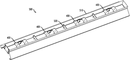
- FIGS. 5A-5C illustrate various views of an antenna array 500 , e.g. a cavity-backed slot broadband antenna.
- FIG. 5A shows a cavity-backed slot 510 and four instances of the coupling device 400 .
- the antenna array 500 includes a radome, which is omitted in this figure for illustration purposes.
- the coupling devices 400 are spaced from each other along the long axis of the cavity-backed slot 510 with an optional wall 520 , e.g. a ground plane, located at about a midpoint between adjacent coupling devices 400 .
- the wall 520 may operate to divide the slot 510 into multiple cavity-backed slots.
- the coupling devices 400 are spaced apart by a distance that is at least as large as an overall length of the coupling devices 400 .
- the distance between adjacent coupling devices is about twice the overall length of the coupling devices 400 .
- the illustrated configuration may support transmission and reception of signals in, e.g. a UHF band from about 470 MHz to about 700 MHz, or a VHF band from about 170 MHz to about 235 MHz, with relatively flat azimuthal gain, as previously described.
- an antenna array configured consistent with described embodiments are capable of providing an azimuthal gain with variation no greater than ⁇ 1.5 dB over an azimuthal angle range up to about 180°.
- the realized gain of such embodiments may depend in part on external parasitic structures, e.g. antenna tower components and/or ground planes placed to intentionally limit azimuthal angle range.
- FIG. 5B shows a top view of the antenna array 500 drawn such that the cavity-backed slot 510 is transparent, revealing feed striplines 530 behind the cavity-backed slot 510 that distribute RF power from a signal source input port 540 to each of the coupling devices 400 .
- the FIG. 5C shows a detail view of one of the coupling devices 400 , including insulating posts 550 as described earlier used to attach the coupling plates 410 to the cavity-backed slot.
- each numerical value and range should be interpreted as being approximate as if the word “about” or “approximately” preceded the value of the value or range.
- figure numbers and/or figure reference labels in the claims is intended to identify one or more possible embodiments of the claimed subject matter in order to facilitate the interpretation of the claims. Such use is not to be construed as necessarily limiting the scope of those claims to the embodiments shown in the corresponding figures.
Abstract
Description
Claims (17)
Priority Applications (1)
| Application Number | Priority Date | Filing Date | Title |
|---|---|---|---|
| US16/091,323 US10998636B2 (en) | 2016-04-05 | 2017-04-05 | Broadband cavity-backed slot antenna |
Applications Claiming Priority (3)
| Application Number | Priority Date | Filing Date | Title |
|---|---|---|---|
| US201662318661P | 2016-04-05 | 2016-04-05 | |
| US16/091,323 US10998636B2 (en) | 2016-04-05 | 2017-04-05 | Broadband cavity-backed slot antenna |
| PCT/IB2017/051961 WO2017175155A1 (en) | 2016-04-05 | 2017-04-05 | Broadband cavity-backed slot antenna |
Publications (2)
| Publication Number | Publication Date |
|---|---|
| US20190157766A1 US20190157766A1 (en) | 2019-05-23 |
| US10998636B2 true US10998636B2 (en) | 2021-05-04 |
Family
ID=60000297
Family Applications (1)
| Application Number | Title | Priority Date | Filing Date |
|---|---|---|---|
| US16/091,323 Active US10998636B2 (en) | 2016-04-05 | 2017-04-05 | Broadband cavity-backed slot antenna |
Country Status (4)
| Country | Link |
|---|---|
| US (1) | US10998636B2 (en) |
| EP (1) | EP3440739B1 (en) |
| CN (1) | CN109075452B (en) |
| WO (1) | WO2017175155A1 (en) |
Families Citing this family (1)
| Publication number | Priority date | Publication date | Assignee | Title |
|---|---|---|---|---|
| US10992049B2 (en) | 2018-02-23 | 2021-04-27 | Nokia Shanghai Bell Co., Ltd. | Elliptically polarized cavity backed wideband slot antenna |
Citations (13)
| Publication number | Priority date | Publication date | Assignee | Title |
|---|---|---|---|---|
| US3545001A (en) | 1968-04-24 | 1970-12-01 | Bendix Corp | Antenna feed comprising dipole array with conductive ground plane |
| US3750185A (en) | 1972-01-18 | 1973-07-31 | Westinghouse Electric Corp | Dipole antenna array |
| US6317099B1 (en) | 2000-01-10 | 2001-11-13 | Andrew Corporation | Folded dipole antenna |
| EP1267448A2 (en) | 2001-06-13 | 2002-12-18 | Raytheon Company | Dual-polarization common aperture antenna with longitudinal and transverse slot arrays |
| US20070080864A1 (en) | 2005-10-11 | 2007-04-12 | M/A-Com, Inc. | Broadband proximity-coupled cavity backed patch antenna |
| WO2008055526A1 (en) | 2006-11-09 | 2008-05-15 | Tes Electronic Solutions Gmbh | Antenna device, antenna system and method of operation |
| CN102117968A (en) | 2010-12-28 | 2011-07-06 | 中国兵器工业第二○六研究所 | Composite material stripline waveguide array antenna |
| US20120299790A1 (en) | 2010-02-05 | 2012-11-29 | Khamprasith Bounpraseuth | Folded-dipole flat-plate antenna |
| CN202633514U (en) | 2012-05-25 | 2012-12-26 | 四川省视频电子有限责任公司 | UHF (Ultra High Frequency) band reflection cavity dipole antenna |
| CN102842757A (en) | 2012-09-25 | 2012-12-26 | 东南大学 | Double-frequency dual-polarization cavity backed slot antenna |
| CN103904423A (en) | 2012-12-28 | 2014-07-02 | 中国航空工业第六○七研究所 | Low profile broadband medium back cavity four radiator antenna unit |
| CN104103906A (en) | 2014-08-01 | 2014-10-15 | 东南大学 | Low-cost microwave- and millimeter-wave polarized antenna of multi-layer PCB (Printed circuit board) process |
| CN104953257A (en) | 2015-05-27 | 2015-09-30 | 中国科学院电子学研究所 | Ultra-wideband radar antenna |
-
2017
- 2017-04-05 CN CN201780026599.8A patent/CN109075452B/en active Active
- 2017-04-05 US US16/091,323 patent/US10998636B2/en active Active
- 2017-04-05 WO PCT/IB2017/051961 patent/WO2017175155A1/en active Application Filing
- 2017-04-05 EP EP17778767.8A patent/EP3440739B1/en active Active
Patent Citations (13)
| Publication number | Priority date | Publication date | Assignee | Title |
|---|---|---|---|---|
| US3545001A (en) | 1968-04-24 | 1970-12-01 | Bendix Corp | Antenna feed comprising dipole array with conductive ground plane |
| US3750185A (en) | 1972-01-18 | 1973-07-31 | Westinghouse Electric Corp | Dipole antenna array |
| US6317099B1 (en) | 2000-01-10 | 2001-11-13 | Andrew Corporation | Folded dipole antenna |
| EP1267448A2 (en) | 2001-06-13 | 2002-12-18 | Raytheon Company | Dual-polarization common aperture antenna with longitudinal and transverse slot arrays |
| US20070080864A1 (en) | 2005-10-11 | 2007-04-12 | M/A-Com, Inc. | Broadband proximity-coupled cavity backed patch antenna |
| WO2008055526A1 (en) | 2006-11-09 | 2008-05-15 | Tes Electronic Solutions Gmbh | Antenna device, antenna system and method of operation |
| US20120299790A1 (en) | 2010-02-05 | 2012-11-29 | Khamprasith Bounpraseuth | Folded-dipole flat-plate antenna |
| CN102117968A (en) | 2010-12-28 | 2011-07-06 | 中国兵器工业第二○六研究所 | Composite material stripline waveguide array antenna |
| CN202633514U (en) | 2012-05-25 | 2012-12-26 | 四川省视频电子有限责任公司 | UHF (Ultra High Frequency) band reflection cavity dipole antenna |
| CN102842757A (en) | 2012-09-25 | 2012-12-26 | 东南大学 | Double-frequency dual-polarization cavity backed slot antenna |
| CN103904423A (en) | 2012-12-28 | 2014-07-02 | 中国航空工业第六○七研究所 | Low profile broadband medium back cavity four radiator antenna unit |
| CN104103906A (en) | 2014-08-01 | 2014-10-15 | 东南大学 | Low-cost microwave- and millimeter-wave polarized antenna of multi-layer PCB (Printed circuit board) process |
| CN104953257A (en) | 2015-05-27 | 2015-09-30 | 中国科学院电子学研究所 | Ultra-wideband radar antenna |
Non-Patent Citations (2)
| Title |
|---|
| Anonymous; "Cavity-Backed Slot Antennas"; Antenna-theory.com; Dec. 15, 2020; Retrieved from the Internet: URL: http://vvww.antenna-theory.com/antennas/aperture/slot2.01D [retrieved on Dec. 15, 2020]; whole document (4 pages). |
| Targonski, S.D., et al., "Design of wide-band aperture-stacked patch Microstrip Antennas", IEEE Transactions on Antennas and Propagation 46(9), Oct. 1988, abstract, 1 pg. |
Also Published As
| Publication number | Publication date |
|---|---|
| CN109075452B (en) | 2023-06-02 |
| EP3440739A1 (en) | 2019-02-13 |
| CN109075452A (en) | 2018-12-21 |
| US20190157766A1 (en) | 2019-05-23 |
| EP3440739B1 (en) | 2023-08-09 |
| EP3440739A4 (en) | 2019-12-04 |
| WO2017175155A1 (en) | 2017-10-12 |
Similar Documents
| Publication | Publication Date | Title |
|---|---|---|
| US11431087B2 (en) | Wideband, low profile, small area, circular polarized UHF antenna | |
| EP2917963B1 (en) | Dual polarization current loop radiator with integrated balun | |
| KR101435538B1 (en) | A broadband plannar Quasi-Yagi antenna | |
| US8368609B2 (en) | Omnidirectional multiple input multiple output (MIMO) antennas with polarization diversity | |
| US20170085009A1 (en) | Low-profile, broad-bandwidth, dual-polarization dipole radiating element | |
| US6278410B1 (en) | Wide frequency band planar antenna | |
| Kaboli et al. | High-isolation XX-polar antenna | |
| WO2016100291A1 (en) | Antenna systems with proximity coupled annular rectangular patches | |
| Zhou et al. | Millimeter-wave open ended SIW antenna with wide beam coverage | |
| US20140049439A1 (en) | Compact dual-polarized multiple directly fed & em coupled stepped probe element for ultra wideband performance | |
| KR101630674B1 (en) | Double dipole quasi-yagi antenna using stepped slotline structure | |
| CN115149243A (en) | Dual-frequency dual-polarization laminated patch antenna and wireless communication equipment | |
| WO2003096477A1 (en) | Broadband suspended plate antenna with multi-point feed | |
| US10998636B2 (en) | Broadband cavity-backed slot antenna | |
| US11799212B2 (en) | Collinear antenna array | |
| Demshevsky et al. | UWB antenna Vivaldi based on substrate integrated waveguide | |
| Nguyen-Trong et al. | Wideband millimeter-wave antennas with magnetic-dipole patterns integrated in metallic structures | |
| Malik et al. | Extremely close integration of dual band sub-6 GHz 4G antenna with unidirectional mm-wave 5G antenna | |
| Scorrano et al. | A novel UHF horizontally polarized omnidirectional antenna | |
| CN211045720U (en) | Horizontal polarization antenna | |
| Karthikeya et al. | Polycarbonate Based Overlapped Architecture for Landscape and Portrait Modes of mmWave 5G Smartphone | |
| Wang et al. | 60GHz stacked Yagi Magneto-Electric Dipole antenna with wideband and high gain properties | |
| Singh et al. | Comparitive Study of Return-Loss for Single and Dual Inset-Fed Microstrip Antenna | |
| Kumar et al. | Study on circular planar antenna | |
| Karamirad et al. | A very small broadband CPW-fed circular polarized antenna with two semicircles etched on ground plane |
Legal Events
| Date | Code | Title | Description |
|---|---|---|---|
| FEPP | Fee payment procedure |
Free format text: ENTITY STATUS SET TO UNDISCOUNTED (ORIGINAL EVENT CODE: BIG.); ENTITY STATUS OF PATENT OWNER: LARGE ENTITY |
|
| STPP | Information on status: patent application and granting procedure in general |
Free format text: DOCKETED NEW CASE - READY FOR EXAMINATION |
|
| STPP | Information on status: patent application and granting procedure in general |
Free format text: NON FINAL ACTION MAILED |
|
| AS | Assignment |
Owner name: NOKIA SHANGHAI BELL CO., LTD., CHINA Free format text: ASSIGNMENT OF ASSIGNORS INTEREST;ASSIGNORS:SCHEID, BENEDIKT;CAO, YAN;FARDIN, ERNEST;SIGNING DATES FROM 20191219 TO 20200106;REEL/FRAME:051571/0732 |
|
| STPP | Information on status: patent application and granting procedure in general |
Free format text: RESPONSE TO NON-FINAL OFFICE ACTION ENTERED AND FORWARDED TO EXAMINER |
|
| STPP | Information on status: patent application and granting procedure in general |
Free format text: FINAL REJECTION MAILED |
|
| STPP | Information on status: patent application and granting procedure in general |
Free format text: ADVISORY ACTION MAILED |
|
| STPP | Information on status: patent application and granting procedure in general |
Free format text: DOCKETED NEW CASE - READY FOR EXAMINATION |
|
| STPP | Information on status: patent application and granting procedure in general |
Free format text: NOTICE OF ALLOWANCE MAILED -- APPLICATION RECEIVED IN OFFICE OF PUBLICATIONS |
|
| STPP | Information on status: patent application and granting procedure in general |
Free format text: AWAITING TC RESP., ISSUE FEE NOT PAID Free format text: NOTICE OF ALLOWANCE MAILED -- APPLICATION RECEIVED IN OFFICE OF PUBLICATIONS |
|
| STPP | Information on status: patent application and granting procedure in general |
Free format text: PUBLICATIONS -- ISSUE FEE PAYMENT VERIFIED |
|
| STCF | Information on status: patent grant |
Free format text: PATENTED CASE |