US10995098B2 - Heterocyclic compound and organic light emitting device comprising the same - Google Patents
Heterocyclic compound and organic light emitting device comprising the same Download PDFInfo
- Publication number
- US10995098B2 US10995098B2 US16/313,810 US201716313810A US10995098B2 US 10995098 B2 US10995098 B2 US 10995098B2 US 201716313810 A US201716313810 A US 201716313810A US 10995098 B2 US10995098 B2 US 10995098B2
- Authority
- US
- United States
- Prior art keywords
- group
- compound
- substituted
- light emitting
- chemical formula
- Prior art date
- Legal status (The legal status is an assumption and is not a legal conclusion. Google has not performed a legal analysis and makes no representation as to the accuracy of the status listed.)
- Active, expires
Links
- 0 *C1=C(B)C([2*])=C([1*])C2=C1C1=C(O2)/C([4*])=C(/[3*])C2=C1C1=C(C=CC=C1)O2 Chemical compound *C1=C(B)C([2*])=C([1*])C2=C1C1=C(O2)/C([4*])=C(/[3*])C2=C1C1=C(C=CC=C1)O2 0.000 description 21
- JVFGMGJOYGUXIW-UHFFFAOYSA-N C1=CC2=C(C=C1)C1=C(C=C2)C2=CC=C(C3=C4\OC5=C(C=CC=C5)\C4=C4\C5=C(C=CC6=C5C=CC=C6)O\C4=C\3)C=C2N2C1=NC1=C2C=CC=C1.C1=CC=C(C2=NC(C3=CC=CC=C3)=NC(C3=CC=C(C4=C5\OC6=C(C=CC=C6)\C5=C5\C6=C(C=CC7=C6C=CC=C7)O\C5=C\4)C=C3)=N2)C=C1 Chemical compound C1=CC2=C(C=C1)C1=C(C=C2)C2=CC=C(C3=C4\OC5=C(C=CC=C5)\C4=C4\C5=C(C=CC6=C5C=CC=C6)O\C4=C\3)C=C2N2C1=NC1=C2C=CC=C1.C1=CC=C(C2=NC(C3=CC=CC=C3)=NC(C3=CC=C(C4=C5\OC6=C(C=CC=C6)\C5=C5\C6=C(C=CC7=C6C=CC=C7)O\C5=C\4)C=C3)=N2)C=C1 JVFGMGJOYGUXIW-UHFFFAOYSA-N 0.000 description 2
- DVDVARCGQXZEHV-UHFFFAOYSA-N C1=CC2=C(C=C1)C1=C(C=C2)C2=CC=C(C3=C4\OC5=C(C=CC=C5)\C4=C4\C5=C(C=CC6=C5OC5=C6C=CC=C5)O\C4=C\3)C=C2N2C1=NC1=C2C=CC=C1.C1=CC2=C(C=C1)N1C3=CC(C4=C5\OC6=C(C=CC=C6)\C5=C5\C6=C(C=CC7=C6OC6=C7C=CC=C6)O\C5=C\4)=CC=C3C3=C(C=CC=C3)C1=N2.C1=CC=C(C2=NC(C3=CC=CC=C3)=NC(C3=CC=C(C4=C5\OC6=C(C=CC=C6)\C5=C5\C6=C(C=CC7=C6OC6=C7C=CC=C6)O\C5=C\4)C=C3)=N2)C=C1 Chemical compound C1=CC2=C(C=C1)C1=C(C=C2)C2=CC=C(C3=C4\OC5=C(C=CC=C5)\C4=C4\C5=C(C=CC6=C5OC5=C6C=CC=C5)O\C4=C\3)C=C2N2C1=NC1=C2C=CC=C1.C1=CC2=C(C=C1)N1C3=CC(C4=C5\OC6=C(C=CC=C6)\C5=C5\C6=C(C=CC7=C6OC6=C7C=CC=C6)O\C5=C\4)=CC=C3C3=C(C=CC=C3)C1=N2.C1=CC=C(C2=NC(C3=CC=CC=C3)=NC(C3=CC=C(C4=C5\OC6=C(C=CC=C6)\C5=C5\C6=C(C=CC7=C6OC6=C7C=CC=C6)O\C5=C\4)C=C3)=N2)C=C1 DVDVARCGQXZEHV-UHFFFAOYSA-N 0.000 description 2
- AKBNUTNZJVLZOI-UHFFFAOYSA-N C1=CC2=C(C=C1)C1=C(C=C2)C2=CC=C(C3=C4\OC5=C(C=CC=C5)\C4=C4\C5=C(C=CC=C5)O\C4=C\3)C=C2N2C1=NC1=C2C=CC=C1.C1=CC=C(C2=NC(C3=CC=CC=C3)=NC(C3=CC=C(C4=C5\OC6=C(C=CC=C6)\C5=C5\C6=C(C=CC=C6)O\C5=C\4)C=C3)=N2)C=C1 Chemical compound C1=CC2=C(C=C1)C1=C(C=C2)C2=CC=C(C3=C4\OC5=C(C=CC=C5)\C4=C4\C5=C(C=CC=C5)O\C4=C\3)C=C2N2C1=NC1=C2C=CC=C1.C1=CC=C(C2=NC(C3=CC=CC=C3)=NC(C3=CC=C(C4=C5\OC6=C(C=CC=C6)\C5=C5\C6=C(C=CC=C6)O\C5=C\4)C=C3)=N2)C=C1 AKBNUTNZJVLZOI-UHFFFAOYSA-N 0.000 description 2
- KTOFORDXQYJFLM-UHFFFAOYSA-N C1=CC2=C(C=C1)C1=C(C=C2)C2=CC=C(C3=CC4=C(C5=C3C3=C(C=CC=C3)O5)C3=C5\C6=C(C=CC=C6)O\C5=C\C=C\3O4)C=C2N2C1=NC1=C2C=CC=C1.C1=CC2=C(C=C1)N1C3=CC(C4=CC5=C(C6=C4C4=C(C=CC=C4)O6)C4=C6\C7=C(C=CC=C7)O\C6=C\C=C\4O5)=CC=C3C3=C(C=CC=C3)C1=N2.C1=CC=C(C2=CC(C3=CC=CC=C3)=NC(C3=CC=C(C4=CC5=C(C6=C4C4=C(C=CC=C4)O6)C4=C6\C7=C(C=CC=C7)O\C6=C\C=C\4O5)C=C3)=N2)C=C1.C1=CC=C(C2=NC(C3=CC=CC=C3)=NC(C3=CC=C(C4=CC5=C(C6=C4C4=C(C=CC=C4)O6)C4=C6\C7=C(C=CC=C7)O\C6=C\C=C\4O5)C=C3)=N2)C=C1 Chemical compound C1=CC2=C(C=C1)C1=C(C=C2)C2=CC=C(C3=CC4=C(C5=C3C3=C(C=CC=C3)O5)C3=C5\C6=C(C=CC=C6)O\C5=C\C=C\3O4)C=C2N2C1=NC1=C2C=CC=C1.C1=CC2=C(C=C1)N1C3=CC(C4=CC5=C(C6=C4C4=C(C=CC=C4)O6)C4=C6\C7=C(C=CC=C7)O\C6=C\C=C\4O5)=CC=C3C3=C(C=CC=C3)C1=N2.C1=CC=C(C2=CC(C3=CC=CC=C3)=NC(C3=CC=C(C4=CC5=C(C6=C4C4=C(C=CC=C4)O6)C4=C6\C7=C(C=CC=C7)O\C6=C\C=C\4O5)C=C3)=N2)C=C1.C1=CC=C(C2=NC(C3=CC=CC=C3)=NC(C3=CC=C(C4=CC5=C(C6=C4C4=C(C=CC=C4)O6)C4=C6\C7=C(C=CC=C7)O\C6=C\C=C\4O5)C=C3)=N2)C=C1 KTOFORDXQYJFLM-UHFFFAOYSA-N 0.000 description 2
- XGGFIAWCFDZKAE-UHFFFAOYSA-N C1=CC2=C(C=C1)C1=C(C=C2)C2=CC=C(C3=CC4=C(C5=C3C=CC=C5)C3=C5\C6=C(C=CC=C6)O\C5=C\C=C\3O4)C=C2N2C1=NC1=C2C=CC=C1.C1=CC2=C(C=C1)N1C3=CC(C4=CC5=C(C6=C4C=CC=C6)C4=C6\C7=C(C=CC=C7)O\C6=C\C=C\4O5)=CC=C3C3=C(C=CC=C3)C1=N2.C1=CC=C(C2=CC(C3=CC=CC=C3)=NC(C3=CC=C(C4=CC5=C(C6=C4C=CC=C6)C4=C6\C7=C(C=CC=C7)O\C6=C\C=C\4O5)C=C3)=N2)C=C1.C1=CC=C(C2=NC(C3=CC=CC=C3)=NC(C3=CC=C(C4=CC5=C(C6=C4C=CC=C6)C4=C6\C7=C(C=CC=C7)O\C6=C\C=C\4O5)C=C3)=N2)C=C1 Chemical compound C1=CC2=C(C=C1)C1=C(C=C2)C2=CC=C(C3=CC4=C(C5=C3C=CC=C5)C3=C5\C6=C(C=CC=C6)O\C5=C\C=C\3O4)C=C2N2C1=NC1=C2C=CC=C1.C1=CC2=C(C=C1)N1C3=CC(C4=CC5=C(C6=C4C=CC=C6)C4=C6\C7=C(C=CC=C7)O\C6=C\C=C\4O5)=CC=C3C3=C(C=CC=C3)C1=N2.C1=CC=C(C2=CC(C3=CC=CC=C3)=NC(C3=CC=C(C4=CC5=C(C6=C4C=CC=C6)C4=C6\C7=C(C=CC=C7)O\C6=C\C=C\4O5)C=C3)=N2)C=C1.C1=CC=C(C2=NC(C3=CC=CC=C3)=NC(C3=CC=C(C4=CC5=C(C6=C4C=CC=C6)C4=C6\C7=C(C=CC=C7)O\C6=C\C=C\4O5)C=C3)=N2)C=C1 XGGFIAWCFDZKAE-UHFFFAOYSA-N 0.000 description 2
- ZAFUOKPOQHKDQW-UHFFFAOYSA-N C1=CC2=C(C=C1)C1=C(C=C2)C2=CC=C(C3=CC4=C(C=C3)C3=C5\C6=C(C=CC=C6)O\C5=C\C=C\3O4)C=C2N2C1=NC1=C2C=CC=C1.C1=CC=C(C2=NC(C3=CC=CC=C3)=NC(C3=CC=C(C4=CC5=C(C=C4)C4=C6\C7=C(C=CC=C7)O\C6=C\C=C\4O5)C=C3)=N2)C=C1 Chemical compound C1=CC2=C(C=C1)C1=C(C=C2)C2=CC=C(C3=CC4=C(C=C3)C3=C5\C6=C(C=CC=C6)O\C5=C\C=C\3O4)C=C2N2C1=NC1=C2C=CC=C1.C1=CC=C(C2=NC(C3=CC=CC=C3)=NC(C3=CC=C(C4=CC5=C(C=C4)C4=C6\C7=C(C=CC=C7)O\C6=C\C=C\4O5)C=C3)=N2)C=C1 ZAFUOKPOQHKDQW-UHFFFAOYSA-N 0.000 description 2
- HKTHYVQMMBHBKP-UHFFFAOYSA-N C1=CC2=C(C=C1)C1=C(C=C2)C2=CC=C(C3=CC=C(C4=C5\OC6=C(C=CC=C6)\C5=C5\C6=C(C=CC7=C6C=CC=C7)O\C5=C\4)C=C3)C=C2N2C1=NC1=C2C=CC=C1.C1=CC2=C(C=C1)C1=C(C=C2)O/C2=C/C(C3=CC=C(C4=CC=C5C(=C4)N4C(=NC6=C4C=CC=C6)C4=C5C=CC=C4)C=C3)=C3/OC4=C(C=CC=C4)/C3=C\12.C1=CC=C(C2=CC=C(C3=C4\OC5=C(C=CC=C5)\C4=C4\C5=C(C=CC6=C5C=CC=C6)O\C4=C\3)C=C2)N=C1 Chemical compound C1=CC2=C(C=C1)C1=C(C=C2)C2=CC=C(C3=CC=C(C4=C5\OC6=C(C=CC=C6)\C5=C5\C6=C(C=CC7=C6C=CC=C7)O\C5=C\4)C=C3)C=C2N2C1=NC1=C2C=CC=C1.C1=CC2=C(C=C1)C1=C(C=C2)O/C2=C/C(C3=CC=C(C4=CC=C5C(=C4)N4C(=NC6=C4C=CC=C6)C4=C5C=CC=C4)C=C3)=C3/OC4=C(C=CC=C4)/C3=C\12.C1=CC=C(C2=CC=C(C3=C4\OC5=C(C=CC=C5)\C4=C4\C5=C(C=CC6=C5C=CC=C6)O\C4=C\3)C=C2)N=C1 HKTHYVQMMBHBKP-UHFFFAOYSA-N 0.000 description 2
- ZYNDGNZKMUCKSX-UHFFFAOYSA-N C1=CC2=C(C=C1)C1=C(C=C2)C2=CC=C(C3=CC=C(C4=C5\OC6=C(C=CC=C6)\C5=C5\C6=C(C=CC7=C6OC6=C7C=CC=C6)O\C5=C\4)C=C3)C=C2N2C1=NC1=C2C=CC=C1.C1=CC2=C(C=C1)N1C3=CC(C4=CC=C(C5=C6\OC7=C(C=CC=C7)\C6=C6\C7=C(C=CC8=C7OC7=C8C=CC=C7)O\C6=C\5)C=C4)=CC=C3C3=C(C=CC=C3)C1=N2.C1=CC=C(C2=CC(C3=CC=C(C4=C5\OC6=C(C=CC=C6)\C5=C5\C6=C(C=CC7=C6OC6=C7C=CC=C6)O\C5=C\4)C=C3)=CC(C3=CC=CC=C3)=N2)C=C1 Chemical compound C1=CC2=C(C=C1)C1=C(C=C2)C2=CC=C(C3=CC=C(C4=C5\OC6=C(C=CC=C6)\C5=C5\C6=C(C=CC7=C6OC6=C7C=CC=C6)O\C5=C\4)C=C3)C=C2N2C1=NC1=C2C=CC=C1.C1=CC2=C(C=C1)N1C3=CC(C4=CC=C(C5=C6\OC7=C(C=CC=C7)\C6=C6\C7=C(C=CC8=C7OC7=C8C=CC=C7)O\C6=C\5)C=C4)=CC=C3C3=C(C=CC=C3)C1=N2.C1=CC=C(C2=CC(C3=CC=C(C4=C5\OC6=C(C=CC=C6)\C5=C5\C6=C(C=CC7=C6OC6=C7C=CC=C6)O\C5=C\4)C=C3)=CC(C3=CC=CC=C3)=N2)C=C1 ZYNDGNZKMUCKSX-UHFFFAOYSA-N 0.000 description 2
- DBAAPPAENOKTDM-UHFFFAOYSA-N C1=CC2=C(C=C1)C1=C(C=C2)C2=CC=C(C3=CC=C(C4=C5\OC6=C(C=CC=C6)\C5=C5\C6=C(C=CC=C6)O\C5=C\4)C=C3)C=C2N2C1=NC1=C2C=CC=C1.C1=CC2=C(C=C1)N1C3=CC(C4=CC=C(C5=C6\OC7=C(C=CC=C7)\C6=C6\C7=C(C=CC=C7)O\C6=C\5)C=C4)=CC=C3C3=C(C=CC=C3)C1=N2.C1=CC=C(C2=CC=C(C3=C4\OC5=C(C=CC=C5)\C4=C4\C5=C(C=CC=C5)O\C4=C\3)C=C2)N=C1 Chemical compound C1=CC2=C(C=C1)C1=C(C=C2)C2=CC=C(C3=CC=C(C4=C5\OC6=C(C=CC=C6)\C5=C5\C6=C(C=CC=C6)O\C5=C\4)C=C3)C=C2N2C1=NC1=C2C=CC=C1.C1=CC2=C(C=C1)N1C3=CC(C4=CC=C(C5=C6\OC7=C(C=CC=C7)\C6=C6\C7=C(C=CC=C7)O\C6=C\5)C=C4)=CC=C3C3=C(C=CC=C3)C1=N2.C1=CC=C(C2=CC=C(C3=C4\OC5=C(C=CC=C5)\C4=C4\C5=C(C=CC=C5)O\C4=C\3)C=C2)N=C1 DBAAPPAENOKTDM-UHFFFAOYSA-N 0.000 description 2
- UAJWMYSTACHVQF-UHFFFAOYSA-N C1=CC2=C(C=C1)C1=C(C=C2)C2=CC=C(C3=CC=C(C4=CC5=C(C6=C4C4=C(C=CC=C4)O6)C4=C6\C7=C(C=CC=C7)O\C6=C\C=C\4O5)C=C3)C=C2N2C1=NC1=C2C=CC=C1.C1=CC2=C(C=C1)N1C3=CC(C4=CC=C(C5=CC6=C(C7=C5C5=C(C=CC=C5)O7)C5=C7\C8=C(C=CC=C8)O\C7=C\C=C\5O6)C=C4)=CC=C3C3=C(C=CC=C3)C1=N2.C1=CC=C(C2=CC(C3=CC=C(C4=CC5=C(C6=C4C4=C(C=CC=C4)O6)C4=C6\C7=C(C=CC=C7)O\C6=C\C=C\4O5)C=C3)=CC(C3=CC=CC=C3)=N2)C=C1.C1=CC=C(C2=CC=C(C3=CC4=C(C5=C3C3=C(C=CC=C3)O5)C3=C5\C6=C(C=CC=C6)O\C5=C\C=C\3O4)C=C2)N=C1 Chemical compound C1=CC2=C(C=C1)C1=C(C=C2)C2=CC=C(C3=CC=C(C4=CC5=C(C6=C4C4=C(C=CC=C4)O6)C4=C6\C7=C(C=CC=C7)O\C6=C\C=C\4O5)C=C3)C=C2N2C1=NC1=C2C=CC=C1.C1=CC2=C(C=C1)N1C3=CC(C4=CC=C(C5=CC6=C(C7=C5C5=C(C=CC=C5)O7)C5=C7\C8=C(C=CC=C8)O\C7=C\C=C\5O6)C=C4)=CC=C3C3=C(C=CC=C3)C1=N2.C1=CC=C(C2=CC(C3=CC=C(C4=CC5=C(C6=C4C4=C(C=CC=C4)O6)C4=C6\C7=C(C=CC=C7)O\C6=C\C=C\4O5)C=C3)=CC(C3=CC=CC=C3)=N2)C=C1.C1=CC=C(C2=CC=C(C3=CC4=C(C5=C3C3=C(C=CC=C3)O5)C3=C5\C6=C(C=CC=C6)O\C5=C\C=C\3O4)C=C2)N=C1 UAJWMYSTACHVQF-UHFFFAOYSA-N 0.000 description 2
- RMSLXQLKRWVKDH-UHFFFAOYSA-N C1=CC2=C(C=C1)C1=C(C=C2)C2=CC=C(C3=CC=C(C4=CC5=C(C6=C4C=CC=C6)C4=C6\C7=C(C=CC=C7)O\C6=C\C=C\4O5)C=C3)C=C2N2C1=NC1=C2C=CC=C1.C1=CC2=C(C=C1)N1C3=CC(C4=CC=C(C5=CC6=C(C7=C5C=CC=C7)C5=C7\C8=C(C=CC=C8)O\C7=C\C=C\5O6)C=C4)=CC=C3C3=C(C=CC=C3)C1=N2.C1=CC=C(C2=CC(C3=CC=C(C4=CC5=C(C6=C4C=CC=C6)C4=C6\C7=C(C=CC=C7)O\C6=C\C=C\4O5)C=C3)=CC(C3=CC=CC=C3)=N2)C=C1.C1=CC=C(C2=CC=C(C3=CC4=C(C5=C3C=CC=C5)C3=C5\C6=C(C=CC=C6)O\C5=C\C=C\3O4)C=C2)N=C1 Chemical compound C1=CC2=C(C=C1)C1=C(C=C2)C2=CC=C(C3=CC=C(C4=CC5=C(C6=C4C=CC=C6)C4=C6\C7=C(C=CC=C7)O\C6=C\C=C\4O5)C=C3)C=C2N2C1=NC1=C2C=CC=C1.C1=CC2=C(C=C1)N1C3=CC(C4=CC=C(C5=CC6=C(C7=C5C=CC=C7)C5=C7\C8=C(C=CC=C8)O\C7=C\C=C\5O6)C=C4)=CC=C3C3=C(C=CC=C3)C1=N2.C1=CC=C(C2=CC(C3=CC=C(C4=CC5=C(C6=C4C=CC=C6)C4=C6\C7=C(C=CC=C7)O\C6=C\C=C\4O5)C=C3)=CC(C3=CC=CC=C3)=N2)C=C1.C1=CC=C(C2=CC=C(C3=CC4=C(C5=C3C=CC=C5)C3=C5\C6=C(C=CC=C6)O\C5=C\C=C\3O4)C=C2)N=C1 RMSLXQLKRWVKDH-UHFFFAOYSA-N 0.000 description 2
- TXRLTKBLHDRJAE-UHFFFAOYSA-N C1=CC2=C(C=C1)C1=C(C=C2)C2=CC=C(C3=CC=C(C4=CC5=C(C=C4)C4=C6\C7=C(C=CC=C7)O\C6=C\C=C\4O5)C=C3)C=C2N2C1=NC1=C2C=CC=C1.C1=CC2=C(C=C1)N1C3=CC(C4=CC=C(C5=CC6=C(C=C5)C5=C7\C8=C(C=CC=C8)O\C7=C\C=C\5O6)C=C4)=CC=C3C3=C(C=CC=C3)C1=N2.C1=CC=C(C2=CC=C(C3=CC4=C(C=C3)C3=C5\C6=C(C=CC=C6)O\C5=C\C=C\3O4)C=C2)N=C1 Chemical compound C1=CC2=C(C=C1)C1=C(C=C2)C2=CC=C(C3=CC=C(C4=CC5=C(C=C4)C4=C6\C7=C(C=CC=C7)O\C6=C\C=C\4O5)C=C3)C=C2N2C1=NC1=C2C=CC=C1.C1=CC2=C(C=C1)N1C3=CC(C4=CC=C(C5=CC6=C(C=C5)C5=C7\C8=C(C=CC=C8)O\C7=C\C=C\5O6)C=C4)=CC=C3C3=C(C=CC=C3)C1=N2.C1=CC=C(C2=CC=C(C3=CC4=C(C=C3)C3=C5\C6=C(C=CC=C6)O\C5=C\C=C\3O4)C=C2)N=C1 TXRLTKBLHDRJAE-UHFFFAOYSA-N 0.000 description 2
- WFWNQIDUNRQWCM-UHFFFAOYSA-N C1=CC2=C(C=C1)C1=C(C=C2)O/C2=C/C(C3=CC=C(C4=CC=NC=C4)C=C3)=C3/OC4=C(C=CC=C4)/C3=C\12.C1=CN=CC(C2=CC=C(C3=C4\OC5=C(C=CC=C5)\C4=C4\C5=C(C=CC6=C5C=CC=C6)O\C4=C\3)C=C2)=C1 Chemical compound C1=CC2=C(C=C1)C1=C(C=C2)O/C2=C/C(C3=CC=C(C4=CC=NC=C4)C=C3)=C3/OC4=C(C=CC=C4)/C3=C\12.C1=CN=CC(C2=CC=C(C3=C4\OC5=C(C=CC=C5)\C4=C4\C5=C(C=CC6=C5C=CC=C6)O\C4=C\3)C=C2)=C1 WFWNQIDUNRQWCM-UHFFFAOYSA-N 0.000 description 2
- MJOHGUBSEBQYJD-UHFFFAOYSA-N C1=CC2=C(C=C1)C1=C(C=C2)O/C2=C/C(C3=CC=C4C(=C3)N3C(=NC5=C3C=CC=C5)C3=C4C=CC=C3)=C3/OC4=C(C=CC=C4)/C3=C\12.C1=CC2=C(C=C1)C1=C(C=C2)O/C2=C/C(C3=CC=NC=C3)=C3/OC4=C(C=CC=C4)/C3=C\12.C1=CC=C(C2=C3\OC4=C(C=CC=C4)\C3=C3\C4=C(C=CC5=C4C=CC=C5)O\C3=C\2)N=C1.C1=CN=CC(C2=C3\OC4=C(C=CC=C4)\C3=C3\C4=C(C=CC5=C4C=CC=C5)O\C3=C\2)=C1.O=P(C1=CC=CC=C1)(C1=CC=CC=C1)C1=C2\OC3=C(C=CC=C3)\C2=C2\C3=C(C=CC4=C3C=CC=C4)O\C2=C\1 Chemical compound C1=CC2=C(C=C1)C1=C(C=C2)O/C2=C/C(C3=CC=C4C(=C3)N3C(=NC5=C3C=CC=C5)C3=C4C=CC=C3)=C3/OC4=C(C=CC=C4)/C3=C\12.C1=CC2=C(C=C1)C1=C(C=C2)O/C2=C/C(C3=CC=NC=C3)=C3/OC4=C(C=CC=C4)/C3=C\12.C1=CC=C(C2=C3\OC4=C(C=CC=C4)\C3=C3\C4=C(C=CC5=C4C=CC=C5)O\C3=C\2)N=C1.C1=CN=CC(C2=C3\OC4=C(C=CC=C4)\C3=C3\C4=C(C=CC5=C4C=CC=C5)O\C3=C\2)=C1.O=P(C1=CC=CC=C1)(C1=CC=CC=C1)C1=C2\OC3=C(C=CC=C3)\C2=C2\C3=C(C=CC4=C3C=CC=C4)O\C2=C\1 MJOHGUBSEBQYJD-UHFFFAOYSA-N 0.000 description 2
- YFNWNXWAPMMHEJ-UHFFFAOYSA-N C1=CC2=C(C=C1)C1=C(O2)C2=C(C=C1)O/C1=C/C(C3=CC=C(C4=CC=NC=C4)C=C3)=C3/OC4=C(C=CC=C4)/C3=C\21.C1=CC=C(C2=CC=C(C3=C4\OC5=C(C=CC=C5)\C4=C4\C5=C(C=CC6=C5OC5=C6C=CC=C5)O\C4=C\3)C=C2)N=C1.C1=CC=C(N(C2=CC=CC=C2)C2=CC3=C(C=C2)C2=C4/C5=C(C=CC=C5)O/C4=C(N(C4=CC=CC=C4)C4=CC=CC=C4)/C=C\2O3)C=C1.C1=CN=CC(C2=CC=C(C3=C4\OC5=C(C=CC=C5)\C4=C4\C5=C(C=CC6=C5OC5=C6C=CC=C5)O\C4=C\3)C=C2)=C1 Chemical compound C1=CC2=C(C=C1)C1=C(O2)C2=C(C=C1)O/C1=C/C(C3=CC=C(C4=CC=NC=C4)C=C3)=C3/OC4=C(C=CC=C4)/C3=C\21.C1=CC=C(C2=CC=C(C3=C4\OC5=C(C=CC=C5)\C4=C4\C5=C(C=CC6=C5OC5=C6C=CC=C5)O\C4=C\3)C=C2)N=C1.C1=CC=C(N(C2=CC=CC=C2)C2=CC3=C(C=C2)C2=C4/C5=C(C=CC=C5)O/C4=C(N(C4=CC=CC=C4)C4=CC=CC=C4)/C=C\2O3)C=C1.C1=CN=CC(C2=CC=C(C3=C4\OC5=C(C=CC=C5)\C4=C4\C5=C(C=CC6=C5OC5=C6C=CC=C5)O\C4=C\3)C=C2)=C1 YFNWNXWAPMMHEJ-UHFFFAOYSA-N 0.000 description 2
- PYBNWSROKVYWQR-UHFFFAOYSA-N C1=CC2=C(C=C1)C1=C(O2)C2=C(C=C1)O/C1=C/C(C3=CC=NC=C3)=C3/OC4=C(C=CC=C4)/C3=C\21.C1=CC=C(C2=C3\OC4=C(C=CC=C4)\C3=C3\C4=C(C=CC5=C4OC4=C5C=CC=C4)O\C3=C\2)N=C1.C1=CN=CC(C2=C3\OC4=C(C=CC=C4)\C3=C3\C4=C(C=CC5=C4OC4=C5C=CC=C4)O\C3=C\2)=C1.O=P(C1=CC=CC=C1)(C1=CC=CC=C1)C1=C2\OC3=C(C=CC=C3)\C2=C2\C3=C(C=CC4=C3OC3=C4C=CC=C3)O\C2=C\1 Chemical compound C1=CC2=C(C=C1)C1=C(O2)C2=C(C=C1)O/C1=C/C(C3=CC=NC=C3)=C3/OC4=C(C=CC=C4)/C3=C\21.C1=CC=C(C2=C3\OC4=C(C=CC=C4)\C3=C3\C4=C(C=CC5=C4OC4=C5C=CC=C4)O\C3=C\2)N=C1.C1=CN=CC(C2=C3\OC4=C(C=CC=C4)\C3=C3\C4=C(C=CC5=C4OC4=C5C=CC=C4)O\C3=C\2)=C1.O=P(C1=CC=CC=C1)(C1=CC=CC=C1)C1=C2\OC3=C(C=CC=C3)\C2=C2\C3=C(C=CC4=C3OC3=C4C=CC=C3)O\C2=C\1 PYBNWSROKVYWQR-UHFFFAOYSA-N 0.000 description 2
- BBKGIXDUZBQZHZ-UHFFFAOYSA-N C1=CC2=C(C=C1)C1=C(O2)C2=C(C=C1C1=CC=C(C3=CC=NC=C3)C=C1)O/C1=C\C=C3\OC4=C(C=CC=C4)\C3=C\21.C1=CN=CC(C2=CC=C(C3=CC4=C(C5=C3C3=C(C=CC=C3)O5)C3=C5\C6=C(C=CC=C6)O\C5=C\C=C\3O4)C=C2)=C1 Chemical compound C1=CC2=C(C=C1)C1=C(O2)C2=C(C=C1C1=CC=C(C3=CC=NC=C3)C=C1)O/C1=C\C=C3\OC4=C(C=CC=C4)\C3=C\21.C1=CN=CC(C2=CC=C(C3=CC4=C(C5=C3C3=C(C=CC=C3)O5)C3=C5\C6=C(C=CC=C6)O\C5=C\C=C\3O4)C=C2)=C1 BBKGIXDUZBQZHZ-UHFFFAOYSA-N 0.000 description 2
- LNUSYGPNEODMFO-UHFFFAOYSA-N C1=CC2=C(C=C1)C1=C(O2)C2=C(C=C1C1=CC=NC=C1)O/C1=C\C=C3\OC4=C(C=CC=C4)\C3=C\21.C1=CC=C(C2=CC3=C(C4=C2C2=C(C=CC=C2)O4)C2=C4\C5=C(C=CC=C5)O\C4=C\C=C\2O3)N=C1.C1=CN=CC(C2=CC3=C(C4=C2C2=C(C=CC=C2)O4)C2=C4\C5=C(C=CC=C5)O\C4=C\C=C\2O3)=C1 Chemical compound C1=CC2=C(C=C1)C1=C(O2)C2=C(C=C1C1=CC=NC=C1)O/C1=C\C=C3\OC4=C(C=CC=C4)\C3=C\21.C1=CC=C(C2=CC3=C(C4=C2C2=C(C=CC=C2)O4)C2=C4\C5=C(C=CC=C5)O\C4=C\C=C\2O3)N=C1.C1=CN=CC(C2=CC3=C(C4=C2C2=C(C=CC=C2)O4)C2=C4\C5=C(C=CC=C5)O\C4=C\C=C\2O3)=C1 LNUSYGPNEODMFO-UHFFFAOYSA-N 0.000 description 2
- GBSDMLZFNSNULP-UHFFFAOYSA-N C1=CC2=C(C=C1)C1=C3/C4=C(C=CC=C4)O/C3=C/C(C3=CC=C(C4=CC=NC=C4)C=C3)=C\1O2.C1=CN=CC(C2=CC=C(C3=C4\OC5=C(C=CC=C5)\C4=C4\C5=C(C=CC=C5)O\C4=C\3)C=C2)=C1 Chemical compound C1=CC2=C(C=C1)C1=C3/C4=C(C=CC=C4)O/C3=C/C(C3=CC=C(C4=CC=NC=C4)C=C3)=C\1O2.C1=CN=CC(C2=CC=C(C3=C4\OC5=C(C=CC=C5)\C4=C4\C5=C(C=CC=C5)O\C4=C\3)C=C2)=C1 GBSDMLZFNSNULP-UHFFFAOYSA-N 0.000 description 2
- SWCRONWQQWFIHW-UHFFFAOYSA-N C1=CC2=C(C=C1)C1=C3/C4=C(C=CC=C4)O/C3=C/C(C3=CC=NC=C3)=C\1O2.C1=CC2=C(C=C1)N1C3=CC(C4=C5\OC6=C(C=CC=C6)\C5=C5\C6=C(C=CC=C6)O\C5=C\4)=CC=C3C3=C(C=CC=C3)C1=N2.C1=CC=C(C2=C3\OC4=C(C=CC=C4)\C3=C3\C4=C(C=CC=C4)O\C3=C\2)N=C1.C1=CN=CC(C2=C3\OC4=C(C=CC=C4)\C3=C3\C4=C(C=CC=C4)O\C3=C\2)=C1.O=P(C1=CC=CC=C1)(C1=CC=CC=C1)C1=C2\OC3=C(C=CC=C3)\C2=C2\C3=C(C=CC=C3)O\C2=C\1 Chemical compound C1=CC2=C(C=C1)C1=C3/C4=C(C=CC=C4)O/C3=C/C(C3=CC=NC=C3)=C\1O2.C1=CC2=C(C=C1)N1C3=CC(C4=C5\OC6=C(C=CC=C6)\C5=C5\C6=C(C=CC=C6)O\C5=C\4)=CC=C3C3=C(C=CC=C3)C1=N2.C1=CC=C(C2=C3\OC4=C(C=CC=C4)\C3=C3\C4=C(C=CC=C4)O\C3=C\2)N=C1.C1=CN=CC(C2=C3\OC4=C(C=CC=C4)\C3=C3\C4=C(C=CC=C4)O\C3=C\2)=C1.O=P(C1=CC=CC=C1)(C1=CC=CC=C1)C1=C2\OC3=C(C=CC=C3)\C2=C2\C3=C(C=CC=C3)O\C2=C\1 SWCRONWQQWFIHW-UHFFFAOYSA-N 0.000 description 2
- AHYBCYAZROXGFB-UHFFFAOYSA-N C1=CC2=C(C=C1)C1=C3\C4=C(C=C(C5=CC=C(C6=CC=NC=C6)C=C5)C5=C4C=CC=C5)O\C3=C/C=C\1O2.C1=CN=CC(C2=CC=C(C3=CC4=C(C5=C3C=CC=C5)C3=C5\C6=C(C=CC=C6)O\C5=C\C=C\3O4)C=C2)=C1 Chemical compound C1=CC2=C(C=C1)C1=C3\C4=C(C=C(C5=CC=C(C6=CC=NC=C6)C=C5)C5=C4C=CC=C5)O\C3=C/C=C\1O2.C1=CN=CC(C2=CC=C(C3=CC4=C(C5=C3C=CC=C5)C3=C5\C6=C(C=CC=C6)O\C5=C\C=C\3O4)C=C2)=C1 AHYBCYAZROXGFB-UHFFFAOYSA-N 0.000 description 2
- ALWLRVJLRWYCAP-UHFFFAOYSA-N C1=CC2=C(C=C1)C1=C3\C4=C(C=C(C5=CC=C(C6=CC=NC=C6)C=C5)C=C4)O\C3=C/C=C\1O2.C1=CN=CC(C2=CC=C(C3=CC4=C(C=C3)C3=C5\C6=C(C=CC=C6)O\C5=C\C=C\3O4)C=C2)=C1 Chemical compound C1=CC2=C(C=C1)C1=C3\C4=C(C=C(C5=CC=C(C6=CC=NC=C6)C=C5)C=C4)O\C3=C/C=C\1O2.C1=CN=CC(C2=CC=C(C3=CC4=C(C=C3)C3=C5\C6=C(C=CC=C6)O\C5=C\C=C\3O4)C=C2)=C1 ALWLRVJLRWYCAP-UHFFFAOYSA-N 0.000 description 2
- HFWHAYFPBKGOFZ-UHFFFAOYSA-N C1=CC2=C(C=C1)C1=C3\C4=C(C=C(C5=CC=NC=C5)C5=C4C=CC=C5)O\C3=C/C=C\1O2.C1=CN=CC(C2=CC3=C(C4=C2C=CC=C4)C2=C4\C5=C(C=CC=C5)O\C4=C\C=C\2O3)=C1 Chemical compound C1=CC2=C(C=C1)C1=C3\C4=C(C=C(C5=CC=NC=C5)C5=C4C=CC=C5)O\C3=C/C=C\1O2.C1=CN=CC(C2=CC3=C(C4=C2C=CC=C4)C2=C4\C5=C(C=CC=C5)O\C4=C\C=C\2O3)=C1 HFWHAYFPBKGOFZ-UHFFFAOYSA-N 0.000 description 2
- KUXOBSDTDQUYHU-UHFFFAOYSA-N C1=CC2=C(C=C1)C1=C3\C4=C(C=C(C5=CC=NC=C5)C=C4)O\C3=C/C=C\1O2.C1=CC2=C(C=C1)N1C3=CC(C4=CC5=C(C=C4)C4=C6\C7=C(C=CC=C7)O\C6=C\C=C\4O5)=CC=C3C3=C(C=CC=C3)C1=N2.C1=CC=C(C2=CC3=C(C=C2)C2=C4\C5=C(C=CC=C5)O\C4=C\C=C\2O3)N=C1.C1=CN=CC(C2=CC3=C(C=C2)C2=C4\C5=C(C=CC=C5)O\C4=C\C=C\2O3)=C1.O=P(C1=CC=CC=C1)(C1=CC=CC=C1)C1=CC2=C(C=C1)C1=C3\C4=C(C=CC=C4)O\C3=C\C=C\1O2 Chemical compound C1=CC2=C(C=C1)C1=C3\C4=C(C=C(C5=CC=NC=C5)C=C4)O\C3=C/C=C\1O2.C1=CC2=C(C=C1)N1C3=CC(C4=CC5=C(C=C4)C4=C6\C7=C(C=CC=C7)O\C6=C\C=C\4O5)=CC=C3C3=C(C=CC=C3)C1=N2.C1=CC=C(C2=CC3=C(C=C2)C2=C4\C5=C(C=CC=C5)O\C4=C\C=C\2O3)N=C1.C1=CN=CC(C2=CC3=C(C=C2)C2=C4\C5=C(C=CC=C5)O\C4=C\C=C\2O3)=C1.O=P(C1=CC=CC=C1)(C1=CC=CC=C1)C1=CC2=C(C=C1)C1=C3\C4=C(C=CC=C4)O\C3=C\C=C\1O2 KUXOBSDTDQUYHU-UHFFFAOYSA-N 0.000 description 2
- SAJABXROWOOJAK-UHFFFAOYSA-N C1=CC=C(C2=CC(C3=C4\OC5=C(C=CC=C5)\C4=C4\C5=C(C=CC6=C5C=CC=C6)O\C4=C\3)=CC(C3=CC=CC=C3)=N2)C=C1.O=P(C1=CC=CC=C1)(C1=CC=CC=C1)C1=CC=C(C2=C3\OC4=C(C=CC=C4)\C3=C3\C4=C(C=CC5=C4C=CC=C5)O\C3=C\2)C=C1 Chemical compound C1=CC=C(C2=CC(C3=C4\OC5=C(C=CC=C5)\C4=C4\C5=C(C=CC6=C5C=CC=C6)O\C4=C\3)=CC(C3=CC=CC=C3)=N2)C=C1.O=P(C1=CC=CC=C1)(C1=CC=CC=C1)C1=CC=C(C2=C3\OC4=C(C=CC=C4)\C3=C3\C4=C(C=CC5=C4C=CC=C5)O\C3=C\2)C=C1 SAJABXROWOOJAK-UHFFFAOYSA-N 0.000 description 2
- XTZFXGXMDGPDIB-UHFFFAOYSA-N C1=CC=C(C2=CC(C3=C4\OC5=C(C=CC=C5)\C4=C4\C5=C(C=CC6=C5OC5=C6C=CC=C5)O\C4=C\3)=CC(C3=CC=CC=C3)=N2)C=C1.O=P(C1=CC=CC=C1)(C1=CC=CC=C1)C1=CC=C(C2=C3\OC4=C(C=CC=C4)\C3=C3\C4=C(C=CC5=C4OC4=C5C=CC=C4)O\C3=C\2)C=C1 Chemical compound C1=CC=C(C2=CC(C3=C4\OC5=C(C=CC=C5)\C4=C4\C5=C(C=CC6=C5OC5=C6C=CC=C5)O\C4=C\3)=CC(C3=CC=CC=C3)=N2)C=C1.O=P(C1=CC=CC=C1)(C1=CC=CC=C1)C1=CC=C(C2=C3\OC4=C(C=CC=C4)\C3=C3\C4=C(C=CC5=C4OC4=C5C=CC=C4)O\C3=C\2)C=C1 XTZFXGXMDGPDIB-UHFFFAOYSA-N 0.000 description 2
- SNBOGSUMRFLSIN-UHFFFAOYSA-N C1=CC=C(C2=CC(C3=C4\OC5=C(C=CC=C5)\C4=C4\C5=C(C=CC=C5)O\C4=C\3)=CC(C3=CC=CC=C3)=N2)C=C1.O=P(C1=CC=CC=C1)(C1=CC=CC=C1)C1=CC=C(C2=C3\OC4=C(C=CC=C4)\C3=C3\C4=C(C=CC=C4)O\C3=C\2)C=C1 Chemical compound C1=CC=C(C2=CC(C3=C4\OC5=C(C=CC=C5)\C4=C4\C5=C(C=CC=C5)O\C4=C\3)=CC(C3=CC=CC=C3)=N2)C=C1.O=P(C1=CC=CC=C1)(C1=CC=CC=C1)C1=CC=C(C2=C3\OC4=C(C=CC=C4)\C3=C3\C4=C(C=CC=C4)O\C3=C\2)C=C1 SNBOGSUMRFLSIN-UHFFFAOYSA-N 0.000 description 2
- FMGAJKYDMVLPQM-UHFFFAOYSA-N C1=CC=C(C2=CC(C3=CC4=C(C5=C3C3=C(C=CC=C3)O5)C3=C5\C6=C(C=CC=C6)O\C5=C\C=C\3O4)=CC(C3=CC=CC=C3)=N2)C=C1.C1=CC=C(C2=CC(C3=CC=CC=C3)=NC(C3=CC4=C(C5=C3C3=C(C=CC=C3)O5)C3=C5\C6=C(C=CC=C6)O\C5=C\C=C\3O4)=C2)C=C1.O=P(C1=CC=CC=C1)(C1=CC=CC=C1)C1=CC2=C(C3=C1C1=C(C=CC=C1)O3)C1=C3\C4=C(C=CC=C4)O\C3=C\C=C\1O2.O=P(C1=CC=CC=C1)(C1=CC=CC=C1)C1=CC=C(C2=CC3=C(C4=C2C2=C(C=CC=C2)O4)C2=C4\C5=C(C=CC=C5)O\C4=C\C=C\2O3)C=C1 Chemical compound C1=CC=C(C2=CC(C3=CC4=C(C5=C3C3=C(C=CC=C3)O5)C3=C5\C6=C(C=CC=C6)O\C5=C\C=C\3O4)=CC(C3=CC=CC=C3)=N2)C=C1.C1=CC=C(C2=CC(C3=CC=CC=C3)=NC(C3=CC4=C(C5=C3C3=C(C=CC=C3)O5)C3=C5\C6=C(C=CC=C6)O\C5=C\C=C\3O4)=C2)C=C1.O=P(C1=CC=CC=C1)(C1=CC=CC=C1)C1=CC2=C(C3=C1C1=C(C=CC=C1)O3)C1=C3\C4=C(C=CC=C4)O\C3=C\C=C\1O2.O=P(C1=CC=CC=C1)(C1=CC=CC=C1)C1=CC=C(C2=CC3=C(C4=C2C2=C(C=CC=C2)O4)C2=C4\C5=C(C=CC=C5)O\C4=C\C=C\2O3)C=C1 FMGAJKYDMVLPQM-UHFFFAOYSA-N 0.000 description 2
- QVHWGIMRRQYBLX-UHFFFAOYSA-N C1=CC=C(C2=CC(C3=CC4=C(C5=C3C=CC=C5)C3=C5\C6=C(C=CC=C6)O\C5=C\C=C\3O4)=CC(C3=CC=CC=C3)=N2)C=C1.C1=CC=C(C2=CC(C3=CC=CC=C3)=NC(C3=CC4=C(C5=C3C=CC=C5)C3=C5\C6=C(C=CC=C6)O\C5=C\C=C\3O4)=C2)C=C1.C1=CC=C(C2=CC3=C(C4=C2C=CC=C4)C2=C4\C5=C(C=CC=C5)O\C4=C\C=C\2O3)N=C1.O=P(C1=CC=CC=C1)(C1=CC=CC=C1)C1=CC2=C(C3=C1C=CC=C3)C1=C3\C4=C(C=CC=C4)O\C3=C\C=C\1O2.O=P(C1=CC=CC=C1)(C1=CC=CC=C1)C1=CC=C(C2=CC3=C(C4=C2C=CC=C4)C2=C4\C5=C(C=CC=C5)O\C4=C\C=C\2O3)C=C1 Chemical compound C1=CC=C(C2=CC(C3=CC4=C(C5=C3C=CC=C5)C3=C5\C6=C(C=CC=C6)O\C5=C\C=C\3O4)=CC(C3=CC=CC=C3)=N2)C=C1.C1=CC=C(C2=CC(C3=CC=CC=C3)=NC(C3=CC4=C(C5=C3C=CC=C5)C3=C5\C6=C(C=CC=C6)O\C5=C\C=C\3O4)=C2)C=C1.C1=CC=C(C2=CC3=C(C4=C2C=CC=C4)C2=C4\C5=C(C=CC=C5)O\C4=C\C=C\2O3)N=C1.O=P(C1=CC=CC=C1)(C1=CC=CC=C1)C1=CC2=C(C3=C1C=CC=C3)C1=C3\C4=C(C=CC=C4)O\C3=C\C=C\1O2.O=P(C1=CC=CC=C1)(C1=CC=CC=C1)C1=CC=C(C2=CC3=C(C4=C2C=CC=C4)C2=C4\C5=C(C=CC=C5)O\C4=C\C=C\2O3)C=C1 QVHWGIMRRQYBLX-UHFFFAOYSA-N 0.000 description 2
- DNPUJUDBOMPRKH-UHFFFAOYSA-N C1=CC=C(C2=CC(C3=CC4=C(C=C3)C3=C5\C6=C(C=CC=C6)O\C5=C\C=C\3O4)=CC(C3=CC=CC=C3)=N2)C=C1.O=P(C1=CC=CC=C1)(C1=CC=CC=C1)C1=CC=C(C2=CC3=C(C=C2)C2=C4\C5=C(C=CC=C5)O\C4=C\C=C\2O3)C=C1 Chemical compound C1=CC=C(C2=CC(C3=CC4=C(C=C3)C3=C5\C6=C(C=CC=C6)O\C5=C\C=C\3O4)=CC(C3=CC=CC=C3)=N2)C=C1.O=P(C1=CC=CC=C1)(C1=CC=CC=C1)C1=CC=C(C2=CC3=C(C=C2)C2=C4\C5=C(C=CC=C5)O\C4=C\C=C\2O3)C=C1 DNPUJUDBOMPRKH-UHFFFAOYSA-N 0.000 description 2
- MBQMTDCFOHPFKA-UHFFFAOYSA-N C1=CC=C(C2=CC(C3=CC=C(C4=C5\OC6=C(C=CC=C6)\C5=C5\C6=C(C=CC7=C6C=CC=C7)O\C5=C\4)C=C3)=CC(C3=CC=CC=C3)=N2)C=C1.C1=CC=C(C2=CC(C3=CC=CC=C3)=NC(C3=CC=C(C4=C5\OC6=C(C=CC=C6)\C5=C5\C6=C(C=CC7=C6C=CC=C7)O\C5=C\4)C=C3)=C2)C=C1.C1=CC=C(C2=CC(C3=CC=CC=C3)=NC(C3=CC=C(C4=C5\OC6=C(C=CC=C6)\C5=C5\C6=C(C=CC7=C6C=CC=C7)O\C5=C\4)C=C3)=N2)C=C1.C1=CC=C(C2=NC(C3=CC=CC=C3)=NC(C3=CC=C(C4=C5\OC6=C(C=CC=C6)\C5=C5\C6=C(C=CC7=C6C=CC=C7)O\C5=C\4)C=C3)=C2)C=C1 Chemical compound C1=CC=C(C2=CC(C3=CC=C(C4=C5\OC6=C(C=CC=C6)\C5=C5\C6=C(C=CC7=C6C=CC=C7)O\C5=C\4)C=C3)=CC(C3=CC=CC=C3)=N2)C=C1.C1=CC=C(C2=CC(C3=CC=CC=C3)=NC(C3=CC=C(C4=C5\OC6=C(C=CC=C6)\C5=C5\C6=C(C=CC7=C6C=CC=C7)O\C5=C\4)C=C3)=C2)C=C1.C1=CC=C(C2=CC(C3=CC=CC=C3)=NC(C3=CC=C(C4=C5\OC6=C(C=CC=C6)\C5=C5\C6=C(C=CC7=C6C=CC=C7)O\C5=C\4)C=C3)=N2)C=C1.C1=CC=C(C2=NC(C3=CC=CC=C3)=NC(C3=CC=C(C4=C5\OC6=C(C=CC=C6)\C5=C5\C6=C(C=CC7=C6C=CC=C7)O\C5=C\4)C=C3)=C2)C=C1 MBQMTDCFOHPFKA-UHFFFAOYSA-N 0.000 description 2
- UGSXPVVCZMTYHT-UHFFFAOYSA-N C1=CC=C(C2=CC(C3=CC=C(C4=C5\OC6=C(C=CC=C6)\C5=C5\C6=C(C=CC=C6)O\C5=C\4)C=C3)=CC(C3=CC=CC=C3)=N2)C=C1.C1=CC=C(C2=CC(C3=CC=CC=C3)=NC(C3=CC=C(C4=C5\OC6=C(C=CC=C6)\C5=C5\C6=C(C=CC=C6)O\C5=C\4)C=C3)=C2)C=C1.C1=CC=C(C2=CC(C3=CC=CC=C3)=NC(C3=CC=C(C4=C5\OC6=C(C=CC=C6)\C5=C5\C6=C(C=CC=C6)O\C5=C\4)C=C3)=N2)C=C1.C1=CC=C(C2=NC(C3=CC=CC=C3)=NC(C3=CC=C(C4=C5\OC6=C(C=CC=C6)\C5=C5\C6=C(C=CC=C6)O\C5=C\4)C=C3)=C2)C=C1 Chemical compound C1=CC=C(C2=CC(C3=CC=C(C4=C5\OC6=C(C=CC=C6)\C5=C5\C6=C(C=CC=C6)O\C5=C\4)C=C3)=CC(C3=CC=CC=C3)=N2)C=C1.C1=CC=C(C2=CC(C3=CC=CC=C3)=NC(C3=CC=C(C4=C5\OC6=C(C=CC=C6)\C5=C5\C6=C(C=CC=C6)O\C5=C\4)C=C3)=C2)C=C1.C1=CC=C(C2=CC(C3=CC=CC=C3)=NC(C3=CC=C(C4=C5\OC6=C(C=CC=C6)\C5=C5\C6=C(C=CC=C6)O\C5=C\4)C=C3)=N2)C=C1.C1=CC=C(C2=NC(C3=CC=CC=C3)=NC(C3=CC=C(C4=C5\OC6=C(C=CC=C6)\C5=C5\C6=C(C=CC=C6)O\C5=C\4)C=C3)=C2)C=C1 UGSXPVVCZMTYHT-UHFFFAOYSA-N 0.000 description 2
- UATXOZWBLGKBGC-UHFFFAOYSA-N C1=CC=C(C2=CC(C3=CC=C(C4=CC5=C(C=C4)C4=C6\C7=C(C=CC=C7)O\C6=C\C=C\4O5)C=C3)=CC(C3=CC=CC=C3)=N2)C=C1.C1=CC=C(C2=CC(C3=CC=CC=C3)=NC(C3=CC=C(C4=CC5=C(C=C4)C4=C6\C7=C(C=CC=C7)O\C6=C\C=C\4O5)C=C3)=C2)C=C1.C1=CC=C(C2=CC(C3=CC=CC=C3)=NC(C3=CC=C(C4=CC5=C(C=C4)C4=C6\C7=C(C=CC=C7)O\C6=C\C=C\4O5)C=C3)=N2)C=C1.C1=CC=C(C2=NC(C3=CC=CC=C3)=NC(C3=CC=C(C4=CC5=C(C=C4)C4=C6\C7=C(C=CC=C7)O\C6=C\C=C\4O5)C=C3)=C2)C=C1 Chemical compound C1=CC=C(C2=CC(C3=CC=C(C4=CC5=C(C=C4)C4=C6\C7=C(C=CC=C7)O\C6=C\C=C\4O5)C=C3)=CC(C3=CC=CC=C3)=N2)C=C1.C1=CC=C(C2=CC(C3=CC=CC=C3)=NC(C3=CC=C(C4=CC5=C(C=C4)C4=C6\C7=C(C=CC=C7)O\C6=C\C=C\4O5)C=C3)=C2)C=C1.C1=CC=C(C2=CC(C3=CC=CC=C3)=NC(C3=CC=C(C4=CC5=C(C=C4)C4=C6\C7=C(C=CC=C7)O\C6=C\C=C\4O5)C=C3)=N2)C=C1.C1=CC=C(C2=NC(C3=CC=CC=C3)=NC(C3=CC=C(C4=CC5=C(C=C4)C4=C6\C7=C(C=CC=C7)O\C6=C\C=C\4O5)C=C3)=C2)C=C1 UATXOZWBLGKBGC-UHFFFAOYSA-N 0.000 description 2
- GBOZEEDHVRFQIW-UHFFFAOYSA-N C1=CC=C(C2=CC(C3=CC=CC=C3)=CC(C3=NC(C4=CC5=C(C=C4)C4=C6\C7=C(C=CC=C7)O\C6=C\C=C\4O5)=NC(C4=CC=CC=C4)=N3)=C2)C=C1.CC1=CC=CC(N(C2=C3OC4=C(C=CC=C4C(C)(C)C)C3=CC=C2)C2=C3\OC4=C(C=CC=C4)\C3=C3\C4=C(C=C(N(C5=CC=CC(C)=C5)C5=CC=CC6=C5OC5=C6C=CC=C5C(C)(C)C)C5=C4C=CC=C5)O\C3=C\2)=C1.CC1=CC=CC(N(C2=C3OC4=C(C=CC=C4C(C)(C)C)C3=CC=C2)C2=C3\OC4=C(C=CC=C4)\C3=C3\C4=C(C=C(N(C5=CC=CC(C)=C5)C5=CC=CC6=C5OC5=C6C=CC=C5C(C)(C)C)C5=C4OC4=C5C=CC=C4)O\C3=C\2)=C1 Chemical compound C1=CC=C(C2=CC(C3=CC=CC=C3)=CC(C3=NC(C4=CC5=C(C=C4)C4=C6\C7=C(C=CC=C7)O\C6=C\C=C\4O5)=NC(C4=CC=CC=C4)=N3)=C2)C=C1.CC1=CC=CC(N(C2=C3OC4=C(C=CC=C4C(C)(C)C)C3=CC=C2)C2=C3\OC4=C(C=CC=C4)\C3=C3\C4=C(C=C(N(C5=CC=CC(C)=C5)C5=CC=CC6=C5OC5=C6C=CC=C5C(C)(C)C)C5=C4C=CC=C5)O\C3=C\2)=C1.CC1=CC=CC(N(C2=C3OC4=C(C=CC=C4C(C)(C)C)C3=CC=C2)C2=C3\OC4=C(C=CC=C4)\C3=C3\C4=C(C=C(N(C5=CC=CC(C)=C5)C5=CC=CC6=C5OC5=C6C=CC=C5C(C)(C)C)C5=C4OC4=C5C=CC=C4)O\C3=C\2)=C1 GBOZEEDHVRFQIW-UHFFFAOYSA-N 0.000 description 2
- YTWKBTNWHCJNGS-UHFFFAOYSA-N C1=CC=C(C2=CC(C3=CC=CC=C3)=NC(C3=C4\OC5=C(C=CC=C5)\C4=C4\C5=C(C=CC6=C5C=CC=C6)O\C4=C\3)=C2)C=C1.C1=CC=C(C2=CC(C3=CC=CC=C3)=NC(C3=C4\OC5=C(C=CC=C5)\C4=C4\C5=C(C=CC6=C5C=CC=C6)O\C4=C\3)=N2)C=C1.C1=CC=C(C2=NC(C3=CC=CC=C3)=NC(C3=C4\OC5=C(C=CC=C5)\C4=C4\C5=C(C=CC6=C5C=CC=C6)O\C4=C\3)=C2)C=C1.C1=CC=C(C2=NC(C3=CC=CC=C3)=NC(C3=C4\OC5=C(C=CC=C5)\C4=C4\C5=C(C=CC6=C5C=CC=C6)O\C4=C\3)=N2)C=C1 Chemical compound C1=CC=C(C2=CC(C3=CC=CC=C3)=NC(C3=C4\OC5=C(C=CC=C5)\C4=C4\C5=C(C=CC6=C5C=CC=C6)O\C4=C\3)=C2)C=C1.C1=CC=C(C2=CC(C3=CC=CC=C3)=NC(C3=C4\OC5=C(C=CC=C5)\C4=C4\C5=C(C=CC6=C5C=CC=C6)O\C4=C\3)=N2)C=C1.C1=CC=C(C2=NC(C3=CC=CC=C3)=NC(C3=C4\OC5=C(C=CC=C5)\C4=C4\C5=C(C=CC6=C5C=CC=C6)O\C4=C\3)=C2)C=C1.C1=CC=C(C2=NC(C3=CC=CC=C3)=NC(C3=C4\OC5=C(C=CC=C5)\C4=C4\C5=C(C=CC6=C5C=CC=C6)O\C4=C\3)=N2)C=C1 YTWKBTNWHCJNGS-UHFFFAOYSA-N 0.000 description 2
- NELUNLMIERKITQ-UHFFFAOYSA-N C1=CC=C(C2=CC(C3=CC=CC=C3)=NC(C3=C4\OC5=C(C=CC=C5)\C4=C4\C5=C(C=CC6=C5OC5=C6C=CC=C5)O\C4=C\3)=C2)C=C1.C1=CC=C(C2=CC(C3=CC=CC=C3)=NC(C3=C4\OC5=C(C=CC=C5)\C4=C4\C5=C(C=CC6=C5OC5=C6C=CC=C5)O\C4=C\3)=N2)C=C1.C1=CC=C(C2=NC(C3=CC=CC=C3)=NC(C3=C4\OC5=C(C=CC=C5)\C4=C4\C5=C(C=CC6=C5OC5=C6C=CC=C5)O\C4=C\3)=C2)C=C1.C1=CC=C(C2=NC(C3=CC=CC=C3)=NC(C3=C4\OC5=C(C=CC=C5)\C4=C4\C5=C(C=CC6=C5OC5=C6C=CC=C5)O\C4=C\3)=N2)C=C1 Chemical compound C1=CC=C(C2=CC(C3=CC=CC=C3)=NC(C3=C4\OC5=C(C=CC=C5)\C4=C4\C5=C(C=CC6=C5OC5=C6C=CC=C5)O\C4=C\3)=C2)C=C1.C1=CC=C(C2=CC(C3=CC=CC=C3)=NC(C3=C4\OC5=C(C=CC=C5)\C4=C4\C5=C(C=CC6=C5OC5=C6C=CC=C5)O\C4=C\3)=N2)C=C1.C1=CC=C(C2=NC(C3=CC=CC=C3)=NC(C3=C4\OC5=C(C=CC=C5)\C4=C4\C5=C(C=CC6=C5OC5=C6C=CC=C5)O\C4=C\3)=C2)C=C1.C1=CC=C(C2=NC(C3=CC=CC=C3)=NC(C3=C4\OC5=C(C=CC=C5)\C4=C4\C5=C(C=CC6=C5OC5=C6C=CC=C5)O\C4=C\3)=N2)C=C1 NELUNLMIERKITQ-UHFFFAOYSA-N 0.000 description 2
- UKTMFSMXUBETJX-UHFFFAOYSA-N C1=CC=C(C2=CC(C3=CC=CC=C3)=NC(C3=C4\OC5=C(C=CC=C5)\C4=C4\C5=C(C=CC=C5)O\C4=C\3)=C2)C=C1.C1=CC=C(C2=CC(C3=CC=CC=C3)=NC(C3=C4\OC5=C(C=CC=C5)\C4=C4\C5=C(C=CC=C5)O\C4=C\3)=N2)C=C1.C1=CC=C(C2=NC(C3=CC=CC=C3)=NC(C3=C4\OC5=C(C=CC=C5)\C4=C4\C5=C(C=CC=C5)O\C4=C\3)=C2)C=C1.C1=CC=C(C2=NC(C3=CC=CC=C3)=NC(C3=C4\OC5=C(C=CC=C5)\C4=C4\C5=C(C=CC=C5)O\C4=C\3)=N2)C=C1 Chemical compound C1=CC=C(C2=CC(C3=CC=CC=C3)=NC(C3=C4\OC5=C(C=CC=C5)\C4=C4\C5=C(C=CC=C5)O\C4=C\3)=C2)C=C1.C1=CC=C(C2=CC(C3=CC=CC=C3)=NC(C3=C4\OC5=C(C=CC=C5)\C4=C4\C5=C(C=CC=C5)O\C4=C\3)=N2)C=C1.C1=CC=C(C2=NC(C3=CC=CC=C3)=NC(C3=C4\OC5=C(C=CC=C5)\C4=C4\C5=C(C=CC=C5)O\C4=C\3)=C2)C=C1.C1=CC=C(C2=NC(C3=CC=CC=C3)=NC(C3=C4\OC5=C(C=CC=C5)\C4=C4\C5=C(C=CC=C5)O\C4=C\3)=N2)C=C1 UKTMFSMXUBETJX-UHFFFAOYSA-N 0.000 description 2
- LYWHNUBAZUVTER-UHFFFAOYSA-N C1=CC=C(C2=CC(C3=CC=CC=C3)=NC(C3=CC4=C(C5=C3C3=C(C=CC=C3)O5)C3=C5\C6=C(C=CC=C6)O\C5=C\C=C\3O4)=N2)C=C1.C1=CC=C(C2=NC(C3=CC=CC=C3)=NC(C3=CC4=C(C5=C3C3=C(C=CC=C3)O5)C3=C5\C6=C(C=CC=C6)O\C5=C\C=C\3O4)=C2)C=C1 Chemical compound C1=CC=C(C2=CC(C3=CC=CC=C3)=NC(C3=CC4=C(C5=C3C3=C(C=CC=C3)O5)C3=C5\C6=C(C=CC=C6)O\C5=C\C=C\3O4)=N2)C=C1.C1=CC=C(C2=NC(C3=CC=CC=C3)=NC(C3=CC4=C(C5=C3C3=C(C=CC=C3)O5)C3=C5\C6=C(C=CC=C6)O\C5=C\C=C\3O4)=C2)C=C1 LYWHNUBAZUVTER-UHFFFAOYSA-N 0.000 description 2
- LWXKFZAIOLXDFU-UHFFFAOYSA-N C1=CC=C(C2=CC(C3=CC=CC=C3)=NC(C3=CC4=C(C5=C3C=CC=C5)C3=C5\C6=C(C=CC=C6)O\C5=C\C=C\3O4)=N2)C=C1.C1=CC=C(C2=NC(C3=CC=CC=C3)=NC(C3=CC4=C(C5=C3C=CC=C5)C3=C5\C6=C(C=CC=C6)O\C5=C\C=C\3O4)=C2)C=C1 Chemical compound C1=CC=C(C2=CC(C3=CC=CC=C3)=NC(C3=CC4=C(C5=C3C=CC=C5)C3=C5\C6=C(C=CC=C6)O\C5=C\C=C\3O4)=N2)C=C1.C1=CC=C(C2=NC(C3=CC=CC=C3)=NC(C3=CC4=C(C5=C3C=CC=C5)C3=C5\C6=C(C=CC=C6)O\C5=C\C=C\3O4)=C2)C=C1 LWXKFZAIOLXDFU-UHFFFAOYSA-N 0.000 description 2
- YIGHCXJAYFUXQZ-UHFFFAOYSA-N C1=CC=C(C2=CC(C3=CC=CC=C3)=NC(C3=CC4=C(C=C3)C3=C5\C6=C(C=CC=C6)O\C5=C\C=C\3O4)=C2)C=C1.C1=CC=C(C2=CC(C3=CC=CC=C3)=NC(C3=CC4=C(C=C3)C3=C5\C6=C(C=CC=C6)O\C5=C\C=C\3O4)=N2)C=C1.C1=CC=C(C2=NC(C3=CC=CC=C3)=NC(C3=CC4=C(C=C3)C3=C5\C6=C(C=CC=C6)O\C5=C\C=C\3O4)=C2)C=C1.C1=CC=C(C2=NC(C3=CC=CC=C3)=NC(C3=CC4=C(C=C3)C3=C5\C6=C(C=CC=C6)O\C5=C\C=C\3O4)=N2)C=C1 Chemical compound C1=CC=C(C2=CC(C3=CC=CC=C3)=NC(C3=CC4=C(C=C3)C3=C5\C6=C(C=CC=C6)O\C5=C\C=C\3O4)=C2)C=C1.C1=CC=C(C2=CC(C3=CC=CC=C3)=NC(C3=CC4=C(C=C3)C3=C5\C6=C(C=CC=C6)O\C5=C\C=C\3O4)=N2)C=C1.C1=CC=C(C2=NC(C3=CC=CC=C3)=NC(C3=CC4=C(C=C3)C3=C5\C6=C(C=CC=C6)O\C5=C\C=C\3O4)=C2)C=C1.C1=CC=C(C2=NC(C3=CC=CC=C3)=NC(C3=CC4=C(C=C3)C3=C5\C6=C(C=CC=C6)O\C5=C\C=C\3O4)=N2)C=C1 YIGHCXJAYFUXQZ-UHFFFAOYSA-N 0.000 description 2
- OTVZOHDNVIOSJH-UHFFFAOYSA-N C1=CC=C(C2=CC(C3=CC=CC=C3)=NC(C3=CC=C(C4=C5\OC6=C(C=CC=C6)\C5=C5\C6=C(C=CC7=C6OC6=C7C=CC=C6)O\C5=C\4)C=C3)=C2)C=C1.C1=CC=C(C2=CC(C3=CC=CC=C3)=NC(C3=CC=C(C4=C5\OC6=C(C=CC=C6)\C5=C5\C6=C(C=CC7=C6OC6=C7C=CC=C6)O\C5=C\4)C=C3)=N2)C=C1.C1=CC=C(C2=NC(C3=CC=CC=C3)=NC(C3=CC=C(C4=C5\OC6=C(C=CC=C6)\C5=C5\C6=C(C=CC7=C6OC6=C7C=CC=C6)O\C5=C\4)C=C3)=C2)C=C1 Chemical compound C1=CC=C(C2=CC(C3=CC=CC=C3)=NC(C3=CC=C(C4=C5\OC6=C(C=CC=C6)\C5=C5\C6=C(C=CC7=C6OC6=C7C=CC=C6)O\C5=C\4)C=C3)=C2)C=C1.C1=CC=C(C2=CC(C3=CC=CC=C3)=NC(C3=CC=C(C4=C5\OC6=C(C=CC=C6)\C5=C5\C6=C(C=CC7=C6OC6=C7C=CC=C6)O\C5=C\4)C=C3)=N2)C=C1.C1=CC=C(C2=NC(C3=CC=CC=C3)=NC(C3=CC=C(C4=C5\OC6=C(C=CC=C6)\C5=C5\C6=C(C=CC7=C6OC6=C7C=CC=C6)O\C5=C\4)C=C3)=C2)C=C1 OTVZOHDNVIOSJH-UHFFFAOYSA-N 0.000 description 2
- YPHGOTWLUIEVRT-UHFFFAOYSA-N C1=CC=C(C2=CC(C3=CC=CC=C3)=NC(C3=CC=C(C4=CC5=C(C6=C4C4=C(C=CC=C4)O6)C4=C6\C7=C(C=CC=C7)O\C6=C\C=C\4O5)C=C3)=C2)C=C1.C1=CC=C(C2=NC(C3=CC=CC=C3)=NC(C3=CC=C(C4=CC5=C(C6=C4C4=C(C=CC=C4)O6)C4=C6\C7=C(C=CC=C7)O\C6=C\C=C\4O5)C=C3)=C2)C=C1 Chemical compound C1=CC=C(C2=CC(C3=CC=CC=C3)=NC(C3=CC=C(C4=CC5=C(C6=C4C4=C(C=CC=C4)O6)C4=C6\C7=C(C=CC=C7)O\C6=C\C=C\4O5)C=C3)=C2)C=C1.C1=CC=C(C2=NC(C3=CC=CC=C3)=NC(C3=CC=C(C4=CC5=C(C6=C4C4=C(C=CC=C4)O6)C4=C6\C7=C(C=CC=C7)O\C6=C\C=C\4O5)C=C3)=C2)C=C1 YPHGOTWLUIEVRT-UHFFFAOYSA-N 0.000 description 2
- XHKKLKFKGPOYLV-UHFFFAOYSA-N C1=CC=C(C2=CC(C3=CC=CC=C3)=NC(C3=CC=C(C4=CC5=C(C6=C4C=CC=C6)C4=C6\C7=C(C=CC=C7)O\C6=C\C=C\4O5)C=C3)=C2)C=C1.C1=CC=C(C2=NC(C3=CC=CC=C3)=NC(C3=CC=C(C4=CC5=C(C6=C4C=CC=C6)C4=C6\C7=C(C=CC=C7)O\C6=C\C=C\4O5)C=C3)=C2)C=C1 Chemical compound C1=CC=C(C2=CC(C3=CC=CC=C3)=NC(C3=CC=C(C4=CC5=C(C6=C4C=CC=C6)C4=C6\C7=C(C=CC=C7)O\C6=C\C=C\4O5)C=C3)=C2)C=C1.C1=CC=C(C2=NC(C3=CC=CC=C3)=NC(C3=CC=C(C4=CC5=C(C6=C4C=CC=C6)C4=C6\C7=C(C=CC=C7)O\C6=C\C=C\4O5)C=C3)=C2)C=C1 XHKKLKFKGPOYLV-UHFFFAOYSA-N 0.000 description 2
- AUQQJEJLBYWYTA-UHFFFAOYSA-N C1=CC=C(C2=CC=C(C3=C(C4=NC(C5=C6\OC7=C(C=CC=C7)\C6=C6\C7=C(C=CC8=C7OC7=C8C=CC=C7)O\C6=C\5)=NC(C5=CC=CC=C5)=N4)C=CC=C3)C=C2)C=C1.C1=CC=C(C2=CC=C(C3=NC(C4=CC=CC=C4)=NC(C4=C5\OC6=C(C=CC=C6)\C5=C5\C6=C(C=CC7=C6C=CC=C7)O\C5=C\4)=N3)C=C2)C=C1.C1=CC=C(C2=CC=CC(C3=NC(C4=C5\OC6=C(C=CC=C6)\C5=C5\C6=C(C=CC7=C6OC6=C7C=CC=C6)O\C5=C\4)=NC(C4=CC=CC=C4)=N3)=C2)C=C1 Chemical compound C1=CC=C(C2=CC=C(C3=C(C4=NC(C5=C6\OC7=C(C=CC=C7)\C6=C6\C7=C(C=CC8=C7OC7=C8C=CC=C7)O\C6=C\5)=NC(C5=CC=CC=C5)=N4)C=CC=C3)C=C2)C=C1.C1=CC=C(C2=CC=C(C3=NC(C4=CC=CC=C4)=NC(C4=C5\OC6=C(C=CC=C6)\C5=C5\C6=C(C=CC7=C6C=CC=C7)O\C5=C\4)=N3)C=C2)C=C1.C1=CC=C(C2=CC=CC(C3=NC(C4=C5\OC6=C(C=CC=C6)\C5=C5\C6=C(C=CC7=C6OC6=C7C=CC=C6)O\C5=C\4)=NC(C4=CC=CC=C4)=N3)=C2)C=C1 AUQQJEJLBYWYTA-UHFFFAOYSA-N 0.000 description 2
- AWSVSRSJNGZTSX-UHFFFAOYSA-N C1=CC=C(C2=CC=C(C3=C(C4=NC(C5=C6\OC7=C(C=CC=C7)\C6=C6\C7=C(C=CC=C7)O\C6=C\5)=NC(C5=CC=CC=C5)=N4)C=CC=C3)C=C2)C=C1.C1=CC=C(C2=CC=C(C3=CC=C(C4=NC(C5=C6\OC7=C(C=CC=C7)\C6=C6\C7=C(C=CC=C7)O\C6=C\5)=NC(C5=CC=CC=C5)=N4)C=C3)C=C2)C=C1.C1=CC=C(C2=CC=C(C3=NC(C4=CC=C(C5=CC=CC=C5)C=C4)=NC(C4=C5\OC6=C(C=CC=C6)\C5=C5\C6=C(C=CC7=C6C=CC=C7)O\C5=C\4)=N3)C=C2)C=C1.C1=CC=C(C2=CC=CC(C3=NC(C4=C5\OC6=C(C=CC=C6)\C5=C5\C6=C(C=CC=C6)O\C5=C\4)=NC(C4=CC=CC=C4)=N3)=C2)C=C1 Chemical compound C1=CC=C(C2=CC=C(C3=C(C4=NC(C5=C6\OC7=C(C=CC=C7)\C6=C6\C7=C(C=CC=C7)O\C6=C\5)=NC(C5=CC=CC=C5)=N4)C=CC=C3)C=C2)C=C1.C1=CC=C(C2=CC=C(C3=CC=C(C4=NC(C5=C6\OC7=C(C=CC=C7)\C6=C6\C7=C(C=CC=C7)O\C6=C\5)=NC(C5=CC=CC=C5)=N4)C=C3)C=C2)C=C1.C1=CC=C(C2=CC=C(C3=NC(C4=CC=C(C5=CC=CC=C5)C=C4)=NC(C4=C5\OC6=C(C=CC=C6)\C5=C5\C6=C(C=CC7=C6C=CC=C7)O\C5=C\4)=N3)C=C2)C=C1.C1=CC=C(C2=CC=CC(C3=NC(C4=C5\OC6=C(C=CC=C6)\C5=C5\C6=C(C=CC=C6)O\C5=C\4)=NC(C4=CC=CC=C4)=N3)=C2)C=C1 AWSVSRSJNGZTSX-UHFFFAOYSA-N 0.000 description 2
- XTMZELWTNULKEV-UHFFFAOYSA-N C1=CC=C(C2=CC=C(C3=C(N(C4=CC=C(C5=CC=CC=C5)C=C4)C4=C5\OC6=C(C=CC=C6)\C5=C5\C6=C(C=CC7=C6C=CC=C7)O\C5=C\4)C=CC=C3)C=C2)C=C1.C1=CC=C(C2=CC=C(C3=C(N(C4=CC=CC=C4)C4=C5\OC6=C(C=CC=C6)\C5=C5\C6=C(C=CC7=C6C=CC=C7)O\C5=C\4)C=CC=C3)C=C2)C=C1.C1=CC=C(C2=CC=C(C3=CC=C(N(C4=C(C5=CC=CC=C5)C=CC=C4)C4=C5\OC6=C(C=CC=C6)\C5=C5\C6=C(C=CC7=C6C=CC=C7)O\C5=C\4)C=C3)C=C2)C=C1.C1=CC=C(C2=CC=C(N(C3=CC(C4=CC=CC=C4)=CC(C4=CC=CC=C4)=C3)C3=C4\OC5=C(C=CC=C5)\C4=C4\C5=C(C=CC6=C5C=CC=C6)O\C4=C\3)C=C2)C=C1 Chemical compound C1=CC=C(C2=CC=C(C3=C(N(C4=CC=C(C5=CC=CC=C5)C=C4)C4=C5\OC6=C(C=CC=C6)\C5=C5\C6=C(C=CC7=C6C=CC=C7)O\C5=C\4)C=CC=C3)C=C2)C=C1.C1=CC=C(C2=CC=C(C3=C(N(C4=CC=CC=C4)C4=C5\OC6=C(C=CC=C6)\C5=C5\C6=C(C=CC7=C6C=CC=C7)O\C5=C\4)C=CC=C3)C=C2)C=C1.C1=CC=C(C2=CC=C(C3=CC=C(N(C4=C(C5=CC=CC=C5)C=CC=C4)C4=C5\OC6=C(C=CC=C6)\C5=C5\C6=C(C=CC7=C6C=CC=C7)O\C5=C\4)C=C3)C=C2)C=C1.C1=CC=C(C2=CC=C(N(C3=CC(C4=CC=CC=C4)=CC(C4=CC=CC=C4)=C3)C3=C4\OC5=C(C=CC=C5)\C4=C4\C5=C(C=CC6=C5C=CC=C6)O\C4=C\3)C=C2)C=C1 XTMZELWTNULKEV-UHFFFAOYSA-N 0.000 description 2
- ABFDIMOSZJLXBI-UHFFFAOYSA-N C1=CC=C(C2=CC=C(C3=C(N(C4=CC=C(C5=CC=CC=C5)C=C4)C4=C5\OC6=C(C=CC=C6)\C5=C5\C6=C(C=CC7=C6OC6=C7C=CC=C6)O\C5=C\4)C=CC=C3)C=C2)C=C1.C1=CC=C(C2=CC=C(N(C3=CC(C4=CC=CC=C4)=CC(C4=CC=CC=C4)=C3)C3=C4\OC5=C(C=CC=C5)\C4=C4\C5=C(C=CC6=C5OC5=C6C=CC=C5)O\C4=C\3)C=C2)C=C1 Chemical compound C1=CC=C(C2=CC=C(C3=C(N(C4=CC=C(C5=CC=CC=C5)C=C4)C4=C5\OC6=C(C=CC=C6)\C5=C5\C6=C(C=CC7=C6OC6=C7C=CC=C6)O\C5=C\4)C=CC=C3)C=C2)C=C1.C1=CC=C(C2=CC=C(N(C3=CC(C4=CC=CC=C4)=CC(C4=CC=CC=C4)=C3)C3=C4\OC5=C(C=CC=C5)\C4=C4\C5=C(C=CC6=C5OC5=C6C=CC=C5)O\C4=C\3)C=C2)C=C1 ABFDIMOSZJLXBI-UHFFFAOYSA-N 0.000 description 2
- IWLCOUDPPFOZAV-UHFFFAOYSA-N C1=CC=C(C2=CC=C(C3=C(N(C4=CC=C(C5=CC=CC=C5)C=C4)C4=C5\OC6=C(C=CC=C6)\C5=C5\C6=C(C=CC=C6)O\C5=C\4)C=CC=C3)C=C2)C=C1.C1=CC=C(C2=CC=C(C3=C(N(C4=CC=CC=C4)C4=C5\OC6=C(C=CC=C6)\C5=C5\C6=C(C=CC=C6)O\C5=C\4)C=CC=C3)C=C2)C=C1.C1=CC=C(C2=CC=C(C3=CC=C(N(C4=C(C5=CC=CC=C5)C=CC=C4)C4=C5\OC6=C(C=CC=C6)\C5=C5\C6=C(C=CC=C6)O\C5=C\4)C=C3)C=C2)C=C1.C1=CC=C(C2=CC=C(N(C3=CC(C4=CC=CC=C4)=CC(C4=CC=CC=C4)=C3)C3=C4\OC5=C(C=CC=C5)\C4=C4\C5=C(C=CC=C5)O\C4=C\3)C=C2)C=C1 Chemical compound C1=CC=C(C2=CC=C(C3=C(N(C4=CC=C(C5=CC=CC=C5)C=C4)C4=C5\OC6=C(C=CC=C6)\C5=C5\C6=C(C=CC=C6)O\C5=C\4)C=CC=C3)C=C2)C=C1.C1=CC=C(C2=CC=C(C3=C(N(C4=CC=CC=C4)C4=C5\OC6=C(C=CC=C6)\C5=C5\C6=C(C=CC=C6)O\C5=C\4)C=CC=C3)C=C2)C=C1.C1=CC=C(C2=CC=C(C3=CC=C(N(C4=C(C5=CC=CC=C5)C=CC=C4)C4=C5\OC6=C(C=CC=C6)\C5=C5\C6=C(C=CC=C6)O\C5=C\4)C=C3)C=C2)C=C1.C1=CC=C(C2=CC=C(N(C3=CC(C4=CC=CC=C4)=CC(C4=CC=CC=C4)=C3)C3=C4\OC5=C(C=CC=C5)\C4=C4\C5=C(C=CC=C5)O\C4=C\3)C=C2)C=C1 IWLCOUDPPFOZAV-UHFFFAOYSA-N 0.000 description 2
- QLMFQLSEXUNGHG-UHFFFAOYSA-N C1=CC=C(C2=CC=C(C3=C(N(C4=CC=C(C5=CC=CC=C5)C=C4)C4=CC5=C(C6=C4C4=C(C=CC=C4)O6)C4=C6/C7=C(C=CC=C7)O/C6=C/C=C\4O5)C=CC=C3)C=C2)C=C1.C1=CC=C(C2=CC=C(N(C3=CC(C4=CC=CC=C4)=CC(C4=CC=CC=C4)=C3)C3=CC4=C(C5=C3C3=C(C=CC=C3)O5)C3=C5\C6=C(C=CC=C6)O\C5=C\C=C\3O4)C=C2)C=C1 Chemical compound C1=CC=C(C2=CC=C(C3=C(N(C4=CC=C(C5=CC=CC=C5)C=C4)C4=CC5=C(C6=C4C4=C(C=CC=C4)O6)C4=C6/C7=C(C=CC=C7)O/C6=C/C=C\4O5)C=CC=C3)C=C2)C=C1.C1=CC=C(C2=CC=C(N(C3=CC(C4=CC=CC=C4)=CC(C4=CC=CC=C4)=C3)C3=CC4=C(C5=C3C3=C(C=CC=C3)O5)C3=C5\C6=C(C=CC=C6)O\C5=C\C=C\3O4)C=C2)C=C1 QLMFQLSEXUNGHG-UHFFFAOYSA-N 0.000 description 2
- AOAWOJXFYLMFRO-UHFFFAOYSA-N C1=CC=C(C2=CC=C(C3=C(N(C4=CC=C(C5=CC=CC=C5)C=C4)C4=CC5=C(C6=C4C=CC=C6)C4=C6/C7=C(C=CC=C7)O/C6=C/C=C\4O5)C=CC=C3)C=C2)C=C1.C1=CC=C(C2=CC=C(N(C3=CC(C4=CC=CC=C4)=CC(C4=CC=CC=C4)=C3)C3=CC4=C(C5=C3C=CC=C5)C3=C5\C6=C(C=CC=C6)O\C5=C\C=C\3O4)C=C2)C=C1 Chemical compound C1=CC=C(C2=CC=C(C3=C(N(C4=CC=C(C5=CC=CC=C5)C=C4)C4=CC5=C(C6=C4C=CC=C6)C4=C6/C7=C(C=CC=C7)O/C6=C/C=C\4O5)C=CC=C3)C=C2)C=C1.C1=CC=C(C2=CC=C(N(C3=CC(C4=CC=CC=C4)=CC(C4=CC=CC=C4)=C3)C3=CC4=C(C5=C3C=CC=C5)C3=C5\C6=C(C=CC=C6)O\C5=C\C=C\3O4)C=C2)C=C1 AOAWOJXFYLMFRO-UHFFFAOYSA-N 0.000 description 2
- IWXYKNKWWUOGBY-UHFFFAOYSA-N C1=CC=C(C2=CC=C(C3=C(N(C4=CC=C(C5=CC=CC=C5)C=C4)C4=CC5=C(C=C4)C4=C6\C7=C(C=CC=C7)O\C6=C\C=C\4O5)C=CC=C3)C=C2)C=C1.C1=CC=C(C2=CC=C(C3=CC=C(N(C4=CC5=C(C=C4)C4=C6\C7=C(C=CC=C7)O\C6=C\C=C\4O5)C4=C(C5=CC=CC=C5)C=CC=C4)C=C3)C=C2)C=C1.C1=CC=C(C2=CC=C(C3=CC=C(N(C4=CC=C(C5=CC=CC=C5)C=C4)C4=CC5=C(C=C4)C4=C6\C7=C(C=CC=C7)O\C6=C\C=C\4O5)C=C3)C=C2)C=C1.C1=CC=C(C2=CC=C(N(C3=CC4=C(C=C3)C3=C5/C6=C(C=CC=C6)O/C5=C/C=C\3O4)C3=C(C4=CC=CC=C4)C=CC=C3)C=C2)C=C1 Chemical compound C1=CC=C(C2=CC=C(C3=C(N(C4=CC=C(C5=CC=CC=C5)C=C4)C4=CC5=C(C=C4)C4=C6\C7=C(C=CC=C7)O\C6=C\C=C\4O5)C=CC=C3)C=C2)C=C1.C1=CC=C(C2=CC=C(C3=CC=C(N(C4=CC5=C(C=C4)C4=C6\C7=C(C=CC=C7)O\C6=C\C=C\4O5)C4=C(C5=CC=CC=C5)C=CC=C4)C=C3)C=C2)C=C1.C1=CC=C(C2=CC=C(C3=CC=C(N(C4=CC=C(C5=CC=CC=C5)C=C4)C4=CC5=C(C=C4)C4=C6\C7=C(C=CC=C7)O\C6=C\C=C\4O5)C=C3)C=C2)C=C1.C1=CC=C(C2=CC=C(N(C3=CC4=C(C=C3)C3=C5/C6=C(C=CC=C6)O/C5=C/C=C\3O4)C3=C(C4=CC=CC=C4)C=CC=C3)C=C2)C=C1 IWXYKNKWWUOGBY-UHFFFAOYSA-N 0.000 description 2
- CHROYOVVVBDHDE-UHFFFAOYSA-N C1=CC=C(C2=CC=C(C3=C(N(C4=CC=C(C5=CC=CC=C5)C=C4)C4=CC=C(C5=C6\OC7=C(C=CC=C7)\C6=C6\C7=C(C=CC8=C7C=CC=C8)O\C6=C\5)C=C4)C=CC=C3)C=C2)C=C1.C1=CC=C(C2=CC=C(C3=CC=C(N(C4=CC=C(C5=C6\OC7=C(C=CC=C7)\C6=C6\C7=C(C=CC8=C7C=CC=C8)O\C6=C\5)C=C4)C4=C(C5=CC=CC=C5)C=CC=C4)C=C3)C=C2)C=C1.C1=CC=C(C2=CC=C(N(C3=CC=C(C4=C5\OC6=C(C=CC=C6)\C5=C5\C6=C(C=CC7=C6C=CC=C7)O\C5=C\4)C=C3)C3=CC(C4=CC=CC=C4)=CC(C4=CC=CC=C4)=C3)C=C2)C=C1 Chemical compound C1=CC=C(C2=CC=C(C3=C(N(C4=CC=C(C5=CC=CC=C5)C=C4)C4=CC=C(C5=C6\OC7=C(C=CC=C7)\C6=C6\C7=C(C=CC8=C7C=CC=C8)O\C6=C\5)C=C4)C=CC=C3)C=C2)C=C1.C1=CC=C(C2=CC=C(C3=CC=C(N(C4=CC=C(C5=C6\OC7=C(C=CC=C7)\C6=C6\C7=C(C=CC8=C7C=CC=C8)O\C6=C\5)C=C4)C4=C(C5=CC=CC=C5)C=CC=C4)C=C3)C=C2)C=C1.C1=CC=C(C2=CC=C(N(C3=CC=C(C4=C5\OC6=C(C=CC=C6)\C5=C5\C6=C(C=CC7=C6C=CC=C7)O\C5=C\4)C=C3)C3=CC(C4=CC=CC=C4)=CC(C4=CC=CC=C4)=C3)C=C2)C=C1 CHROYOVVVBDHDE-UHFFFAOYSA-N 0.000 description 2
- OVFVYNONPVUWKA-UHFFFAOYSA-N C1=CC=C(C2=CC=C(C3=C(N(C4=CC=C(C5=CC=CC=C5)C=C4)C4=CC=C(C5=C6\OC7=C(C=CC=C7)\C6=C6\C7=C(C=CC8=C7OC7=C8C=CC=C7)O\C6=C\5)C=C4)C=CC=C3)C=C2)C=C1.C1=CC=C(C2=CC=C(N(C3=CC=C(C4=C5\OC6=C(C=CC=C6)\C5=C5\C6=C(C=CC7=C6OC6=C7C=CC=C6)O\C5=C\4)C=C3)C3=CC(C4=CC=CC=C4)=CC(C4=CC=CC=C4)=C3)C=C2)C=C1 Chemical compound C1=CC=C(C2=CC=C(C3=C(N(C4=CC=C(C5=CC=CC=C5)C=C4)C4=CC=C(C5=C6\OC7=C(C=CC=C7)\C6=C6\C7=C(C=CC8=C7OC7=C8C=CC=C7)O\C6=C\5)C=C4)C=CC=C3)C=C2)C=C1.C1=CC=C(C2=CC=C(N(C3=CC=C(C4=C5\OC6=C(C=CC=C6)\C5=C5\C6=C(C=CC7=C6OC6=C7C=CC=C6)O\C5=C\4)C=C3)C3=CC(C4=CC=CC=C4)=CC(C4=CC=CC=C4)=C3)C=C2)C=C1 OVFVYNONPVUWKA-UHFFFAOYSA-N 0.000 description 2
- OWRGRZGCXGXSOT-UHFFFAOYSA-N C1=CC=C(C2=CC=C(C3=C(N(C4=CC=C(C5=CC=CC=C5)C=C4)C4=CC=C(C5=C6\OC7=C(C=CC=C7)\C6=C6\C7=C(C=CC=C7)O\C6=C\5)C=C4)C=CC=C3)C=C2)C=C1.C1=CC=C(C2=CC=C(C3=C(N(C4=CC=CC=C4)C4=CC=C(C5=C6\OC7=C(C=CC=C7)\C6=C6\C7=C(C=CC=C7)O\C6=C\5)C=C4)C=CC=C3)C=C2)C=C1.C1=CC=C(C2=CC=C(N(C3=CC=C(C4=C5\OC6=C(C=CC=C6)\C5=C5\C6=C(C=CC=C6)O\C5=C\4)C=C3)C3=CC(C4=CC=CC=C4)=CC(C4=CC=CC=C4)=C3)C=C2)C=C1 Chemical compound C1=CC=C(C2=CC=C(C3=C(N(C4=CC=C(C5=CC=CC=C5)C=C4)C4=CC=C(C5=C6\OC7=C(C=CC=C7)\C6=C6\C7=C(C=CC=C7)O\C6=C\5)C=C4)C=CC=C3)C=C2)C=C1.C1=CC=C(C2=CC=C(C3=C(N(C4=CC=CC=C4)C4=CC=C(C5=C6\OC7=C(C=CC=C7)\C6=C6\C7=C(C=CC=C7)O\C6=C\5)C=C4)C=CC=C3)C=C2)C=C1.C1=CC=C(C2=CC=C(N(C3=CC=C(C4=C5\OC6=C(C=CC=C6)\C5=C5\C6=C(C=CC=C6)O\C5=C\4)C=C3)C3=CC(C4=CC=CC=C4)=CC(C4=CC=CC=C4)=C3)C=C2)C=C1 OWRGRZGCXGXSOT-UHFFFAOYSA-N 0.000 description 2
- OQQZBROERAMYIB-UHFFFAOYSA-N C1=CC=C(C2=CC=C(C3=C(N(C4=CC=C(C5=CC=CC=C5)C=C4)C4=CC=C(C5=CC6=C(C7=C5C5=C(C=CC=C5)O7)C5=C7/C8=C(C=CC=C8)O/C7=C/C=C\5O6)C=C4)C=CC=C3)C=C2)C=C1.C1=CC=C(C2=CC=C(C3=CC=C(N(C4=CC=C(C5=CC6=C(C7=C5C5=C(C=CC=C5)O7)C5=C7\C8=C(C=CC=C8)O\C7=C\C=C\5O6)C=C4)C4=C(C5=CC=CC=C5)C=CC=C4)C=C3)C=C2)C=C1.C1=CC=C(C2=CC=C(N(C3=CC=C(C4=CC5=C(C6=C4C4=C(C=CC=C4)O6)C4=C6\C7=C(C=CC=C7)O\C6=C\C=C\4O5)C=C3)C3=CC(C4=CC=CC=C4)=CC(C4=CC=CC=C4)=C3)C=C2)C=C1 Chemical compound C1=CC=C(C2=CC=C(C3=C(N(C4=CC=C(C5=CC=CC=C5)C=C4)C4=CC=C(C5=CC6=C(C7=C5C5=C(C=CC=C5)O7)C5=C7/C8=C(C=CC=C8)O/C7=C/C=C\5O6)C=C4)C=CC=C3)C=C2)C=C1.C1=CC=C(C2=CC=C(C3=CC=C(N(C4=CC=C(C5=CC6=C(C7=C5C5=C(C=CC=C5)O7)C5=C7\C8=C(C=CC=C8)O\C7=C\C=C\5O6)C=C4)C4=C(C5=CC=CC=C5)C=CC=C4)C=C3)C=C2)C=C1.C1=CC=C(C2=CC=C(N(C3=CC=C(C4=CC5=C(C6=C4C4=C(C=CC=C4)O6)C4=C6\C7=C(C=CC=C7)O\C6=C\C=C\4O5)C=C3)C3=CC(C4=CC=CC=C4)=CC(C4=CC=CC=C4)=C3)C=C2)C=C1 OQQZBROERAMYIB-UHFFFAOYSA-N 0.000 description 2
- YYFBAZMZLOKUEM-UHFFFAOYSA-N C1=CC=C(C2=CC=C(C3=C(N(C4=CC=C(C5=CC=CC=C5)C=C4)C4=CC=C(C5=CC6=C(C7=C5C=CC=C7)C5=C7/C8=C(C=CC=C8)O/C7=C/C=C\5O6)C=C4)C=CC=C3)C=C2)C=C1.C1=CC=C(C2=CC=C(C3=CC=C(N(C4=CC=C(C5=CC6=C(C7=C5C=CC=C7)C5=C7\C8=C(C=CC=C8)O\C7=C\C=C\5O6)C=C4)C4=C(C5=CC=CC=C5)C=CC=C4)C=C3)C=C2)C=C1.C1=CC=C(C2=CC=C(N(C3=CC=C(C4=CC5=C(C6=C4C=CC=C6)C4=C6\C7=C(C=CC=C7)O\C6=C\C=C\4O5)C=C3)C3=CC(C4=CC=CC=C4)=CC(C4=CC=CC=C4)=C3)C=C2)C=C1 Chemical compound C1=CC=C(C2=CC=C(C3=C(N(C4=CC=C(C5=CC=CC=C5)C=C4)C4=CC=C(C5=CC6=C(C7=C5C=CC=C7)C5=C7/C8=C(C=CC=C8)O/C7=C/C=C\5O6)C=C4)C=CC=C3)C=C2)C=C1.C1=CC=C(C2=CC=C(C3=CC=C(N(C4=CC=C(C5=CC6=C(C7=C5C=CC=C7)C5=C7\C8=C(C=CC=C8)O\C7=C\C=C\5O6)C=C4)C4=C(C5=CC=CC=C5)C=CC=C4)C=C3)C=C2)C=C1.C1=CC=C(C2=CC=C(N(C3=CC=C(C4=CC5=C(C6=C4C=CC=C6)C4=C6\C7=C(C=CC=C7)O\C6=C\C=C\4O5)C=C3)C3=CC(C4=CC=CC=C4)=CC(C4=CC=CC=C4)=C3)C=C2)C=C1 YYFBAZMZLOKUEM-UHFFFAOYSA-N 0.000 description 2
- DRTWMTCWAQERII-UHFFFAOYSA-N C1=CC=C(C2=CC=C(C3=C(N(C4=CC=C(C5=CC=CC=C5)C=C4)C4=CC=C(C5=CC6=C(C=C5)C5=C7\C8=C(C=CC=C8)O\C7=C\C=C\5O6)C=C4)C=CC=C3)C=C2)C=C1.C1=CC=C(C2=CC=C(C3=CC=C(N(C4=CC=C(C5=CC6=C(C=C5)C5=C7/C8=C(C=CC=C8)O/C7=C/C=C\5O6)C=C4)C4=C(C5=CC=CC=C5)C=CC=C4)C=C3)C=C2)C=C1.C1=CC=C(C2=CC=C(N(C3=CC=C(C4=CC5=C(C=C4)C4=C6\C7=C(C=CC=C7)O\C6=C\C=C\4O5)C=C3)C3=CC(C4=CC=CC=C4)=CC(C4=CC=CC=C4)=C3)C=C2)C=C1 Chemical compound C1=CC=C(C2=CC=C(C3=C(N(C4=CC=C(C5=CC=CC=C5)C=C4)C4=CC=C(C5=CC6=C(C=C5)C5=C7\C8=C(C=CC=C8)O\C7=C\C=C\5O6)C=C4)C=CC=C3)C=C2)C=C1.C1=CC=C(C2=CC=C(C3=CC=C(N(C4=CC=C(C5=CC6=C(C=C5)C5=C7/C8=C(C=CC=C8)O/C7=C/C=C\5O6)C=C4)C4=C(C5=CC=CC=C5)C=CC=C4)C=C3)C=C2)C=C1.C1=CC=C(C2=CC=C(N(C3=CC=C(C4=CC5=C(C=C4)C4=C6\C7=C(C=CC=C7)O\C6=C\C=C\4O5)C=C3)C3=CC(C4=CC=CC=C4)=CC(C4=CC=CC=C4)=C3)C=C2)C=C1 DRTWMTCWAQERII-UHFFFAOYSA-N 0.000 description 2
- CAFYHBMYAPAKMH-UHFFFAOYSA-N C1=CC=C(C2=CC=C(C3=C(N(C4=CC=CC=C4)C4=C5\OC6=C(C=CC=C6)\C5=C5\C6=C(C=CC7=C6OC6=C7C=CC=C6)O\C5=C\4)C=CC=C3)C=C2)C=C1.C1=CC=C(N(C2=CC=CC=C2)C2=CC=C(C3=C4\OC5=C(C=CC=C5)\C4=C4\C5=C(C=CC6=C5OC5=C6C=CC=C5)O\C4=C\3)C=C2)C=C1.CC1(C)C2=CC=CC=C2C2=CC=C(N(C3=C(C4=CC=CC=C4)C=CC=C3)C3=C4\OC5=C(C=CC=C5)\C4=C4\C5=C(C=CC6=C5OC5=C6C=CC=C5)O\C4=C\3)C=C21.CC1(C)C2=CC=CC=C2C2=CC=C(N(C3=CC=C4C5=CC=CC=C5C(C)(C)C4=C3)C3=C4\OC5=C(C=CC=C5)\C4=C4\C5=C(C=CC6=C5OC5=C6C=CC=C5)O\C4=C\3)C=C21 Chemical compound C1=CC=C(C2=CC=C(C3=C(N(C4=CC=CC=C4)C4=C5\OC6=C(C=CC=C6)\C5=C5\C6=C(C=CC7=C6OC6=C7C=CC=C6)O\C5=C\4)C=CC=C3)C=C2)C=C1.C1=CC=C(N(C2=CC=CC=C2)C2=CC=C(C3=C4\OC5=C(C=CC=C5)\C4=C4\C5=C(C=CC6=C5OC5=C6C=CC=C5)O\C4=C\3)C=C2)C=C1.CC1(C)C2=CC=CC=C2C2=CC=C(N(C3=C(C4=CC=CC=C4)C=CC=C3)C3=C4\OC5=C(C=CC=C5)\C4=C4\C5=C(C=CC6=C5OC5=C6C=CC=C5)O\C4=C\3)C=C21.CC1(C)C2=CC=CC=C2C2=CC=C(N(C3=CC=C4C5=CC=CC=C5C(C)(C)C4=C3)C3=C4\OC5=C(C=CC=C5)\C4=C4\C5=C(C=CC6=C5OC5=C6C=CC=C5)O\C4=C\3)C=C21 CAFYHBMYAPAKMH-UHFFFAOYSA-N 0.000 description 2
- AYMGMTBLZDMVMN-UHFFFAOYSA-N C1=CC=C(C2=CC=C(C3=C(N(C4=CC=CC=C4)C4=CC5=C(C6=C4C4=C(C=CC=C4)O6)C4=C6/C7=C(C=CC=C7)O/C6=C/C=C\4O5)C=CC=C3)C=C2)C=C1.C1=CC=C(N(C2=CC=CC=C2)C2=CC=C(C3=CC4=C(C5=C3C3=C(C=CC=C3)O5)C3=C5\C6=C(C=CC=C6)O\C5=C\C=C\3O4)C=C2)C=C1.CC1(C)C2=CC(N(C3=CC4=C(C5=C3C3=C(C=CC=C3)O5)C3=C5\C6=C(C=CC=C6)O\C5=C\C=C\3O4)C3=C(C4=CC=CC=C4)C=CC=C3)=CC=C2C2=C1C=CC=C2.CC1(C)C2=CC=CC=C2C2=CC=C(N(C3=CC=C4C5=CC=CC=C5C(C)(C)C4=C3)C3=CC4=C(C5=C3C3=C(C=CC=C3)O5)C3=C5\C6=C(C=CC=C6)O\C5=C\C=C\3O4)C=C21 Chemical compound C1=CC=C(C2=CC=C(C3=C(N(C4=CC=CC=C4)C4=CC5=C(C6=C4C4=C(C=CC=C4)O6)C4=C6/C7=C(C=CC=C7)O/C6=C/C=C\4O5)C=CC=C3)C=C2)C=C1.C1=CC=C(N(C2=CC=CC=C2)C2=CC=C(C3=CC4=C(C5=C3C3=C(C=CC=C3)O5)C3=C5\C6=C(C=CC=C6)O\C5=C\C=C\3O4)C=C2)C=C1.CC1(C)C2=CC(N(C3=CC4=C(C5=C3C3=C(C=CC=C3)O5)C3=C5\C6=C(C=CC=C6)O\C5=C\C=C\3O4)C3=C(C4=CC=CC=C4)C=CC=C3)=CC=C2C2=C1C=CC=C2.CC1(C)C2=CC=CC=C2C2=CC=C(N(C3=CC=C4C5=CC=CC=C5C(C)(C)C4=C3)C3=CC4=C(C5=C3C3=C(C=CC=C3)O5)C3=C5\C6=C(C=CC=C6)O\C5=C\C=C\3O4)C=C21 AYMGMTBLZDMVMN-UHFFFAOYSA-N 0.000 description 2
- WRFZKIOKKSGMOZ-UHFFFAOYSA-N C1=CC=C(C2=CC=C(C3=C(N(C4=CC=CC=C4)C4=CC5=C(C6=C4C=CC=C6)C4=C6\C7=C(C=CC=C7)O\C6=C\C=C\4O5)C=CC=C3)C=C2)C=C1.C1=CC=C(N(C2=CC=CC=C2)C2=CC=C(C3=CC4=C(C5=C3C=CC=C5)C3=C5\C6=C(C=CC=C6)O\C5=C\C=C\3O4)C=C2)C=C1.CC1(C)C2=CC(N(C3=CC4=C(C5=C3C=CC=C5)C3=C5\C6=C(C=CC=C6)O\C5=C\C=C\3O4)C3=C(C4=CC=CC=C4)C=CC=C3)=CC=C2C2=C1C=CC=C2.CC1(C)C2=CC=CC=C2C2=CC=C(N(C3=CC=C4C5=CC=CC=C5C(C)(C)C4=C3)C3=CC4=C(C5=C3C=CC=C5)C3=C5/C6=C(C=CC=C6)O/C5=C/C=C\3O4)C=C21 Chemical compound C1=CC=C(C2=CC=C(C3=C(N(C4=CC=CC=C4)C4=CC5=C(C6=C4C=CC=C6)C4=C6\C7=C(C=CC=C7)O\C6=C\C=C\4O5)C=CC=C3)C=C2)C=C1.C1=CC=C(N(C2=CC=CC=C2)C2=CC=C(C3=CC4=C(C5=C3C=CC=C5)C3=C5\C6=C(C=CC=C6)O\C5=C\C=C\3O4)C=C2)C=C1.CC1(C)C2=CC(N(C3=CC4=C(C5=C3C=CC=C5)C3=C5\C6=C(C=CC=C6)O\C5=C\C=C\3O4)C3=C(C4=CC=CC=C4)C=CC=C3)=CC=C2C2=C1C=CC=C2.CC1(C)C2=CC=CC=C2C2=CC=C(N(C3=CC=C4C5=CC=CC=C5C(C)(C)C4=C3)C3=CC4=C(C5=C3C=CC=C5)C3=C5/C6=C(C=CC=C6)O/C5=C/C=C\3O4)C=C21 WRFZKIOKKSGMOZ-UHFFFAOYSA-N 0.000 description 2
- HLGSATOBCCYLAH-UHFFFAOYSA-N C1=CC=C(C2=CC=C(C3=C(N(C4=CC=CC=C4)C4=CC5=C(C=C4)C4=C6\C7=C(C=CC=C7)O\C6=C\C=C\4O5)C=CC=C3)C=C2)C=C1.C1=CC=C(C2=CC=C(N(C3=CC(C4=CC=CC=C4)=CC(C4=CC=CC=C4)=C3)C3=CC4=C(C=C3)C3=C5/C6=C(C=CC=C6)O/C5=C/C=C\3O4)C=C2)C=C1 Chemical compound C1=CC=C(C2=CC=C(C3=C(N(C4=CC=CC=C4)C4=CC5=C(C=C4)C4=C6\C7=C(C=CC=C7)O\C6=C\C=C\4O5)C=CC=C3)C=C2)C=C1.C1=CC=C(C2=CC=C(N(C3=CC(C4=CC=CC=C4)=CC(C4=CC=CC=C4)=C3)C3=CC4=C(C=C3)C3=C5/C6=C(C=CC=C6)O/C5=C/C=C\3O4)C=C2)C=C1 HLGSATOBCCYLAH-UHFFFAOYSA-N 0.000 description 2
- IWYAEXLJPILZGX-UHFFFAOYSA-N C1=CC=C(C2=CC=C(C3=C(N(C4=CC=CC=C4)C4=CC=C(C5=C6\OC7=C(C=CC=C7)\C6=C6\C7=C(C=CC8=C7C=CC=C8)O\C6=C\5)C=C4)C=CC=C3)C=C2)C=C1.C1=CC=C(C2=NC(C3=CC=CC=C3)=NC(C3=CC4=C(C5=C3C=CC=C5)C3=C5\C6=C(C=CC=C6)O\C5=C\C=C\3O4)=N2)C=C1.CC1(C)C2=CC=CC=C2C2=CC=C(N(C3=CC=C(C4=C5\OC6=C(C=CC=C6)\C5=C5\C6=C(C=CC7=C6C=CC=C7)O\C5=C\4)C=C3)C3=C(C4=CC=CC=C4)C=CC=C3)C=C21.CC1(C)C2=CC=CC=C2C2=CC=C(N(C3=CC=C(C4=C5\OC6=C(C=CC=C6)\C5=C5\C6=C(C=CC7=C6C=CC=C7)O\C5=C\4)C=C3)C3=CC=C4C5=CC=CC=C5C(C)(C)C4=C3)C=C21 Chemical compound C1=CC=C(C2=CC=C(C3=C(N(C4=CC=CC=C4)C4=CC=C(C5=C6\OC7=C(C=CC=C7)\C6=C6\C7=C(C=CC8=C7C=CC=C8)O\C6=C\5)C=C4)C=CC=C3)C=C2)C=C1.C1=CC=C(C2=NC(C3=CC=CC=C3)=NC(C3=CC4=C(C5=C3C=CC=C5)C3=C5\C6=C(C=CC=C6)O\C5=C\C=C\3O4)=N2)C=C1.CC1(C)C2=CC=CC=C2C2=CC=C(N(C3=CC=C(C4=C5\OC6=C(C=CC=C6)\C5=C5\C6=C(C=CC7=C6C=CC=C7)O\C5=C\4)C=C3)C3=C(C4=CC=CC=C4)C=CC=C3)C=C21.CC1(C)C2=CC=CC=C2C2=CC=C(N(C3=CC=C(C4=C5\OC6=C(C=CC=C6)\C5=C5\C6=C(C=CC7=C6C=CC=C7)O\C5=C\4)C=C3)C3=CC=C4C5=CC=CC=C5C(C)(C)C4=C3)C=C21 IWYAEXLJPILZGX-UHFFFAOYSA-N 0.000 description 2
- RDBSTHXASINOET-UHFFFAOYSA-N C1=CC=C(C2=CC=C(C3=C(N(C4=CC=CC=C4)C4=CC=C(C5=C6\OC7=C(C=CC=C7)\C6=C6\C7=C(C=CC8=C7OC7=C8C=CC=C7)O\C6=C\5)C=C4)C=CC=C3)C=C2)C=C1.C1=CC=C(C2=NC(C3=CC=CC=C3)=NC(C3=CC4=C(C5=C3C3=C(C=CC=C3)O5)C3=C5\C6=C(C=CC=C6)O\C5=C\C=C\3O4)=N2)C=C1.CC1(C)C2=CC=CC=C2C2=CC=C(N(C3=CC=C(C4=C5\OC6=C(C=CC=C6)\C5=C5\C6=C(C=CC7=C6OC6=C7C=CC=C6)O\C5=C\4)C=C3)C3=C(C4=CC=CC=C4)C=CC=C3)C=C21.CC1(C)C2=CC=CC=C2C2=CC=C(N(C3=CC=C(C4=C5\OC6=C(C=CC=C6)\C5=C5\C6=C(C=CC7=C6OC6=C7C=CC=C6)O\C5=C\4)C=C3)C3=CC=C4C5=CC=CC=C5C(C)(C)C4=C3)C=C21 Chemical compound C1=CC=C(C2=CC=C(C3=C(N(C4=CC=CC=C4)C4=CC=C(C5=C6\OC7=C(C=CC=C7)\C6=C6\C7=C(C=CC8=C7OC7=C8C=CC=C7)O\C6=C\5)C=C4)C=CC=C3)C=C2)C=C1.C1=CC=C(C2=NC(C3=CC=CC=C3)=NC(C3=CC4=C(C5=C3C3=C(C=CC=C3)O5)C3=C5\C6=C(C=CC=C6)O\C5=C\C=C\3O4)=N2)C=C1.CC1(C)C2=CC=CC=C2C2=CC=C(N(C3=CC=C(C4=C5\OC6=C(C=CC=C6)\C5=C5\C6=C(C=CC7=C6OC6=C7C=CC=C6)O\C5=C\4)C=C3)C3=C(C4=CC=CC=C4)C=CC=C3)C=C21.CC1(C)C2=CC=CC=C2C2=CC=C(N(C3=CC=C(C4=C5\OC6=C(C=CC=C6)\C5=C5\C6=C(C=CC7=C6OC6=C7C=CC=C6)O\C5=C\4)C=C3)C3=CC=C4C5=CC=CC=C5C(C)(C)C4=C3)C=C21 RDBSTHXASINOET-UHFFFAOYSA-N 0.000 description 2
- BYADKEHOVREYEH-UHFFFAOYSA-N C1=CC=C(C2=CC=C(C3=C(N(C4=CC=CC=C4)C4=CC=C(C5=CC6=C(C7=C5C5=C(C=CC=C5)O7)C5=C7\C8=C(C=CC=C8)O\C7=C\C=C\5O6)C=C4)C=CC=C3)C=C2)C=C1.C1=CC=C(N(C2=CC=CC=C2)C2=C3\OC4=C(C=CC=C4)\C3=C3\C4=C(C=CC5=C4OC4=C5C=CC=C4)O\C3=C\2)C=C1.CC1(C)C2=CC=CC=C2C2=CC=C(N(C3=CC=C(C4=CC5=C(C6=C4C4=C(C=CC=C4)O6)C4=C6/C7=C(C=CC=C7)O/C6=C/C=C\4O5)C=C3)C3=C(C4=CC=CC=C4)C=CC=C3)C=C21.CC1(C)C2=CC=CC=C2C2=CC=C(N(C3=CC=C(C4=CC5=C(C6=C4C4=C(C=CC=C4)O6)C4=C6\C7=C(C=CC=C7)O\C6=C\C=C\4O5)C=C3)C3=CC=C4C5=CC=CC=C5C(C)(C)C4=C3)C=C21 Chemical compound C1=CC=C(C2=CC=C(C3=C(N(C4=CC=CC=C4)C4=CC=C(C5=CC6=C(C7=C5C5=C(C=CC=C5)O7)C5=C7\C8=C(C=CC=C8)O\C7=C\C=C\5O6)C=C4)C=CC=C3)C=C2)C=C1.C1=CC=C(N(C2=CC=CC=C2)C2=C3\OC4=C(C=CC=C4)\C3=C3\C4=C(C=CC5=C4OC4=C5C=CC=C4)O\C3=C\2)C=C1.CC1(C)C2=CC=CC=C2C2=CC=C(N(C3=CC=C(C4=CC5=C(C6=C4C4=C(C=CC=C4)O6)C4=C6/C7=C(C=CC=C7)O/C6=C/C=C\4O5)C=C3)C3=C(C4=CC=CC=C4)C=CC=C3)C=C21.CC1(C)C2=CC=CC=C2C2=CC=C(N(C3=CC=C(C4=CC5=C(C6=C4C4=C(C=CC=C4)O6)C4=C6\C7=C(C=CC=C7)O\C6=C\C=C\4O5)C=C3)C3=CC=C4C5=CC=CC=C5C(C)(C)C4=C3)C=C21 BYADKEHOVREYEH-UHFFFAOYSA-N 0.000 description 2
- OQUXLBLVAOLTSP-UHFFFAOYSA-N C1=CC=C(C2=CC=C(C3=C(N(C4=CC=CC=C4)C4=CC=C(C5=CC6=C(C7=C5C=CC=C7)C5=C7\C8=C(C=CC=C8)O\C7=C\C=C\5O6)C=C4)C=CC=C3)C=C2)C=C1.CC1(C)C2=CC=CC=C2C2=CC=C(N(C3=CC=C(C4=CC5=C(C6=C4C=CC=C6)C4=C6/C7=C(C=CC=C7)O/C6=C/C=C\4O5)C=C3)C3=CC=C4C5=CC=CC=C5C(C)(C)C4=C3)C=C21.CC1(C)C2=CC=CC=C2C2=CC=C(N(C3=CC=C(C4=CC5=C(C6=C4C=CC=C6)C4=C6\C7=C(C=CC=C7)O\C6=C\C=C\4O5)C=C3)C3=C(C4=CC=CC=C4)C=CC=C3)C=C21 Chemical compound C1=CC=C(C2=CC=C(C3=C(N(C4=CC=CC=C4)C4=CC=C(C5=CC6=C(C7=C5C=CC=C7)C5=C7\C8=C(C=CC=C8)O\C7=C\C=C\5O6)C=C4)C=CC=C3)C=C2)C=C1.CC1(C)C2=CC=CC=C2C2=CC=C(N(C3=CC=C(C4=CC5=C(C6=C4C=CC=C6)C4=C6/C7=C(C=CC=C7)O/C6=C/C=C\4O5)C=C3)C3=CC=C4C5=CC=CC=C5C(C)(C)C4=C3)C=C21.CC1(C)C2=CC=CC=C2C2=CC=C(N(C3=CC=C(C4=CC5=C(C6=C4C=CC=C6)C4=C6\C7=C(C=CC=C7)O\C6=C\C=C\4O5)C=C3)C3=C(C4=CC=CC=C4)C=CC=C3)C=C21 OQUXLBLVAOLTSP-UHFFFAOYSA-N 0.000 description 2
- DAUBAPNYCQAJQY-UHFFFAOYSA-N C1=CC=C(C2=CC=C(C3=C(N(C4=CC=CC=C4)C4=CC=C(C5=CC6=C(C=C5)C5=C7\C8=C(C=CC=C8)O\C7=C\C=C\5O6)C=C4)C=CC=C3)C=C2)C=C1.CC1(C)C2=CC=CC=C2C2=CC=C(N(C3=CC=C(C4=CC5=C(C=C4)C4=C6/C7=C(C=CC=C7)O/C6=C/C=C\4O5)C=C3)C3=CC=C4C5=CC=CC=C5C(C)(C)C4=C3)C=C21.CC1(C)C2=CC=CC=C2C2=CC=C(N(C3=CC=C(C4=CC5=C(C=C4)C4=C6\C7=C(C=CC=C7)O\C6=C\C=C\4O5)C=C3)C3=C(C4=CC=CC=C4)C=CC=C3)C=C21 Chemical compound C1=CC=C(C2=CC=C(C3=C(N(C4=CC=CC=C4)C4=CC=C(C5=CC6=C(C=C5)C5=C7\C8=C(C=CC=C8)O\C7=C\C=C\5O6)C=C4)C=CC=C3)C=C2)C=C1.CC1(C)C2=CC=CC=C2C2=CC=C(N(C3=CC=C(C4=CC5=C(C=C4)C4=C6/C7=C(C=CC=C7)O/C6=C/C=C\4O5)C=C3)C3=CC=C4C5=CC=CC=C5C(C)(C)C4=C3)C=C21.CC1(C)C2=CC=CC=C2C2=CC=C(N(C3=CC=C(C4=CC5=C(C=C4)C4=C6\C7=C(C=CC=C7)O\C6=C\C=C\4O5)C=C3)C3=C(C4=CC=CC=C4)C=CC=C3)C=C21 DAUBAPNYCQAJQY-UHFFFAOYSA-N 0.000 description 2
- JQXBUBBPAYQHHS-UHFFFAOYSA-N C1=CC=C(C2=CC=C(C3=CC=C(C4=NC(C5=C6\OC7=C(C=CC=C7)\C6=C6\C7=C(C=CC8=C7OC7=C8C=CC=C7)O\C6=C\5)=NC(C5=CC=CC=C5)=N4)C=C3)C=C2)C=C1.C1=CC=C(C2=CC=C(C3=NC(C4=CC=C(C5=CC=CC=C5)C=C4)=NC(C4=C5\OC6=C(C=CC=C6)\C5=C5\C6=C(C=CC7=C6OC6=C7C=CC=C6)O\C5=C\4)=N3)C=C2)C=C1.C1=CC=C(C2=CC=C(C3=NC(C4=CC=CC=C4)=NC(C4=C5\OC6=C(C=CC=C6)\C5=C5\C6=C(C=CC7=C6OC6=C7C=CC=C6)O\C5=C\4)=N3)C=C2)C=C1 Chemical compound C1=CC=C(C2=CC=C(C3=CC=C(C4=NC(C5=C6\OC7=C(C=CC=C7)\C6=C6\C7=C(C=CC8=C7OC7=C8C=CC=C7)O\C6=C\5)=NC(C5=CC=CC=C5)=N4)C=C3)C=C2)C=C1.C1=CC=C(C2=CC=C(C3=NC(C4=CC=C(C5=CC=CC=C5)C=C4)=NC(C4=C5\OC6=C(C=CC=C6)\C5=C5\C6=C(C=CC7=C6OC6=C7C=CC=C6)O\C5=C\4)=N3)C=C2)C=C1.C1=CC=C(C2=CC=C(C3=NC(C4=CC=CC=C4)=NC(C4=C5\OC6=C(C=CC=C6)\C5=C5\C6=C(C=CC7=C6OC6=C7C=CC=C6)O\C5=C\4)=N3)C=C2)C=C1 JQXBUBBPAYQHHS-UHFFFAOYSA-N 0.000 description 2
- HJXSCTHRRHXSIE-UHFFFAOYSA-N C1=CC=C(C2=CC=C(C3=CC=C(N(C4=C(C5=CC=CC=C5)C=CC=C4)C4=C5\OC6=C(C=CC=C6)\C5=C5\C6=C(C=CC7=C6OC6=C7C=CC=C6)O\C5=C\4)C=C3)C=C2)C=C1.C1=CC=C(C2=CC=C(C3=CC=C(N(C4=CC=C(C5=CC=CC=C5)C=C4)C4=C5\OC6=C(C=CC=C6)\C5=C5\C6=C(C=CC7=C6OC6=C7C=CC=C6)O\C5=C\4)C=C3)C=C2)C=C1.C1=CC=C(C2=CC=C(N(C3=C(C4=CC=CC=C4)C=CC=C3)C3=C4\OC5=C(C=CC=C5)\C4=C4\C5=C(C=CC6=C5OC5=C6C=CC=C5)O\C4=C\3)C=C2)C=C1 Chemical compound C1=CC=C(C2=CC=C(C3=CC=C(N(C4=C(C5=CC=CC=C5)C=CC=C4)C4=C5\OC6=C(C=CC=C6)\C5=C5\C6=C(C=CC7=C6OC6=C7C=CC=C6)O\C5=C\4)C=C3)C=C2)C=C1.C1=CC=C(C2=CC=C(C3=CC=C(N(C4=CC=C(C5=CC=CC=C5)C=C4)C4=C5\OC6=C(C=CC=C6)\C5=C5\C6=C(C=CC7=C6OC6=C7C=CC=C6)O\C5=C\4)C=C3)C=C2)C=C1.C1=CC=C(C2=CC=C(N(C3=C(C4=CC=CC=C4)C=CC=C3)C3=C4\OC5=C(C=CC=C5)\C4=C4\C5=C(C=CC6=C5OC5=C6C=CC=C5)O\C4=C\3)C=C2)C=C1 HJXSCTHRRHXSIE-UHFFFAOYSA-N 0.000 description 2
- WOJLNWAARNILSK-UHFFFAOYSA-N C1=CC=C(C2=CC=C(C3=CC=C(N(C4=CC5=C(C6=C4C4=C(C=CC=C4)O6)C4=C6\C7=C(C=CC=C7)O\C6=C\C=C\4O5)C4=C(C5=CC=CC=C5)C=CC=C4)C=C3)C=C2)C=C1.C1=CC=C(C2=CC=C(C3=CC=C(N(C4=CC=C(C5=CC=CC=C5)C=C4)C4=CC5=C(C6=C4C4=C(C=CC=C4)O6)C4=C6/C7=C(C=CC=C7)O/C6=C/C=C\4O5)C=C3)C=C2)C=C1.C1=CC=C(C2=CC=C(N(C3=CC4=C(C5=C3C3=C(C=CC=C3)O5)C3=C5\C6=C(C=CC=C6)O\C5=C\C=C\3O4)C3=C(C4=CC=CC=C4)C=CC=C3)C=C2)C=C1 Chemical compound C1=CC=C(C2=CC=C(C3=CC=C(N(C4=CC5=C(C6=C4C4=C(C=CC=C4)O6)C4=C6\C7=C(C=CC=C7)O\C6=C\C=C\4O5)C4=C(C5=CC=CC=C5)C=CC=C4)C=C3)C=C2)C=C1.C1=CC=C(C2=CC=C(C3=CC=C(N(C4=CC=C(C5=CC=CC=C5)C=C4)C4=CC5=C(C6=C4C4=C(C=CC=C4)O6)C4=C6/C7=C(C=CC=C7)O/C6=C/C=C\4O5)C=C3)C=C2)C=C1.C1=CC=C(C2=CC=C(N(C3=CC4=C(C5=C3C3=C(C=CC=C3)O5)C3=C5\C6=C(C=CC=C6)O\C5=C\C=C\3O4)C3=C(C4=CC=CC=C4)C=CC=C3)C=C2)C=C1 WOJLNWAARNILSK-UHFFFAOYSA-N 0.000 description 2
- QWGDWFDNKYERLF-UHFFFAOYSA-N C1=CC=C(C2=CC=C(C3=CC=C(N(C4=CC5=C(C6=C4C=CC=C6)C4=C6\C7=C(C=CC=C7)O\C6=C\C=C\4O5)C4=C(C5=CC=CC=C5)C=CC=C4)C=C3)C=C2)C=C1.C1=CC=C(C2=CC=C(C3=CC=C(N(C4=CC=C(C5=CC=CC=C5)C=C4)C4=CC5=C(C6=C4C=CC=C6)C4=C6\C7=C(C=CC=C7)O\C6=C\C=C\4O5)C=C3)C=C2)C=C1.C1=CC=C(C2=CC=C(N(C3=CC4=C(C5=C3C=CC=C5)C3=C5\C6=C(C=CC=C6)O\C5=C\C=C\3O4)C3=C(C4=CC=CC=C4)C=CC=C3)C=C2)C=C1.CC1(C)C2=CC=CC=C2C2=CC=C(N(C3=CC=C(C4=CC=CC=C4)C=C3)C3=CC4=C(C5=C3C=CC=C5)C3=C5/C6=C(C=CC=C6)O/C5=C/C=C\3O4)C=C21 Chemical compound C1=CC=C(C2=CC=C(C3=CC=C(N(C4=CC5=C(C6=C4C=CC=C6)C4=C6\C7=C(C=CC=C7)O\C6=C\C=C\4O5)C4=C(C5=CC=CC=C5)C=CC=C4)C=C3)C=C2)C=C1.C1=CC=C(C2=CC=C(C3=CC=C(N(C4=CC=C(C5=CC=CC=C5)C=C4)C4=CC5=C(C6=C4C=CC=C6)C4=C6\C7=C(C=CC=C7)O\C6=C\C=C\4O5)C=C3)C=C2)C=C1.C1=CC=C(C2=CC=C(N(C3=CC4=C(C5=C3C=CC=C5)C3=C5\C6=C(C=CC=C6)O\C5=C\C=C\3O4)C3=C(C4=CC=CC=C4)C=CC=C3)C=C2)C=C1.CC1(C)C2=CC=CC=C2C2=CC=C(N(C3=CC=C(C4=CC=CC=C4)C=C3)C3=CC4=C(C5=C3C=CC=C5)C3=C5/C6=C(C=CC=C6)O/C5=C/C=C\3O4)C=C21 QWGDWFDNKYERLF-UHFFFAOYSA-N 0.000 description 2
- JGMQWOMRNOVAIC-UHFFFAOYSA-N C1=CC=C(C2=CC=C(C3=CC=C(N(C4=CC=C(C5=C6\OC7=C(C=CC=C7)\C6=C6\C7=C(C=CC8=C7OC7=C8C=CC=C7)O\C6=C\5)C=C4)C4=C(C5=CC=CC=C5)C=CC=C4)C=C3)C=C2)C=C1.C1=CC=C(C2=CC=C(C3=CC=C(N(C4=CC=C(C5=CC=CC=C5)C=C4)C4=CC=C(C5=C6\OC7=C(C=CC=C7)\C6=C6\C7=C(C=CC8=C7OC7=C8C=CC=C7)O\C6=C\5)C=C4)C=C3)C=C2)C=C1.C1=CC=C(C2=CC=C(N(C3=CC=C(C4=C5\OC6=C(C=CC=C6)\C5=C5\C6=C(C=CC7=C6OC6=C7C=CC=C6)O\C5=C\4)C=C3)C3=C(C4=CC=CC=C4)C=CC=C3)C=C2)C=C1 Chemical compound C1=CC=C(C2=CC=C(C3=CC=C(N(C4=CC=C(C5=C6\OC7=C(C=CC=C7)\C6=C6\C7=C(C=CC8=C7OC7=C8C=CC=C7)O\C6=C\5)C=C4)C4=C(C5=CC=CC=C5)C=CC=C4)C=C3)C=C2)C=C1.C1=CC=C(C2=CC=C(C3=CC=C(N(C4=CC=C(C5=CC=CC=C5)C=C4)C4=CC=C(C5=C6\OC7=C(C=CC=C7)\C6=C6\C7=C(C=CC8=C7OC7=C8C=CC=C7)O\C6=C\5)C=C4)C=C3)C=C2)C=C1.C1=CC=C(C2=CC=C(N(C3=CC=C(C4=C5\OC6=C(C=CC=C6)\C5=C5\C6=C(C=CC7=C6OC6=C7C=CC=C6)O\C5=C\4)C=C3)C3=C(C4=CC=CC=C4)C=CC=C3)C=C2)C=C1 JGMQWOMRNOVAIC-UHFFFAOYSA-N 0.000 description 2
- XEAFUPIUMWBFOV-UHFFFAOYSA-N C1=CC=C(C2=CC=C(C3=CC=C(N(C4=CC=C(C5=C6\OC7=C(C=CC=C7)\C6=C6\C7=C(C=CC=C7)O\C6=C\5)C=C4)C4=C(C5=CC=CC=C5)C=CC=C4)C=C3)C=C2)C=C1.C1=CC=C(C2=CC=C(C3=CC=C(N(C4=CC=C(C5=CC=CC=C5)C=C4)C4=CC=C(C5=C6\OC7=C(C=CC=C7)\C6=C6\C7=C(C=CC=C7)O\C6=C\5)C=C4)C=C3)C=C2)C=C1.C1=CC=C(C2=CC=C(N(C3=CC=C(C4=C5\OC6=C(C=CC=C6)\C5=C5\C6=C(C=CC=C6)O\C5=C\4)C=C3)C3=C(C4=CC=CC=C4)C=CC=C3)C=C2)C=C1 Chemical compound C1=CC=C(C2=CC=C(C3=CC=C(N(C4=CC=C(C5=C6\OC7=C(C=CC=C7)\C6=C6\C7=C(C=CC=C7)O\C6=C\5)C=C4)C4=C(C5=CC=CC=C5)C=CC=C4)C=C3)C=C2)C=C1.C1=CC=C(C2=CC=C(C3=CC=C(N(C4=CC=C(C5=CC=CC=C5)C=C4)C4=CC=C(C5=C6\OC7=C(C=CC=C7)\C6=C6\C7=C(C=CC=C7)O\C6=C\5)C=C4)C=C3)C=C2)C=C1.C1=CC=C(C2=CC=C(N(C3=CC=C(C4=C5\OC6=C(C=CC=C6)\C5=C5\C6=C(C=CC=C6)O\C5=C\4)C=C3)C3=C(C4=CC=CC=C4)C=CC=C3)C=C2)C=C1 XEAFUPIUMWBFOV-UHFFFAOYSA-N 0.000 description 2
- UNLHVIIFNKBXSF-UHFFFAOYSA-N C1=CC=C(C2=CC=C(C3=CC=C(N(C4=CC=C(C5=CC=CC=C5)C=C4)C4=C5\OC6=C(C=CC=C6)\C5=C5\C6=C(C=CC7=C6C=CC=C7)O\C5=C\4)C=C3)C=C2)C=C1.C1=CC=C(C2=CC=C(N(C3=C(C4=CC=CC=C4)C=CC=C3)C3=C4\OC5=C(C=CC=C5)\C4=C4\C5=C(C=CC6=C5C=CC=C6)O\C4=C\3)C=C2)C=C1 Chemical compound C1=CC=C(C2=CC=C(C3=CC=C(N(C4=CC=C(C5=CC=CC=C5)C=C4)C4=C5\OC6=C(C=CC=C6)\C5=C5\C6=C(C=CC7=C6C=CC=C7)O\C5=C\4)C=C3)C=C2)C=C1.C1=CC=C(C2=CC=C(N(C3=C(C4=CC=CC=C4)C=CC=C3)C3=C4\OC5=C(C=CC=C5)\C4=C4\C5=C(C=CC6=C5C=CC=C6)O\C4=C\3)C=C2)C=C1 UNLHVIIFNKBXSF-UHFFFAOYSA-N 0.000 description 2
- JNQCCZGEYJHLMI-UHFFFAOYSA-N C1=CC=C(C2=CC=C(C3=CC=C(N(C4=CC=C(C5=CC=CC=C5)C=C4)C4=C5\OC6=C(C=CC=C6)\C5=C5\C6=C(C=CC=C6)O\C5=C\4)C=C3)C=C2)C=C1.C1=CC=C(C2=CC=C(N(C3=C(C4=CC=CC=C4)C=CC=C3)C3=C4\OC5=C(C=CC=C5)\C4=C4\C5=C(C=CC=C5)O\C4=C\3)C=C2)C=C1 Chemical compound C1=CC=C(C2=CC=C(C3=CC=C(N(C4=CC=C(C5=CC=CC=C5)C=C4)C4=C5\OC6=C(C=CC=C6)\C5=C5\C6=C(C=CC=C6)O\C5=C\4)C=C3)C=C2)C=C1.C1=CC=C(C2=CC=C(N(C3=C(C4=CC=CC=C4)C=CC=C3)C3=C4\OC5=C(C=CC=C5)\C4=C4\C5=C(C=CC=C5)O\C4=C\3)C=C2)C=C1 JNQCCZGEYJHLMI-UHFFFAOYSA-N 0.000 description 2
- BCRJREKHHIHWDQ-UHFFFAOYSA-N C1=CC=C(C2=CC=C(C3=CC=C(N(C4=CC=C(C5=CC=CC=C5)C=C4)C4=CC=C(C5=C6\OC7=C(C=CC=C7)\C6=C6\C7=C(C=CC8=C7C=CC=C8)O\C6=C\5)C=C4)C=C3)C=C2)C=C1.C1=CC=C(C2=CC=C(N(C3=CC=C(C4=C5\OC6=C(C=CC=C6)\C5=C5\C6=C(C=CC7=C6C=CC=C7)O\C5=C\4)C=C3)C3=C(C4=CC=CC=C4)C=CC=C3)C=C2)C=C1 Chemical compound C1=CC=C(C2=CC=C(C3=CC=C(N(C4=CC=C(C5=CC=CC=C5)C=C4)C4=CC=C(C5=C6\OC7=C(C=CC=C7)\C6=C6\C7=C(C=CC8=C7C=CC=C8)O\C6=C\5)C=C4)C=C3)C=C2)C=C1.C1=CC=C(C2=CC=C(N(C3=CC=C(C4=C5\OC6=C(C=CC=C6)\C5=C5\C6=C(C=CC7=C6C=CC=C7)O\C5=C\4)C=C3)C3=C(C4=CC=CC=C4)C=CC=C3)C=C2)C=C1 BCRJREKHHIHWDQ-UHFFFAOYSA-N 0.000 description 2
- JHUAUDUFUBHEBU-UHFFFAOYSA-N C1=CC=C(C2=CC=C(C3=CC=C(N(C4=CC=C(C5=CC=CC=C5)C=C4)C4=CC=C(C5=CC6=C(C7=C5C5=C(C=CC=C5)O7)C5=C7\C8=C(C=CC=C8)O\C7=C\C=C\5O6)C=C4)C=C3)C=C2)C=C1.C1=CC=C(C2=CC=C(N(C3=CC=C(C4=CC5=C(C6=C4C4=C(C=CC=C4)O6)C4=C6\C7=C(C=CC=C7)O\C6=C\C=C\4O5)C=C3)C3=C(C4=CC=CC=C4)C=CC=C3)C=C2)C=C1.CC1(C)C2=CC=CC=C2C2=CC=C(N(C3=CC=C(C4=CC=CC=C4)C=C3)C3=CC=C(C4=CC5=C(C6=C4C4=C(C=CC=C4)O6)C4=C6/C7=C(C=CC=C7)O/C6=C/C=C\4O5)C=C3)C=C21 Chemical compound C1=CC=C(C2=CC=C(C3=CC=C(N(C4=CC=C(C5=CC=CC=C5)C=C4)C4=CC=C(C5=CC6=C(C7=C5C5=C(C=CC=C5)O7)C5=C7\C8=C(C=CC=C8)O\C7=C\C=C\5O6)C=C4)C=C3)C=C2)C=C1.C1=CC=C(C2=CC=C(N(C3=CC=C(C4=CC5=C(C6=C4C4=C(C=CC=C4)O6)C4=C6\C7=C(C=CC=C7)O\C6=C\C=C\4O5)C=C3)C3=C(C4=CC=CC=C4)C=CC=C3)C=C2)C=C1.CC1(C)C2=CC=CC=C2C2=CC=C(N(C3=CC=C(C4=CC=CC=C4)C=C3)C3=CC=C(C4=CC5=C(C6=C4C4=C(C=CC=C4)O6)C4=C6/C7=C(C=CC=C7)O/C6=C/C=C\4O5)C=C3)C=C21 JHUAUDUFUBHEBU-UHFFFAOYSA-N 0.000 description 2
- UGMKJKBGRSEVHJ-UHFFFAOYSA-N C1=CC=C(C2=CC=C(C3=CC=C(N(C4=CC=C(C5=CC=CC=C5)C=C4)C4=CC=C(C5=CC6=C(C7=C5C=CC=C7)C5=C7\C8=C(C=CC=C8)O\C7=C\C=C\5O6)C=C4)C=C3)C=C2)C=C1.C1=CC=C(C2=CC=C(N(C3=CC=C(C4=CC5=C(C6=C4C=CC=C6)C4=C6\C7=C(C=CC=C7)O\C6=C\C=C\4O5)C=C3)C3=C(C4=CC=CC=C4)C=CC=C3)C=C2)C=C1.CC1(C)C2=CC=CC=C2C2=CC=C(N(C3=CC=C(C4=CC=CC=C4)C=C3)C3=CC=C(C4=CC5=C(C6=C4C=CC=C6)C4=C6/C7=C(C=CC=C7)O/C6=C/C=C\4O5)C=C3)C=C21 Chemical compound C1=CC=C(C2=CC=C(C3=CC=C(N(C4=CC=C(C5=CC=CC=C5)C=C4)C4=CC=C(C5=CC6=C(C7=C5C=CC=C7)C5=C7\C8=C(C=CC=C8)O\C7=C\C=C\5O6)C=C4)C=C3)C=C2)C=C1.C1=CC=C(C2=CC=C(N(C3=CC=C(C4=CC5=C(C6=C4C=CC=C6)C4=C6\C7=C(C=CC=C7)O\C6=C\C=C\4O5)C=C3)C3=C(C4=CC=CC=C4)C=CC=C3)C=C2)C=C1.CC1(C)C2=CC=CC=C2C2=CC=C(N(C3=CC=C(C4=CC=CC=C4)C=C3)C3=CC=C(C4=CC5=C(C6=C4C=CC=C6)C4=C6/C7=C(C=CC=C7)O/C6=C/C=C\4O5)C=C3)C=C21 UGMKJKBGRSEVHJ-UHFFFAOYSA-N 0.000 description 2
- YFCJFKPZKULLBC-UHFFFAOYSA-N C1=CC=C(C2=CC=C(C3=CC=C(N(C4=CC=C(C5=CC=CC=C5)C=C4)C4=CC=C(C5=CC6=C(C=C5)C5=C7\C8=C(C=CC=C8)O\C7=C\C=C\5O6)C=C4)C=C3)C=C2)C=C1.C1=CC=C(C2=CC=C(N(C3=CC=C(C4=CC5=C(C=C4)C4=C6/C7=C(C=CC=C7)O/C6=C/C=C\4O5)C=C3)C3=C(C4=CC=CC=C4)C=CC=C3)C=C2)C=C1 Chemical compound C1=CC=C(C2=CC=C(C3=CC=C(N(C4=CC=C(C5=CC=CC=C5)C=C4)C4=CC=C(C5=CC6=C(C=C5)C5=C7\C8=C(C=CC=C8)O\C7=C\C=C\5O6)C=C4)C=C3)C=C2)C=C1.C1=CC=C(C2=CC=C(N(C3=CC=C(C4=CC5=C(C=C4)C4=C6/C7=C(C=CC=C7)O/C6=C/C=C\4O5)C=C3)C3=C(C4=CC=CC=C4)C=CC=C3)C=C2)C=C1 YFCJFKPZKULLBC-UHFFFAOYSA-N 0.000 description 2
- QAEJVBYYBHJICX-UHFFFAOYSA-N C1=CC=C(C2=CC=C(C3=NC(C4=C5\OC6=C(C=CC=C6)\C5=C5\C6=C(C=CC=C6)O\C5=C\4)=NC(C4=CC(C5=CC=CC=C5)=CC=C4)=C3)C=C2)C=C1.C1=CC=C(C2=CC=C(C3=NC(C4=CC=C(C5=CC=CC=C5)C=C4)=NC(C4=C5\OC6=C(C=CC=C6)\C5=C5\C6=C(C=CC7=C6OC6=C7C=CC=C6)O\C5=C\4)=N3)C=C2)C=C1.C1=CC=C(C2=CC=CC(C3=CC(C4=CC=CC=C4)=NC(C4=CC=C(C5=CC6=C(C=C5)C5=C7\C8=C(C=CC=C8)O\C7=C\C=C\5O6)C=C4)=N3)=C2)C=C1 Chemical compound C1=CC=C(C2=CC=C(C3=NC(C4=C5\OC6=C(C=CC=C6)\C5=C5\C6=C(C=CC=C6)O\C5=C\4)=NC(C4=CC(C5=CC=CC=C5)=CC=C4)=C3)C=C2)C=C1.C1=CC=C(C2=CC=C(C3=NC(C4=CC=C(C5=CC=CC=C5)C=C4)=NC(C4=C5\OC6=C(C=CC=C6)\C5=C5\C6=C(C=CC7=C6OC6=C7C=CC=C6)O\C5=C\4)=N3)C=C2)C=C1.C1=CC=C(C2=CC=CC(C3=CC(C4=CC=CC=C4)=NC(C4=CC=C(C5=CC6=C(C=C5)C5=C7\C8=C(C=CC=C8)O\C7=C\C=C\5O6)C=C4)=N3)=C2)C=C1 QAEJVBYYBHJICX-UHFFFAOYSA-N 0.000 description 2
- ATKFBMHSUOGBIM-UHFFFAOYSA-N C1=CC=C(C2=CC=C(C3=NC(C4=CC5=C(C=C4)C4=C6\C7=C(C=CC=C7)O\C6=C\C=C\4O5)=NC(C4=CC=CC=C4)=N3)C=C2)C=C1.C1=CC=C(C2=CC=C(C3=NC(C4=CC=C(C5=CC=CC=C5)C=C4)=NC(C4=CC5=C(C=C4)C4=C6\C7=C(C=CC=C7)O\C6=C\C=C\4O5)=N3)C=C2)C=C1 Chemical compound C1=CC=C(C2=CC=C(C3=NC(C4=CC5=C(C=C4)C4=C6\C7=C(C=CC=C7)O\C6=C\C=C\4O5)=NC(C4=CC=CC=C4)=N3)C=C2)C=C1.C1=CC=C(C2=CC=C(C3=NC(C4=CC=C(C5=CC=CC=C5)C=C4)=NC(C4=CC5=C(C=C4)C4=C6\C7=C(C=CC=C7)O\C6=C\C=C\4O5)=N3)C=C2)C=C1 ATKFBMHSUOGBIM-UHFFFAOYSA-N 0.000 description 2
- IZDXDIIMQILSIU-UHFFFAOYSA-N C1=CC=C(C2=CC=C(C3=NC(C4=CC=C(C5=CC=CC=C5)C=C4)=NC(C4=C5\OC6=C(C=CC=C6)\C5=C5\C6=C(C=CC7=C6C=CC=C7)O\C5=C\4)=N3)C=C2)C=C1.C1=CC=C(C2=CC=C(C3=NC(C4=CC=C(C5=CC=CC=C5)C=C4)=NC(C4=C5\OC6=C(C=CC=C6)\C5=C5\C6=C(C=CC=C6)O\C5=C\4)=N3)C=C2)C=C1.C1=CC=C(C2=CC=C(C3=NC(C4=CC=C(C5=CC=CC=C5)C=C4)=NC(C4=CC5=C(C=C4)C4=C6\C7=C(C=CC=C7)O\C6=C\C=C\4O5)=N3)C=C2)C=C1.C1=CC=C2C(=C1)C1=C/C(C3=CC4=C(C=C3)C3=C5C(=CC=C3O4)OC3=C5C=CC=C3)=C\C=C\1C1=NC3=C(C=CC=C3)N21 Chemical compound C1=CC=C(C2=CC=C(C3=NC(C4=CC=C(C5=CC=CC=C5)C=C4)=NC(C4=C5\OC6=C(C=CC=C6)\C5=C5\C6=C(C=CC7=C6C=CC=C7)O\C5=C\4)=N3)C=C2)C=C1.C1=CC=C(C2=CC=C(C3=NC(C4=CC=C(C5=CC=CC=C5)C=C4)=NC(C4=C5\OC6=C(C=CC=C6)\C5=C5\C6=C(C=CC=C6)O\C5=C\4)=N3)C=C2)C=C1.C1=CC=C(C2=CC=C(C3=NC(C4=CC=C(C5=CC=CC=C5)C=C4)=NC(C4=CC5=C(C=C4)C4=C6\C7=C(C=CC=C7)O\C6=C\C=C\4O5)=N3)C=C2)C=C1.C1=CC=C2C(=C1)C1=C/C(C3=CC4=C(C=C3)C3=C5C(=CC=C3O4)OC3=C5C=CC=C3)=C\C=C\1C1=NC3=C(C=CC=C3)N21 IZDXDIIMQILSIU-UHFFFAOYSA-N 0.000 description 2
- CLEVHQGTUPTNFP-UHFFFAOYSA-N C1=CC=C(C2=CC=C(N(C3=CC=C(C4=CC=CC=C4)C=C3)C3=C4\OC5=C(C=CC=C5)\C4=C4\C5=C(C=CC6=C5C=CC=C6)O\C4=C\3)C=C2)C=C1.C1=CC=C(C2=CC=C(N(C3=CC=CC=C3)C3=C4\OC5=C(C=CC=C5)\C4=C4\C5=C(C=CC6=C5C=CC=C6)O\C4=C\3)C=C2)C=C1.C1=CC=C(N(C2=CC=CC=C2)C2=C3\OC4=C(C=CC=C4)\C3=C3\C4=C(C=CC5=C4C=CC=C5)O\C3=C\2)C=C1.CC1(C)C2=CC=CC=C2C2=CC=C(N(C3=CC=C(C4=CC=CC=C4)C=C3)C3=C4\OC5=C(C=CC=C5)\C4=C4\C5=C(C=CC6=C5C=CC=C6)O\C4=C\3)C=C21 Chemical compound C1=CC=C(C2=CC=C(N(C3=CC=C(C4=CC=CC=C4)C=C3)C3=C4\OC5=C(C=CC=C5)\C4=C4\C5=C(C=CC6=C5C=CC=C6)O\C4=C\3)C=C2)C=C1.C1=CC=C(C2=CC=C(N(C3=CC=CC=C3)C3=C4\OC5=C(C=CC=C5)\C4=C4\C5=C(C=CC6=C5C=CC=C6)O\C4=C\3)C=C2)C=C1.C1=CC=C(N(C2=CC=CC=C2)C2=C3\OC4=C(C=CC=C4)\C3=C3\C4=C(C=CC5=C4C=CC=C5)O\C3=C\2)C=C1.CC1(C)C2=CC=CC=C2C2=CC=C(N(C3=CC=C(C4=CC=CC=C4)C=C3)C3=C4\OC5=C(C=CC=C5)\C4=C4\C5=C(C=CC6=C5C=CC=C6)O\C4=C\3)C=C21 CLEVHQGTUPTNFP-UHFFFAOYSA-N 0.000 description 2
- MAWXCUWRXXVMRR-UHFFFAOYSA-N C1=CC=C(C2=CC=C(N(C3=CC=C(C4=CC=CC=C4)C=C3)C3=C4\OC5=C(C=CC=C5)\C4=C4\C5=C(C=CC6=C5OC5=C6C=CC=C5)O\C4=C\3)C=C2)C=C1.C1=CC=C(C2=CC=C(N(C3=CC=CC=C3)C3=C4\OC5=C(C=CC=C5)\C4=C4\C5=C(C=CC6=C5OC5=C6C=CC=C5)O\C4=C\3)C=C2)C=C1.CC1(C)C2=CC=CC=C2C2=CC=C(N(C3=CC=C(C4=CC=CC=C4)C=C3)C3=C4\OC5=C(C=CC=C5)\C4=C4\C5=C(C=CC6=C5OC5=C6C=CC=C5)O\C4=C\3)C=C21 Chemical compound C1=CC=C(C2=CC=C(N(C3=CC=C(C4=CC=CC=C4)C=C3)C3=C4\OC5=C(C=CC=C5)\C4=C4\C5=C(C=CC6=C5OC5=C6C=CC=C5)O\C4=C\3)C=C2)C=C1.C1=CC=C(C2=CC=C(N(C3=CC=CC=C3)C3=C4\OC5=C(C=CC=C5)\C4=C4\C5=C(C=CC6=C5OC5=C6C=CC=C5)O\C4=C\3)C=C2)C=C1.CC1(C)C2=CC=CC=C2C2=CC=C(N(C3=CC=C(C4=CC=CC=C4)C=C3)C3=C4\OC5=C(C=CC=C5)\C4=C4\C5=C(C=CC6=C5OC5=C6C=CC=C5)O\C4=C\3)C=C21 MAWXCUWRXXVMRR-UHFFFAOYSA-N 0.000 description 2
- SEKGHKYUPBAYEN-UHFFFAOYSA-N C1=CC=C(C2=CC=C(N(C3=CC=C(C4=CC=CC=C4)C=C3)C3=C4\OC5=C(C=CC=C5)\C4=C4\C5=C(C=CC=C5)O\C4=C\3)C=C2)C=C1.C1=CC=C(C2=CC=C(N(C3=CC=CC=C3)C3=C4\OC5=C(C=CC=C5)\C4=C4\C5=C(C=CC=C5)O\C4=C\3)C=C2)C=C1.C1=CC=C(N(C2=CC=CC=C2)C2=C3\OC4=C(C=CC=C4)\C3=C3\C4=C(C=CC=C4)O\C3=C\2)C=C1.CC1(C)C2=CC=CC=C2C2=CC=C(N(C3=CC=C(C4=CC=CC=C4)C=C3)C3=C4\OC5=C(C=CC=C5)\C4=C4\C5=C(C=CC=C5)O\C4=C\3)C=C21 Chemical compound C1=CC=C(C2=CC=C(N(C3=CC=C(C4=CC=CC=C4)C=C3)C3=C4\OC5=C(C=CC=C5)\C4=C4\C5=C(C=CC=C5)O\C4=C\3)C=C2)C=C1.C1=CC=C(C2=CC=C(N(C3=CC=CC=C3)C3=C4\OC5=C(C=CC=C5)\C4=C4\C5=C(C=CC=C5)O\C4=C\3)C=C2)C=C1.C1=CC=C(N(C2=CC=CC=C2)C2=C3\OC4=C(C=CC=C4)\C3=C3\C4=C(C=CC=C4)O\C3=C\2)C=C1.CC1(C)C2=CC=CC=C2C2=CC=C(N(C3=CC=C(C4=CC=CC=C4)C=C3)C3=C4\OC5=C(C=CC=C5)\C4=C4\C5=C(C=CC=C5)O\C4=C\3)C=C21 SEKGHKYUPBAYEN-UHFFFAOYSA-N 0.000 description 2
- YAXCZIGIJPRAME-UHFFFAOYSA-N C1=CC=C(C2=CC=C(N(C3=CC=C(C4=CC=CC=C4)C=C3)C3=CC4=C(C5=C3C3=C(C=CC=C3)O5)C3=C5\C6=C(C=CC=C6)O\C5=C\C=C\3O4)C=C2)C=C1.C1=CC=C(C2=CC=C(N(C3=CC=CC=C3)C3=CC4=C(C5=C3C3=C(C=CC=C3)O5)C3=C5/C6=C(C=CC=C6)O/C5=C/C=C\3O4)C=C2)C=C1.CC1(C)C2=CC=CC=C2C2=CC=C(N(C3=CC=C(C4=CC=CC=C4)C=C3)C3=CC4=C(C5=C3C3=C(C=CC=C3)O5)C3=C5\C6=C(C=CC=C6)O\C5=C\C=C\3O4)C=C21 Chemical compound C1=CC=C(C2=CC=C(N(C3=CC=C(C4=CC=CC=C4)C=C3)C3=CC4=C(C5=C3C3=C(C=CC=C3)O5)C3=C5\C6=C(C=CC=C6)O\C5=C\C=C\3O4)C=C2)C=C1.C1=CC=C(C2=CC=C(N(C3=CC=CC=C3)C3=CC4=C(C5=C3C3=C(C=CC=C3)O5)C3=C5/C6=C(C=CC=C6)O/C5=C/C=C\3O4)C=C2)C=C1.CC1(C)C2=CC=CC=C2C2=CC=C(N(C3=CC=C(C4=CC=CC=C4)C=C3)C3=CC4=C(C5=C3C3=C(C=CC=C3)O5)C3=C5\C6=C(C=CC=C6)O\C5=C\C=C\3O4)C=C21 YAXCZIGIJPRAME-UHFFFAOYSA-N 0.000 description 2
- RMMLDSQTPZNZMT-UHFFFAOYSA-N C1=CC=C(C2=CC=C(N(C3=CC=C(C4=CC=CC=C4)C=C3)C3=CC4=C(C5=C3C=CC=C5)C3=C5/C6=C(C=CC=C6)O/C5=C/C=C\3O4)C=C2)C=C1.C1=CC=C(C2=CC=C(N(C3=CC=CC=C3)C3=CC4=C(C5=C3C=CC=C5)C3=C5\C6=C(C=CC=C6)O\C5=C\C=C\3O4)C=C2)C=C1 Chemical compound C1=CC=C(C2=CC=C(N(C3=CC=C(C4=CC=CC=C4)C=C3)C3=CC4=C(C5=C3C=CC=C5)C3=C5/C6=C(C=CC=C6)O/C5=C/C=C\3O4)C=C2)C=C1.C1=CC=C(C2=CC=C(N(C3=CC=CC=C3)C3=CC4=C(C5=C3C=CC=C5)C3=C5\C6=C(C=CC=C6)O\C5=C\C=C\3O4)C=C2)C=C1 RMMLDSQTPZNZMT-UHFFFAOYSA-N 0.000 description 2
- CILIWLMJZVLSQS-UHFFFAOYSA-N C1=CC=C(C2=CC=C(N(C3=CC=C(C4=CC=CC=C4)C=C3)C3=CC4=C(C=C3)C3=C5\C6=C(C=CC=C6)O\C5=C\C=C\3O4)C=C2)C=C1.C1=CC=C(C2=CC=C(N(C3=CC=CC=C3)C3=CC4=C(C=C3)C3=C5/C6=C(C=CC=C6)O/C5=C/C=C\3O4)C=C2)C=C1.C1=CC=C(N(C2=CC=CC=C2)C2=CC3=C(C=C2)C2=C4\C5=C(C=CC=C5)O\C4=C\C=C\2O3)C=C1.CC1(C)C2=CC=CC=C2C2=CC=C(N(C3=CC=C(C4=CC=CC=C4)C=C3)C3=CC4=C(C=C3)C3=C5\C6=C(C=CC=C6)O\C5=C\C=C\3O4)C=C21 Chemical compound C1=CC=C(C2=CC=C(N(C3=CC=C(C4=CC=CC=C4)C=C3)C3=CC4=C(C=C3)C3=C5\C6=C(C=CC=C6)O\C5=C\C=C\3O4)C=C2)C=C1.C1=CC=C(C2=CC=C(N(C3=CC=CC=C3)C3=CC4=C(C=C3)C3=C5/C6=C(C=CC=C6)O/C5=C/C=C\3O4)C=C2)C=C1.C1=CC=C(N(C2=CC=CC=C2)C2=CC3=C(C=C2)C2=C4\C5=C(C=CC=C5)O\C4=C\C=C\2O3)C=C1.CC1(C)C2=CC=CC=C2C2=CC=C(N(C3=CC=C(C4=CC=CC=C4)C=C3)C3=CC4=C(C=C3)C3=C5\C6=C(C=CC=C6)O\C5=C\C=C\3O4)C=C21 CILIWLMJZVLSQS-UHFFFAOYSA-N 0.000 description 2
- ATYCSBOFPOQCGD-UHFFFAOYSA-N C1=CC=C(C2=CC=C(N(C3=CC=C(C4=CC=CC=C4)C=C3)C3=CC=C(C4=C5\OC6=C(C=CC=C6)\C5=C5\C6=C(C=CC7=C6C=CC=C7)O\C5=C\4)C=C3)C=C2)C=C1.C1=CC=C(C2=CC=C(N(C3=CC=CC=C3)C3=CC=C(C4=C5\OC6=C(C=CC=C6)\C5=C5\C6=C(C=CC7=C6C=CC=C7)O\C5=C\4)C=C3)C=C2)C=C1.C1=CC=C(N(C2=CC=CC=C2)C2=CC=C(C3=C4\OC5=C(C=CC=C5)\C4=C4\C5=C(C=CC6=C5C=CC=C6)O\C4=C\3)C=C2)C=C1.CC1(C)C2=CC=CC=C2C2=CC=C(N(C3=CC=C(C4=CC=CC=C4)C=C3)C3=CC=C(C4=C5\OC6=C(C=CC=C6)\C5=C5\C6=C(C=CC7=C6C=CC=C7)O\C5=C\4)C=C3)C=C21 Chemical compound C1=CC=C(C2=CC=C(N(C3=CC=C(C4=CC=CC=C4)C=C3)C3=CC=C(C4=C5\OC6=C(C=CC=C6)\C5=C5\C6=C(C=CC7=C6C=CC=C7)O\C5=C\4)C=C3)C=C2)C=C1.C1=CC=C(C2=CC=C(N(C3=CC=CC=C3)C3=CC=C(C4=C5\OC6=C(C=CC=C6)\C5=C5\C6=C(C=CC7=C6C=CC=C7)O\C5=C\4)C=C3)C=C2)C=C1.C1=CC=C(N(C2=CC=CC=C2)C2=CC=C(C3=C4\OC5=C(C=CC=C5)\C4=C4\C5=C(C=CC6=C5C=CC=C6)O\C4=C\3)C=C2)C=C1.CC1(C)C2=CC=CC=C2C2=CC=C(N(C3=CC=C(C4=CC=CC=C4)C=C3)C3=CC=C(C4=C5\OC6=C(C=CC=C6)\C5=C5\C6=C(C=CC7=C6C=CC=C7)O\C5=C\4)C=C3)C=C21 ATYCSBOFPOQCGD-UHFFFAOYSA-N 0.000 description 2
- ZPRFZFKWACWVEN-UHFFFAOYSA-N C1=CC=C(C2=CC=C(N(C3=CC=C(C4=CC=CC=C4)C=C3)C3=CC=C(C4=C5\OC6=C(C=CC=C6)\C5=C5\C6=C(C=CC7=C6OC6=C7C=CC=C6)O\C5=C\4)C=C3)C=C2)C=C1.C1=CC=C(C2=CC=C(N(C3=CC=CC=C3)C3=CC=C(C4=C5\OC6=C(C=CC=C6)\C5=C5\C6=C(C=CC7=C6OC6=C7C=CC=C6)O\C5=C\4)C=C3)C=C2)C=C1.CC1(C)C2=CC=CC=C2C2=CC=C(N(C3=CC=C(C4=CC=CC=C4)C=C3)C3=CC=C(C4=C5\OC6=C(C=CC=C6)\C5=C5\C6=C(C=CC7=C6OC6=C7C=CC=C6)O\C5=C\4)C=C3)C=C21 Chemical compound C1=CC=C(C2=CC=C(N(C3=CC=C(C4=CC=CC=C4)C=C3)C3=CC=C(C4=C5\OC6=C(C=CC=C6)\C5=C5\C6=C(C=CC7=C6OC6=C7C=CC=C6)O\C5=C\4)C=C3)C=C2)C=C1.C1=CC=C(C2=CC=C(N(C3=CC=CC=C3)C3=CC=C(C4=C5\OC6=C(C=CC=C6)\C5=C5\C6=C(C=CC7=C6OC6=C7C=CC=C6)O\C5=C\4)C=C3)C=C2)C=C1.CC1(C)C2=CC=CC=C2C2=CC=C(N(C3=CC=C(C4=CC=CC=C4)C=C3)C3=CC=C(C4=C5\OC6=C(C=CC=C6)\C5=C5\C6=C(C=CC7=C6OC6=C7C=CC=C6)O\C5=C\4)C=C3)C=C21 ZPRFZFKWACWVEN-UHFFFAOYSA-N 0.000 description 2
- BMLIEOGWRNFYCV-UHFFFAOYSA-N C1=CC=C(C2=CC=C(N(C3=CC=C(C4=CC=CC=C4)C=C3)C3=CC=C(C4=C5\OC6=C(C=CC=C6)\C5=C5\C6=C(C=CC=C6)O\C5=C\4)C=C3)C=C2)C=C1.C1=CC=C(C2=CC=C(N(C3=CC=CC=C3)C3=CC=C(C4=C5\OC6=C(C=CC=C6)\C5=C5\C6=C(C=CC=C6)O\C5=C\4)C=C3)C=C2)C=C1.C1=CC=C(N(C2=CC=CC=C2)C2=CC=C(C3=C4\OC5=C(C=CC=C5)\C4=C4\C5=C(C=CC=C5)O\C4=C\3)C=C2)C=C1.CC1(C)C2=CC=CC=C2C2=CC=C(N(C3=CC=C(C4=CC=CC=C4)C=C3)C3=CC=C(C4=C5\OC6=C(C=CC=C6)\C5=C5\C6=C(C=CC=C6)O\C5=C\4)C=C3)C=C21 Chemical compound C1=CC=C(C2=CC=C(N(C3=CC=C(C4=CC=CC=C4)C=C3)C3=CC=C(C4=C5\OC6=C(C=CC=C6)\C5=C5\C6=C(C=CC=C6)O\C5=C\4)C=C3)C=C2)C=C1.C1=CC=C(C2=CC=C(N(C3=CC=CC=C3)C3=CC=C(C4=C5\OC6=C(C=CC=C6)\C5=C5\C6=C(C=CC=C6)O\C5=C\4)C=C3)C=C2)C=C1.C1=CC=C(N(C2=CC=CC=C2)C2=CC=C(C3=C4\OC5=C(C=CC=C5)\C4=C4\C5=C(C=CC=C5)O\C4=C\3)C=C2)C=C1.CC1(C)C2=CC=CC=C2C2=CC=C(N(C3=CC=C(C4=CC=CC=C4)C=C3)C3=CC=C(C4=C5\OC6=C(C=CC=C6)\C5=C5\C6=C(C=CC=C6)O\C5=C\4)C=C3)C=C21 BMLIEOGWRNFYCV-UHFFFAOYSA-N 0.000 description 2
- LLQMMODJCVSXAG-UHFFFAOYSA-N C1=CC=C(C2=CC=C(N(C3=CC=C(C4=CC=CC=C4)C=C3)C3=CC=C(C4=CC5=C(C6=C4C4=C(C=CC=C4)O6)C4=C6\C7=C(C=CC=C7)O\C6=C\C=C\4O5)C=C3)C=C2)C=C1.C1=CC=C(C2=CC=C(N(C3=CC=CC=C3)C3=CC=C(C4=CC5=C(C6=C4C4=C(C=CC=C4)O6)C4=C6/C7=C(C=CC=C7)O/C6=C/C=C\4O5)C=C3)C=C2)C=C1 Chemical compound C1=CC=C(C2=CC=C(N(C3=CC=C(C4=CC=CC=C4)C=C3)C3=CC=C(C4=CC5=C(C6=C4C4=C(C=CC=C4)O6)C4=C6\C7=C(C=CC=C7)O\C6=C\C=C\4O5)C=C3)C=C2)C=C1.C1=CC=C(C2=CC=C(N(C3=CC=CC=C3)C3=CC=C(C4=CC5=C(C6=C4C4=C(C=CC=C4)O6)C4=C6/C7=C(C=CC=C7)O/C6=C/C=C\4O5)C=C3)C=C2)C=C1 LLQMMODJCVSXAG-UHFFFAOYSA-N 0.000 description 2
- OQDYQBQUUCSELW-UHFFFAOYSA-N C1=CC=C(C2=CC=C(N(C3=CC=C(C4=CC=CC=C4)C=C3)C3=CC=C(C4=CC5=C(C6=C4C=CC=C6)C4=C6/C7=C(C=CC=C7)O/C6=C/C=C\4O5)C=C3)C=C2)C=C1.C1=CC=C(C2=CC=C(N(C3=CC=CC=C3)C3=CC=C(C4=CC5=C(C6=C4C=CC=C6)C4=C6\C7=C(C=CC=C7)O\C6=C\C=C\4O5)C=C3)C=C2)C=C1 Chemical compound C1=CC=C(C2=CC=C(N(C3=CC=C(C4=CC=CC=C4)C=C3)C3=CC=C(C4=CC5=C(C6=C4C=CC=C6)C4=C6/C7=C(C=CC=C7)O/C6=C/C=C\4O5)C=C3)C=C2)C=C1.C1=CC=C(C2=CC=C(N(C3=CC=CC=C3)C3=CC=C(C4=CC5=C(C6=C4C=CC=C6)C4=C6\C7=C(C=CC=C7)O\C6=C\C=C\4O5)C=C3)C=C2)C=C1 OQDYQBQUUCSELW-UHFFFAOYSA-N 0.000 description 2
- IATSMPYQBNHGFN-UHFFFAOYSA-N C1=CC=C(C2=CC=C(N(C3=CC=C(C4=CC=CC=C4)C=C3)C3=CC=C(C4=CC5=C(C=C4)C4=C6\C7=C(C=CC=C7)O\C6=C\C=C\4O5)C=C3)C=C2)C=C1.C1=CC=C(C2=CC=C(N(C3=CC=CC=C3)C3=CC=C(C4=CC5=C(C=C4)C4=C6\C7=C(C=CC=C7)O\C6=C\C=C\4O5)C=C3)C=C2)C=C1.C1=CC=C(N(C2=CC=CC=C2)C2=CC=C(C3=CC4=C(C=C3)C3=C5/C6=C(C=CC=C6)O/C5=C/C=C\3O4)C=C2)C=C1.CC1(C)C2=CC=CC=C2C2=CC=C(N(C3=CC=C(C4=CC=CC=C4)C=C3)C3=CC=C(C4=CC5=C(C=C4)C4=C6\C7=C(C=CC=C7)O\C6=C\C=C\4O5)C=C3)C=C21 Chemical compound C1=CC=C(C2=CC=C(N(C3=CC=C(C4=CC=CC=C4)C=C3)C3=CC=C(C4=CC5=C(C=C4)C4=C6\C7=C(C=CC=C7)O\C6=C\C=C\4O5)C=C3)C=C2)C=C1.C1=CC=C(C2=CC=C(N(C3=CC=CC=C3)C3=CC=C(C4=CC5=C(C=C4)C4=C6\C7=C(C=CC=C7)O\C6=C\C=C\4O5)C=C3)C=C2)C=C1.C1=CC=C(N(C2=CC=CC=C2)C2=CC=C(C3=CC4=C(C=C3)C3=C5/C6=C(C=CC=C6)O/C5=C/C=C\3O4)C=C2)C=C1.CC1(C)C2=CC=CC=C2C2=CC=C(N(C3=CC=C(C4=CC=CC=C4)C=C3)C3=CC=C(C4=CC5=C(C=C4)C4=C6\C7=C(C=CC=C7)O\C6=C\C=C\4O5)C=C3)C=C21 IATSMPYQBNHGFN-UHFFFAOYSA-N 0.000 description 2
- PXISGYRAVASCIP-UHFFFAOYSA-N C1=CC=C(N(C2=CC=CC=C2)C2=CC3=C(C4=C2C2=C(C=CC=C2)O4)C2=C4/C5=C(C=CC=C5)O/C4=C(N(C4=CC=CC=C4)C4=CC=CC=C4)/C=C\2O3)C=C1.CC(C)(C)C1=CC=C(N(C2=CC=C(C(C)(C)C)C=C2)C2=CC3=C(C4=C2C2=C(C=CC=C2)O4)C2=C4/C5=C(C=CC=C5)O/C4=C(N(C4=CC=C(C(C)(C)C)C=C4)C4=CC=C(C(C)(C)C)C=C4)/C=C\2O3)C=C1.CC(C)(C)C1=CC=C(N(C2=CC=CC=C2)C2=CC3=C(C4=C2C2=C(C=CC=C2)O4)C2=C4/C5=C(C=CC=C5)O/C4=C(N(C4=CC=CC=C4)C4=CC=C(C(C)(C)C)C=C4)/C=C\2O3)C=C1.C[Si](C)(C)C1=CC=C(N(C2=CC=CC=C2)C2=CC3=C(C4=C2C2=C(C=CC=C2)O4)C2=C4/C5=C(C=CC=C5)O/C4=C(N(C4=CC=CC=C4)C4=CC=C([Si](C)(C)C)C=C4)/C=C\2O3)C=C1 Chemical compound C1=CC=C(N(C2=CC=CC=C2)C2=CC3=C(C4=C2C2=C(C=CC=C2)O4)C2=C4/C5=C(C=CC=C5)O/C4=C(N(C4=CC=CC=C4)C4=CC=CC=C4)/C=C\2O3)C=C1.CC(C)(C)C1=CC=C(N(C2=CC=C(C(C)(C)C)C=C2)C2=CC3=C(C4=C2C2=C(C=CC=C2)O4)C2=C4/C5=C(C=CC=C5)O/C4=C(N(C4=CC=C(C(C)(C)C)C=C4)C4=CC=C(C(C)(C)C)C=C4)/C=C\2O3)C=C1.CC(C)(C)C1=CC=C(N(C2=CC=CC=C2)C2=CC3=C(C4=C2C2=C(C=CC=C2)O4)C2=C4/C5=C(C=CC=C5)O/C4=C(N(C4=CC=CC=C4)C4=CC=C(C(C)(C)C)C=C4)/C=C\2O3)C=C1.C[Si](C)(C)C1=CC=C(N(C2=CC=CC=C2)C2=CC3=C(C4=C2C2=C(C=CC=C2)O4)C2=C4/C5=C(C=CC=C5)O/C4=C(N(C4=CC=CC=C4)C4=CC=C([Si](C)(C)C)C=C4)/C=C\2O3)C=C1 PXISGYRAVASCIP-UHFFFAOYSA-N 0.000 description 2
- ISNFZBYVLRLISR-UHFFFAOYSA-N C1=CC=C(N(C2=CC=CC=C2)C2=CC3=C(C4=C2C2=C(C=CC=C2)O4)C2=C4\C5=C(C=CC=C5)O\C4=C\C=C\2O3)C=C1.CC(C)(C)C1=CC=C(N(C2=CC3=C(C4=C2C2=C(C=CC=C2)O4)C2=C4/C5=C(C=CC=C5)O/C4=C(N(C4=CC=C(C(C)(C)C)C=C4)C4=C5OC6=CC=CC=C6C5=CC=C4)/C=C\2O3)C2=C3OC4=CC=CC=C4C3=CC=C2)C=C1.CC(C)(C)C1=CC=C(N(C2=CC=C3C4=CC=CC=C4C(C)(C)C3=C2)C2=CC3=C(C4=C2C2=C(C=CC=C2)O4)C2=C4/C5=C(C=CC=C5)O/C4=C(N(C4=CC=C(C(C)(C)C)C=C4)C4=CC=C5C6=CC=CC=C6C(C)(C)C5=C4)/C=C\2O3)C=C1.CC1=CC=C(C2=CC=C(N(C3=CC=C(C(C)(C)C)C=C3)C3=CC4=C(C5=C3C3=C(C=CC=C3)O5)C3=C5/C6=C(C=CC=C6)O/C5=C(N(C5=CC=C(C6=CC=C(C)C=C6)C=C5)C5=CC=C(C(C)(C)C)C=C5)/C=C\3O4)C=C2)C=C1 Chemical compound C1=CC=C(N(C2=CC=CC=C2)C2=CC3=C(C4=C2C2=C(C=CC=C2)O4)C2=C4\C5=C(C=CC=C5)O\C4=C\C=C\2O3)C=C1.CC(C)(C)C1=CC=C(N(C2=CC3=C(C4=C2C2=C(C=CC=C2)O4)C2=C4/C5=C(C=CC=C5)O/C4=C(N(C4=CC=C(C(C)(C)C)C=C4)C4=C5OC6=CC=CC=C6C5=CC=C4)/C=C\2O3)C2=C3OC4=CC=CC=C4C3=CC=C2)C=C1.CC(C)(C)C1=CC=C(N(C2=CC=C3C4=CC=CC=C4C(C)(C)C3=C2)C2=CC3=C(C4=C2C2=C(C=CC=C2)O4)C2=C4/C5=C(C=CC=C5)O/C4=C(N(C4=CC=C(C(C)(C)C)C=C4)C4=CC=C5C6=CC=CC=C6C(C)(C)C5=C4)/C=C\2O3)C=C1.CC1=CC=C(C2=CC=C(N(C3=CC=C(C(C)(C)C)C=C3)C3=CC4=C(C5=C3C3=C(C=CC=C3)O5)C3=C5/C6=C(C=CC=C6)O/C5=C(N(C5=CC=C(C6=CC=C(C)C=C6)C=C5)C5=CC=C(C(C)(C)C)C=C5)/C=C\3O4)C=C2)C=C1 ISNFZBYVLRLISR-UHFFFAOYSA-N 0.000 description 2
- IECAGFMZVLJZMO-UHFFFAOYSA-N C1=CC=C(N(C2=CC=CC=C2)C2=CC3=C(C4=C2C=CC=C4)C2=C4/C5=C(C=CC=C5)O/C4=C(N(C4=CC=CC=C4)C4=CC=CC=C4)/C=C\2O3)C=C1.CC(C)(C)C1=CC=C(N(C2=CC=C(C(C)(C)C)C=C2)C2=CC3=C(C4=C2C=CC=C4)C2=C4/C5=C(C=CC=C5)O/C4=C(N(C4=CC=C(C(C)(C)C)C=C4)C4=CC=C(C(C)(C)C)C=C4)/C=C\2O3)C=C1.CC(C)(C)C1=CC=C(N(C2=CC=CC=C2)C2=CC3=C(C4=C2C=CC=C4)C2=C4/C5=C(C=CC=C5)O/C4=C(N(C4=CC=CC=C4)C4=CC=C(C(C)(C)C)C=C4)/C=C\2O3)C=C1.C[Si](C)(C)C1=CC=C(N(C2=CC=CC=C2)C2=CC3=C(C4=C2C=CC=C4)C2=C4/C5=C(C=CC=C5)O/C4=C(N(C4=CC=CC=C4)C4=CC=C([Si](C)(C)C)C=C4)/C=C\2O3)C=C1 Chemical compound C1=CC=C(N(C2=CC=CC=C2)C2=CC3=C(C4=C2C=CC=C4)C2=C4/C5=C(C=CC=C5)O/C4=C(N(C4=CC=CC=C4)C4=CC=CC=C4)/C=C\2O3)C=C1.CC(C)(C)C1=CC=C(N(C2=CC=C(C(C)(C)C)C=C2)C2=CC3=C(C4=C2C=CC=C4)C2=C4/C5=C(C=CC=C5)O/C4=C(N(C4=CC=C(C(C)(C)C)C=C4)C4=CC=C(C(C)(C)C)C=C4)/C=C\2O3)C=C1.CC(C)(C)C1=CC=C(N(C2=CC=CC=C2)C2=CC3=C(C4=C2C=CC=C4)C2=C4/C5=C(C=CC=C5)O/C4=C(N(C4=CC=CC=C4)C4=CC=C(C(C)(C)C)C=C4)/C=C\2O3)C=C1.C[Si](C)(C)C1=CC=C(N(C2=CC=CC=C2)C2=CC3=C(C4=C2C=CC=C4)C2=C4/C5=C(C=CC=C5)O/C4=C(N(C4=CC=CC=C4)C4=CC=C([Si](C)(C)C)C=C4)/C=C\2O3)C=C1 IECAGFMZVLJZMO-UHFFFAOYSA-N 0.000 description 2
- DEHYVJJRALUOAK-UHFFFAOYSA-N C1=CC=C(N(C2=CC=CC=C2)C2=CC3=C(C4=C2C=CC=C4)C2=C4\C5=C(C=CC=C5)O\C4=C\C=C\2O3)C=C1.CC(C)(C)C1=CC=C(N(C2=CC3=C(C4=C2C=CC=C4)C2=C4/C5=C(C=CC=C5)O/C4=C(N(C4=CC=C(C(C)(C)C)C=C4)C4=C5OC6=CC=CC=C6C5=CC=C4)/C=C\2O3)C2=C3OC4=CC=CC=C4C3=CC=C2)C=C1.CC(C)(C)C1=CC=C(N(C2=CC=C3C4=CC=CC=C4C(C)(C)C3=C2)C2=CC3=C(C4=C2C=CC=C4)C2=C4/C5=C(C=CC=C5)O/C4=C(N(C4=CC=C(C(C)(C)C)C=C4)C4=CC=C5C(=C4)C(C)(C)C4=C5C=CC=C4)/C=C\2O3)C=C1.CC1=CC=C(C2=CC=C(N(C3=CC=C(C(C)(C)C)C=C3)C3=CC4=C(C5=C3C=CC=C5)C3=C5/C6=C(C=CC=C6)O/C5=C(N(C5=CC=C(C6=CC=C(C)C=C6)C=C5)C5=CC=C(C(C)(C)C)C=C5)/C=C\3O4)C=C2)C=C1 Chemical compound C1=CC=C(N(C2=CC=CC=C2)C2=CC3=C(C4=C2C=CC=C4)C2=C4\C5=C(C=CC=C5)O\C4=C\C=C\2O3)C=C1.CC(C)(C)C1=CC=C(N(C2=CC3=C(C4=C2C=CC=C4)C2=C4/C5=C(C=CC=C5)O/C4=C(N(C4=CC=C(C(C)(C)C)C=C4)C4=C5OC6=CC=CC=C6C5=CC=C4)/C=C\2O3)C2=C3OC4=CC=CC=C4C3=CC=C2)C=C1.CC(C)(C)C1=CC=C(N(C2=CC=C3C4=CC=CC=C4C(C)(C)C3=C2)C2=CC3=C(C4=C2C=CC=C4)C2=C4/C5=C(C=CC=C5)O/C4=C(N(C4=CC=C(C(C)(C)C)C=C4)C4=CC=C5C(=C4)C(C)(C)C4=C5C=CC=C4)/C=C\2O3)C=C1.CC1=CC=C(C2=CC=C(N(C3=CC=C(C(C)(C)C)C=C3)C3=CC4=C(C5=C3C=CC=C5)C3=C5/C6=C(C=CC=C6)O/C5=C(N(C5=CC=C(C6=CC=C(C)C=C6)C=C5)C5=CC=C(C(C)(C)C)C=C5)/C=C\3O4)C=C2)C=C1 DEHYVJJRALUOAK-UHFFFAOYSA-N 0.000 description 2
- IZRANORUFQAXKC-UHFFFAOYSA-N C1=CC=C2C(=C1)C1=CC(C3=C4OC5=C(C=CC=C5)C4=C4C(=C3)OC3=C4C=CC=C3)=CC=C1C1=NC3=C(/C=C\C=C/3)N21.C1=CC=C2C(=C1)C1=CC(C3=C4\OC5=C(C=CC=C5)\C4=C4\C5=C(C=CC=C5)O\C4=C\3)=CC=C1C1=NC3=C(C=CC=C3)N21.C1=CC=C2C(=C1)C1=CC(C3=CC=C(C4=CC5=C(C=C4)C4=C6\C7=C(C=CC=C7)O\C6=C\C=C\4O5)C=C3)=CC=C1C1=NC3=C(C=CC=C3)N21 Chemical compound C1=CC=C2C(=C1)C1=CC(C3=C4OC5=C(C=CC=C5)C4=C4C(=C3)OC3=C4C=CC=C3)=CC=C1C1=NC3=C(/C=C\C=C/3)N21.C1=CC=C2C(=C1)C1=CC(C3=C4\OC5=C(C=CC=C5)\C4=C4\C5=C(C=CC=C5)O\C4=C\3)=CC=C1C1=NC3=C(C=CC=C3)N21.C1=CC=C2C(=C1)C1=CC(C3=CC=C(C4=CC5=C(C=C4)C4=C6\C7=C(C=CC=C7)O\C6=C\C=C\4O5)C=C3)=CC=C1C1=NC3=C(C=CC=C3)N21 IZRANORUFQAXKC-UHFFFAOYSA-N 0.000 description 2
- ZESPJXHHDWDSII-UHFFFAOYSA-N C1=CC=C2C(=C1)C1=CC(C3=CC=C(C4=C5\OC6=C(C=CC=C6)\C5=C5\C6=C(C=CC7=C6C=CC=C7)O\C5=C\4)C=C3)=CC=C1C1=NC3=C(C=CC=C3)N21.C1=CC=C2C(=C1)C1=CC(C3=CC=C(C4=C5\OC6=C(C=CC=C6)\C5=C5\C6=C(C=CC=C6)O\C5=C\4)C=C3)=CC=C1C1=NC3=C(C=CC=C3)N21.CC1=CC=CC(N(C2=C3OC4=C(C=CC=C4C(C)(C)C)C3=CC=C2)C2=C3\OC4=C(C=CC=C4)\C3=C3\C4=C(C=C(N(C5=CC=CC(C)=C5)C5=CC=CC6=C5OC5=C6C=CC=C5C(C)(C)C)C=C4)O\C3=C\2)=C1 Chemical compound C1=CC=C2C(=C1)C1=CC(C3=CC=C(C4=C5\OC6=C(C=CC=C6)\C5=C5\C6=C(C=CC7=C6C=CC=C7)O\C5=C\4)C=C3)=CC=C1C1=NC3=C(C=CC=C3)N21.C1=CC=C2C(=C1)C1=CC(C3=CC=C(C4=C5\OC6=C(C=CC=C6)\C5=C5\C6=C(C=CC=C6)O\C5=C\4)C=C3)=CC=C1C1=NC3=C(C=CC=C3)N21.CC1=CC=CC(N(C2=C3OC4=C(C=CC=C4C(C)(C)C)C3=CC=C2)C2=C3\OC4=C(C=CC=C4)\C3=C3\C4=C(C=C(N(C5=CC=CC(C)=C5)C5=CC=CC6=C5OC5=C6C=CC=C5C(C)(C)C)C=C4)O\C3=C\2)=C1 ZESPJXHHDWDSII-UHFFFAOYSA-N 0.000 description 2
- RRHAFQKESMDINO-UHFFFAOYSA-N CC(C)(C)C1=CC=C(N(C2=CC3=C(C=C2)C2=C4/C5=C(C=CC=C5)O/C4=C(N(C4=CC=C(C(C)(C)C)C=C4)C4=C5OC6=CC=CC=C6C5=CC=C4)/C=C\2O3)C2=C3OC4=CC=CC=C4C3=CC=C2)C=C1.CC(C)(C)C1=CC=C(N(C2=CC=C3C4=CC=CC=C4C(C)(C)C3=C2)C2=CC3=C(C=C2)C2=C4/C5=C(C=CC=C5)O/C4=C(N(C4=CC=C(C(C)(C)C)C=C4)C4=CC=C5C(=C4)C(C)(C)C4=C5C=CC=C4)/C=C\2O3)C=C1.CC1=CC=C(C2=CC=C(N(C3=CC=C(C(C)(C)C)C=C3)C3=CC4=C(C=C3)C3=C5/C6=C(C=CC=C6)O/C5=C(N(C5=CC=C(C6=CC=C(C)C=C6)C=C5)C5=CC=C(C(C)(C)C)C=C5)/C=C\3O4)C=C2)C=C1 Chemical compound CC(C)(C)C1=CC=C(N(C2=CC3=C(C=C2)C2=C4/C5=C(C=CC=C5)O/C4=C(N(C4=CC=C(C(C)(C)C)C=C4)C4=C5OC6=CC=CC=C6C5=CC=C4)/C=C\2O3)C2=C3OC4=CC=CC=C4C3=CC=C2)C=C1.CC(C)(C)C1=CC=C(N(C2=CC=C3C4=CC=CC=C4C(C)(C)C3=C2)C2=CC3=C(C=C2)C2=C4/C5=C(C=CC=C5)O/C4=C(N(C4=CC=C(C(C)(C)C)C=C4)C4=CC=C5C(=C4)C(C)(C)C4=C5C=CC=C4)/C=C\2O3)C=C1.CC1=CC=C(C2=CC=C(N(C3=CC=C(C(C)(C)C)C=C3)C3=CC4=C(C=C3)C3=C5/C6=C(C=CC=C6)O/C5=C(N(C5=CC=C(C6=CC=C(C)C=C6)C=C5)C5=CC=C(C(C)(C)C)C=C5)/C=C\3O4)C=C2)C=C1 RRHAFQKESMDINO-UHFFFAOYSA-N 0.000 description 2
- LWEHVCUGHAVAOJ-UHFFFAOYSA-N CC(C)(C)C1=CC=C(N(C2=CC3=C(C=C2)C2=C4/C5=C(C=CC=C5)O/C4=C(N(C4=CC=C(C(C)(C)C)C=C4)C4=CC=CC5=C4C=CC=C5)/C=C\2O3)C2=CC=CC3=C2C=CC=C3)C=C1.CC(C)(C)C1=CC=C(N(C2=CC3=C(C=CC=C3)C=C2)C2=CC3=C(C=C2)C2=C4/C5=C(C=CC=C5)O/C4=C(N(C4=CC=C(C(C)(C)C)C=C4)C4=CC5=C(C=CC=C5)C=C4)/C=C\2O3)C=C1.CC1=CC=C(N(C2=CC=C(C3=CC=CC=C3)C=C2)C2=CC3=C(C=C2)C2=C4/C5=C(C=CC=C5)O/C4=C(N(C4=CC=C(C)C=C4)C4=CC=C(C5=CC=CC=C5)C=C4)/C=C\2O3)C=C1 Chemical compound CC(C)(C)C1=CC=C(N(C2=CC3=C(C=C2)C2=C4/C5=C(C=CC=C5)O/C4=C(N(C4=CC=C(C(C)(C)C)C=C4)C4=CC=CC5=C4C=CC=C5)/C=C\2O3)C2=CC=CC3=C2C=CC=C3)C=C1.CC(C)(C)C1=CC=C(N(C2=CC3=C(C=CC=C3)C=C2)C2=CC3=C(C=C2)C2=C4/C5=C(C=CC=C5)O/C4=C(N(C4=CC=C(C(C)(C)C)C=C4)C4=CC5=C(C=CC=C5)C=C4)/C=C\2O3)C=C1.CC1=CC=C(N(C2=CC=C(C3=CC=CC=C3)C=C2)C2=CC3=C(C=C2)C2=C4/C5=C(C=CC=C5)O/C4=C(N(C4=CC=C(C)C=C4)C4=CC=C(C5=CC=CC=C5)C=C4)/C=C\2O3)C=C1 LWEHVCUGHAVAOJ-UHFFFAOYSA-N 0.000 description 2
- VPBFABVLTZIXEG-UHFFFAOYSA-N CC(C)(C)C1=CC=C(N(C2=CC3=C(C=CC=C3)C=C2)C2=CC3=C(C4=C2C2=C(C=CC=C2)O4)C2=C4/C5=C(C=CC=C5)O/C4=C(N(C4=CC=C(C(C)(C)C)C=C4)C4=CC5=C(C=CC=C5)C=C4)/C=C\2O3)C=C1.CC(C)(C)C1=CC=C(N(C2=CC=CC3=C2C=CC=C3)C2=CC3=C(C4=C2C2=C(C=CC=C2)O4)C2=C4/C5=C(C=CC=C5)O/C4=C(N(C4=CC=C(C(C)(C)C)C=C4)C4=CC=CC5=C4C=CC=C5)/C=C\2O3)C=C1.CC1=CC=C(N(C2=CC=C(C3=CC=CC=C3)C=C2)C2=CC3=C(C4=C2C2=C(C=CC=C2)O4)C2=C4/C5=C(C=CC=C5)O/C4=C(N(C4=CC=C(C)C=C4)C4=CC=C(C5=CC=CC=C5)C=C4)/C=C\2O3)C=C1 Chemical compound CC(C)(C)C1=CC=C(N(C2=CC3=C(C=CC=C3)C=C2)C2=CC3=C(C4=C2C2=C(C=CC=C2)O4)C2=C4/C5=C(C=CC=C5)O/C4=C(N(C4=CC=C(C(C)(C)C)C=C4)C4=CC5=C(C=CC=C5)C=C4)/C=C\2O3)C=C1.CC(C)(C)C1=CC=C(N(C2=CC=CC3=C2C=CC=C3)C2=CC3=C(C4=C2C2=C(C=CC=C2)O4)C2=C4/C5=C(C=CC=C5)O/C4=C(N(C4=CC=C(C(C)(C)C)C=C4)C4=CC=CC5=C4C=CC=C5)/C=C\2O3)C=C1.CC1=CC=C(N(C2=CC=C(C3=CC=CC=C3)C=C2)C2=CC3=C(C4=C2C2=C(C=CC=C2)O4)C2=C4/C5=C(C=CC=C5)O/C4=C(N(C4=CC=C(C)C=C4)C4=CC=C(C5=CC=CC=C5)C=C4)/C=C\2O3)C=C1 VPBFABVLTZIXEG-UHFFFAOYSA-N 0.000 description 2
- UVRILRNJUQIHKZ-UHFFFAOYSA-N CC(C)(C)C1=CC=C(N(C2=CC3=C(C=CC=C3)C=C2)C2=CC3=C(C4=C2C=CC=C4)C2=C4/C5=C(C=CC=C5)O/C4=C(N(C4=CC=C(C(C)(C)C)C=C4)C4=CC5=C(C=CC=C5)C=C4)/C=C\2O3)C=C1.CC(C)(C)C1=CC=C(N(C2=CC=CC3=C2C=CC=C3)C2=CC3=C(C4=C2C=CC=C4)C2=C4/C5=C(C=CC=C5)O/C4=C(N(C4=CC=C(C(C)(C)C)C=C4)C4=CC=CC5=C4C=CC=C5)/C=C\2O3)C=C1.CC1=CC=C(N(C2=CC=C(C3=CC=CC=C3)C=C2)C2=CC3=C(C4=C2C=CC=C4)C2=C4/C5=C(C=CC=C5)O/C4=C(N(C4=CC=C(C)C=C4)C4=CC=C(C5=CC=CC=C5)C=C4)/C=C\2O3)C=C1 Chemical compound CC(C)(C)C1=CC=C(N(C2=CC3=C(C=CC=C3)C=C2)C2=CC3=C(C4=C2C=CC=C4)C2=C4/C5=C(C=CC=C5)O/C4=C(N(C4=CC=C(C(C)(C)C)C=C4)C4=CC5=C(C=CC=C5)C=C4)/C=C\2O3)C=C1.CC(C)(C)C1=CC=C(N(C2=CC=CC3=C2C=CC=C3)C2=CC3=C(C4=C2C=CC=C4)C2=C4/C5=C(C=CC=C5)O/C4=C(N(C4=CC=C(C(C)(C)C)C=C4)C4=CC=CC5=C4C=CC=C5)/C=C\2O3)C=C1.CC1=CC=C(N(C2=CC=C(C3=CC=CC=C3)C=C2)C2=CC3=C(C4=C2C=CC=C4)C2=C4/C5=C(C=CC=C5)O/C4=C(N(C4=CC=C(C)C=C4)C4=CC=C(C5=CC=CC=C5)C=C4)/C=C\2O3)C=C1 UVRILRNJUQIHKZ-UHFFFAOYSA-N 0.000 description 2
- RQLLMYSPISIOMS-UHFFFAOYSA-N CC(C)(C)C1=CC=C(N(C2=CC=C(C(C)(C)C)C=C2)C2=CC3=C(C=C2)C2=C4/C5=C(C=CC=C5)O/C4=C(N(C4=CC=C(C(C)(C)C)C=C4)C4=CC=C(C(C)(C)C)C=C4)/C=C\2O3)C=C1.CC(C)(C)C1=CC=C(N(C2=CC=C([Si](C)(C)C)C=C2)C2=CC3=C(C=C2)C2=C4/C5=C(C=CC=C5)O/C4=C(N(C4=CC=C(C(C)(C)C)C=C4)C4=CC=C([Si](C)(C)C)C=C4)/C=C\2O3)C=C1.CC1=CC=C(N(C2=CC=CC=C2)C2=CC3=C(C=C2)C2=C4/C5=C(C=CC=C5)O/C4=C(N(C4=CC=CC=C4)C4=CC=C(C)C=C4)/C=C\2O3)C=C1.C[Si](C)(C)C1=CC=C(N(C2=CC=C([Si](C)(C)C)C=C2)C2=CC3=C(C=C2)C2=C4/C5=C(C=CC=C5)O/C4=C(N(C4=CC=C([Si](C)(C)C)C=C4)C4=CC=C([Si](C)(C)C)C=C4)/C=C\2O3)C=C1 Chemical compound CC(C)(C)C1=CC=C(N(C2=CC=C(C(C)(C)C)C=C2)C2=CC3=C(C=C2)C2=C4/C5=C(C=CC=C5)O/C4=C(N(C4=CC=C(C(C)(C)C)C=C4)C4=CC=C(C(C)(C)C)C=C4)/C=C\2O3)C=C1.CC(C)(C)C1=CC=C(N(C2=CC=C([Si](C)(C)C)C=C2)C2=CC3=C(C=C2)C2=C4/C5=C(C=CC=C5)O/C4=C(N(C4=CC=C(C(C)(C)C)C=C4)C4=CC=C([Si](C)(C)C)C=C4)/C=C\2O3)C=C1.CC1=CC=C(N(C2=CC=CC=C2)C2=CC3=C(C=C2)C2=C4/C5=C(C=CC=C5)O/C4=C(N(C4=CC=CC=C4)C4=CC=C(C)C=C4)/C=C\2O3)C=C1.C[Si](C)(C)C1=CC=C(N(C2=CC=C([Si](C)(C)C)C=C2)C2=CC3=C(C=C2)C2=C4/C5=C(C=CC=C5)O/C4=C(N(C4=CC=C([Si](C)(C)C)C=C4)C4=CC=C([Si](C)(C)C)C=C4)/C=C\2O3)C=C1 RQLLMYSPISIOMS-UHFFFAOYSA-N 0.000 description 2
- WARUWTJYJZOHAQ-UHFFFAOYSA-N CC(C)(C)C1=CC=C(N(C2=CC=C(C3=CC=CC=C3)C=C2)C2=CC3=C(C4=C2C2=C(C=CC=C2)O4)C2=C4/C5=C(C=CC=C5)O/C4=C(N(C4=CC=C(C5=CC=CC=C5)C=C4)C4=CC=C(C(C)(C)C)C=C4)/C=C\2O3)C=C1.CC(C)(C)C1=CC=C(N(C2=CC=C3C(=C2)OC2=CC=CC=C23)C2=CC3=C(C4=C2C2=C(C=CC=C2)O4)C2=C4/C5=C(C=CC=C5)O/C4=C(N(C4=CC=C(C(C)(C)C)C=C4)C4=CC=C5C(=C4)OC4=CC=CC=C45)/C=C\2O3)C=C1.CC1=CC=CC=C1N(C1=CC=C(C(C)(C)C)C=C1)C1=CC2=C(C3=C1C1=C(C=CC=C1)O3)C1=C3/C4=C(C=CC=C4)O/C3=C(N(C3=CC=C(C(C)(C)C)C=C3)C3=CC=CC=C3C)/C=C\1O2 Chemical compound CC(C)(C)C1=CC=C(N(C2=CC=C(C3=CC=CC=C3)C=C2)C2=CC3=C(C4=C2C2=C(C=CC=C2)O4)C2=C4/C5=C(C=CC=C5)O/C4=C(N(C4=CC=C(C5=CC=CC=C5)C=C4)C4=CC=C(C(C)(C)C)C=C4)/C=C\2O3)C=C1.CC(C)(C)C1=CC=C(N(C2=CC=C3C(=C2)OC2=CC=CC=C23)C2=CC3=C(C4=C2C2=C(C=CC=C2)O4)C2=C4/C5=C(C=CC=C5)O/C4=C(N(C4=CC=C(C(C)(C)C)C=C4)C4=CC=C5C(=C4)OC4=CC=CC=C45)/C=C\2O3)C=C1.CC1=CC=CC=C1N(C1=CC=C(C(C)(C)C)C=C1)C1=CC2=C(C3=C1C1=C(C=CC=C1)O3)C1=C3/C4=C(C=CC=C4)O/C3=C(N(C3=CC=C(C(C)(C)C)C=C3)C3=CC=CC=C3C)/C=C\1O2 WARUWTJYJZOHAQ-UHFFFAOYSA-N 0.000 description 2
- PFVJLGYBNLZWBR-UHFFFAOYSA-N CC(C)(C)C1=CC=C(N(C2=CC=C(C3=CC=CC=C3)C=C2)C2=CC3=C(C4=C2C=CC=C4)C2=C4/C5=C(C=CC=C5)O/C4=C(N(C4=CC=C(C5=CC=CC=C5)C=C4)C4=CC=C(C(C)(C)C)C=C4)/C=C\2O3)C=C1.CC(C)(C)C1=CC=C(N(C2=CC=C3C(=C2)OC2=CC=CC=C23)C2=CC3=C(C4=C2C=CC=C4)C2=C4/C5=C(C=CC=C5)O/C4=C(N(C4=CC=C(C(C)(C)C)C=C4)C4=CC=C5C(=C4)OC4=CC=CC=C45)/C=C\2O3)C=C1.CC1=CC=CC=C1N(C1=CC=C(C(C)(C)C)C=C1)C1=CC2=C(C3=C1C=CC=C3)C1=C3/C4=C(C=CC=C4)O/C3=C(N(C3=CC=C(C(C)(C)C)C=C3)C3=CC=CC=C3C)/C=C\1O2 Chemical compound CC(C)(C)C1=CC=C(N(C2=CC=C(C3=CC=CC=C3)C=C2)C2=CC3=C(C4=C2C=CC=C4)C2=C4/C5=C(C=CC=C5)O/C4=C(N(C4=CC=C(C5=CC=CC=C5)C=C4)C4=CC=C(C(C)(C)C)C=C4)/C=C\2O3)C=C1.CC(C)(C)C1=CC=C(N(C2=CC=C3C(=C2)OC2=CC=CC=C23)C2=CC3=C(C4=C2C=CC=C4)C2=C4/C5=C(C=CC=C5)O/C4=C(N(C4=CC=C(C(C)(C)C)C=C4)C4=CC=C5C(=C4)OC4=CC=CC=C45)/C=C\2O3)C=C1.CC1=CC=CC=C1N(C1=CC=C(C(C)(C)C)C=C1)C1=CC2=C(C3=C1C=CC=C3)C1=C3/C4=C(C=CC=C4)O/C3=C(N(C3=CC=C(C(C)(C)C)C=C3)C3=CC=CC=C3C)/C=C\1O2 PFVJLGYBNLZWBR-UHFFFAOYSA-N 0.000 description 2
- USXFSOHIAVKOAG-UHFFFAOYSA-N CC(C)(C)C1=CC=C(N(C2=CC=C(C3=CC=CC=C3)C=C2)C2=CC3=C(C=C2)C2=C4/C5=C(C=CC=C5)O/C4=C(N(C4=CC=C(C5=CC=CC=C5)C=C4)C4=CC=C(C(C)(C)C)C=C4)/C=C\2O3)C=C1.CC(C)(C)C1=CC=C(N(C2=CC=C3C(=C2)OC2=CC=CC=C23)C2=CC3=C(C=C2)C2=C4/C5=C(C=CC=C5)O/C4=C(N(C4=CC=C(C(C)(C)C)C=C4)C4=CC=C5C(=C4)OC4=CC=CC=C45)/C=C\2O3)C=C1.CC1=CC=CC=C1N(C1=CC=C(C(C)(C)C)C=C1)C1=CC2=C(C=C1)C1=C3/C4=C(C=CC=C4)O/C3=C(N(C3=CC=C(C(C)(C)C)C=C3)C3=CC=CC=C3C)/C=C\1O2 Chemical compound CC(C)(C)C1=CC=C(N(C2=CC=C(C3=CC=CC=C3)C=C2)C2=CC3=C(C=C2)C2=C4/C5=C(C=CC=C5)O/C4=C(N(C4=CC=C(C5=CC=CC=C5)C=C4)C4=CC=C(C(C)(C)C)C=C4)/C=C\2O3)C=C1.CC(C)(C)C1=CC=C(N(C2=CC=C3C(=C2)OC2=CC=CC=C23)C2=CC3=C(C=C2)C2=C4/C5=C(C=CC=C5)O/C4=C(N(C4=CC=C(C(C)(C)C)C=C4)C4=CC=C5C(=C4)OC4=CC=CC=C45)/C=C\2O3)C=C1.CC1=CC=CC=C1N(C1=CC=C(C(C)(C)C)C=C1)C1=CC2=C(C=C1)C1=C3/C4=C(C=CC=C4)O/C3=C(N(C3=CC=C(C(C)(C)C)C=C3)C3=CC=CC=C3C)/C=C\1O2 USXFSOHIAVKOAG-UHFFFAOYSA-N 0.000 description 2
- ZQIUKCXWXWVHHJ-UHFFFAOYSA-N CC(C)(C)C1=CC=C(N(C2=CC=C([Si](C)(C)C)C=C2)C2=CC3=C(C4=C2C2=C(C=CC=C2)O4)C2=C4/C5=C(C=CC=C5)O/C4=C(N(C4=CC=C(C(C)(C)C)C=C4)C4=CC=C([Si](C)(C)C)C=C4)/C=C\2O3)C=C1.CC1=CC=C(N(C2=CC=CC=C2)C2=CC3=C(C4=C2C2=C(C=CC=C2)O4)C2=C4/C5=C(C=CC=C5)O/C4=C(N(C4=CC=CC=C4)C4=CC=C(C)C=C4)/C=C\2O3)C=C1.C[Si](C)(C)C1=CC=C(N(C2=CC=C([Si](C)(C)C)C=C2)C2=CC3=C(C4=C2C2=C(C=CC=C2)O4)C2=C4/C5=C(C=CC=C5)O/C4=C(N(C4=CC=C([Si](C)(C)C)C=C4)C4=CC=C([Si](C)(C)C)C=C4)/C=C\2O3)C=C1 Chemical compound CC(C)(C)C1=CC=C(N(C2=CC=C([Si](C)(C)C)C=C2)C2=CC3=C(C4=C2C2=C(C=CC=C2)O4)C2=C4/C5=C(C=CC=C5)O/C4=C(N(C4=CC=C(C(C)(C)C)C=C4)C4=CC=C([Si](C)(C)C)C=C4)/C=C\2O3)C=C1.CC1=CC=C(N(C2=CC=CC=C2)C2=CC3=C(C4=C2C2=C(C=CC=C2)O4)C2=C4/C5=C(C=CC=C5)O/C4=C(N(C4=CC=CC=C4)C4=CC=C(C)C=C4)/C=C\2O3)C=C1.C[Si](C)(C)C1=CC=C(N(C2=CC=C([Si](C)(C)C)C=C2)C2=CC3=C(C4=C2C2=C(C=CC=C2)O4)C2=C4/C5=C(C=CC=C5)O/C4=C(N(C4=CC=C([Si](C)(C)C)C=C4)C4=CC=C([Si](C)(C)C)C=C4)/C=C\2O3)C=C1 ZQIUKCXWXWVHHJ-UHFFFAOYSA-N 0.000 description 2
- YYBYQNLENDYWCQ-UHFFFAOYSA-N CC(C)(C)C1=CC=C(N(C2=CC=C([Si](C)(C)C)C=C2)C2=CC3=C(C4=C2C=CC=C4)C2=C4/C5=C(C=CC=C5)O/C4=C(N(C4=CC=C(C(C)(C)C)C=C4)C4=CC=C([Si](C)(C)C)C=C4)/C=C\2O3)C=C1.CC1=CC=C(N(C2=CC=CC=C2)C2=CC3=C(C4=C2C=CC=C4)C2=C4/C5=C(C=CC=C5)O/C4=C(N(C4=CC=CC=C4)C4=CC=C(C)C=C4)/C=C\2O3)C=C1.C[Si](C)(C)C1=CC=C(N(C2=CC=C([Si](C)(C)C)C=C2)C2=CC3=C(C4=C2C=CC=C4)C2=C4/C5=C(C=CC=C5)O/C4=C(N(C4=CC=C([Si](C)(C)C)C=C4)C4=CC=C([Si](C)(C)C)C=C4)/C=C\2O3)C=C1 Chemical compound CC(C)(C)C1=CC=C(N(C2=CC=C([Si](C)(C)C)C=C2)C2=CC3=C(C4=C2C=CC=C4)C2=C4/C5=C(C=CC=C5)O/C4=C(N(C4=CC=C(C(C)(C)C)C=C4)C4=CC=C([Si](C)(C)C)C=C4)/C=C\2O3)C=C1.CC1=CC=C(N(C2=CC=CC=C2)C2=CC3=C(C4=C2C=CC=C4)C2=C4/C5=C(C=CC=C5)O/C4=C(N(C4=CC=CC=C4)C4=CC=C(C)C=C4)/C=C\2O3)C=C1.C[Si](C)(C)C1=CC=C(N(C2=CC=C([Si](C)(C)C)C=C2)C2=CC3=C(C4=C2C=CC=C4)C2=C4/C5=C(C=CC=C5)O/C4=C(N(C4=CC=C([Si](C)(C)C)C=C4)C4=CC=C([Si](C)(C)C)C=C4)/C=C\2O3)C=C1 YYBYQNLENDYWCQ-UHFFFAOYSA-N 0.000 description 2
- MOGZRUJWZLGNAJ-UHFFFAOYSA-N CC(C)(C)C1=CC=C(N(C2=CC=CC=C2)C2=CC3=C(C=C2)C2=C4/C5=C(C=CC=C5)O/C4=C(N(C4=CC=CC=C4)C4=CC=C(C(C)(C)C)C=C4)/C=C\2O3)C=C1.C[Si](C)(C)C1=CC=C(N(C2=CC=CC=C2)C2=CC3=C(C=C2)C2=C4/C5=C(C=CC=C5)O/C4=C(N(C4=CC=CC=C4)C4=CC=C([Si](C)(C)C)C=C4)/C=C\2O3)C=C1 Chemical compound CC(C)(C)C1=CC=C(N(C2=CC=CC=C2)C2=CC3=C(C=C2)C2=C4/C5=C(C=CC=C5)O/C4=C(N(C4=CC=CC=C4)C4=CC=C(C(C)(C)C)C=C4)/C=C\2O3)C=C1.C[Si](C)(C)C1=CC=C(N(C2=CC=CC=C2)C2=CC3=C(C=C2)C2=C4/C5=C(C=CC=C5)O/C4=C(N(C4=CC=CC=C4)C4=CC=C([Si](C)(C)C)C=C4)/C=C\2O3)C=C1 MOGZRUJWZLGNAJ-UHFFFAOYSA-N 0.000 description 2
- GMBRYEGFOZLTTO-UHFFFAOYSA-N CC1(C)C2=CC(N(C3=CC4=C(C=C3)C3=C5\C6=C(C=CC=C6)O\C5=C\C=C\3O4)C3=C(C4=CC=CC=C4)C=CC=C3)=CC=C2C2=C1C=CC=C2.CC1(C)C2=CC=CC=C2C2=CC=C(N(C3=CC=C4C5=CC=CC=C5C(C)(C)C4=C3)C3=CC4=C(C=C3)C3=C5/C6=C(C=CC=C6)O/C5=C/C=C\3O4)C=C21 Chemical compound CC1(C)C2=CC(N(C3=CC4=C(C=C3)C3=C5\C6=C(C=CC=C6)O\C5=C\C=C\3O4)C3=C(C4=CC=CC=C4)C=CC=C3)=CC=C2C2=C1C=CC=C2.CC1(C)C2=CC=CC=C2C2=CC=C(N(C3=CC=C4C5=CC=CC=C5C(C)(C)C4=C3)C3=CC4=C(C=C3)C3=C5/C6=C(C=CC=C6)O/C5=C/C=C\3O4)C=C21 GMBRYEGFOZLTTO-UHFFFAOYSA-N 0.000 description 2
- UGJYFVGKXNETOT-UHFFFAOYSA-N CC1(C)C2=CC=CC=C2C2=CC=C(N(C3=C(C4=CC=CC=C4)C=CC=C3)C3=C4\OC5=C(C=CC=C5)\C4=C4\C5=C(C=CC6=C5C=CC=C6)O\C4=C\3)C=C21.CC1(C)C2=CC=CC=C2C2=CC=C(N(C3=CC=C4C5=CC=CC=C5C(C)(C)C4=C3)C3=C4\OC5=C(C=CC=C5)\C4=C4\C5=C(C=CC6=C5C=CC=C6)O\C4=C\3)C=C21 Chemical compound CC1(C)C2=CC=CC=C2C2=CC=C(N(C3=C(C4=CC=CC=C4)C=CC=C3)C3=C4\OC5=C(C=CC=C5)\C4=C4\C5=C(C=CC6=C5C=CC=C6)O\C4=C\3)C=C21.CC1(C)C2=CC=CC=C2C2=CC=C(N(C3=CC=C4C5=CC=CC=C5C(C)(C)C4=C3)C3=C4\OC5=C(C=CC=C5)\C4=C4\C5=C(C=CC6=C5C=CC=C6)O\C4=C\3)C=C21 UGJYFVGKXNETOT-UHFFFAOYSA-N 0.000 description 2
- UNPFPLLRKDAJAV-UHFFFAOYSA-N CC1(C)C2=CC=CC=C2C2=CC=C(N(C3=C(C4=CC=CC=C4)C=CC=C3)C3=C4\OC5=C(C=CC=C5)\C4=C4\C5=C(C=CC=C5)O\C4=C\3)C=C21.CC1(C)C2=CC=CC=C2C2=CC=C(N(C3=CC=C4C5=CC=CC=C5C(C)(C)C4=C3)C3=C4\OC5=C(C=CC=C5)\C4=C4\C5=C(C=CC=C5)O\C4=C\3)C=C21 Chemical compound CC1(C)C2=CC=CC=C2C2=CC=C(N(C3=C(C4=CC=CC=C4)C=CC=C3)C3=C4\OC5=C(C=CC=C5)\C4=C4\C5=C(C=CC=C5)O\C4=C\3)C=C21.CC1(C)C2=CC=CC=C2C2=CC=C(N(C3=CC=C4C5=CC=CC=C5C(C)(C)C4=C3)C3=C4\OC5=C(C=CC=C5)\C4=C4\C5=C(C=CC=C5)O\C4=C\3)C=C21 UNPFPLLRKDAJAV-UHFFFAOYSA-N 0.000 description 2
- SKPICXAPUHFPFV-UHFFFAOYSA-N CC1(C)C2=CC=CC=C2C2=CC=C(N(C3=CC=C(C4=C5\OC6=C(C=CC=C6)\C5=C5\C6=C(C=CC=C6)O\C5=C\4)C=C3)C3=C(C4=CC=CC=C4)C=CC=C3)C=C21.CC1(C)C2=CC=CC=C2C2=CC=C(N(C3=CC=C(C4=C5\OC6=C(C=CC=C6)\C5=C5\C6=C(C=CC=C6)O\C5=C\4)C=C3)C3=CC=C4C5=CC=CC=C5C(C)(C)C4=C3)C=C21 Chemical compound CC1(C)C2=CC=CC=C2C2=CC=C(N(C3=CC=C(C4=C5\OC6=C(C=CC=C6)\C5=C5\C6=C(C=CC=C6)O\C5=C\4)C=C3)C3=C(C4=CC=CC=C4)C=CC=C3)C=C21.CC1(C)C2=CC=CC=C2C2=CC=C(N(C3=CC=C(C4=C5\OC6=C(C=CC=C6)\C5=C5\C6=C(C=CC=C6)O\C5=C\4)C=C3)C3=CC=C4C5=CC=CC=C5C(C)(C)C4=C3)C=C21 SKPICXAPUHFPFV-UHFFFAOYSA-N 0.000 description 2
- OGESPSCYGPLOQB-UHFFFAOYSA-N CC1=CC(N(C2=CC=C(C(C)(C)C)C=C2)C2=CC3=C(C4=C2C2=C(C=CC=C2)O4)C2=C4/C5=C(C=CC=C5)O/C4=C(N(C4=CC=C(C(C)(C)C)C=C4)C4=CC=CC(C)=C4)/C=C\2O3)=CC=C1.CC1=CC=C(N(C2=CC=C(C(C)(C)C)C=C2)C2=CC3=C(C4=C2C2=C(C=CC=C2)O4)C2=C4/C5=C(C=CC=C5)O/C4=C(N(C4=CC=C(C)C=C4)C4=CC=C(C(C)(C)C)C=C4)/C=C\2O3)C=C1 Chemical compound CC1=CC(N(C2=CC=C(C(C)(C)C)C=C2)C2=CC3=C(C4=C2C2=C(C=CC=C2)O4)C2=C4/C5=C(C=CC=C5)O/C4=C(N(C4=CC=C(C(C)(C)C)C=C4)C4=CC=CC(C)=C4)/C=C\2O3)=CC=C1.CC1=CC=C(N(C2=CC=C(C(C)(C)C)C=C2)C2=CC3=C(C4=C2C2=C(C=CC=C2)O4)C2=C4/C5=C(C=CC=C5)O/C4=C(N(C4=CC=C(C)C=C4)C4=CC=C(C(C)(C)C)C=C4)/C=C\2O3)C=C1 OGESPSCYGPLOQB-UHFFFAOYSA-N 0.000 description 2
- YRHZWHHBGUTLTR-UHFFFAOYSA-N CC1=CC(N(C2=CC=C(C(C)(C)C)C=C2)C2=CC3=C(C4=C2C=CC=C4)C2=C4/C5=C(C=CC=C5)O/C4=C(N(C4=CC=C(C(C)(C)C)C=C4)C4=CC=CC(C)=C4)/C=C\2O3)=CC=C1.CC1=CC=C(N(C2=CC=C(C(C)(C)C)C=C2)C2=CC3=C(C4=C2C=CC=C4)C2=C4/C5=C(C=CC=C5)O/C4=C(N(C4=CC=C(C)C=C4)C4=CC=C(C(C)(C)C)C=C4)/C=C\2O3)C=C1 Chemical compound CC1=CC(N(C2=CC=C(C(C)(C)C)C=C2)C2=CC3=C(C4=C2C=CC=C4)C2=C4/C5=C(C=CC=C5)O/C4=C(N(C4=CC=C(C(C)(C)C)C=C4)C4=CC=CC(C)=C4)/C=C\2O3)=CC=C1.CC1=CC=C(N(C2=CC=C(C(C)(C)C)C=C2)C2=CC3=C(C4=C2C=CC=C4)C2=C4/C5=C(C=CC=C5)O/C4=C(N(C4=CC=C(C)C=C4)C4=CC=C(C(C)(C)C)C=C4)/C=C\2O3)C=C1 YRHZWHHBGUTLTR-UHFFFAOYSA-N 0.000 description 2
- YBPSRDQIRGUITO-UHFFFAOYSA-N CC1=CC(N(C2=CC=C(C(C)(C)C)C=C2)C2=CC3=C(C=C2)C2=C4/C5=C(C=CC=C5)O/C4=C(N(C4=CC=C(C(C)(C)C)C=C4)C4=CC=CC(C)=C4)/C=C\2O3)=CC=C1.CC1=CC=C(N(C2=CC=C(C(C)(C)C)C=C2)C2=CC3=C(C=C2)C2=C4/C5=C(C=CC=C5)O/C4=C(N(C4=CC=C(C)C=C4)C4=CC=C(C(C)(C)C)C=C4)/C=C\2O3)C=C1 Chemical compound CC1=CC(N(C2=CC=C(C(C)(C)C)C=C2)C2=CC3=C(C=C2)C2=C4/C5=C(C=CC=C5)O/C4=C(N(C4=CC=C(C(C)(C)C)C=C4)C4=CC=CC(C)=C4)/C=C\2O3)=CC=C1.CC1=CC=C(N(C2=CC=C(C(C)(C)C)C=C2)C2=CC3=C(C=C2)C2=C4/C5=C(C=CC=C5)O/C4=C(N(C4=CC=C(C)C=C4)C4=CC=C(C(C)(C)C)C=C4)/C=C\2O3)C=C1 YBPSRDQIRGUITO-UHFFFAOYSA-N 0.000 description 2
- APGPONCWEMSWDW-UHFFFAOYSA-N c(cc1)ccc1-c1cc(-c2cc([o]c(cc3)c4c5c3[o]c3ccccc53)c4c3c2cccc3)nc(-c2ccccc2)n1 Chemical compound c(cc1)ccc1-c1cc(-c2cc([o]c(cc3)c4c5c3[o]c3ccccc53)c4c3c2cccc3)nc(-c2ccccc2)n1 APGPONCWEMSWDW-UHFFFAOYSA-N 0.000 description 2
- JMEMSKLDSMBISG-UHFFFAOYSA-N c(cc1)ccc1-c1cc(-c2ccccc2)nc(-c2cc([o]c(cc3)c4c5c3[o]c3c5cccc3)c4c3c2cccc3)n1 Chemical compound c(cc1)ccc1-c1cc(-c2ccccc2)nc(-c2cc([o]c(cc3)c4c5c3[o]c3c5cccc3)c4c3c2cccc3)n1 JMEMSKLDSMBISG-UHFFFAOYSA-N 0.000 description 2
- JZUWRWLVEZQFHP-UHFFFAOYSA-N *.B.C1=CC=C(C2=CC=C(N(C3=CC=C(C4=CC=CC=C4)C=C3)C3=CC=C(C4=CC=C(N5C6=C(C=CC=C6)C6=C5C=CC=C6)C=C4)C=C3)C=C2)C=C1.C1=CC=C(N2C3=CC=CC=C3C3(C4=C(C=CC(N(C5=CC=CC=C5)C5=C/C6=C(\C=C/5)N(C5=CC=CC=C5)C5=C6C=CC=C5)=C4)C4=C3C=C(N(C3=CC=CC=C3)C3=C/C=C5C(=C/3)\C3=C(C=CC=C3)N\5C3=CC=CC=C3)C=C4)C3=C2C=CC=C3)C=C1.CC1(C)C2=CC(N(C3=CC=C(C4=CC=CC=C4)C=C3)C3=CC=C(C4=CC=C5C(=C4)C4=C(C=CC=C4)N5C4=CC=CC=C4)C=C3)=CC=C2C2=C1C=CC=C2.[C-]#[N+]C1=NC2=C3/N=C([N+]#[C-])\C([N+]#[C-])=N/C3=C3N=C(C#N)C(C#N)=NC3=C2N=C1C#N.[HH].[HH] Chemical compound *.B.C1=CC=C(C2=CC=C(N(C3=CC=C(C4=CC=CC=C4)C=C3)C3=CC=C(C4=CC=C(N5C6=C(C=CC=C6)C6=C5C=CC=C6)C=C4)C=C3)C=C2)C=C1.C1=CC=C(N2C3=CC=CC=C3C3(C4=C(C=CC(N(C5=CC=CC=C5)C5=C/C6=C(\C=C/5)N(C5=CC=CC=C5)C5=C6C=CC=C5)=C4)C4=C3C=C(N(C3=CC=CC=C3)C3=C/C=C5C(=C/3)\C3=C(C=CC=C3)N\5C3=CC=CC=C3)C=C4)C3=C2C=CC=C3)C=C1.CC1(C)C2=CC(N(C3=CC=C(C4=CC=CC=C4)C=C3)C3=CC=C(C4=CC=C5C(=C4)C4=C(C=CC=C4)N5C4=CC=CC=C4)C=C3)=CC=C2C2=C1C=CC=C2.[C-]#[N+]C1=NC2=C3/N=C([N+]#[C-])\C([N+]#[C-])=N/C3=C3N=C(C#N)C(C#N)=NC3=C2N=C1C#N.[HH].[HH] JZUWRWLVEZQFHP-UHFFFAOYSA-N 0.000 description 1
- GCRZBLHBNRGTAZ-UHFFFAOYSA-N *.C1=CC=C(C2=CC=C(CC3=CC=C(C4=CC=CC=C4)C=C3)C=C2)C=C1.C1=CC=C(C2=CC=C(N(C3=CC=C(C4=CC=CC=C4)C=C3)C3=CC=C4C(=C3)OC3=C4C4=C(/C=C\3)OC3=CC=CC=C34)C=C2)C=C1.ClC1=CC=C2C(=C1)OC1=C2C2=C(/C=C\1)OC1=CC=CC=C12 Chemical compound *.C1=CC=C(C2=CC=C(CC3=CC=C(C4=CC=CC=C4)C=C3)C=C2)C=C1.C1=CC=C(C2=CC=C(N(C3=CC=C(C4=CC=CC=C4)C=C3)C3=CC=C4C(=C3)OC3=C4C4=C(/C=C\3)OC3=CC=CC=C34)C=C2)C=C1.ClC1=CC=C2C(=C1)OC1=C2C2=C(/C=C\1)OC1=CC=CC=C12 GCRZBLHBNRGTAZ-UHFFFAOYSA-N 0.000 description 1
- NCVOPKVPDFRDCF-UHFFFAOYSA-N *.CC1(C)C2=CC=CC=C2C2=CC=C(CC3=CC=C(C4=CC=CC=C4)C=C3)C=C21.CC1(C)C2=CC=CC=C2C2=CC=C(N(C3=CC=C(C4=CC=CC=C4)C=C3)C3=CC=C4C(=C3)OC3=C4C4=C(/C=C\3)OC3=CC=CC=C34)C=C21.ClC1=CC=C2C(=C1)OC1=C2C2=C(/C=C\1)OC1=CC=CC=C12 Chemical compound *.CC1(C)C2=CC=CC=C2C2=CC=C(CC3=CC=C(C4=CC=CC=C4)C=C3)C=C21.CC1(C)C2=CC=CC=C2C2=CC=C(N(C3=CC=C(C4=CC=CC=C4)C=C3)C3=CC=C4C(=C3)OC3=C4C4=C(/C=C\3)OC3=CC=CC=C34)C=C21.ClC1=CC=C2C(=C1)OC1=C2C2=C(/C=C\1)OC1=CC=CC=C12 NCVOPKVPDFRDCF-UHFFFAOYSA-N 0.000 description 1
- QVHGYROPMHBZGH-UHFFFAOYSA-M *.ClC1=CC=C2C(=C1)OC1=C2C2=C(/C=C\1)OC1=CC=CC=C12.O=COO[K].OC1=C(C2=CC=C(Cl)C=C2F)C2=C(C=C1)OC1=CC=CC=C12.[CH3-].[KH] Chemical compound *.ClC1=CC=C2C(=C1)OC1=C2C2=C(/C=C\1)OC1=CC=CC=C12.O=COO[K].OC1=C(C2=CC=C(Cl)C=C2F)C2=C(C=C1)OC1=CC=CC=C12.[CH3-].[KH] QVHGYROPMHBZGH-UHFFFAOYSA-M 0.000 description 1
- LKMXFTVFDKDXOL-UHFFFAOYSA-N B.C.C1=CC=C(C2=CC=C(C3=NC(C4=CC=C(C5=CC=CC=C5)C=C4)=NC(C4=CC=C5C(=C4)OC4=C5C5=C(/C=C\4)OC4=CC=CC=C45)=N3)C=C2)C=C1.CC1(C)OB(C2=CC=C3C(=C2)OC2=C3C3=C(/C=C\2)OC2=CC=CC=C23)OC1(C)C.ClC1=NC(C2=CC=C(C3=CC=CC=C3)C=C2)=NC(C2=CC=C(C3=CC=CC=C3)C=C2)=N1 Chemical compound B.C.C1=CC=C(C2=CC=C(C3=NC(C4=CC=C(C5=CC=CC=C5)C=C4)=NC(C4=CC=C5C(=C4)OC4=C5C5=C(/C=C\4)OC4=CC=CC=C45)=N3)C=C2)C=C1.CC1(C)OB(C2=CC=C3C(=C2)OC2=C3C3=C(/C=C\2)OC2=CC=CC=C23)OC1(C)C.ClC1=NC(C2=CC=C(C3=CC=CC=C3)C=C2)=NC(C2=CC=C(C3=CC=CC=C3)C=C2)=N1 LKMXFTVFDKDXOL-UHFFFAOYSA-N 0.000 description 1
- JRIBQTUEJQKQMZ-UHFFFAOYSA-N B.C.CC1(C)OB(C2=CC=C3C(=C2)OC2=C3C3=C(/C=C\2)OC2=CC=CC=C23)OC1(C)C.ClC1=CC=C(Br)C=C1.ClC1=CC=C(C2=CC=C3C(=C2)OC2=C3C3=C(/C=C\2)OC2=CC=CC=C23)C=C1 Chemical compound B.C.CC1(C)OB(C2=CC=C3C(=C2)OC2=C3C3=C(/C=C\2)OC2=CC=CC=C23)OC1(C)C.ClC1=CC=C(Br)C=C1.ClC1=CC=C(C2=CC=C3C(=C2)OC2=C3C3=C(/C=C\2)OC2=CC=CC=C23)C=C1 JRIBQTUEJQKQMZ-UHFFFAOYSA-N 0.000 description 1
- HYUKKPGGNMLLMD-UHFFFAOYSA-N B.C.CC1(C)OB(C2=CC=C3C(=C2)OC2=C3C3=C(/C=C\2)OC2=CC=CC=C23)OC1(C)C.O=P(C1=CC=CC=C1)(C1=CC=CC=C1)C1=CC=C(Br)C=C1.O=P(C1=CC=CC=C1)(C1=CC=CC=C1)C1=CC=C(C2=CC3=C(C=C2)C2=C4\C5=C(C=CC=C5)O\C4=C\C=C\2O3)C=C1 Chemical compound B.C.CC1(C)OB(C2=CC=C3C(=C2)OC2=C3C3=C(/C=C\2)OC2=CC=CC=C23)OC1(C)C.O=P(C1=CC=CC=C1)(C1=CC=CC=C1)C1=CC=C(Br)C=C1.O=P(C1=CC=CC=C1)(C1=CC=CC=C1)C1=CC=C(C2=CC3=C(C=C2)C2=C4\C5=C(C=CC=C5)O\C4=C\C=C\2O3)C=C1 HYUKKPGGNMLLMD-UHFFFAOYSA-N 0.000 description 1
- ZNWLBOAQXBXGBA-RLGPSGOWSA-M B.C1=CC=C(C2=CC=C(C3=C4C=CC=CC4=C(C4=C5C=CC=CC5=CC=C4)C4=CC=CC=C43)C=C2)C=C1.C1=CC=C(C2=NC(C3=CC=CC=C3)=NC(C3=CC=CC(C4=CC(C5=CC6=C(C=C5)C5=C(C=CC=C5)C65C6=CC=CC=C6C6=C5/C=C\C=C/6)=CC=C4)=C3)=N2)C=C1.FC1=C(C2=CC=CC=C2)C=C(N(C2=CC=CC=C2)C2=C3C=CC4=C5C(=C(N(C6=CC=CC=C6)C6=CC(C7=CC=CC=C7)=C(F)C(C7=CC=CC=C7)=C6)C=C4)/C=C\C(=C35)C=C2)C=C1C1=CC=CC=C1.N#CC1=CC=C(C2=CC=C(C3=C4C=CC=CC4=C(C4=CC=C(C5=NC(C6=CC=CC=C6)=NC(C6=CC=CC=C6)=N5)C=C4)C=C3)C=C2)C=C1.[2H]B.[Li]OC1=C2N=CC=CC2=CC=C1 Chemical compound B.C1=CC=C(C2=CC=C(C3=C4C=CC=CC4=C(C4=C5C=CC=CC5=CC=C4)C4=CC=CC=C43)C=C2)C=C1.C1=CC=C(C2=NC(C3=CC=CC=C3)=NC(C3=CC=CC(C4=CC(C5=CC6=C(C=C5)C5=C(C=CC=C5)C65C6=CC=CC=C6C6=C5/C=C\C=C/6)=CC=C4)=C3)=N2)C=C1.FC1=C(C2=CC=CC=C2)C=C(N(C2=CC=CC=C2)C2=C3C=CC4=C5C(=C(N(C6=CC=CC=C6)C6=CC(C7=CC=CC=C7)=C(F)C(C7=CC=CC=C7)=C6)C=C4)/C=C\C(=C35)C=C2)C=C1C1=CC=CC=C1.N#CC1=CC=C(C2=CC=C(C3=C4C=CC=CC4=C(C4=CC=C(C5=NC(C6=CC=CC=C6)=NC(C6=CC=CC=C6)=N5)C=C4)C=C3)C=C2)C=C1.[2H]B.[Li]OC1=C2N=CC=CC2=CC=C1 ZNWLBOAQXBXGBA-RLGPSGOWSA-M 0.000 description 1
- QMCDSAJROOMNDW-UHFFFAOYSA-N B.CC1(C)OB(B2OC(C)(C)C(C)(C)O2)OC1(C)C.CC1(C)OB(C2=CC=C3C(=C2)OC2=C3C3=C(/C=C\2)OC2=CC=CC=C23)OC1(C)C.ClC1=CC=C2C(=C1)OC1=C2C2=C(/C=C\1)OC1=CC=CC=C12.[CH3-] Chemical compound B.CC1(C)OB(B2OC(C)(C)C(C)(C)O2)OC1(C)C.CC1(C)OB(C2=CC=C3C(=C2)OC2=C3C3=C(/C=C\2)OC2=CC=CC=C23)OC1(C)C.ClC1=CC=C2C(=C1)OC1=C2C2=C(/C=C\1)OC1=CC=CC=C12.[CH3-] QMCDSAJROOMNDW-UHFFFAOYSA-N 0.000 description 1
- BJVQGEHDEFHAMO-UHFFFAOYSA-N Br/C1=C/C2=C(C3=C4C=CC=CC4=CC=C3O2)C2=C1OC1=CC=CC=C12.BrBr.C1=CC=C2C(=C1)OC1=C2C2=C(/C=C\1)OC1=CC=C3C=CC=CC3=C12 Chemical compound Br/C1=C/C2=C(C3=C4C=CC=CC4=CC=C3O2)C2=C1OC1=CC=CC=C12.BrBr.C1=CC=C2C(=C1)OC1=C2C2=C(/C=C\1)OC1=CC=C3C=CC=CC3=C12 BJVQGEHDEFHAMO-UHFFFAOYSA-N 0.000 description 1
- UGUHSYXWQBSAAY-UHFFFAOYSA-N Br/C1=C/C2=C(C3=C4C=CC=CC4=CC=C3O2)C2=C1OC1=CC=CC=C12.C.C.C1=CC=C(C2=CC=C(CC3=CC(C4=CC=CC=C4)=CC(C4=CC=CC=C4)=C3)C=C2)C=C1.C1=CC=C(C2=CC=C(N(C3=CC(C4=CC=CC=C4)=CC(C4=CC=CC=C4)=C3)C3=C4\OC5=CC=CC=C5\C4=C4\C5=C(C=CC6=C5C=CC=C6)O\C4=C\3)C=C2)C=C1 Chemical compound Br/C1=C/C2=C(C3=C4C=CC=CC4=CC=C3O2)C2=C1OC1=CC=CC=C12.C.C.C1=CC=C(C2=CC=C(CC3=CC(C4=CC=CC=C4)=CC(C4=CC=CC=C4)=C3)C=C2)C=C1.C1=CC=C(C2=CC=C(N(C3=CC(C4=CC=CC=C4)=CC(C4=CC=CC=C4)=C3)C3=C4\OC5=CC=CC=C5\C4=C4\C5=C(C=CC6=C5C=CC=C6)O\C4=C\3)C=C2)C=C1 UGUHSYXWQBSAAY-UHFFFAOYSA-N 0.000 description 1
- KAUUKDWOJLOLBN-UHFFFAOYSA-N Br/C1=C/C2=C(C3=C4C=CC=CC4=CC=C3O2)C2=C1OC1=CC=CC=C12.C.C1=CC=C(C2=CC=C(CC3=CC=CC=C3C3=CC=CC=C3)C=C2)C=C1.C1=CC=C(C2=CC=C(N(C3=CC=CC=C3C3=CC=CC=C3)C3=C4\OC5=C(C=CC=C5)\C4=C4\C5=C(C=CC6=C5C=CC=C6)O\C4=C\3)C=C2)C=C1 Chemical compound Br/C1=C/C2=C(C3=C4C=CC=CC4=CC=C3O2)C2=C1OC1=CC=CC=C12.C.C1=CC=C(C2=CC=C(CC3=CC=CC=C3C3=CC=CC=C3)C=C2)C=C1.C1=CC=C(C2=CC=C(N(C3=CC=CC=C3C3=CC=CC=C3)C3=C4\OC5=C(C=CC=C5)\C4=C4\C5=C(C=CC6=C5C=CC=C6)O\C4=C\3)C=C2)C=C1 KAUUKDWOJLOLBN-UHFFFAOYSA-N 0.000 description 1
- DXJUVAPDRIDLPD-UHFFFAOYSA-N Br/C1=C/C2=C(C3=C4C=CC=CC4=CC=C3O2)C2=C1OC1=CC=CC=C12.CC1(C)OB(/C2=C/C3=C(C4=C5C=CC=CC5=CC=C4O3)C3=C2OC2=CC=CC=C23)OC1(C)C.CC1(C)OB(B2OC(C)(C)C(C)(C)O2)OC1(C)C.F Chemical compound Br/C1=C/C2=C(C3=C4C=CC=CC4=CC=C3O2)C2=C1OC1=CC=CC=C12.CC1(C)OB(/C2=C/C3=C(C4=C5C=CC=CC5=CC=C4O3)C3=C2OC2=CC=CC=C23)OC1(C)C.CC1(C)OB(B2OC(C)(C)C(C)(C)O2)OC1(C)C.F DXJUVAPDRIDLPD-UHFFFAOYSA-N 0.000 description 1
- DXMOMYQUYQAYJY-UHFFFAOYSA-N Br/C1=C/C2=C(C3=C4OC5=C(C=CC=C5)C4=CC=C3O2)C2=C1OC1=CC=CC=C12.BrBr.C1=CC=C2C(=C1)OC1=C2C2=C(/C=C\1)OC1=CC=C3C4=C(C=CC=C4)OC3=C12 Chemical compound Br/C1=C/C2=C(C3=C4OC5=C(C=CC=C5)C4=CC=C3O2)C2=C1OC1=CC=CC=C12.BrBr.C1=CC=C2C(=C1)OC1=C2C2=C(/C=C\1)OC1=CC=C3C4=C(C=CC=C4)OC3=C12 DXMOMYQUYQAYJY-UHFFFAOYSA-N 0.000 description 1
- ZKKVOLRNUUTQSL-UHFFFAOYSA-N Br/C1=C/C2=C(C3=C4OC5=C(C=CC=C5)C4=CC=C3O2)C2=C1OC1=CC=CC=C12.C.C1=CC=C(C2=CC=C(CC3=CC=CC=C3C3=CC=CC=C3)C=C2)C=C1.C1=CC=C(C2=CC=C(N(C3=CC=CC=C3C3=CC=CC=C3)C3=C4\OC5=C(C=CC=C5)\C4=C4\C5=C(C=CC6=C5OC5=C6C=CC=C5)O\C4=C\3)C=C2)C=C1 Chemical compound Br/C1=C/C2=C(C3=C4OC5=C(C=CC=C5)C4=CC=C3O2)C2=C1OC1=CC=CC=C12.C.C1=CC=C(C2=CC=C(CC3=CC=CC=C3C3=CC=CC=C3)C=C2)C=C1.C1=CC=C(C2=CC=C(N(C3=CC=CC=C3C3=CC=CC=C3)C3=C4\OC5=C(C=CC=C5)\C4=C4\C5=C(C=CC6=C5OC5=C6C=CC=C5)O\C4=C\3)C=C2)C=C1 ZKKVOLRNUUTQSL-UHFFFAOYSA-N 0.000 description 1
- WRQSBAAVRNUKCU-UHFFFAOYSA-N Br/C1=C/C2=C(C3=C4OC5=C(C=CC=C5)C4=CC=C3O2)C2=C1OC1=CC=CC=C12.C.CC1(C)C2=C(C=CC=C2)C2=C1C=C(N(C1=CC=C(C3=CC=CC=C3)C=C1)C1=C3\OC4=C(C=CC=C4)\C3=C3\C4=C(C=CC5=C4OC4=C5C=CC=C4)O\C3=C\1)C=C2.CC1(C)C2=CC=CC=C2C2=CC=C(CC3=CC=C(C4=CC=CC=C4)C=C3)C=C21 Chemical compound Br/C1=C/C2=C(C3=C4OC5=C(C=CC=C5)C4=CC=C3O2)C2=C1OC1=CC=CC=C12.C.CC1(C)C2=C(C=CC=C2)C2=C1C=C(N(C1=CC=C(C3=CC=CC=C3)C=C1)C1=C3\OC4=C(C=CC=C4)\C3=C3\C4=C(C=CC5=C4OC4=C5C=CC=C4)O\C3=C\1)C=C2.CC1(C)C2=CC=CC=C2C2=CC=C(CC3=CC=C(C4=CC=CC=C4)C=C3)C=C21 WRQSBAAVRNUKCU-UHFFFAOYSA-N 0.000 description 1
- OXUXRFUJAYYKPY-UHFFFAOYSA-N Br/C1=C/C2=C(C3=C4OC5=C(C=CC=C5)C4=CC=C3O2)C2=C1OC1=CC=CC=C12.CC1(C)OB(/C2=C/C3=C(C4=C5OC6=C(C=CC=C6)C5=CC=C4O3)C3=C2OC2=CC=CC=C23)OC1(C)C.CC1(C)OB(B2OC(C)(C)C(C)(C)O2)OC1(C)C.[HH] Chemical compound Br/C1=C/C2=C(C3=C4OC5=C(C=CC=C5)C4=CC=C3O2)C2=C1OC1=CC=CC=C12.CC1(C)OB(/C2=C/C3=C(C4=C5OC6=C(C=CC=C6)C5=CC=C4O3)C3=C2OC2=CC=CC=C23)OC1(C)C.CC1(C)OB(B2OC(C)(C)C(C)(C)O2)OC1(C)C.[HH] OXUXRFUJAYYKPY-UHFFFAOYSA-N 0.000 description 1
- OLAVSAKEAVGUFE-UHFFFAOYSA-N BrBr.BrC1=C2C3=C(C=CC=C3)OC2=C2C(=C1)OC1=C2C2=C(OC3=CC=CC=C32)/C(Br)=C\1.C1=CC=C2C(=C1)OC1=C2C2=C(/C=C\1)OC1=CC=C3C4=C(C=CC=C4)OC3=C12.I Chemical compound BrBr.BrC1=C2C3=C(C=CC=C3)OC2=C2C(=C1)OC1=C2C2=C(OC3=CC=CC=C32)/C(Br)=C\1.C1=CC=C2C(=C1)OC1=C2C2=C(/C=C\1)OC1=CC=C3C4=C(C=CC=C4)OC3=C12.I OLAVSAKEAVGUFE-UHFFFAOYSA-N 0.000 description 1
- QSSRLTLRLIBIHD-UHFFFAOYSA-N BrC1=C2C3=C(C=CC=C3)OC2=C2C(=C1)OC1=C2C2=C(OC3=CC=CC=C32)/C(Br)=C\1.CC(C)(C)C1=CC=C(CC2=CC=C([Si](C)(C)C)C=C2)C=C1.CC(C)(C)C1=CC=C(N(C2=CC=C([Si](C)(C)C)C=C2)C2=CC3=C(C4=C2C2=C(C=CC=C2)O4)C2=C4/C5=C(C=CC=C5)O/C4=C(N(C4=CC=C(C(C)(C)C)C=C4)C4=CC=C([Si](C)(C)C)C=C4)/C=C\2O3)C=C1.I Chemical compound BrC1=C2C3=C(C=CC=C3)OC2=C2C(=C1)OC1=C2C2=C(OC3=CC=CC=C32)/C(Br)=C\1.CC(C)(C)C1=CC=C(CC2=CC=C([Si](C)(C)C)C=C2)C=C1.CC(C)(C)C1=CC=C(N(C2=CC=C([Si](C)(C)C)C=C2)C2=CC3=C(C4=C2C2=C(C=CC=C2)O4)C2=C4/C5=C(C=CC=C5)O/C4=C(N(C4=CC=C(C(C)(C)C)C=C4)C4=CC=C([Si](C)(C)C)C=C4)/C=C\2O3)C=C1.I QSSRLTLRLIBIHD-UHFFFAOYSA-N 0.000 description 1
- MMEICRAXSAHPNN-UHFFFAOYSA-N BrC1=C2C3=C(C=CC=C3)OC2=C2C(=C1)OC1=C2C2=C(OC3=CC=CC=C32)/C(Br)=C\1.CC1=CC(CC2=CC=CC3=C2OC2=C3C=CC=C2C(C)(C)C)=CC=C1.CC1=CC=CC(N(C2=C3OC4=C(C=CC=C4C(C)(C)C)C3=CC=C2)C2=C3\OC4=C(C=CC=C4)\C3=C3\C4=C(C=C(N(C5=CC=CC(C)=C5)C5=CC=CC6=C5OC5=C6C=CC=C5C(C)(C)C)C5=C4OC4=C5C=CC=C4)O\C3=C\2)=C1.I Chemical compound BrC1=C2C3=C(C=CC=C3)OC2=C2C(=C1)OC1=C2C2=C(OC3=CC=CC=C32)/C(Br)=C\1.CC1=CC(CC2=CC=CC3=C2OC2=C3C=CC=C2C(C)(C)C)=CC=C1.CC1=CC=CC(N(C2=C3OC4=C(C=CC=C4C(C)(C)C)C3=CC=C2)C2=C3\OC4=C(C=CC=C4)\C3=C3\C4=C(C=C(N(C5=CC=CC(C)=C5)C5=CC=CC6=C5OC5=C6C=CC=C5C(C)(C)C)C5=C4OC4=C5C=CC=C4)O\C3=C\2)=C1.I MMEICRAXSAHPNN-UHFFFAOYSA-N 0.000 description 1
- LLXADDNSPNEJMT-UHFFFAOYSA-N Brc1c2[o]c(cccc3)c3c2c2c3c4[o]c5ccccc5c4ccc3[o]c2c1 Chemical compound Brc1c2[o]c(cccc3)c3c2c2c3c4[o]c5ccccc5c4ccc3[o]c2c1 LLXADDNSPNEJMT-UHFFFAOYSA-N 0.000 description 1
- SGWOKLQCANVFDW-UHFFFAOYSA-N C.C.C1=CC=C(C2=CC=CC(C3=CC(C4=CC=CC=C4)=NC(C4=CC=C(C5=CC6=C(C=C5)C5=C7\C8=C(C=CC=C8)O\C7=C\C=C\5O6)C=C4)=N3)=C2)C=C1.CC1(C)OB(C2=CC=C(C3=CC=C4C(=C3)OC3=C4C4=C(/C=C\3)OC3=CC=CC=C34)C=C2)OC1(C)C.ClC1=NC(C2=CC(C3=CC=CC=C3)=CC=C2)=CC(C2=CC=CC=C2)=N1 Chemical compound C.C.C1=CC=C(C2=CC=CC(C3=CC(C4=CC=CC=C4)=NC(C4=CC=C(C5=CC6=C(C=C5)C5=C7\C8=C(C=CC=C8)O\C7=C\C=C\5O6)C=C4)=N3)=C2)C=C1.CC1(C)OB(C2=CC=C(C3=CC=C4C(=C3)OC3=C4C4=C(/C=C\3)OC3=CC=CC=C34)C=C2)OC1(C)C.ClC1=NC(C2=CC(C3=CC=CC=C3)=CC=C2)=CC(C2=CC=CC=C2)=N1 SGWOKLQCANVFDW-UHFFFAOYSA-N 0.000 description 1
- FUERPTXWVUDMAD-UHFFFAOYSA-N C.C.CC1(C)OB(B2OC(C)(C)C(C)(C)O2)OC1(C)C.CC1(C)OB(C2=CC=C(C3=CC=C4C(=C3)OC3=C4C4=C(/C=C\3)OC3=CC=CC=C34)C=C2)OC1(C)C.ClC1=CC=C(C2=CC=C3C(=C2)OC2=C3C3=C(/C=C\2)OC2=CC=CC=C23)C=C1 Chemical compound C.C.CC1(C)OB(B2OC(C)(C)C(C)(C)O2)OC1(C)C.CC1(C)OB(C2=CC=C(C3=CC=C4C(=C3)OC3=C4C4=C(/C=C\3)OC3=CC=CC=C34)C=C2)OC1(C)C.ClC1=CC=C(C2=CC=C3C(=C2)OC2=C3C3=C(/C=C\2)OC2=CC=CC=C23)C=C1 FUERPTXWVUDMAD-UHFFFAOYSA-N 0.000 description 1
- WGWFTELXHSFYTA-RCUQKECRSA-N C.C1=CC=C(C2=CC=C(C3=NC(C4=CC=C(C5=CC=CC=C5)C=C4)=NC(C4=CC5=C(C6=C4OC4=CC=CC=C46)C4=C\C=C/C=C\4O5)=N3)C=C2)C=C1.ClC1=NC(C2=CC=C(C3=CC=CC=C3)C=C2)=NC(C2=CC=C(C3=CC=CC=C3)C=C2)=N1.OB(O)/C1=C/C2=C(C3=CC=CC=C3O2)C2=C1OC1=CC=CC=C12.[2HH] Chemical compound C.C1=CC=C(C2=CC=C(C3=NC(C4=CC=C(C5=CC=CC=C5)C=C4)=NC(C4=CC5=C(C6=C4OC4=CC=CC=C46)C4=C\C=C/C=C\4O5)=N3)C=C2)C=C1.ClC1=NC(C2=CC=C(C3=CC=CC=C3)C=C2)=NC(C2=CC=C(C3=CC=CC=C3)C=C2)=N1.OB(O)/C1=C/C2=C(C3=CC=CC=C3O2)C2=C1OC1=CC=CC=C12.[2HH] WGWFTELXHSFYTA-RCUQKECRSA-N 0.000 description 1
- GTYNQUDTXNBKKA-UHFFFAOYSA-N C.C1=CC=C2C(=C1)C1=CC(C3=CC=C(C4=C5\OC6=C(C=CC=C6)\C5=C5\C6=C(C=CC7=C6C=CC=C7)O\C5=C\4)C=C3)=CC=C1C1=NC3=C(C=CC=C3)N21.CC1(C)OB(C2=CC=C3C(=C2)C2=CC=CC=C2N2C3=NC3=C2C=CC=C3)OC1(C)C.ClC1=CC=C(/C2=C/C3=C(C4=C5C=CC=CC5=CC=C4O3)C3=C2OC2=CC=CC=C23)C=C1 Chemical compound C.C1=CC=C2C(=C1)C1=CC(C3=CC=C(C4=C5\OC6=C(C=CC=C6)\C5=C5\C6=C(C=CC7=C6C=CC=C7)O\C5=C\4)C=C3)=CC=C1C1=NC3=C(C=CC=C3)N21.CC1(C)OB(C2=CC=C3C(=C2)C2=CC=CC=C2N2C3=NC3=C2C=CC=C3)OC1(C)C.ClC1=CC=C(/C2=C/C3=C(C4=C5C=CC=CC5=CC=C4O3)C3=C2OC2=CC=CC=C23)C=C1 GTYNQUDTXNBKKA-UHFFFAOYSA-N 0.000 description 1
- CFLQZTKLVJXILG-UHFFFAOYSA-N C.CC(C)(C)C1=CC=C(CC2=CC=C(C(C)(C)C)C=C2)C=C1.CC(C)(C)C1=CC=C(N(C2=CC=C(C(C)(C)C)C=C2)C2=CC3=C(C=C2)C2=C4/C5=C(C=CC=C5)O/C4=C(N(C4=CC=C(C(C)(C)C)C=C4)C4=CC=C(C(C)(C)C)C=C4)/C=C\2O3)C=C1.ClC1=CC=C2C(=C1)OC1=C2C2=C(OC3=CC=CC=C32)/C(Br)=C\1 Chemical compound C.CC(C)(C)C1=CC=C(CC2=CC=C(C(C)(C)C)C=C2)C=C1.CC(C)(C)C1=CC=C(N(C2=CC=C(C(C)(C)C)C=C2)C2=CC3=C(C=C2)C2=C4/C5=C(C=CC=C5)O/C4=C(N(C4=CC=C(C(C)(C)C)C=C4)C4=CC=C(C(C)(C)C)C=C4)/C=C\2O3)C=C1.ClC1=CC=C2C(=C1)OC1=C2C2=C(OC3=CC=CC=C32)/C(Br)=C\1 CFLQZTKLVJXILG-UHFFFAOYSA-N 0.000 description 1
- ZDQQZVHAGDWWDT-UHFFFAOYSA-N C.CC(C)(C)C1=CC=C(CC2=CC=C([Si](C)(C)C)C=C2)C=C1.CC(C)(C)C1=CC=C(N(C2=CC=C([Si](C)(C)C)C=C2)C2=CC3=C(C=C2)C2=C4/C5=C(C=CC=C5)O/C4=C(N(C4=CC=C(C(C)(C)C)C=C4)C4=CC=C([Si](C)(C)C)C=C4)/C=C\2O3)C=C1.ClC1=CC=C2C(=C1)OC1=C2C2=C(OC3=CC=CC=C32)/C(Br)=C\1 Chemical compound C.CC(C)(C)C1=CC=C(CC2=CC=C([Si](C)(C)C)C=C2)C=C1.CC(C)(C)C1=CC=C(N(C2=CC=C([Si](C)(C)C)C=C2)C2=CC3=C(C=C2)C2=C4/C5=C(C=CC=C5)O/C4=C(N(C4=CC=C(C(C)(C)C)C=C4)C4=CC=C([Si](C)(C)C)C=C4)/C=C\2O3)C=C1.ClC1=CC=C2C(=C1)OC1=C2C2=C(OC3=CC=CC=C32)/C(Br)=C\1 ZDQQZVHAGDWWDT-UHFFFAOYSA-N 0.000 description 1
- IYFFBDMPJFPETL-UHFFFAOYSA-N C.CC(C)(C)C1=CC=C(CC2=CC=CC3=C2OC2=C3C=CC=C2)C=C1.CC(C)(C)C1=CC=C(N(C2=CC3=C(C=C2)C2=C4/C5=C(C=CC=C5)O/C4=C(N(C4=CC=C(C(C)(C)C)C=C4)C4=C5OC6=C(C=CC=C6)C5=CC=C4)/C=C\2O3)C2=CC=CC3=C2OC2=C3C=CC=C2)C=C1.ClC1=CC=C2C(=C1)OC1=C2C2=C(OC3=CC=CC=C32)/C(Br)=C\1 Chemical compound C.CC(C)(C)C1=CC=C(CC2=CC=CC3=C2OC2=C3C=CC=C2)C=C1.CC(C)(C)C1=CC=C(N(C2=CC3=C(C=C2)C2=C4/C5=C(C=CC=C5)O/C4=C(N(C4=CC=C(C(C)(C)C)C=C4)C4=C5OC6=C(C=CC=C6)C5=CC=C4)/C=C\2O3)C2=CC=CC3=C2OC2=C3C=CC=C2)C=C1.ClC1=CC=C2C(=C1)OC1=C2C2=C(OC3=CC=CC=C32)/C(Br)=C\1 IYFFBDMPJFPETL-UHFFFAOYSA-N 0.000 description 1
- INWANPZPPCTLCK-UHFFFAOYSA-N C.CC1(C)OB(/C2=C/C3=C(C4=C5C=CC=CC5=CC=C4O3)C3=C2OC2=CC=CC=C23)OC1(C)C.ClC1=CC=C(/C2=C/C3=C(C4=C5C=CC=CC5=CC=C4O3)C3=C2OC2=CC=CC=C23)C=C1.ClC1=CC=C(Br)C=C1.F Chemical compound C.CC1(C)OB(/C2=C/C3=C(C4=C5C=CC=CC5=CC=C4O3)C3=C2OC2=CC=CC=C23)OC1(C)C.ClC1=CC=C(/C2=C/C3=C(C4=C5C=CC=CC5=CC=C4O3)C3=C2OC2=CC=CC=C23)C=C1.ClC1=CC=C(Br)C=C1.F INWANPZPPCTLCK-UHFFFAOYSA-N 0.000 description 1
- QBUCGOODZQWDEI-UHFFFAOYSA-N C.CC1(C)OB(/C2=C/C3=C(C4=C5C=CC=CC5=CC=C4O3)C3=C2OC2=CC=CC=C23)OC1(C)C.F.O=P(C1=CC=CC=C1)(C1=CC=CC=C1)C1=CC=C(Br)C=C1.O=P(C1=CC=CC=C1)(C1=CC=CC=C1)C1=CC=C(C2=C3\OC4=C(C=CC=C4)\C3=C3\C4=C(C=CC5=C4C=CC=C5)O\C3=C\2)C=C1 Chemical compound C.CC1(C)OB(/C2=C/C3=C(C4=C5C=CC=CC5=CC=C4O3)C3=C2OC2=CC=CC=C23)OC1(C)C.F.O=P(C1=CC=CC=C1)(C1=CC=CC=C1)C1=CC=C(Br)C=C1.O=P(C1=CC=CC=C1)(C1=CC=CC=C1)C1=CC=C(C2=C3\OC4=C(C=CC=C4)\C3=C3\C4=C(C=CC5=C4C=CC=C5)O\C3=C\2)C=C1 QBUCGOODZQWDEI-UHFFFAOYSA-N 0.000 description 1
- XBTPFLKFVFFKRY-UHFFFAOYSA-M C.ClC1=CC=C2C(=C1)OC1=C2C2=C(OC3=CC=CC=C32)/C(Br)=C\1.O=COO[K].OC1=C(C2=CC=C(Cl)C=C2F)C2=C(OC3=CC=CC=C32)C(Br)=C1.[CH3-].[KH] Chemical compound C.ClC1=CC=C2C(=C1)OC1=C2C2=C(OC3=CC=CC=C32)/C(Br)=C\1.O=COO[K].OC1=C(C2=CC=C(Cl)C=C2F)C2=C(OC3=CC=CC=C32)C(Br)=C1.[CH3-].[KH] XBTPFLKFVFFKRY-UHFFFAOYSA-M 0.000 description 1
- PYZGNKOOYQWTTG-UHFFFAOYSA-N C1=CC2=C(C=C1)C1(C3=C2C=CC=C3)C2=C(C=CC=C2)C2=C1/C=C\C=C/2.C1=CC2=C(C=C1)C1(CCCC1)C1=C2/C=C\C=C/1.C1=CC2=C(C=C1)N1C3=C(C=CC=C3)C3(C4=C(C=CC=C4)C4=C3/C=C\C=C/4)C3=C1C2=CC=C3.C1=CC=C(C2(C3=CC=CC=C3)C3=C(C=CC=C3)C3=C2/C=C\C=C/3)C=C1.CC1(C)C2=C(C=CC=C2)C2=C1/C=C\C=C/2 Chemical compound C1=CC2=C(C=C1)C1(C3=C2C=CC=C3)C2=C(C=CC=C2)C2=C1/C=C\C=C/2.C1=CC2=C(C=C1)C1(CCCC1)C1=C2/C=C\C=C/1.C1=CC2=C(C=C1)N1C3=C(C=CC=C3)C3(C4=C(C=CC=C4)C4=C3/C=C\C=C/4)C3=C1C2=CC=C3.C1=CC=C(C2(C3=CC=CC=C3)C3=C(C=CC=C3)C3=C2/C=C\C=C/3)C=C1.CC1(C)C2=C(C=CC=C2)C2=C1/C=C\C=C/2 PYZGNKOOYQWTTG-UHFFFAOYSA-N 0.000 description 1
- QLXDUWUANSNAKF-UHFFFAOYSA-N C1=CC=C(C2=CC(N3C4=C(C=C(C5=C\C=C6C(=C/5)/C5=C(C=CC=C5)N/6C5=CC=CC=C5)C=C4)C4=C3/C=C\C=C/4)=CC=C2)C=C1.CC1(C)C2=CC3=C(C=C2C2=C1C=CC=C2)C1=CC=CC=C1N3C1=CC(C2=NC(C3=CC=CC=C3)=NC(C3=CC=CC=C3)=N2)=CC=C1.CC1=CC2=N(C=C1C1=CC=CC=C1)[Ir]1(C3=CC=CC=C32)C2=C(C=CC=C2)C2=CC=CC=N21 Chemical compound C1=CC=C(C2=CC(N3C4=C(C=C(C5=C\C=C6C(=C/5)/C5=C(C=CC=C5)N/6C5=CC=CC=C5)C=C4)C4=C3/C=C\C=C/4)=CC=C2)C=C1.CC1(C)C2=CC3=C(C=C2C2=C1C=CC=C2)C1=CC=CC=C1N3C1=CC(C2=NC(C3=CC=CC=C3)=NC(C3=CC=CC=C3)=N2)=CC=C1.CC1=CC2=N(C=C1C1=CC=CC=C1)[Ir]1(C3=CC=CC=C32)C2=C(C=CC=C2)C2=CC=CC=N21 QLXDUWUANSNAKF-UHFFFAOYSA-N 0.000 description 1
- RHTWUMBOBIXFOV-UHFFFAOYSA-N C1=CC=C(C2=CC=C(C3=CC4=C(C=C3)C3=C(C5=CC=CC=C5C=C3)C3=NC5=C(C=CC=C5)N34)C3=C2C=CC=C3)C=C1.C1=CC=C(C2=CC=C(C3=NC(C4=CC=CC=C4)=NC(C4=CC(N5C6=C(C=CC=C6)C6=C5C=CC=C6)=CC(N5C6=C(C=CC=C6)C6=C5C=CC=C6)=C4)=N3)C=C2)C=C1 Chemical compound C1=CC=C(C2=CC=C(C3=CC4=C(C=C3)C3=C(C5=CC=CC=C5C=C3)C3=NC5=C(C=CC=C5)N34)C3=C2C=CC=C3)C=C1.C1=CC=C(C2=CC=C(C3=NC(C4=CC=CC=C4)=NC(C4=CC(N5C6=C(C=CC=C6)C6=C5C=CC=C6)=CC(N5C6=C(C=CC=C6)C6=C5C=CC=C6)=C4)=N3)C=C2)C=C1 RHTWUMBOBIXFOV-UHFFFAOYSA-N 0.000 description 1
- UGXFKPDDIRKMBN-UHFFFAOYSA-N C1=CC=C(C2=CC=C(C3=NC(C4=CC=C(C5=CC=CC=C5)C=C4)=NC(C4=C5\OC6=C(C=CC=C6)\C5=C5\C6=C(C=CC7=C6OC6=C7C=CC=C6)O\C5=C\4)=N3)C=C2)C=C1.CC1(C)OB(/C2=C/C3=C(C4=C5OC6=C(C=CC=C6)C5=CC=C4O3)C3=C2OC2=CC=CC=C23)OC1(C)C.ClC1=NC(C2=CC=C(C3=CC=CC=C3)C=C2)=NC(C2=CC=C(C3=CC=CC=C3)C=C2)=N1.[HH] Chemical compound C1=CC=C(C2=CC=C(C3=NC(C4=CC=C(C5=CC=CC=C5)C=C4)=NC(C4=C5\OC6=C(C=CC=C6)\C5=C5\C6=C(C=CC7=C6OC6=C7C=CC=C6)O\C5=C\4)=N3)C=C2)C=C1.CC1(C)OB(/C2=C/C3=C(C4=C5OC6=C(C=CC=C6)C5=CC=C4O3)C3=C2OC2=CC=CC=C23)OC1(C)C.ClC1=NC(C2=CC=C(C3=CC=CC=C3)C=C2)=NC(C2=CC=C(C3=CC=CC=C3)C=C2)=N1.[HH] UGXFKPDDIRKMBN-UHFFFAOYSA-N 0.000 description 1
- LHVNTTYZQDKUJD-UHFFFAOYSA-N C1=CC=C(C2=CC=C(C3=NC(C4=CC=C(C5=CC=CC=C5)C=C4)=NC(C4=CC5=C(C=C4)O/C4=C/C=C/C=C\54)=N3)C=C2)C=C1.C1=CC=C(C2=CC=C(C3=NC(C4=CC=C(C5=CC=CC=C5)C=C4)=NC(C4=CC=CC5=C4C4=C\C=C/C=C\4C5(C4=CC=CC=C4)C4=CC=CC=C4)=N3)C=C2)C=C1 Chemical compound C1=CC=C(C2=CC=C(C3=NC(C4=CC=C(C5=CC=CC=C5)C=C4)=NC(C4=CC5=C(C=C4)O/C4=C/C=C/C=C\54)=N3)C=C2)C=C1.C1=CC=C(C2=CC=C(C3=NC(C4=CC=C(C5=CC=CC=C5)C=C4)=NC(C4=CC=CC5=C4C4=C\C=C/C=C\4C5(C4=CC=CC=C4)C4=CC=CC=C4)=N3)C=C2)C=C1 LHVNTTYZQDKUJD-UHFFFAOYSA-N 0.000 description 1
- WUHQCSWWDBCPHD-UHFFFAOYSA-N C1=CC=C(C2=CC=C(N(C3=CC=C(C4=CC=CC=C4)C=C3)C3=C/C4=C(\C=C/3)OC3=CC=C5OC6=C(C=CC=C6)C5=C34)C=C2)C=C1.C1=CC=C(N(C2=CC=CC=C2)C2=C/C3=C(\C=C/2)OC2=CC=C4OC5=C(C=CC=C5)C4=C23)C=C1.CC1(C)C2=C(C=CC=C2)C2=C1C=C(N(C1=CC=C(C3=CC=CC=C3)C=C1)C1=C/C=C3/OC4=C(C=C5C(=C4)OC4=C5C=CC=C4)/C3=C\1)C=C2.CC1(C)C2=C(C=CC=C2)C2=C1C=C(N(C1=CC=C(C3=CC=CC=C3)C=C1)C1=CC=CC3=C1O/C1=C/C=C4\OC5=C(C6=C(C=C5)C5=C(C=CC=C5)O6)\C4=C\31)C=C2 Chemical compound C1=CC=C(C2=CC=C(N(C3=CC=C(C4=CC=CC=C4)C=C3)C3=C/C4=C(\C=C/3)OC3=CC=C5OC6=C(C=CC=C6)C5=C34)C=C2)C=C1.C1=CC=C(N(C2=CC=CC=C2)C2=C/C3=C(\C=C/2)OC2=CC=C4OC5=C(C=CC=C5)C4=C23)C=C1.CC1(C)C2=C(C=CC=C2)C2=C1C=C(N(C1=CC=C(C3=CC=CC=C3)C=C1)C1=C/C=C3/OC4=C(C=C5C(=C4)OC4=C5C=CC=C4)/C3=C\1)C=C2.CC1(C)C2=C(C=CC=C2)C2=C1C=C(N(C1=CC=C(C3=CC=CC=C3)C=C1)C1=CC=CC3=C1O/C1=C/C=C4\OC5=C(C6=C(C=C5)C5=C(C=CC=C5)O6)\C4=C\31)C=C2 WUHQCSWWDBCPHD-UHFFFAOYSA-N 0.000 description 1
- MOBBMOPUNFRCHC-UHFFFAOYSA-N C1=CC=C(C2=NC(C3=CC=CC=C3)=NC(C3=C4\OC5=C(C=CC=C5)\C4=C\C(N4C5=CC=CC=C5C5=CC=CC=C54)=C\3)=N2)C=C1.CC1(C)C2=CC3=C(C=C2C2=C1C=CC=C2)C1=CC=CC=C1N3C1=CC(C2=NC(C3=CC=CC=C3)=NC(C3=CC=C(C4=CC=CC=C4)C=C3)=N2)=CC=C1 Chemical compound C1=CC=C(C2=NC(C3=CC=CC=C3)=NC(C3=C4\OC5=C(C=CC=C5)\C4=C\C(N4C5=CC=CC=C5C5=CC=CC=C54)=C\3)=N2)C=C1.CC1(C)C2=CC3=C(C=C2C2=C1C=CC=C2)C1=CC=CC=C1N3C1=CC(C2=NC(C3=CC=CC=C3)=NC(C3=CC=C(C4=CC=CC=C4)C=C3)=N2)=CC=C1 MOBBMOPUNFRCHC-UHFFFAOYSA-N 0.000 description 1
- NSVWWHVFINVNQQ-UHFFFAOYSA-N C1=CC=C(N(C2=CC=CC=C2)C2=CC=CC3=C2OC2=CC=C4OC5=C(C=CC=C5N(C5=CC=CC=C5)C5=CC=CC=C5)C4=C23)C=C1.CC(C)(C)C1=CC=C(N(C2=CC=C(C(C)(C)C)C=C2)C2=CC3=C(C4=C2C2=C(C=CC=C2)O4)C2=C4/C5=C(C=CC=C5)O/C4=C(N(C4=CC=C(C(C)(C)C)C=C4)C4=CC=C(C(C)(C)C)C=C4)/C=C\2S3)C=C1.CC(C)(C)C1=CC=C(N(C2=CC=C(C(C)(C)C)C=C2)C2=CC3=C(C=C2)OC2=CC=C4OC5=C(C=C(N(C6=CC=C(C(C)(C)C)C=C6)C6=CC=C(C(C)(C)C)C=C6)C=C5)C4=C23)C=C1.CC(C)(C)C1=CC=C(N(C2=CC=C([Si](C)(C)C)C=C2)C2=CC=CC3=C2OC2=CC=C4OC5=C(C=CC=C5N(C5=CC=C(C(C)(C)C)C=C5)C5=CC=C([Si](C)(C)C)C=C5)C4=C23)C=C1 Chemical compound C1=CC=C(N(C2=CC=CC=C2)C2=CC=CC3=C2OC2=CC=C4OC5=C(C=CC=C5N(C5=CC=CC=C5)C5=CC=CC=C5)C4=C23)C=C1.CC(C)(C)C1=CC=C(N(C2=CC=C(C(C)(C)C)C=C2)C2=CC3=C(C4=C2C2=C(C=CC=C2)O4)C2=C4/C5=C(C=CC=C5)O/C4=C(N(C4=CC=C(C(C)(C)C)C=C4)C4=CC=C(C(C)(C)C)C=C4)/C=C\2S3)C=C1.CC(C)(C)C1=CC=C(N(C2=CC=C(C(C)(C)C)C=C2)C2=CC3=C(C=C2)OC2=CC=C4OC5=C(C=C(N(C6=CC=C(C(C)(C)C)C=C6)C6=CC=C(C(C)(C)C)C=C6)C=C5)C4=C23)C=C1.CC(C)(C)C1=CC=C(N(C2=CC=C([Si](C)(C)C)C=C2)C2=CC=CC3=C2OC2=CC=C4OC5=C(C=CC=C5N(C5=CC=C(C(C)(C)C)C=C5)C5=CC=C([Si](C)(C)C)C=C5)C4=C23)C=C1 NSVWWHVFINVNQQ-UHFFFAOYSA-N 0.000 description 1
- VVQLQQOHMQVASD-UHFFFAOYSA-M C1=CC=C2C(=C1)OC1=C2C2=C(/C=C\1)OC1=CC=C3C4=C(C=CC=C4)OC3=C12.O=COO[K].OC1=C(C2=C3OC4=C(C=CC=C4)C3=CC=C2F)C2=C(C=C1)OC1=CC=CC=C12.[KH] Chemical compound C1=CC=C2C(=C1)OC1=C2C2=C(/C=C\1)OC1=CC=C3C4=C(C=CC=C4)OC3=C12.O=COO[K].OC1=C(C2=C3OC4=C(C=CC=C4)C3=CC=C2F)C2=C(C=C1)OC1=CC=CC=C12.[KH] VVQLQQOHMQVASD-UHFFFAOYSA-M 0.000 description 1
- LPSVRHJYZMTVMP-UHFFFAOYSA-M C1=CC=C2C(=C1)OC1=C2C2=C(/C=C\1)OC1=CC=C3C=CC=CC3=C12.O=COO[K].OC1=C(C2=C3C=CC=CC3=CC=C2F)C2=C(C=C1)OC1=CC=CC=C12.[KH] Chemical compound C1=CC=C2C(=C1)OC1=C2C2=C(/C=C\1)OC1=CC=C3C=CC=CC3=C12.O=COO[K].OC1=C(C2=C3C=CC=CC3=CC=C2F)C2=C(C=C1)OC1=CC=CC=C12.[KH] LPSVRHJYZMTVMP-UHFFFAOYSA-M 0.000 description 1
- BWWFUZKRFMJDLM-AXFPHJBVSA-N C1=CC=C2C(=C1)OC1=C2C2=C(/C=C\1)OC1=CC=CC=C12.C1CCOC1.OB(O)/C1=C/C2=C(C3=CC=CC=C3O2)C2=C1OC1=CC=CC=C12.[2H-2].[2HH] Chemical compound C1=CC=C2C(=C1)OC1=C2C2=C(/C=C\1)OC1=CC=CC=C12.C1CCOC1.OB(O)/C1=C/C2=C(C3=CC=CC=C3O2)C2=C1OC1=CC=CC=C12.[2H-2].[2HH] BWWFUZKRFMJDLM-AXFPHJBVSA-N 0.000 description 1
- JZCOTKPEQNQPKA-PQHPEYEUSA-M C1=CC=C2C(=C1)OC1=C2C2=C(/C=C\1)OC1=CC=CC=C12.CN=P.O=COO[K].OC1=C(C2=CC=CC=C2F)C2=C(C=C1)OC1=CC=CC=C12.[2H-2].[2H-].[KH] Chemical compound C1=CC=C2C(=C1)OC1=C2C2=C(/C=C\1)OC1=CC=CC=C12.CN=P.O=COO[K].OC1=C(C2=CC=CC=C2F)C2=C(C=C1)OC1=CC=CC=C12.[2H-2].[2H-].[KH] JZCOTKPEQNQPKA-PQHPEYEUSA-M 0.000 description 1
- BJMOGEZFEMVWFN-UHFFFAOYSA-N CC1(C)OB(c2ccc3c(c4c(cc5)[o]c6c4cccc6)c5[o]c3c2)OC1(C)C Chemical compound CC1(C)OB(c2ccc3c(c4c(cc5)[o]c6c4cccc6)c5[o]c3c2)OC1(C)C BJMOGEZFEMVWFN-UHFFFAOYSA-N 0.000 description 1
- RECLOUBOQJTWHK-UHFFFAOYSA-N CC1(C)c(cc(cc2)N(c(cc3)ccc3-c3cc([o]c(cc4)c5c6c4[o]c4c6cccc4)c5c4c3cccc4)c3ccc4-c5ccccc5C(C)(C)c4c3)c2-c2ccccc12 Chemical compound CC1(C)c(cc(cc2)N(c(cc3)ccc3-c3cc([o]c(cc4)c5c6c4[o]c4c6cccc4)c5c4c3cccc4)c3ccc4-c5ccccc5C(C)(C)c4c3)c2-c2ccccc12 RECLOUBOQJTWHK-UHFFFAOYSA-N 0.000 description 1
- OZSMQMAJJZOKAQ-UHFFFAOYSA-N CC1(C)c(cc(cc2)N(c(cc3)ccc3-c3cc([o]c(cc4)c5c6c4[o]c4ccccc64)c5c4c3cccc4)c3ccccc3-c3ccccc3)c2-c2ccccc12 Chemical compound CC1(C)c(cc(cc2)N(c(cc3)ccc3-c3cc([o]c(cc4)c5c6c4[o]c4ccccc64)c5c4c3cccc4)c3ccccc3-c3ccccc3)c2-c2ccccc12 OZSMQMAJJZOKAQ-UHFFFAOYSA-N 0.000 description 1
- KWMQRHGYPRWVHB-UHFFFAOYSA-N CC1(C)c(cc(cc2)N(c(cc3)ccc3-c3ccccc3)c3c4[o]c5ccccc5c4c4c(c(cccc5)c5cc5)c5[o]c4c3)c2-c2ccccc12 Chemical compound CC1(C)c(cc(cc2)N(c(cc3)ccc3-c3ccccc3)c3c4[o]c5ccccc5c4c4c(c(cccc5)c5cc5)c5[o]c4c3)c2-c2ccccc12 KWMQRHGYPRWVHB-UHFFFAOYSA-N 0.000 description 1
- ONOBWORVWUNADC-UHFFFAOYSA-N CC1(C)c(cc(cc2)N(c(cc3)ccc3-c3ccccc3)c3c4[o]c5ccccc5c4c4c(c5c(cc6)c(cccc7)c7[o]5)c6[o]c4c3)c2-c2ccccc12 Chemical compound CC1(C)c(cc(cc2)N(c(cc3)ccc3-c3ccccc3)c3c4[o]c5ccccc5c4c4c(c5c(cc6)c(cccc7)c7[o]5)c6[o]c4c3)c2-c2ccccc12 ONOBWORVWUNADC-UHFFFAOYSA-N 0.000 description 1
- XKWFCENPOBQDKL-UHFFFAOYSA-N CC1(C)c2cc(N(c(cc3)ccc3-c3c4[o]c(cccc5)c5c4c4c(c(cccc5)c5cc5)c5[o]c4c3)c3ccccc3-c3ccccc3)ccc2-c2c1cccc2 Chemical compound CC1(C)c2cc(N(c(cc3)ccc3-c3c4[o]c(cccc5)c5c4c4c(c(cccc5)c5cc5)c5[o]c4c3)c3ccccc3-c3ccccc3)ccc2-c2c1cccc2 XKWFCENPOBQDKL-UHFFFAOYSA-N 0.000 description 1
- BCKJMFMEXKLOOZ-UHFFFAOYSA-N CC1(C)c2cc(N(c(cc3)ccc3-c3c4[o]c5ccccc5c4c4c(c(cccc5)c5cc5)c5[o]c4c3)c(cc3)cc4c3-c3ccccc3C4(C)C)ccc2-c2c1cccc2 Chemical compound CC1(C)c2cc(N(c(cc3)ccc3-c3c4[o]c5ccccc5c4c4c(c(cccc5)c5cc5)c5[o]c4c3)c(cc3)cc4c3-c3ccccc3C4(C)C)ccc2-c2c1cccc2 BCKJMFMEXKLOOZ-UHFFFAOYSA-N 0.000 description 1
- NBSAZSSCGQPGCQ-UHFFFAOYSA-N Clc(cc1)ccc1-c(cc1)cc2c1c(c1c(cc3)[o]c4c1cccc4)c3[o]2 Chemical compound Clc(cc1)ccc1-c(cc1)cc2c1c(c1c(cc3)[o]c4c1cccc4)c3[o]2 NBSAZSSCGQPGCQ-UHFFFAOYSA-N 0.000 description 1
- NHDODQWIKUYWMW-UHFFFAOYSA-N Clc(cc1)ccc1Br Chemical compound Clc(cc1)ccc1Br NHDODQWIKUYWMW-UHFFFAOYSA-N 0.000 description 1
- SAKMTCKCBGKKHI-UHFFFAOYSA-N O=P(c1ccccc1)(c1ccccc1)c(cc1)ccc1-c1cc([o]c(cc2)c3c4c2[o]c2ccccc42)c3c2c1cccc2 Chemical compound O=P(c1ccccc1)(c1ccccc1)c(cc1)ccc1-c1cc([o]c(cc2)c3c4c2[o]c2ccccc42)c3c2c1cccc2 SAKMTCKCBGKKHI-UHFFFAOYSA-N 0.000 description 1
- CORKOAPAGGPNOB-UHFFFAOYSA-N OB(O)C1=C(F)C=C(Cl)C=C1.OC1=C(C2=CC=C(Cl)C=C2F)C2=C(C=C1)OC1=CC=CC=C12.OC1=C(I)C2=C(C=C1)O/C1=C/C=C/C=C\21.[CH3-] Chemical compound OB(O)C1=C(F)C=C(Cl)C=C1.OC1=C(C2=CC=C(Cl)C=C2F)C2=C(C=C1)OC1=CC=CC=C12.OC1=C(I)C2=C(C=C1)O/C1=C/C=C/C=C\21.[CH3-] CORKOAPAGGPNOB-UHFFFAOYSA-N 0.000 description 1
- OTLZOYXQSRHBGJ-UHFFFAOYSA-N OB(O)C1=C(F)C=C(Cl)C=C1.OC1=C(C2=CC=C(Cl)C=C2F)C2=C(OC3=CC=CC=C32)C(Br)=C1.OC1=C(I)C2=C(O/C3=C/C=C/C=C\23)C(Br)=C1.[CH3-] Chemical compound OB(O)C1=C(F)C=C(Cl)C=C1.OC1=C(C2=CC=C(Cl)C=C2F)C2=C(OC3=CC=CC=C32)C(Br)=C1.OC1=C(I)C2=C(O/C3=C/C=C/C=C\23)C(Br)=C1.[CH3-] OTLZOYXQSRHBGJ-UHFFFAOYSA-N 0.000 description 1
- OFZCSNWPYNUEDK-UHFFFAOYSA-N OB(O)C1=C(F)C=CC2=C1C=CC=C2.OC1=C(C2=C3C=CC=CC3=CC=C2F)C2=C(C=C1)OC1=CC=CC=C12.OC1=C(I)C2=C(C=C1)O/C1=C/C=C/C=C\21 Chemical compound OB(O)C1=C(F)C=CC2=C1C=CC=C2.OC1=C(C2=C3C=CC=CC3=CC=C2F)C2=C(C=C1)OC1=CC=CC=C12.OC1=C(I)C2=C(C=C1)O/C1=C/C=C/C=C\21 OFZCSNWPYNUEDK-UHFFFAOYSA-N 0.000 description 1
- SZQGSAYOTVUBJR-UHFFFAOYSA-N OB(O)C1=C(F)C=CC2=C1OC1=C2/C=C\C=C/1.OC1=C(C2=C3OC4=C(C=CC=C4)C3=CC=C2F)C2=C(C=C1)OC1=CC=CC=C12.OC1=C(I)C2=C(C=C1)OC1=C2/C=C\C=C/1 Chemical compound OB(O)C1=C(F)C=CC2=C1OC1=C2/C=C\C=C/1.OC1=C(C2=C3OC4=C(C=CC=C4)C3=CC=C2F)C2=C(C=C1)OC1=CC=CC=C12.OC1=C(I)C2=C(C=C1)OC1=C2/C=C\C=C/1 SZQGSAYOTVUBJR-UHFFFAOYSA-N 0.000 description 1
- NEEOTSFKIRRGLW-SGNQUONSSA-N OB(O)C1=C(F)C=CC=C1.OC1=C(C2=CC=CC=C2F)C2=C(C=C1)OC1=CC=CC=C12.OC1=C(I)C2=C(C=C1)O/C1=C/C=C/C=C\21.[2H-] Chemical compound OB(O)C1=C(F)C=CC=C1.OC1=C(C2=CC=CC=C2F)C2=C(C=C1)OC1=CC=CC=C12.OC1=C(I)C2=C(C=C1)O/C1=C/C=C/C=C\21.[2H-] NEEOTSFKIRRGLW-SGNQUONSSA-N 0.000 description 1
- VFRUWARXSIGRDI-UHFFFAOYSA-N c(cc1)cc2c1[o]c(c(-c(cc1)ccc1-c1cnccc1)c1)c2c2c1[o]c1ccc(cccc3)c3c21 Chemical compound c(cc1)cc2c1[o]c(c(-c(cc1)ccc1-c1cnccc1)c1)c2c2c1[o]c1ccc(cccc3)c3c21 VFRUWARXSIGRDI-UHFFFAOYSA-N 0.000 description 1
- JNGZESNCSFQEOK-UHFFFAOYSA-N c(cc1)cc2c1[o]c(cc1-c(cc3)cc([n]4c5nc6c4cccc6)c3c3c5c(cccc4)c4cc3)c2c2c1[o]c1c2cccc1 Chemical compound c(cc1)cc2c1[o]c(cc1-c(cc3)cc([n]4c5nc6c4cccc6)c3c3c5c(cccc4)c4cc3)c2c2c1[o]c1c2cccc1 JNGZESNCSFQEOK-UHFFFAOYSA-N 0.000 description 1
- RPEWMHFKZZNCFM-UHFFFAOYSA-N c(cc1)ccc1-c(cc1)ccc1-c(cc1)ccc1N(c(cc1)ccc1-c1ccccc1)c1c2[o]c(cccc3)c3c2c(c2ccccc2[o]2)c2c1 Chemical compound c(cc1)ccc1-c(cc1)ccc1-c(cc1)ccc1N(c(cc1)ccc1-c1ccccc1)c1c2[o]c(cccc3)c3c2c(c2ccccc2[o]2)c2c1 RPEWMHFKZZNCFM-UHFFFAOYSA-N 0.000 description 1
- BOFXZWKTGNKJDF-UHFFFAOYSA-N c(cc1)ccc1-c(cc1)ccc1-c(cc1)ccc1N(c(cc1)ccc1-c1ccccc1)c1c2[o]c3ccccc3c2c2c(c(cccc3)c3cc3)c3[o]c2c1 Chemical compound c(cc1)ccc1-c(cc1)ccc1-c(cc1)ccc1N(c(cc1)ccc1-c1ccccc1)c1c2[o]c3ccccc3c2c2c(c(cccc3)c3cc3)c3[o]c2c1 BOFXZWKTGNKJDF-UHFFFAOYSA-N 0.000 description 1
- LKYALBJJYHFILV-UHFFFAOYSA-N c(cc1)ccc1-c(cc1)ccc1N(c(cc1)ccc1-c1ccccc1)c1c2[o]c3ccccc3c2c2c(c(cccc3)c3cc3)c3[o]c2c1 Chemical compound c(cc1)ccc1-c(cc1)ccc1N(c(cc1)ccc1-c1ccccc1)c1c2[o]c3ccccc3c2c2c(c(cccc3)c3cc3)c3[o]c2c1 LKYALBJJYHFILV-UHFFFAOYSA-N 0.000 description 1
- VKOMIYMAYMESAW-UHFFFAOYSA-N c(cc1)ccc1-c(cc1)ccc1N(c1cc([o]c2ccccc22)c2c2c1[o]c1c2cccc1)c(cccc1)c1-c1ccccc1 Chemical compound c(cc1)ccc1-c(cc1)ccc1N(c1cc([o]c2ccccc22)c2c2c1[o]c1c2cccc1)c(cccc1)c1-c1ccccc1 VKOMIYMAYMESAW-UHFFFAOYSA-N 0.000 description 1
- BZHVKLIDHDEBKL-UHFFFAOYSA-N c(cc1)ccc1-c(cc1)ccc1N(c1ccccc1)c1c2[o]c3ccccc3c2c2c(c(cccc3)c3cc3)c3[o]c2c1 Chemical compound c(cc1)ccc1-c(cc1)ccc1N(c1ccccc1)c1c2[o]c3ccccc3c2c2c(c(cccc3)c3cc3)c3[o]c2c1 BZHVKLIDHDEBKL-UHFFFAOYSA-N 0.000 description 1
- SXRNKWONJCPPHM-UHFFFAOYSA-N c(cc1)ccc1-c1cc(-c(cc2)ccc2-c2c(c(cccc3)c3[o]3)c3c3c(c4c(cc5)[o]c6c4cccc6)c5[o]c3c2)nc(-c2ccccc2)c1 Chemical compound c(cc1)ccc1-c1cc(-c(cc2)ccc2-c2c(c(cccc3)c3[o]3)c3c3c(c4c(cc5)[o]c6c4cccc6)c5[o]c3c2)nc(-c2ccccc2)c1 SXRNKWONJCPPHM-UHFFFAOYSA-N 0.000 description 1
- WSTQLXHFTZGMBW-UHFFFAOYSA-N c(cc1)ccc1-c1cc(-c(cc2)ccc2-c2cc([o]c(cc3)c4c5c3[o]c3c5cccc3)c4c3c2c(cccc2)c2[o]3)nc(-c2ccccc2)n1 Chemical compound c(cc1)ccc1-c1cc(-c(cc2)ccc2-c2cc([o]c(cc3)c4c5c3[o]c3c5cccc3)c4c3c2c(cccc2)c2[o]3)nc(-c2ccccc2)n1 WSTQLXHFTZGMBW-UHFFFAOYSA-N 0.000 description 1
- QLYVSPYDNZXAHX-UHFFFAOYSA-N c(cc1)ccc1-c1cc(-c2c(cccc3)c3c3c(c4c(cc5)[o]c6ccccc46)c5[o]c3c2)cc(-c2ccccc2)n1 Chemical compound c(cc1)ccc1-c1cc(-c2c(cccc3)c3c3c(c4c(cc5)[o]c6ccccc46)c5[o]c3c2)cc(-c2ccccc2)n1 QLYVSPYDNZXAHX-UHFFFAOYSA-N 0.000 description 1
- OTXSKFKALZFCOI-UHFFFAOYSA-N c(cc1)ccc1-c1cc(-c2cc([o]c(cc3)c4c5c3[o]c3c5cccc3)c4c3c2cccc3)nc(-c2ccccc2)c1 Chemical compound c(cc1)ccc1-c1cc(-c2cc([o]c(cc3)c4c5c3[o]c3c5cccc3)c4c3c2cccc3)nc(-c2ccccc2)c1 OTXSKFKALZFCOI-UHFFFAOYSA-N 0.000 description 1
- SFCJXCKLMODQGQ-UHFFFAOYSA-N c(cc1)ccc1-c1nc(-c(cc2)ccc2-c2cc([o]c3c4cccc3)c4c3c2[o]c2ccccc32)nc(-c2ccccc2)n1 Chemical compound c(cc1)ccc1-c1nc(-c(cc2)ccc2-c2cc([o]c3c4cccc3)c4c3c2[o]c2ccccc32)nc(-c2ccccc2)n1 SFCJXCKLMODQGQ-UHFFFAOYSA-N 0.000 description 1
- UINSFCATGBOXMW-UHFFFAOYSA-N c(cc1)ccc1-c1nc(-c2ccccc2)nc(-c2cc([o]c(cc3)c4c5c3[o]c3c5cccc3)c4c3c2cccc3)n1 Chemical compound c(cc1)ccc1-c1nc(-c2ccccc2)nc(-c2cc([o]c(cc3)c4c5c3[o]c3c5cccc3)c4c3c2cccc3)n1 UINSFCATGBOXMW-UHFFFAOYSA-N 0.000 description 1
- XSAQTRCBHARYAC-UHFFFAOYSA-N c(cc1)ccc1N(c1ccccc1)c(c1c2c(cccc3)c3[o]1)cc1c2c(c(cccc2)c2cc2)c2[o]1 Chemical compound c(cc1)ccc1N(c1ccccc1)c(c1c2c(cccc3)c3[o]1)cc1c2c(c(cccc2)c2cc2)c2[o]1 XSAQTRCBHARYAC-UHFFFAOYSA-N 0.000 description 1
- MLJPKNJWQHHQPF-UHFFFAOYSA-N c(cc12)ccc1[o]c(c(-c(cc1)ccc1-c1ccncc1)c1)c2c2c1[o]c1c2c(cccc2)c2cc1 Chemical compound c(cc12)ccc1[o]c(c(-c(cc1)ccc1-c1ccncc1)c1)c2c2c1[o]c1c2c(cccc2)c2cc1 MLJPKNJWQHHQPF-UHFFFAOYSA-N 0.000 description 1
Images


Classifications
-
- C—CHEMISTRY; METALLURGY
- C07—ORGANIC CHEMISTRY
- C07D—HETEROCYCLIC COMPOUNDS
- C07D493/00—Heterocyclic compounds containing oxygen atoms as the only ring hetero atoms in the condensed system
- C07D493/12—Heterocyclic compounds containing oxygen atoms as the only ring hetero atoms in the condensed system in which the condensed system contains three hetero rings
- C07D493/14—Ortho-condensed systems
-
- C—CHEMISTRY; METALLURGY
- C07—ORGANIC CHEMISTRY
- C07D—HETEROCYCLIC COMPOUNDS
- C07D493/00—Heterocyclic compounds containing oxygen atoms as the only ring hetero atoms in the condensed system
- C07D493/02—Heterocyclic compounds containing oxygen atoms as the only ring hetero atoms in the condensed system in which the condensed system contains two hetero rings
- C07D493/04—Ortho-condensed systems
-
- C—CHEMISTRY; METALLURGY
- C07—ORGANIC CHEMISTRY
- C07D—HETEROCYCLIC COMPOUNDS
- C07D519/00—Heterocyclic compounds containing more than one system of two or more relevant hetero rings condensed among themselves or condensed with a common carbocyclic ring system not provided for in groups C07D453/00 or C07D455/00
-
- C—CHEMISTRY; METALLURGY
- C09—DYES; PAINTS; POLISHES; NATURAL RESINS; ADHESIVES; COMPOSITIONS NOT OTHERWISE PROVIDED FOR; APPLICATIONS OF MATERIALS NOT OTHERWISE PROVIDED FOR
- C09K—MATERIALS FOR MISCELLANEOUS APPLICATIONS, NOT PROVIDED FOR ELSEWHERE
- C09K11/00—Luminescent, e.g. electroluminescent, chemiluminescent materials
- C09K11/06—Luminescent, e.g. electroluminescent, chemiluminescent materials containing organic luminescent materials
-
- H01L51/00—
-
- H01L51/0052—
-
- H01L51/006—
-
- H01L51/0061—
-
- H01L51/0067—
-
- H01L51/0072—
-
- H01L51/0073—
-
- H01L51/0094—
-
- H01L51/50—
-
- H—ELECTRICITY
- H10—SEMICONDUCTOR DEVICES; ELECTRIC SOLID-STATE DEVICES NOT OTHERWISE PROVIDED FOR
- H10K—ORGANIC ELECTRIC SOLID-STATE DEVICES
- H10K50/00—Organic light-emitting devices
-
- H—ELECTRICITY
- H10—SEMICONDUCTOR DEVICES; ELECTRIC SOLID-STATE DEVICES NOT OTHERWISE PROVIDED FOR
- H10K—ORGANIC ELECTRIC SOLID-STATE DEVICES
- H10K50/00—Organic light-emitting devices
- H10K50/10—OLEDs or polymer light-emitting diodes [PLED]
- H10K50/11—OLEDs or polymer light-emitting diodes [PLED] characterised by the electroluminescent [EL] layers
-
- H—ELECTRICITY
- H10—SEMICONDUCTOR DEVICES; ELECTRIC SOLID-STATE DEVICES NOT OTHERWISE PROVIDED FOR
- H10K—ORGANIC ELECTRIC SOLID-STATE DEVICES
- H10K85/00—Organic materials used in the body or electrodes of devices covered by this subclass
- H10K85/40—Organosilicon compounds, e.g. TIPS pentacene
-
- H—ELECTRICITY
- H10—SEMICONDUCTOR DEVICES; ELECTRIC SOLID-STATE DEVICES NOT OTHERWISE PROVIDED FOR
- H10K—ORGANIC ELECTRIC SOLID-STATE DEVICES
- H10K85/00—Organic materials used in the body or electrodes of devices covered by this subclass
- H10K85/60—Organic compounds having low molecular weight
- H10K85/615—Polycyclic condensed aromatic hydrocarbons, e.g. anthracene
-
- H—ELECTRICITY
- H10—SEMICONDUCTOR DEVICES; ELECTRIC SOLID-STATE DEVICES NOT OTHERWISE PROVIDED FOR
- H10K—ORGANIC ELECTRIC SOLID-STATE DEVICES
- H10K85/00—Organic materials used in the body or electrodes of devices covered by this subclass
- H10K85/60—Organic compounds having low molecular weight
- H10K85/631—Amine compounds having at least two aryl rest on at least one amine-nitrogen atom, e.g. triphenylamine
- H10K85/633—Amine compounds having at least two aryl rest on at least one amine-nitrogen atom, e.g. triphenylamine comprising polycyclic condensed aromatic hydrocarbons as substituents on the nitrogen atom
-
- H—ELECTRICITY
- H10—SEMICONDUCTOR DEVICES; ELECTRIC SOLID-STATE DEVICES NOT OTHERWISE PROVIDED FOR
- H10K—ORGANIC ELECTRIC SOLID-STATE DEVICES
- H10K85/00—Organic materials used in the body or electrodes of devices covered by this subclass
- H10K85/60—Organic compounds having low molecular weight
- H10K85/631—Amine compounds having at least two aryl rest on at least one amine-nitrogen atom, e.g. triphenylamine
- H10K85/636—Amine compounds having at least two aryl rest on at least one amine-nitrogen atom, e.g. triphenylamine comprising heteroaromatic hydrocarbons as substituents on the nitrogen atom
-
- H—ELECTRICITY
- H10—SEMICONDUCTOR DEVICES; ELECTRIC SOLID-STATE DEVICES NOT OTHERWISE PROVIDED FOR
- H10K—ORGANIC ELECTRIC SOLID-STATE DEVICES
- H10K85/00—Organic materials used in the body or electrodes of devices covered by this subclass
- H10K85/60—Organic compounds having low molecular weight
- H10K85/649—Aromatic compounds comprising a hetero atom
- H10K85/654—Aromatic compounds comprising a hetero atom comprising only nitrogen as heteroatom
-
- H—ELECTRICITY
- H10—SEMICONDUCTOR DEVICES; ELECTRIC SOLID-STATE DEVICES NOT OTHERWISE PROVIDED FOR
- H10K—ORGANIC ELECTRIC SOLID-STATE DEVICES
- H10K85/00—Organic materials used in the body or electrodes of devices covered by this subclass
- H10K85/60—Organic compounds having low molecular weight
- H10K85/649—Aromatic compounds comprising a hetero atom
- H10K85/657—Polycyclic condensed heteroaromatic hydrocarbons
- H10K85/6572—Polycyclic condensed heteroaromatic hydrocarbons comprising only nitrogen in the heteroaromatic polycondensed ring system, e.g. phenanthroline or carbazole
-
- H—ELECTRICITY
- H10—SEMICONDUCTOR DEVICES; ELECTRIC SOLID-STATE DEVICES NOT OTHERWISE PROVIDED FOR
- H10K—ORGANIC ELECTRIC SOLID-STATE DEVICES
- H10K85/00—Organic materials used in the body or electrodes of devices covered by this subclass
- H10K85/60—Organic compounds having low molecular weight
- H10K85/649—Aromatic compounds comprising a hetero atom
- H10K85/657—Polycyclic condensed heteroaromatic hydrocarbons
- H10K85/6574—Polycyclic condensed heteroaromatic hydrocarbons comprising only oxygen in the heteroaromatic polycondensed ring system, e.g. cumarine dyes
-
- H—ELECTRICITY
- H10—SEMICONDUCTOR DEVICES; ELECTRIC SOLID-STATE DEVICES NOT OTHERWISE PROVIDED FOR
- H10K—ORGANIC ELECTRIC SOLID-STATE DEVICES
- H10K99/00—Subject matter not provided for in other groups of this subclass
-
- C—CHEMISTRY; METALLURGY
- C09—DYES; PAINTS; POLISHES; NATURAL RESINS; ADHESIVES; COMPOSITIONS NOT OTHERWISE PROVIDED FOR; APPLICATIONS OF MATERIALS NOT OTHERWISE PROVIDED FOR
- C09K—MATERIALS FOR MISCELLANEOUS APPLICATIONS, NOT PROVIDED FOR ELSEWHERE
- C09K2211/00—Chemical nature of organic luminescent or tenebrescent compounds
- C09K2211/10—Non-macromolecular compounds
- C09K2211/1018—Heterocyclic compounds
- C09K2211/1025—Heterocyclic compounds characterised by ligands
- C09K2211/1088—Heterocyclic compounds characterised by ligands containing oxygen as the only heteroatom
-
- H01L51/5012—
-
- H01L51/5056—
-
- H01L51/5072—
-
- H01L51/5096—
-
- H—ELECTRICITY
- H10—SEMICONDUCTOR DEVICES; ELECTRIC SOLID-STATE DEVICES NOT OTHERWISE PROVIDED FOR
- H10K—ORGANIC ELECTRIC SOLID-STATE DEVICES
- H10K50/00—Organic light-emitting devices
- H10K50/10—OLEDs or polymer light-emitting diodes [PLED]
- H10K50/14—Carrier transporting layers
- H10K50/15—Hole transporting layers
-
- H—ELECTRICITY
- H10—SEMICONDUCTOR DEVICES; ELECTRIC SOLID-STATE DEVICES NOT OTHERWISE PROVIDED FOR
- H10K—ORGANIC ELECTRIC SOLID-STATE DEVICES
- H10K50/00—Organic light-emitting devices
- H10K50/10—OLEDs or polymer light-emitting diodes [PLED]
- H10K50/14—Carrier transporting layers
- H10K50/16—Electron transporting layers
-
- H—ELECTRICITY
- H10—SEMICONDUCTOR DEVICES; ELECTRIC SOLID-STATE DEVICES NOT OTHERWISE PROVIDED FOR
- H10K—ORGANIC ELECTRIC SOLID-STATE DEVICES
- H10K50/00—Organic light-emitting devices
- H10K50/10—OLEDs or polymer light-emitting diodes [PLED]
- H10K50/18—Carrier blocking layers
Definitions
- the present invention relates to a novel heterocyclic compound having a novel structure and to an organic light emitting device comprising the same.
- an organic light emitting phenomenon refers to a phenomenon where electric energy is converted into light energy by using an organic material.
- the organic light emitting device using the organic light emitting phenomenon has characteristics such as a wide viewing angle, an excellent contrast, a fast response time, an excellent luminance, driving voltage and response speed, and thus many studies have proceeded.
- the organic light emitting device generally has a structure which comprises an anode, a cathode, and an organic material layer interposed between the anode and the cathode.
- the organic material layer frequently have a multilayered structure that comprises different materials in order to enhance efficiency and stability of the organic light emitting device, and for example, the organic material layer may be formed of a hole injection layer, a hole transport layer, a light emitting layer, an electron transport layer, an electron injection layer and the like.
- the holes are injected from an anode into the organic material layer and the electrons are injected from the cathode into the organic material layer, and when the injected holes and the electrons meet each other, an exciton is formed, and light is emitted when the exciton falls to a ground state again.
- Patent Literature 1 Korean Patent Laid-open Publication No. 10-2000-0051826
- the present invention provides a compound represented by the following Chemical Formula 1:
- the present invention also provides an organic light emitting device comprising a first electrode; a second electrode provided at a side opposite to the first electrode; and at least one layer of the organic material layers provided between the first electrode and the second electrode, wherein the at least one layer of the organic material layers includes the compound represented by Chemical Formula 1.
- the compound represented by Chemical Formula 1 can be used as a material of an organic material layer of an organic light emitting device, and can achieve an improvement of the efficiency, a low driving voltage and/or an improvement of the lifetime characteristic when applied to the organic light emitting device.
- the compound represented by Chemical Formula 1 can be used as hole injection, hole transport, hole injection and transport, light emitting, electron transport, or electron injection materials.
- FIG. 1 shows an example of an organic light emitting device comprising a substrate 1 , an anode 2 , a light emitting layer 3 , and a cathode 4 .
- FIG. 2 shows an example of an organic light emitting device comprising a substrate 1 , an anode 2 , a hole injection layer 5 , a hole transport layer 6 , a light emitting layer 7 , an electron transport layer 8 , and a cathode 4 .
- the present invention provides a compound represented by Chemical Formula 1.
- single bond means the case in which no separate atom is present at a part represented by L 1 or L 2 .
- R 2 in Chemical Formula 1 is Chemical Formula 2 and L 1 in Chemical Formula 2 is a single bond, Ar 1 in Chemical Formula 2 can be directly linked to the central structure of Chemical Formula 1.
- substituted or unsubstituted means being unsubstituted or substituted by R a , wherein R a may be deuterium, halogen, a cyano group, a nitro group, an amino group, an alkyl group having 1 to 40 carbon atoms, a haloalkyl group having 1 to 40 carbon atoms, a substituted or unsubstituted heteroalkyl group having 1 to 40 carbon atoms, containing at least one of O, N, Si and S, a substituted or unsubstituted heterohaloalkyl group having 1 to 40 carbon atoms, containing at least one of O, N, Si and S, or an alkenyl group having 2 to 40 carbon atoms.
- halogen may be fluorine, chlorine, bromine, or iodine.
- alkyl group having 1 to 40 carbon atoms may be a straight-chain, branched or cyclic alkyl group.
- the alkyl group having 1 to 40 carbon atoms may be a straight-chain alkyl group having 1 to 40 carbon atoms; a straight-chain alkyl group having 1 to 20 carbon atoms; a straight-chain alkyl group having 1 to 10 carbon atoms; a branched or cyclic alkyl group having 3 to 40 carbon atoms; a branched or cyclic alkyl group having 3 to 20 carbon atoms; or a branched or cyclic alkyl group having 3 to 10 carbon atoms.
- the alkyl group having 1 to 40 carbon atoms may be a methyl group, an ethyl group, an n-propyl group, an iso-propyl group, an n-butyl group, an iso-butyl group, a t-butyl group, an n-pentyl group, an iso-pentyl group, a neo-pentyl group, a cyclohexyl group, or the like, but are not limited thereto.
- heteroalkyl group having 1 to 40 carbon atoms may be one in which at least one carbon of the alkyl group is each independently substituted with O, N, Si, or S.
- the heteroalkyl group in which the 1 st carbon of n-butyl group is substituted with O is an n-propoxy group
- the heteroalkyl group substituted with N is an n-propylamino group
- the heteroalkyl group substituted with Si is an n-propylsilyl group
- the heteroalkyl group substituted with S is an n-propylthio group.
- the heteroalkyl group in which the 1 st carbon of neopentyl group is substituted with O is a t-butoxy group
- the heteroalkyl group substituted with N is a t-butylamino group
- the heteroalkyl group substituted with Si is a t-butylsilyl group
- the heteroalkyl group substituted with S is a t-butylthio group.
- the heteroalkyl group in which the 2 nd carbon of cyclohexyl group is substituted with O is a 2-tetrahydropyranyl group
- the heteroalkyl group substituted with N is a 2-piperidinyl group
- the heteroalkyl group substituted with Si is a 1-sila-cyclohexyl group
- the heteroalkyl group substituted with S is a 2-tetrahydrothiopyranyl group.
- the heteroalkyl group having 1 to 40 carbon atoms may include a straight-chain, branched or cyclic hydroxyalkyl group having 1 to 40 carbon atoms; a straight-chain, branched or cyclic alkoxy group having 1 to 40 carbon atoms; a straight-chain, branched or cyclic alkoxyalkyl group having 2 to 40 carbon atoms; a straight-chain, branched chain or cyclic aminoalkyl group having 1 to 40 carbon atoms; a straight-chain, branched or cyclic alkylamino group having 1 to 40 carbon atoms; a straight-chain, branched or cyclic alkylaminoalkyl group having 1 to 40 carbon atoms; a straight-chain, branched or cyclic silylalkyl(oxy) group having 1 to 40 carbon atoms; a straight-chain, branched or cyclic alkyl(oxy)silyl group having 1 to 40 carbon atoms; a straight-
- the heteroalkyl group having 1 to 40 carbon atoms may include a hydroxymethyl group, a methoxy group, an ethoxy group, an n-propoxy group, an iso-propoxy group, a t-butoxy group, a cycloheptoxy group, a methoxymethyl group, an iso-propoxymethyl group, a cyclohexylmethyl group, a 2-tetrahydropyranyl group, an aminomethyl group, a methylamino group, an n-propylamino group, a t-butylamino group, a methylaminopropyl group, a 2-piperidinyl group, an n-propylsilyl group, a trimethylsilyl group, a dimethylmethoxysilyl group, a t-butylsilyl group, a 1-sila-cyclohexyl group, an n-propylthio group, a t-butyl group
- alkenyl group having 2 to 40 carbon atoms may be a straight-chain, branched or cyclic alkenyl group.
- the alkenyl group having 2 to 40 carbon atoms may include a straight-chain alkenyl group having 2 to 40 carbon atoms; a straight-chain alkenyl group having 2 to 20 carbon atoms; a straight-chain alkenyl group having 2 to 10 carbon atoms; a branched alkenyl group having 3 to 40 carbon atoms; a branched alkenyl group having 3 to 20 carbon atoms; a branched alkenyl group having 3 to 10 carbon atoms; a cyclic alkenyl group having 5 to 40 carbon atoms; a cyclic alkenyl group having 5 to 20 carbon atoms; or a cyclic alkenyl group having 5 to 10 carbon atoms.
- the alkenyl group having 2 to 40 carbon atoms may include an ethenyl group, a propenyl group, a butenyl group, a pentenyl group, a cyclohexenyl group, or the like.
- the present invention is not limited thereto.
- aryl group having 6 to 60 carbon atoms may be a monocyclic aryl group or a polycyclic aryl group. Specifically, the aryl group having 6 to 60 carbon atoms may be a monocyclic or polycyclic aryl group having 6 to 30 carbon atoms; or a monocyclic or polycyclic aryl group having 6 to 20 carbon atoms.
- the aryl group having 6 to 60 carbon atoms may be a phenyl group, a biphenyl group, a terphenyl group or the like as the monocyclic aryl group
- the polycyclic aryl group may include a naphthyl group, an anthracenyl group, a phenanthryl group, a triphenylenyl group, a pyrenyl group, a perylenyl group, a chrycenyl group, a fluorenyl group or the like.
- the present invention is not limited thereto.
- fluorenyl group may be substituted, and two substituent groups may be linked with each other to form a spiro structure. In the case where the fluorenyl group is substituted,
- heteroaryl group having 2 to 60 carbon atoms may be one in which at least one carbon of aryl group is each independently substituted with O, N, Si or S.
- the heteroaryl group in which the 9th carbon of fluorenyl group is substituted with O is a dibenzofuranyl group
- the heteroaryl group substituted with N is a carbazolyl group
- the heteroaryl group substituted with Si is a 9-sila-fluorenyl group
- the heteroaryl group substituted with S is a dibenzothiophenyl group.
- the heteroaryl group having 2 to 60 carbon atoms may be a heteroaryl group having 2 to 30 carbon atoms; or a heteroaryl group having 2 to 20 carbon atoms. More specifically, the heteroaryl group having 2 to 60 carbon atoms may include a thiophene group, a furan group, a pyrrole group, an imidazole group, a thiazole group, an oxazole group, an oxadiazole group, a triazole group, a pyridyl group, a bipyridyl group, a pyrimidyl group, a triazine group, a triazole group, an acridyl group, a pyridazine group, a pyrazinyl group, a quinolinyl group, a quinazoline group, a quinoxalinyl group, a phthalazinyl group, a pyridopyrimidinyl group,
- arylene group means a divalent organic group in which any one hydrogen radical of the above-mentioned aryl group is removed.
- R 1 to R 4 are as defined in Chemical Formula 1.
- R 1 and R 4 may be hydrogen, and R 2 and/or R 3 may be Chemical Formula 2 or Chemical Formula 3. That is, R 1 and R 4 may be hydrogen, and R 2 and R 3 may be Chemical Formula 2. Further, R 1 and R 4 may be hydrogen, and R 2 and R 3 may be Chemical Formula 3. Further, R 1 , R 3 and R 4 may be hydrogen, and R 2 may be Chemical Formula 2. Further, R 1 , R 2 and R 4 may be hydrogen, and R 3 may be Chemical Formula 2. Further, R 1 , R 3 and R 4 may be hydrogen, and R 2 may be Chemical Formula 3. Further, R 1 , R 2 and R 4 may be hydrogen, and R 3 may be Chemical Formula 3.
- the Chemical Formula 1 may be represented by the following Chemical Formula 1-1 or 1-2:
- Chemical Formula 1 may be represented by the following Chemical Formula 1-3, 1-4 or 1-5:
- L 1 is a single bond or C 6-20 arylene
- Ar 1 may be C 2-30 heteroaryl containing N, or —PO(Ar 4 )(Ar 5 ).
- Ar 4 and Ar 5 may be each independently C 6-20 aryl.
- L 1 is a single bond or phenylene
- Ar 1 may be selected from the group consisting of the following structures.
- L 2 is a single bond or C 6-20 arylene
- Ar 2 and Ar 3 are each independently a substituted or unsubstituted C 6-20 aryl; or a C 2-20 heteroaryl containing O.
- L 2 is a single bond, or phenylene
- Ar 2 and Ar 3 may be each independently a monovalent residue derived from arene selected from the group consisting of benzene, methylbenzene, t-butylbenzene, trimethylsilylbenzene, naphthalene, biphenyl, methyl biphenyl, terphenyl, methyltriphenyl, 9,9-dimethylfluorene and dibenzofuran.
- the compound represented by Chemical Formula 1 may be selected from the group consisting of the following compounds.
- the compound represented by Chemical Formula 1-1 can be prepared by the preparation method as shown in the following Reaction Scheme 1, which can also be applied to the remaining compounds.
- Reaction Scheme 1 is a Suzuki coupling reaction, which is preferably carried out in the presence of a palladium catalyst and base, and the reactive group for the Suzuki coupling reaction can be changed as known in the art.
- the above preparation method can be further specified in Preparation Examples described hereinafter.
- the present invention provides an organic light emitting device comprising the compound represented by Chemical Formula 1.
- the present invention provides an organic light emitting device comprising a first electrode; a second electrode provided at a side opposite to the first electrode; and at least one layer of organic material layers provided between the first electrode and the second electrode, wherein the at least one layer of the organic material layers includes a compound represented by Chemical Formula 1.
- the organic material layer of the organic light emitting device of the present invention may have a single layer structure, but it may have a multilayered structure in which two or more organic material layers are stacked.
- the organic light emitting device of the present invention may have a structure comprising a hole injection layer, a hole transport layer, a light emitting layer, an electron transport layer, an electron injection layer and the like as the organic material layer.
- the structure of the organic light emitting device is not limited thereto, and it may include a smaller number of organic layers.
- the organic material layer may include a hole injection layer, a hole transport layer, and a layer simultaneously performing hole injection and transport, wherein the hole injection layer, the hole transport layer, and the layer simultaneously performing a hole injection and a hole transport include a compound represented by Chemical Formula 1.
- the organic material layer may include a light emitting layer, wherein the light emitting layer may include a compound represented by Chemical Formula 1.
- the organic material layer may include an electron transport layer, an electron injection layer, and a layer simultaneously performing electron transport and injection, wherein the electron transport layer, the electron injection layer, and the layer simultaneously performing electron transport and injection may include a compound represented by Chemical Formula 1.
- the organic light emitting device according to the present invention may be a normal type organic light emitting device in which an anode, at least one organic material layer, and a cathode are sequentially stacked on a substrate. Further, the organic light emitting device according to the present invention may be an inverted type organic light emitting device in which a cathode, at least one organic material layer and an anode are sequentially stacked on a substrate. For example, the structure of an organic light emitting device according to an embodiment of the present invention is illustrated in FIGS. 1 and 2 .
- FIG. 1 shows an example of an organic light emitting device comprising a substrate 1 , an anode 2 , a light emitting layer 3 , and a cathode 4 .
- the compound represented by Chemical Formula 1 may be included in the light emitting layer.
- FIG. 2 shows an example of an organic light emitting device comprising a substrate 1 , an anode 2 , a hole injection layer 5 , a hole transport layer 6 , a light emitting layer 7 , an electron transport layer 8 , and a cathode 4 .
- the compound represented by Chemical Formula 1 may be included in at least one layer of the hole injection layer, the hole transport layer, the light emitting layer and the electron transport layer.
- the organic light emitting device according to the present invention may be manufactured by materials and methods known in the art, except that at least one layer of the organic material layers includes the compound represented by Chemical Formula 1.
- the organic material layers may be formed of the same material or different materials.
- the organic light emitting device can be manufactured by sequentially stacking a first electrode, an organic material layer and a second electrode on a substrate.
- the organic light emitting device may be manufactured by depositing a metal, metal oxides having conductivity, or an alloy thereof on the substrate using a PVD (physical vapor deposition) method such as a sputtering method or an e-beam evaporation method to form an anode, forming an organic material layer including the hole injection layer, the hole transport layer, the light emitting layer, and the electron transport layer thereon, and then depositing a material that can be used as the cathode thereon.
- the organic light emitting device may be manufactured by sequentially depositing a cathode material, an organic material layer and an anode material on a substrate.
- the compound represented by Chemical Formula 1 may be formed into an organic layer by a solution coating method as well as a vacuum deposition method at the time of manufacturing an organic light emitting element.
- the solution coating method means a spin coating, a dip coating, a doctor blading, an inkjet printing, a screen printing, a spray method, a roll coating, or the like, but is not limited thereto.
- the organic light emitting device may be manufactured by sequentially depositing a cathode material, an organic material layer, and an anode material on a substrate (International Publication WO 2003/012890).
- the manufacturing method is not limited thereto.
- the first electrode is an anode and the second electrode is a cathode, or the first electrode is a cathode and the second electrode is an anode.
- anode material generally, a material having a large work function is preferably used so that holes can be smoothly injected into the organic material layer.
- the anode material include metals such as vanadium, chrome, copper, zinc, and gold, or an alloy thereof; metal oxides such as zinc oxides, indium oxides, indium tin oxides (ITO), and indium zinc oxides (IZO); a combination of metals and oxides, such as ZnO:Al or SNO 2 :Sb; conductive polymers such as poly(3-methylthiophene), poly[3,4-(ethylene-1,2-dioxy)thiophene](PEDOT), polypyrrole, and polyaniline, and the like, but are not limited thereto.
- the cathode material generally, a material having a small work function is preferably used so that electrons can be easily injected into the organic material layer.
- the cathode material include metals such as magnesium, calcium, sodium, potassium, titanium, indium, yttrium, lithium, gadolinium, aluminum, silver, tin, and lead, or an alloy thereof; a multilayered structure material such as LiF/Al or LiO 2 /Al, and the like, but are not limited thereto.
- the hole injection layer is a layer for injecting holes from the electrode, and the hole injection material is preferably a compound which has an ability of transporting the holes, thus a hole injecting effect in the anode and an excellent hole injecting effect to the light emitting layer or the light emitting material, prevents movement of an exciton generated in the light emitting layer to the electron injection layer or the electron injection material, and has an excellent thin film forming ability. It is preferable that a HOMO (highest occupied molecular orbital) of the hole injection material is between the work function of the anode material and a HOMO of a peripheral organic material layer.
- the hole injection material examples include metal porphyrine, oligothiophene, an arylamine-based organic material, a hexanitrilehexaazatriphenylene-based organic material, a quinacridone-based organic material, a perylene-based organic material, anthraquinone, polyaniline and polythiophene-based conductive polymer, and the like, but are not limited thereto.
- the hole transport layer is a layer that receives holes from a hole injection layer and transports the holes to the light emitting layer.
- the hole transport material is suitably a material having large mobility to the holes, which may receive holes from the anode or the hole injection layer and transfer the holes to the light emitting layer.
- Specific examples thereof include an arylamine-based organic material, a conductive polymer, a block copolymer in which a conjugate portion and a non-conjugate portion are present together, and the like, but are not limited thereto.
- the light emitting material is a material capable of emitting light in the visible light region by combining holes and electrons respectively transported from the hole transport layer and the electron transport layer, and having good quantum efficiency for fluorescence or phosphorescence.
- Specific examples include 8-hydroxy-quinoline aluminum complex (Alq 3 ); carbazole-based compounds; dimerized styryl compounds; BAlq; 10-hydroxybenzoquinoline-metal compounds; benzoxazole, benzothiazole and benzimidazole-based compunds; Poly(p-phenylenevinylene)(PPV)-based polymers; spiro compounds; polyfluorene, rubrene, and the like, but are not limited thereto.
- the light emitting layer may include a host material and a dopant material.
- the host material may be a fused aromatic ring derivative, a heterocycle-containing compound or the like.
- the fused aromatic ring derivatives include anthracene derivatives, pyrene derivatives, naphthalene derivatives, pentacene derivatives, phenanthrene compounds, and fluoranthene compounds.
- heterocyclic compounds include carbazole derivatives, dibenzofuran derivatives, ladder-type furan compounds, pyrimidine derivatives, and the like, but are not limited thereto.
- the dopant material examples include an aromatic amine derivative, a styrylamine compound, a boron complex, a fluoranthene compound, a metal complex, and the like.
- aromatic amine derivatives include substituted or unsubstituted fused aromatic ring derivatives having an arylamino group, examples thereof include pyrene, anthracene, chrysene, and periflanthene having the arylamino group, and the like
- the styrylamine compound is a compound where at least one arylvinyl group is substituted in substituted or unsubstituted arylamine, in which one or two or more substituent groups selected from the group consisting of an aryl group, a silyl group, an alkyl group, a cycloalkyl group, and an arylamino group are substituted or unsubstituted.
- examples thereof include styrylamine, styryldiamine, styryltriamine, styryltetramine, and the like, but are not limited thereto.
- examples of the metal complex include an iridium complex, a platinum complex, and the like, but are not limited thereto.
- the electron transport layer is a layer receiving the electrons from the electron injection layer and transporting the electrons to the light emitting layer
- the electron transport material is a material that can receive the electrons well from the cathode and transport the electrons to the light emitting layer, and a material having large mobility to the electrons is suitable.
- Specific examples thereof include an 8-hydroxyquinoline Al complex; a complex including Alq 3 ; an organic radical compound; a hydroxyflavone-metal complex, and the like, but are not limited thereto.
- the electron transport layer may be used together with a predetermined desired cathode material as used according to the prior art.
- an example of an appropriate cathode material is a general material having the low work function and followed by an aluminum layer or a silver layer. Specific examples thereof include cesium, barium, calcium, ytterbium, and samarium, and each case is followed by the aluminum layer or the silver layer.
- the electron injection layer is a layer injecting the electrons from the electrode, and a compound which has an ability of transporting the electrons, an electron injecting effect from the cathode, and an excellent electron injecting effect to the light emitting layer or the light emitting material, prevents movement of an exciton generated in the light emitting layer to the hole injection layer, and has an excellent thin film forming ability is preferable.
- fluorenone anthraquinodimethane, diphenoquinone, thiopyran dioxide, oxazole, oxadiazole, triazole, imidazole, perylene tetracarboxylic acid, fluorenylidene methane, anthrone, and the like, and its derivative, a metal complex compound, a nitrogen-containing 5-membered cycle derivative, and the like, but are not limited thereto.
- Examples of the metal complex compound include 8-hydroxyquinolinato lithium, bis(8-hydroxyquinolinato)zinc, bis(8-hydroxyquinolinato)copper, bis(8-hydroxyquinolinato)manganese, tris(8-hydroxyquinolinato)aluminum, tris(2-methyl-8-hydroxyquinolinato)aluminum, tris(8-hydroxyquinolinato)gallium, bis(10-hydroxybenzo[h]quinolinato)beryllium, bis(10-hydroxybenzo[h]quinolinato)zinc, bis(2-methyl-8-quinolinato)chlorogallium, bis(2-methyl-8-quinolinato)(o-cresolato)gallium, bis(2-methyl-8-quinolinato)(1-naphtholato)aluminum, bis(2-methyl-8-quinolinato)(2-naphtholato)gallium, and the like, but are not limited thereto.
- the organic light emitting device may be a front side emission type, a back side emission type, or a double side emission type according to the used material.
- the compound represented by Chemical Formula 1 may be included in an organic solar cell or an organic transistor in addition to an organic light emitting device.
- a glass substrate on which ITO (indium tin oxide) was coated as a thin film to a thickness of 1,400 ⁇ was put into distilled water in which a detergent was dissolved, and ultrasonically washed.
- a DeconTM CON705 product available at Fischer Co. was used as the detergent
- distilled water distilled water twice filtered using a 0.22 um sterilizing filter manufactured by Millipore Co.
- ultrasonic washing was conducted using solvents of isopropyl alcohol, acetone, and methanol for 10 minutes, respectively, and then dried, after which it was transferred to a plasma cleaner.
- the substrate was cleaned for 5 minutes using oxygen plasma, and then transferred to a vacuum depositor.
- a compound HI-A below and a compound HAT-CN below were thermally vacuum-deposited sequentially in a thickness of 650 ⁇ and in a thickness of 50 ⁇ to form a hole injection layer.
- a compound HAT below was vacuum-deposited in a thickness of 600 ⁇ on the hole injection layer to form a hole transport layer.
- a compound HT-B below was thermally vacuum-deposited in a thickness of 50 ⁇ on the hole transport layer to form an electron blocking layer.
- a compound BH below and a compound BD below were vacuum-deposited at a weight ratio of 96:4 to a thickness of 200 ⁇ on the electron blocking layer to form a light emitting layer.
- a compound ET-A below was vacuum-deposited in a thickness of 50 ⁇ on the light emitting layer to form a hole blocking layer.
- a compound ET-B below and a compound Liq below were vacuum-deposited at a weight ratio of 1:1 to a thickness of 310 ⁇ on the hole blocking layer to form an electron transport layer.
- a compound Liq below was vacuum-deposited in a thickness of 5 ⁇ on the electron transport layer to form an electron injection layer.
- Magnesium and silver were deposited sequentially at a weight ratio of 10:1 to a thickness of 120 ⁇ on the electron injection layer, and aluminum was deposited in a thickness of 1000 ⁇ to form a cathode, thereby completing the manufacture of an organic light emitting device.
- the organic light emitting devices were manufactured in the same manner as in Comparative Test Example 1-1, except that the compounds shown in Table 1 below were used instead of the compound ET-A in Comparative Test Example 1-1.
- the organic light emitting devices were manufactured in the same manner as in Comparative Test Example 1-1, except that the compounds shown in Table 1 below were used instead of the compound ET-A in Comparative Test Example 1-1.
- a voltage, an efficiency and a lifetime (T95) were measured by applying a current to the organic light emitting devices manufactured in Test Examples and Comparative Test Examples.
- the voltage and efficiency were measured by applying a current density of 10 mA/cm 2
- T95 refers to the elapsed time for the luminance to decrease to 95% of its initial value at a current density of 10 mA/cm 2 .
- the organic light emitting devices were manufactured in the same manner as in Comparative Test Example 1-1, except that the compounds shown in Table 2 below were used instead of the compound HT-B in Comparative Test Example 1-1.
- each of the compounds HT-C to HT-F are as follows.
- a voltage, an efficiency and a lifetime (T95) were measured by applying a current to the organic light emitting devices manufactured in Test Examples and Comparative Test Examples, and the results are shown in Table 2 below.
- the voltage and efficiency were measured by applying a current density of 10 mA/cm 2
- T95 refers to the elapsed time for the luminance to decrease to 95% of its initial value at a current density of 10 mA/cm 2 .
- the organic light emitting devices were manufactured in the same manner as in Comparative Test Example 1-1, except that the compounds shown in Table 3 below were used instead of the compound BD in Comparative Test Example 1-1.
- each of the compounds BD-A to BD-D are as follows.
- a voltage, an efficiency and a lifetime (T95) were measured by applying a current to the organic light emitting devices manufactured in Test Examples and Comparative Test Examples, and the results are shown in Table 3 below.
- the voltage and efficiency were measured by applying a current density of 10 mA/cm 2
- T95 refers to the elapsed time for the luminance to decrease to 95% of its initial value at a current density of 10 mA/cm.
- a glass substrate on which ITO (indium tin oxide) was coated as a thin film to a thickness of 1,400 ⁇ was put into distilled water in which a detergent was dissolved, and ultrasonically washed.
- a DeconTM CON705 product available at Fischer Co. was used as the detergent
- distilled water distilled water twice filtered using a 0.22 um sterilizing filter manufactured by Millipore Co.
- ultrasonic washing was conducted using solvents of isopropyl alcohol, acetone, and methanol for 10 minutes, respectively, and then dried, after which it was transferred to a plasma cleaner.
- the substrate was cleaned for 5 minutes using oxygen plasma, and then transferred to a vacuum depositor.
- a mixture of 95 wt % of a compound HI-A below and 5 wt % of a compound P-DOPANT below was thermally vacuum-deposited in a thickness of 100 ⁇ and then only a compound HG-G below was deposited in a thickness of 1150 ⁇ to form a hole transport layer.
- a compound HT-H below was thermally vacuum-deposited in a thickness of 450 ⁇ on the hole transport layer to form an electron blocking layer.
- a mixture of 56.4 wt % of a compound GH-1 below as a first host, 37.6 wt % of the compound GH-2-A as a second host and 6 wt % of a compound GD below as a dopant was vacuum-deposited in a thickness of 400 ⁇ on the electron blocking layer to form a light emitting layer.
- a compound ET-E below was vacuum-deposited in a thickness of 50 ⁇ on the light emitting layer to form a hole blocking layer.
- a compound ET-F below and a compound Liq below were mixed at a weight ratio of 2:1 and thermally vacuum-deposited in a thickness of 250 ⁇ on the hole blocking layer to form an electron transport layer.
- LiF and magnesium were mixed at a weight ratio 1:1 and vacuum-deposited in a thickness of 30 ⁇ to form an electron injection layer.
- Magnesium and silver were mixed at a weight ratio 1:4 and deposited in a thickness of 160 ⁇ on the electron injection layer to a cathode, thereby completing the manufacture of an organic light emitting device.
- the organic light emitting devices were manufactured in the same manner as in Comparative Test Example 4-1, except that the compounds shown in Table 4 below were used instead of the compound GH-2-A as a second host.
- the organic light emitting devices were manufactured in the same manner as in Comparative Test Example 4-1, except that the compounds shown in Table 4 below were used instead of the compound GH-2-A as a second host.
- Table 4 each of GH-2-B and GH-2-C are as follows.
- a voltage, an efficiency and a lifetime (T95) were measured by applying a current to the organic light emitting devices manufactured in Test Examples and Comparative Test Examples, and the results are shown in Table 4 below.
- the voltage and efficiency were measured by applying a current density of 10 mA/cm 2
- T95 refers to the elapsed time for the luminance to decrease to 95% of its initial value at a current density of 20 mA/cm 2 .
- the compound represented by Chemical Formula 1 according to the present invention has a high triplet energy, which can be confirmed from the fact that as shown in Table 1 and Table 2, when used for the hole blocking layer or the electron blocking layer in contact with the light emitting layer, the triplet exciton is confined in the light emitting layer and the organic electroluminescent device using the same is superior in properties.
Abstract
Description

-
- in Chemical Formula 1,
- A and B are hydrogen, or are linked to

-
- at least one of R1 to R4 is the following Chemical Formula 2 or Chemical Formula 3, and the rest are hydrogen,

-
- in Chemical Formulae 2 and 3,
- L1 and L2 are each independently a single bond; or a substituted or unsubstituted C6-60 arylene;
- Ar1 is a substituted or unsubstituted C6-60 aryl; a substituted or unsubstituted C2-60 heteroaryl containing at least one of C), N, Si and S; or —PO(Ar4)(Ar5), and
- Ar2 to Ary are each independently a substituted or unsubstituted C6-60 aryl; or a substituted or unsubstituted C2-60 heteroaryl containing at least one of O, N, Si and S.

and the like can be formed. However, the structure is not limited thereto.

it may be represented by the following Chemical Formula 1-A. When A and B are hydrogen, it may be represented by the following Chemical Formula 1-B. When A and B are linked to
it may be represented by the following Chemical Formula 1-C.


-
- in Chemical Formulae 1-1 and 1-2,
- A and B are hydrogen, or are linked to

-
- L1 is a single bond; or a substituted or unsubstituted C6-60 arylene;
- Ar1 is a substituted or unsubstituted C6-60 aryl; a substituted or unsubstituted C2-60 heteroaryl containing at least one of O, N, Si and S; or —PO(Ar4)(Ar5), and
- Ar4 and Ar5 are each independently a substituted or unsubstituted C6-60 aryl; or a substituted or unsubstituted C2-60 heteroaryl containing at least one of O, N, Si and S.

-
- in Chemical Formulae 1-3 to 1-5,
- A and B are hydrogen, or are linked to

-
- L2 is a single bond; or a substituted or unsubstituted C6-60 arylene;
- Ar2 and Ar3 are each independently a substituted or unsubstituted C6-60 aryl; a substituted or unsubstituted C2-60 heteroaryl containing at least one of O, N, Si and S.

-
- wherein, at least one of X1 to X3 is N, the rest are C—H, and Ar6 and Ar7 are each independently hydrogen, phenyl, biphenyl or terphenyl.


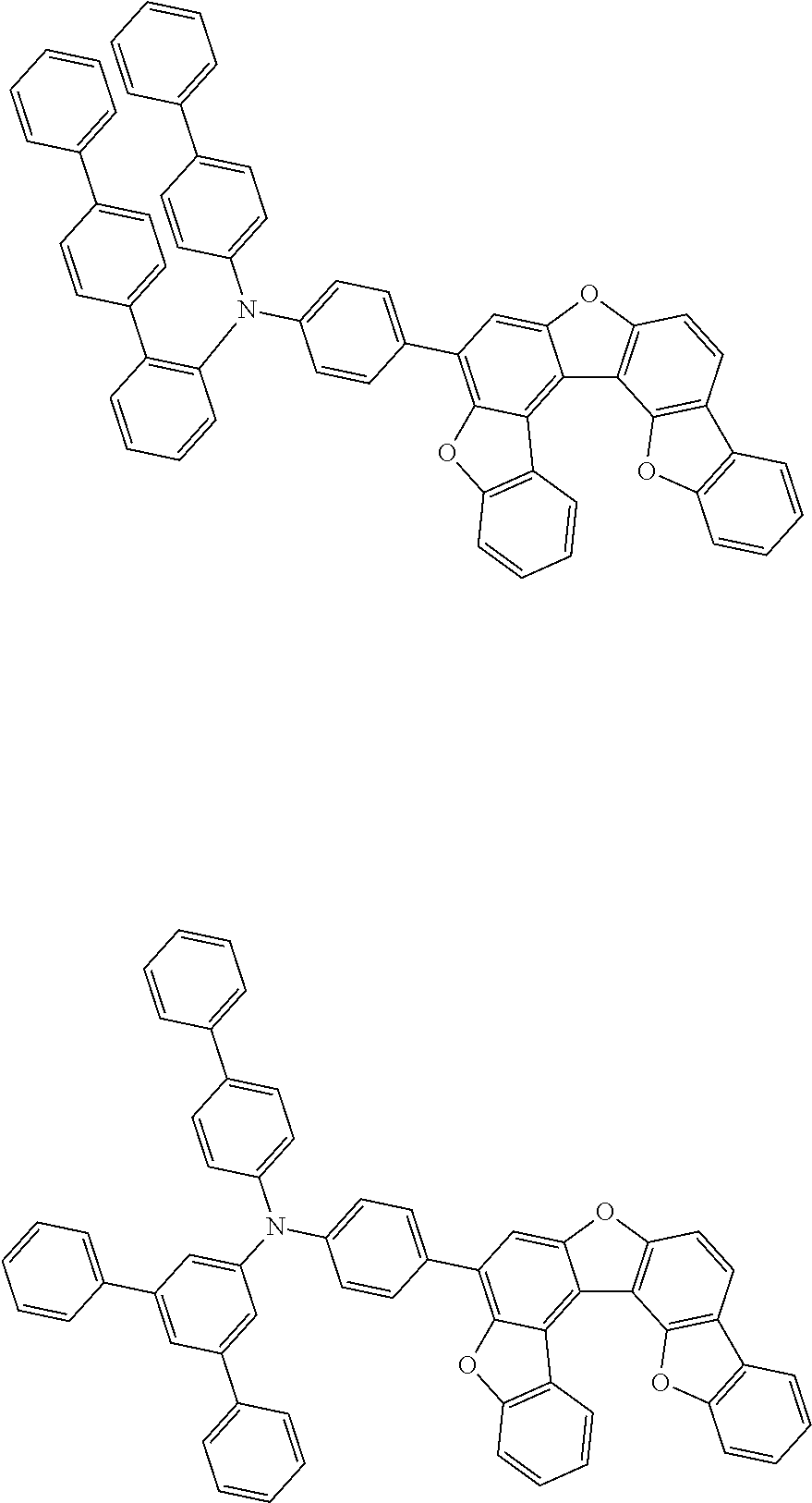


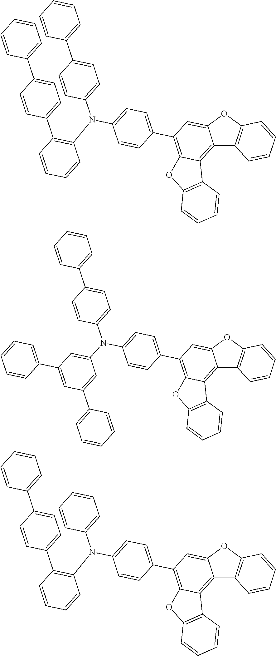


-
- in
Reaction Scheme 1, - the remaining definition except X′ are as defined above, and X′ is halogen, more preferably brorno, or chloro.
- in


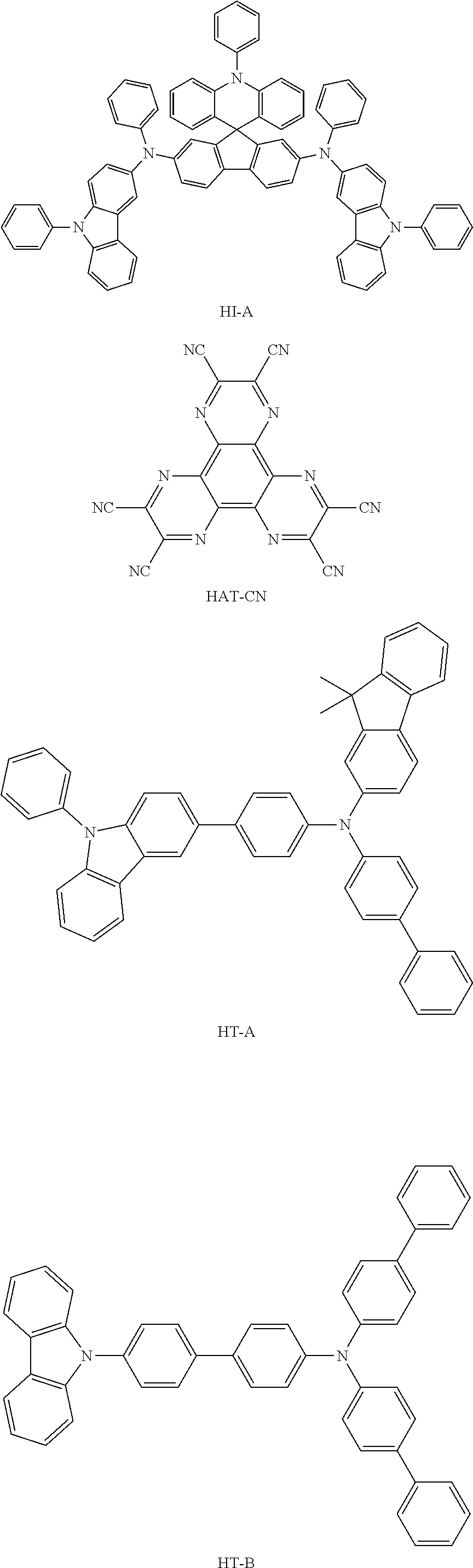


| TABLE 1 | |||||
| Voltage (V) | Efficiency (cd/A) | Lifetime (T95, hr) | |||
| Hole blocking layer | (@10 mA/cm2) | (@10 mA/cm2) | (@10 mA/cm2) | ||
| Test Example 1-1 | Compound 1-1 | 3.32 | 6.08 | 65 |
| Test Example 1-2 | Compound 1-2 | 3.33 | 6.07 | 60 |
| Test Example 1-3 | Compound 1-3 | 3.36 | 6.01 | 66 |
| Test Example 1-4 | Compound 1-4 | 3.38 | 6.10 | 68 |
| Test Example 1-5 | Compound 1-5 | 3.41 | 6.07 | 67 |
| Test Example 1-6 | Compound 1-6 | 3.45 | 6.06 | 65 |
| Test Example 1-7 | Compound 1-7 | 3.43 | 6.13 | 63 |
| Test Example 1-8 | Compound 1-8 | 3.47 | 6.02 | 61 |
| Comparative Test | ET-A | 4.21 | 5.11 | 40 |
| Example 1-1 | ||||
| Comparative Test | ET-C | 3.82 | 5.17 | 30 |
| Example 1-2 | ||||
| Comparative Test | ET-D | 3.73 | 5.29 | 20 |
| Example 1-3 | ||||

| TABLE 2 | |||||
| Electron blocking | Voltage (V) | Efficiency (cd/A) | Lifetime (T95, hr) | ||
| layer | (@10 mA/cm2) | (@10 mA/cm2) | (@10 mA/cm2) | ||
| Test Example 2-1 | Compound 2-1 | 3.41 | 6.07 | 65 |
| Test Example 2-2 | Compound 2-2 | 3.38 | 6.03 | 60 |
| Test Example 2-3 | Compound 2-3 | 3.39 | 6.08 | 66 |
| Test Example 2-4 | Compound 2-4 | 3.30 | 6.11 | 68 |
| Test Example 2-5 | Compound 2-5 | 3.46 | 6.07 | 67 |
| Test Example 2-6 | Compound 2-6 | 3.33 | 6.09 | 65 |
| Comparative Test | HT-B | 4.21 | 5.11 | 40 |
| Example 1-1 | ||||
| Comparative Test | HT-C | 6.13 | 3.82 | 15 |
| Example 2-1 | ||||
| Comparative Test | HT-D | 5.24 | 4.68 | 20 |
| Example 2-2 | ||||
| Comparative Test | HT-E | 4.82 | 5.21 | 42 |
| Example 2-3 | ||||
| Comparative Test | HT-F | 4.67 | 5.30 | 31 |
| Example 2-4 | ||||

| TABLE 3 | |||||
| Efficiency | |||||
| Voltage (V) | (cd/A) | Lifetime (T95, hr) | |||
| Dopant | (@10 mA/cm2) | (@10 mA/cm2) | (@10 mA/cm2) | ||
| Test Example 3-1 | Compound 3-1 | 3.45 | 6.12 | 70 |
| Test Example 3-2 | Compound 3-2 | 3.38 | 6.10 | 65 |
| Test Example 3-3 | Compound 3-3 | 3.42 | 6.21 | 68 |
| Test Example 3-4 | Compound 3-4 | 3.31 | 6.15 | 69 |
| Test Example 3-5 | Compound 3-5 | 3.40 | 6.18 | 67 |
| Comparative Test | BD | 4.21 | 5.11 | 40 |
| Example 1-1 | ||||
| Comparative Test | BD-A | 4.12 | 4.15 | 23 |
| Example 3-1 | ||||
| Comparative Test | BD-B | 6.81 | 2.21 | 12 |
| Example 3-2 | ||||
| Comparative Test | BD-C | 6.28 | 2.15 | 8 |
| Example 3-3 | ||||
| Comparative Test | BD-D | 6.31 | 2.38 | 10 |
| Example 3-4 | ||||


| TABLE 4 | |||||
| Voltage (V) | Efficiency(cd/A) | Lifetime (T95, hr) | |||
| Second host | (@10 mA/cm2) | (@10 mA/cm2) | (@20 mA/cm2) | ||
| Test Example 4-1 | Compound 1-1 | 3.85 | 57.51 | 130 |
| Test Example 4-2 | Compound 1-2 | 3.90 | 54.16 | 120 |
| Test Example 4-3 | Compound 1-4 | 3.91 | 56.33 | 110 |
| Test Example 4-4 | Compound 1-5 | 3.87 | 55.18 | 130 |
| Test Example 4-5 | Compound 1-8 | 3.81 | 57.39 | 140 |
| Comparative Test | GH-2-A | 4.56 | 32.11 | 80 |
| Example 4-1 | ||||
| Comparative Test | GH-2-B | 5.67 | 28.19 | 70 |
| Example 4-2 | ||||
| Comparative Test | GH-2-C | 6.65 | 36.55 | 60 |
| Example 4-3 | ||||
| [Explanation of Sign] |
| 1: substrate | 2: anode, | ||
| 3: light emitting layer | 4: cathode | ||
| 5: hole injection layer | 6: hole transport layer | ||
| 7: light emitting layer | 8: electron transport layer | ||
Claims (10)


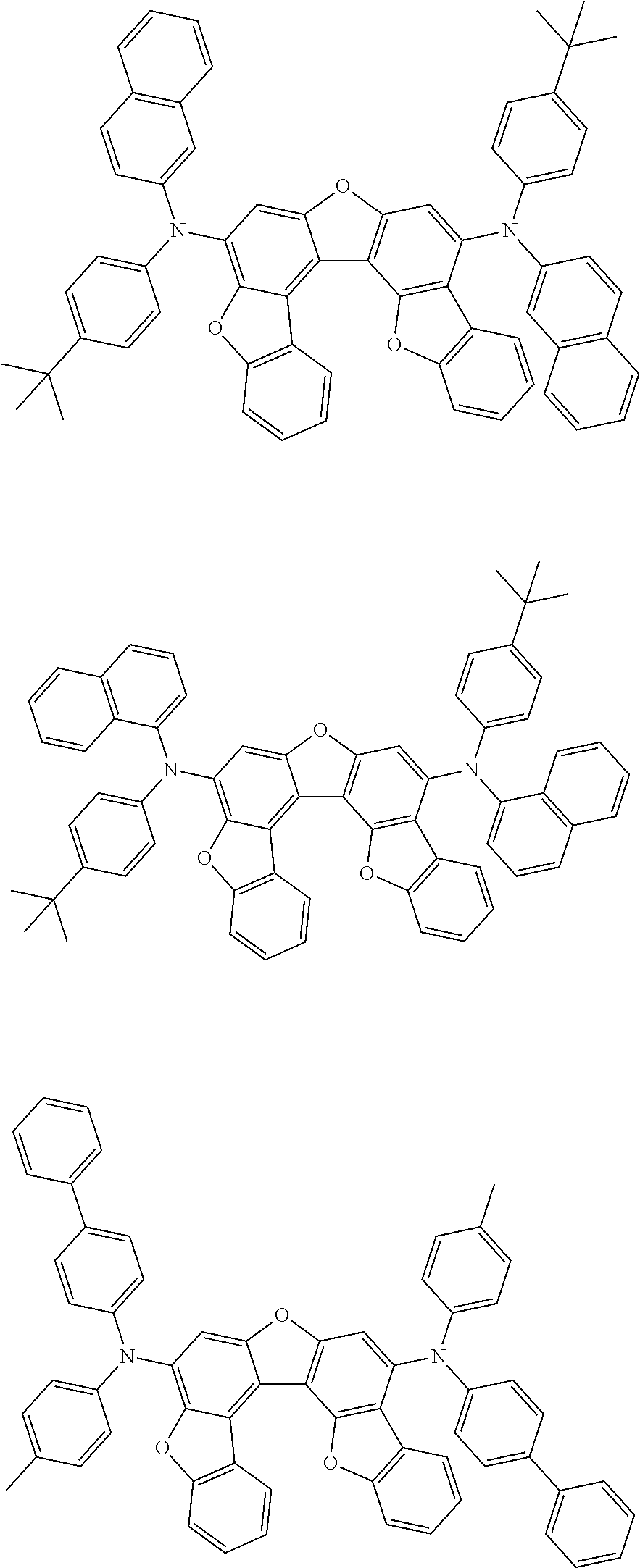


Applications Claiming Priority (3)
| Application Number | Priority Date | Filing Date | Title |
|---|---|---|---|
| KR10-2016-0170675 | 2016-12-14 | ||
| KR20160170675 | 2016-12-14 | ||
| PCT/KR2017/014686 WO2018110989A1 (en) | 2016-12-14 | 2017-12-14 | Heterocyclic compound and organic light emitting device comprising same |
Publications (2)
| Publication Number | Publication Date |
|---|---|
| US20190152985A1 US20190152985A1 (en) | 2019-05-23 |
| US10995098B2 true US10995098B2 (en) | 2021-05-04 |
Family
ID=62559642
Family Applications (1)
| Application Number | Title | Priority Date | Filing Date |
|---|---|---|---|
| US16/313,810 Active 2038-05-23 US10995098B2 (en) | 2016-12-14 | 2017-12-14 | Heterocyclic compound and organic light emitting device comprising the same |
Country Status (4)
| Country | Link |
|---|---|
| US (1) | US10995098B2 (en) |
| KR (1) | KR102044425B1 (en) |
| CN (1) | CN109641916B (en) |
| WO (1) | WO2018110989A1 (en) |
Families Citing this family (10)
| Publication number | Priority date | Publication date | Assignee | Title |
|---|---|---|---|---|
| KR102171076B1 (en) * | 2018-03-21 | 2020-10-28 | 삼성에스디아이 주식회사 | Composition for organic optoelectric device and organic optoelectric device and display device |
| CN110317206B (en) * | 2018-03-29 | 2021-10-22 | 江苏三月科技股份有限公司 | Compound with triarylamine as core and application thereof |
| KR102608414B1 (en) * | 2018-06-22 | 2023-12-01 | 삼성디스플레이 주식회사 | Condensed compound and organic light emitting device comprising the same |
| CN110407834A (en) * | 2019-07-26 | 2019-11-05 | 北京燕化集联光电技术有限公司 | A kind of OLED material of main part and the preparation method and application thereof |
| CN110734446A (en) * | 2019-10-30 | 2020-01-31 | 烟台显华化工科技有限公司 | organic compound and application thereof |
| KR20210092367A (en) * | 2020-01-15 | 2021-07-26 | 삼성디스플레이 주식회사 | Organic electroluminescence device and amine compound for organic electroluminescence device |
| KR20230013032A (en) * | 2020-05-20 | 2023-01-26 | 가부시키가이샤 한도오따이 에네루기 켄큐쇼 | Organic compounds, light emitting devices, light emitting devices, electronic devices, display devices, lighting devices |
| KR102554747B1 (en) * | 2020-11-17 | 2023-07-12 | 엘티소재주식회사 | Heterocyclic compound, organic light emitting device comprising the same, and composition for organic layer of organic light emitting device |
| KR20230092094A (en) * | 2021-12-16 | 2023-06-26 | 삼성에스디아이 주식회사 | Compound for organic optoelectronic device, composition for organic optoelectronic device, organic optoelectronic device and display device |
| WO2024063592A1 (en) * | 2022-09-23 | 2024-03-28 | 주식회사 엘지화학 | Novel compound and organic light-emitting device comprising same |
Citations (20)
| Publication number | Priority date | Publication date | Assignee | Title |
|---|---|---|---|---|
| KR20000051826A (en) | 1999-01-27 | 2000-08-16 | 성재갑 | New organomattalic complex molecule for the fabrication of organic light emitting diodes |
| KR20110018340A (en) | 2008-06-05 | 2011-02-23 | 이데미쓰 고산 가부시키가이샤 | Halogen compound, polycyclic compound, and organic electroluminescence element comprising the polycyclic compound |
| JP2012028548A (en) | 2010-07-23 | 2012-02-09 | Konica Minolta Holdings Inc | Material for organic electroluminescence element, and organic electroluminescence element, and display device and illuminating device using organic electroluminescence element |
| KR20130050237A (en) | 2011-11-07 | 2013-05-15 | 덕산하이메탈(주) | Compound for organic electronic element, organic electronic element using the same, and a electronic device thereof |
| KR20140128890A (en) | 2013-04-29 | 2014-11-06 | 주식회사 엘지화학 | Aromatic compounds and organic electronic device using the same |
| US20150034914A1 (en) | 2013-08-05 | 2015-02-05 | Han-Ill Lee | Organic compound and organic optoelectric device and display device |
| WO2015108325A1 (en) | 2014-01-16 | 2015-07-23 | 덕산네오룩스 주식회사 | Compound for organic electronic element, organic electronic element using same, and electronic device thereof |
| KR20150085766A (en) | 2014-01-16 | 2015-07-24 | 덕산네오룩스 주식회사 | Compound for organic electronic element, organic electronic element using the same, and an electronic device thereof |
| KR20160028737A (en) | 2014-09-04 | 2016-03-14 | 에스에프씨 주식회사 | An organoelectro luminescent compounds and organoelectro luminescent device using the same |
| US20160351816A1 (en) | 2015-05-27 | 2016-12-01 | Samsung Display Co., Ltd. | Organic light-emitting device |
| KR20170056425A (en) | 2015-11-13 | 2017-05-23 | 에스에프씨 주식회사 | Heterocyclic compound comprising aromatic amine group and organic light-emitting diode including the same |
| KR20170082459A (en) * | 2016-01-06 | 2017-07-14 | (주)피엔에이치테크 | An electroluminescent compound and an electroluminescent device comprising the same |
| KR20170086211A (en) | 2016-01-18 | 2017-07-26 | 에스에프씨 주식회사 | Organic light-emitting compounds and Organic light-emitting device comprising the same |
| KR20170086243A (en) | 2016-01-18 | 2017-07-26 | 에스에프씨 주식회사 | Organic light-emitting compounds and Organic light-emitting device comprising the same |
| US20170222160A1 (en) | 2016-02-03 | 2017-08-03 | Sfc Co., Ltd. | Organic light emitting compounds and organic light emitting devices including the same |
| US20180375035A1 (en) | 2017-06-23 | 2018-12-27 | Universal Display Corporation | Organic electroluminescent materials and devices |
| CN110088110A (en) | 2017-06-14 | 2019-08-02 | 株式会社Lg化学 | New compound and organic illuminating element comprising it |
| CN110248945A (en) | 2017-06-16 | 2019-09-17 | 株式会社Lg化学 | Anthracene derivant and organic luminescent device comprising it |
| CN110325537A (en) | 2017-06-16 | 2019-10-11 | 株式会社Lg化学 | Anthracene derivant and organic luminescent device comprising it |
| CN110892539A (en) | 2017-07-27 | 2020-03-17 | Sfc株式会社 | Organic light-emitting element capable of being driven at low voltage and having high efficiency and long life |
-
2017
- 2017-12-14 WO PCT/KR2017/014686 patent/WO2018110989A1/en active Application Filing
- 2017-12-14 KR KR1020170172267A patent/KR102044425B1/en active IP Right Grant
- 2017-12-14 US US16/313,810 patent/US10995098B2/en active Active
- 2017-12-14 CN CN201780050896.6A patent/CN109641916B/en active Active
Patent Citations (28)
| Publication number | Priority date | Publication date | Assignee | Title |
|---|---|---|---|---|
| KR20000051826A (en) | 1999-01-27 | 2000-08-16 | 성재갑 | New organomattalic complex molecule for the fabrication of organic light emitting diodes |
| KR20110018340A (en) | 2008-06-05 | 2011-02-23 | 이데미쓰 고산 가부시키가이샤 | Halogen compound, polycyclic compound, and organic electroluminescence element comprising the polycyclic compound |
| EP2301926A1 (en) | 2008-06-05 | 2011-03-30 | Idemitsu Kosan Co., Ltd. | Halogen compound, polycyclic compound, and organic electroluminescence element comprising the polycyclic compound |
| JP2012028548A (en) | 2010-07-23 | 2012-02-09 | Konica Minolta Holdings Inc | Material for organic electroluminescence element, and organic electroluminescence element, and display device and illuminating device using organic electroluminescence element |
| KR20130050237A (en) | 2011-11-07 | 2013-05-15 | 덕산하이메탈(주) | Compound for organic electronic element, organic electronic element using the same, and a electronic device thereof |
| KR20140128890A (en) | 2013-04-29 | 2014-11-06 | 주식회사 엘지화학 | Aromatic compounds and organic electronic device using the same |
| US20150034914A1 (en) | 2013-08-05 | 2015-02-05 | Han-Ill Lee | Organic compound and organic optoelectric device and display device |
| KR20150016845A (en) | 2013-08-05 | 2015-02-13 | 제일모직주식회사 | Organic compound and organic optoelectric device and display device |
| WO2015108325A1 (en) | 2014-01-16 | 2015-07-23 | 덕산네오룩스 주식회사 | Compound for organic electronic element, organic electronic element using same, and electronic device thereof |
| KR20150085766A (en) | 2014-01-16 | 2015-07-24 | 덕산네오룩스 주식회사 | Compound for organic electronic element, organic electronic element using the same, and an electronic device thereof |
| US20160380206A1 (en) | 2014-01-16 | 2016-12-29 | Duk San Neolux Co., Ltd. | Compound for organic electronic element, organic electronic element using the same, and an electronic device thereof |
| KR20160028737A (en) | 2014-09-04 | 2016-03-14 | 에스에프씨 주식회사 | An organoelectro luminescent compounds and organoelectro luminescent device using the same |
| US20160351816A1 (en) | 2015-05-27 | 2016-12-01 | Samsung Display Co., Ltd. | Organic light-emitting device |
| CN106206999A (en) | 2015-05-27 | 2016-12-07 | 三星显示有限公司 | Organic luminescent device |
| KR20170056425A (en) | 2015-11-13 | 2017-05-23 | 에스에프씨 주식회사 | Heterocyclic compound comprising aromatic amine group and organic light-emitting diode including the same |
| KR20170082459A (en) * | 2016-01-06 | 2017-07-14 | (주)피엔에이치테크 | An electroluminescent compound and an electroluminescent device comprising the same |
| KR20170086211A (en) | 2016-01-18 | 2017-07-26 | 에스에프씨 주식회사 | Organic light-emitting compounds and Organic light-emitting device comprising the same |
| KR20170086243A (en) | 2016-01-18 | 2017-07-26 | 에스에프씨 주식회사 | Organic light-emitting compounds and Organic light-emitting device comprising the same |
| US20170222160A1 (en) | 2016-02-03 | 2017-08-03 | Sfc Co., Ltd. | Organic light emitting compounds and organic light emitting devices including the same |
| CN107033128A (en) | 2016-02-03 | 2017-08-11 | Sfc有限责任公司 | Organic luminescent compounds and the organic light emitting apparatus including it |
| CN110088110A (en) | 2017-06-14 | 2019-08-02 | 株式会社Lg化学 | New compound and organic illuminating element comprising it |
| CN110325537A (en) | 2017-06-16 | 2019-10-11 | 株式会社Lg化学 | Anthracene derivant and organic luminescent device comprising it |
| CN110248945A (en) | 2017-06-16 | 2019-09-17 | 株式会社Lg化学 | Anthracene derivant and organic luminescent device comprising it |
| US20200028097A1 (en) | 2017-06-16 | 2020-01-23 | Lg Chem, Ltd. | Anthracene derivative and organic light-emitting device comprising same |
| CN109111488A (en) | 2017-06-23 | 2019-01-01 | 环球展览公司 | Electroluminescent organic material and device |
| US20180375035A1 (en) | 2017-06-23 | 2018-12-27 | Universal Display Corporation | Organic electroluminescent materials and devices |
| CN110892539A (en) | 2017-07-27 | 2020-03-17 | Sfc株式会社 | Organic light-emitting element capable of being driven at low voltage and having high efficiency and long life |
| US20200227644A1 (en) | 2017-07-27 | 2020-07-16 | Sfc Co., Ltd. | Organic light-emitting diode operable at low voltage with high efficiency and long lifetime |
Non-Patent Citations (1)
| Title |
|---|
| Berg et al., Quinone oligonnerization. An x-ray study; Tetrahedron Letters (1977), (21), 1831-4 (Year: 1977). * |
Also Published As
| Publication number | Publication date |
|---|---|
| WO2018110989A9 (en) | 2019-02-14 |
| WO2018110989A1 (en) | 2018-06-21 |
| CN109641916A (en) | 2019-04-16 |
| KR102044425B1 (en) | 2019-11-14 |
| KR20180068889A (en) | 2018-06-22 |
| US20190152985A1 (en) | 2019-05-23 |
| CN109641916B (en) | 2021-07-30 |
Similar Documents
| Publication | Publication Date | Title |
|---|---|---|
| US10995098B2 (en) | Heterocyclic compound and organic light emitting device comprising the same | |
| US10916710B2 (en) | Heterocyclic compound and organic light-emitting element comprising same | |
| US11251377B2 (en) | Organic light emitting device | |
| US20210184121A1 (en) | Heterocyclic compound and organic light-emitting device comprising same | |
| US9882145B2 (en) | Hetero ring compound and organic light emitting diode comprising same | |
| US10680182B2 (en) | Fluoranthene compound, and organic electronic device comprising same | |
| US9502669B2 (en) | Organic light emitting diode | |
| US10781366B2 (en) | Spiro compound and organic light-emitting device comprising same | |
| US11075342B2 (en) | Spiro-type compound and organic light emitting diode comprising same | |
| US20210217963A1 (en) | Organic light-emitting device | |
| US11456422B2 (en) | Compound and organic electroluminescent device comprising same | |
| US11189800B2 (en) | Heterocyclic compound and organic light emitting device comprising the same | |
| US10903431B2 (en) | Compound and organic electronic device comprising same | |
| US8597801B2 (en) | Heterocyclic compound, organic light-emitting device including the heterocyclic compound, and flat display device including the organic light-emitting device | |
| US10738034B2 (en) | Spiro compound and organic light-emitting device comprising same | |
| US20200144510A1 (en) | Organic optoelectronic device and display device | |
| US20220251118A1 (en) | Heterocyclic compound and organic light-emitting device comprising same | |
| US20200144508A1 (en) | Organic optoelectronic device and display device | |
| US10991887B2 (en) | Amine compound and organic light-emitting device comprising same | |
| US20210083198A1 (en) | Compound and organic light emitting device comprising same | |
| US10035765B2 (en) | Nitrogen-containing polycyclic compound and organic light emitting device using same | |
| US11968897B2 (en) | Heterocyclic compound and organic light emitting diode containing same | |
| US11261176B2 (en) | Amine-based compound and organic light emitting device using the same | |
| US20220029101A1 (en) | Organic light emitting diode | |
| US20210351360A1 (en) | Heterocyclic compound and organic light emitting device comprising same |
Legal Events
| Date | Code | Title | Description |
|---|---|---|---|
| AS | Assignment |
Owner name: LG CHEM, LTD., KOREA, REPUBLIC OF Free format text: ASSIGNMENT OF ASSIGNORS INTEREST;ASSIGNORS:SUH, SANG DUK;HONG, SUNG KIL;JEONG, KYUNG SEOK;REEL/FRAME:047863/0018 Effective date: 20181219 |
|
| FEPP | Fee payment procedure |
Free format text: ENTITY STATUS SET TO UNDISCOUNTED (ORIGINAL EVENT CODE: BIG.); ENTITY STATUS OF PATENT OWNER: LARGE ENTITY |
|
| STPP | Information on status: patent application and granting procedure in general |
Free format text: DOCKETED NEW CASE - READY FOR EXAMINATION |
|
| STPP | Information on status: patent application and granting procedure in general |
Free format text: PUBLICATIONS -- ISSUE FEE PAYMENT VERIFIED |
|
| STCF | Information on status: patent grant |
Free format text: PATENTED CASE |