US10991311B2 - Pixel circuit and method for driving the same, display panel and display apparatus - Google Patents
Pixel circuit and method for driving the same, display panel and display apparatus Download PDFInfo
- Publication number
- US10991311B2 US10991311B2 US16/807,378 US202016807378A US10991311B2 US 10991311 B2 US10991311 B2 US 10991311B2 US 202016807378 A US202016807378 A US 202016807378A US 10991311 B2 US10991311 B2 US 10991311B2
- Authority
- US
- United States
- Prior art keywords
- transistor
- control signal
- voltage
- pixel circuit
- period
- Prior art date
- Legal status (The legal status is an assumption and is not a legal conclusion. Google has not performed a legal analysis and makes no representation as to the accuracy of the status listed.)
- Active
Links
Images


Classifications
-
- G—PHYSICS
- G09—EDUCATION; CRYPTOGRAPHY; DISPLAY; ADVERTISING; SEALS
- G09G—ARRANGEMENTS OR CIRCUITS FOR CONTROL OF INDICATING DEVICES USING STATIC MEANS TO PRESENT VARIABLE INFORMATION
- G09G3/00—Control arrangements or circuits, of interest only in connection with visual indicators other than cathode-ray tubes
- G09G3/20—Control arrangements or circuits, of interest only in connection with visual indicators other than cathode-ray tubes for presentation of an assembly of a number of characters, e.g. a page, by composing the assembly by combination of individual elements arranged in a matrix no fixed position being assigned to or needed to be assigned to the individual characters or partial characters
- G09G3/22—Control arrangements or circuits, of interest only in connection with visual indicators other than cathode-ray tubes for presentation of an assembly of a number of characters, e.g. a page, by composing the assembly by combination of individual elements arranged in a matrix no fixed position being assigned to or needed to be assigned to the individual characters or partial characters using controlled light sources
- G09G3/30—Control arrangements or circuits, of interest only in connection with visual indicators other than cathode-ray tubes for presentation of an assembly of a number of characters, e.g. a page, by composing the assembly by combination of individual elements arranged in a matrix no fixed position being assigned to or needed to be assigned to the individual characters or partial characters using controlled light sources using electroluminescent panels
- G09G3/32—Control arrangements or circuits, of interest only in connection with visual indicators other than cathode-ray tubes for presentation of an assembly of a number of characters, e.g. a page, by composing the assembly by combination of individual elements arranged in a matrix no fixed position being assigned to or needed to be assigned to the individual characters or partial characters using controlled light sources using electroluminescent panels semiconductive, e.g. using light-emitting diodes [LED]
- G09G3/3208—Control arrangements or circuits, of interest only in connection with visual indicators other than cathode-ray tubes for presentation of an assembly of a number of characters, e.g. a page, by composing the assembly by combination of individual elements arranged in a matrix no fixed position being assigned to or needed to be assigned to the individual characters or partial characters using controlled light sources using electroluminescent panels semiconductive, e.g. using light-emitting diodes [LED] organic, e.g. using organic light-emitting diodes [OLED]
- G09G3/3225—Control arrangements or circuits, of interest only in connection with visual indicators other than cathode-ray tubes for presentation of an assembly of a number of characters, e.g. a page, by composing the assembly by combination of individual elements arranged in a matrix no fixed position being assigned to or needed to be assigned to the individual characters or partial characters using controlled light sources using electroluminescent panels semiconductive, e.g. using light-emitting diodes [LED] organic, e.g. using organic light-emitting diodes [OLED] using an active matrix
- G09G3/3258—Control arrangements or circuits, of interest only in connection with visual indicators other than cathode-ray tubes for presentation of an assembly of a number of characters, e.g. a page, by composing the assembly by combination of individual elements arranged in a matrix no fixed position being assigned to or needed to be assigned to the individual characters or partial characters using controlled light sources using electroluminescent panels semiconductive, e.g. using light-emitting diodes [LED] organic, e.g. using organic light-emitting diodes [OLED] using an active matrix with pixel circuitry controlling the voltage across the light-emitting element
-
- G—PHYSICS
- G09—EDUCATION; CRYPTOGRAPHY; DISPLAY; ADVERTISING; SEALS
- G09G—ARRANGEMENTS OR CIRCUITS FOR CONTROL OF INDICATING DEVICES USING STATIC MEANS TO PRESENT VARIABLE INFORMATION
- G09G3/00—Control arrangements or circuits, of interest only in connection with visual indicators other than cathode-ray tubes
- G09G3/20—Control arrangements or circuits, of interest only in connection with visual indicators other than cathode-ray tubes for presentation of an assembly of a number of characters, e.g. a page, by composing the assembly by combination of individual elements arranged in a matrix no fixed position being assigned to or needed to be assigned to the individual characters or partial characters
- G09G3/22—Control arrangements or circuits, of interest only in connection with visual indicators other than cathode-ray tubes for presentation of an assembly of a number of characters, e.g. a page, by composing the assembly by combination of individual elements arranged in a matrix no fixed position being assigned to or needed to be assigned to the individual characters or partial characters using controlled light sources
- G09G3/30—Control arrangements or circuits, of interest only in connection with visual indicators other than cathode-ray tubes for presentation of an assembly of a number of characters, e.g. a page, by composing the assembly by combination of individual elements arranged in a matrix no fixed position being assigned to or needed to be assigned to the individual characters or partial characters using controlled light sources using electroluminescent panels
- G09G3/32—Control arrangements or circuits, of interest only in connection with visual indicators other than cathode-ray tubes for presentation of an assembly of a number of characters, e.g. a page, by composing the assembly by combination of individual elements arranged in a matrix no fixed position being assigned to or needed to be assigned to the individual characters or partial characters using controlled light sources using electroluminescent panels semiconductive, e.g. using light-emitting diodes [LED]
- G09G3/3208—Control arrangements or circuits, of interest only in connection with visual indicators other than cathode-ray tubes for presentation of an assembly of a number of characters, e.g. a page, by composing the assembly by combination of individual elements arranged in a matrix no fixed position being assigned to or needed to be assigned to the individual characters or partial characters using controlled light sources using electroluminescent panels semiconductive, e.g. using light-emitting diodes [LED] organic, e.g. using organic light-emitting diodes [OLED]
- G09G3/3225—Control arrangements or circuits, of interest only in connection with visual indicators other than cathode-ray tubes for presentation of an assembly of a number of characters, e.g. a page, by composing the assembly by combination of individual elements arranged in a matrix no fixed position being assigned to or needed to be assigned to the individual characters or partial characters using controlled light sources using electroluminescent panels semiconductive, e.g. using light-emitting diodes [LED] organic, e.g. using organic light-emitting diodes [OLED] using an active matrix
- G09G3/3233—Control arrangements or circuits, of interest only in connection with visual indicators other than cathode-ray tubes for presentation of an assembly of a number of characters, e.g. a page, by composing the assembly by combination of individual elements arranged in a matrix no fixed position being assigned to or needed to be assigned to the individual characters or partial characters using controlled light sources using electroluminescent panels semiconductive, e.g. using light-emitting diodes [LED] organic, e.g. using organic light-emitting diodes [OLED] using an active matrix with pixel circuitry controlling the current through the light-emitting element
-
- G—PHYSICS
- G09—EDUCATION; CRYPTOGRAPHY; DISPLAY; ADVERTISING; SEALS
- G09G—ARRANGEMENTS OR CIRCUITS FOR CONTROL OF INDICATING DEVICES USING STATIC MEANS TO PRESENT VARIABLE INFORMATION
- G09G3/00—Control arrangements or circuits, of interest only in connection with visual indicators other than cathode-ray tubes
- G09G3/20—Control arrangements or circuits, of interest only in connection with visual indicators other than cathode-ray tubes for presentation of an assembly of a number of characters, e.g. a page, by composing the assembly by combination of individual elements arranged in a matrix no fixed position being assigned to or needed to be assigned to the individual characters or partial characters
- G09G3/22—Control arrangements or circuits, of interest only in connection with visual indicators other than cathode-ray tubes for presentation of an assembly of a number of characters, e.g. a page, by composing the assembly by combination of individual elements arranged in a matrix no fixed position being assigned to or needed to be assigned to the individual characters or partial characters using controlled light sources
- G09G3/30—Control arrangements or circuits, of interest only in connection with visual indicators other than cathode-ray tubes for presentation of an assembly of a number of characters, e.g. a page, by composing the assembly by combination of individual elements arranged in a matrix no fixed position being assigned to or needed to be assigned to the individual characters or partial characters using controlled light sources using electroluminescent panels
- G09G3/32—Control arrangements or circuits, of interest only in connection with visual indicators other than cathode-ray tubes for presentation of an assembly of a number of characters, e.g. a page, by composing the assembly by combination of individual elements arranged in a matrix no fixed position being assigned to or needed to be assigned to the individual characters or partial characters using controlled light sources using electroluminescent panels semiconductive, e.g. using light-emitting diodes [LED]
- G09G3/3208—Control arrangements or circuits, of interest only in connection with visual indicators other than cathode-ray tubes for presentation of an assembly of a number of characters, e.g. a page, by composing the assembly by combination of individual elements arranged in a matrix no fixed position being assigned to or needed to be assigned to the individual characters or partial characters using controlled light sources using electroluminescent panels semiconductive, e.g. using light-emitting diodes [LED] organic, e.g. using organic light-emitting diodes [OLED]
- G09G3/3225—Control arrangements or circuits, of interest only in connection with visual indicators other than cathode-ray tubes for presentation of an assembly of a number of characters, e.g. a page, by composing the assembly by combination of individual elements arranged in a matrix no fixed position being assigned to or needed to be assigned to the individual characters or partial characters using controlled light sources using electroluminescent panels semiconductive, e.g. using light-emitting diodes [LED] organic, e.g. using organic light-emitting diodes [OLED] using an active matrix
-
- G—PHYSICS
- G09—EDUCATION; CRYPTOGRAPHY; DISPLAY; ADVERTISING; SEALS
- G09G—ARRANGEMENTS OR CIRCUITS FOR CONTROL OF INDICATING DEVICES USING STATIC MEANS TO PRESENT VARIABLE INFORMATION
- G09G2300/00—Aspects of the constitution of display devices
- G09G2300/04—Structural and physical details of display devices
- G09G2300/0421—Structural details of the set of electrodes
- G09G2300/0426—Layout of electrodes and connections
-
- G—PHYSICS
- G09—EDUCATION; CRYPTOGRAPHY; DISPLAY; ADVERTISING; SEALS
- G09G—ARRANGEMENTS OR CIRCUITS FOR CONTROL OF INDICATING DEVICES USING STATIC MEANS TO PRESENT VARIABLE INFORMATION
- G09G2300/00—Aspects of the constitution of display devices
- G09G2300/04—Structural and physical details of display devices
- G09G2300/0421—Structural details of the set of electrodes
- G09G2300/043—Compensation electrodes or other additional electrodes in matrix displays related to distortions or compensation signals, e.g. for modifying TFT threshold voltage in column driver
-
- G—PHYSICS
- G09—EDUCATION; CRYPTOGRAPHY; DISPLAY; ADVERTISING; SEALS
- G09G—ARRANGEMENTS OR CIRCUITS FOR CONTROL OF INDICATING DEVICES USING STATIC MEANS TO PRESENT VARIABLE INFORMATION
- G09G2300/00—Aspects of the constitution of display devices
- G09G2300/08—Active matrix structure, i.e. with use of active elements, inclusive of non-linear two terminal elements, in the pixels together with light emitting or modulating elements
- G09G2300/0809—Several active elements per pixel in active matrix panels
- G09G2300/0819—Several active elements per pixel in active matrix panels used for counteracting undesired variations, e.g. feedback or autozeroing
-
- G—PHYSICS
- G09—EDUCATION; CRYPTOGRAPHY; DISPLAY; ADVERTISING; SEALS
- G09G—ARRANGEMENTS OR CIRCUITS FOR CONTROL OF INDICATING DEVICES USING STATIC MEANS TO PRESENT VARIABLE INFORMATION
- G09G2300/00—Aspects of the constitution of display devices
- G09G2300/08—Active matrix structure, i.e. with use of active elements, inclusive of non-linear two terminal elements, in the pixels together with light emitting or modulating elements
- G09G2300/0809—Several active elements per pixel in active matrix panels
- G09G2300/0842—Several active elements per pixel in active matrix panels forming a memory circuit, e.g. a dynamic memory with one capacitor
-
- G—PHYSICS
- G09—EDUCATION; CRYPTOGRAPHY; DISPLAY; ADVERTISING; SEALS
- G09G—ARRANGEMENTS OR CIRCUITS FOR CONTROL OF INDICATING DEVICES USING STATIC MEANS TO PRESENT VARIABLE INFORMATION
- G09G2320/00—Control of display operating conditions
- G09G2320/04—Maintaining the quality of display appearance
- G09G2320/043—Preventing or counteracting the effects of ageing
- G09G2320/045—Compensation of drifts in the characteristics of light emitting or modulating elements
Definitions
- OLED Organic Light Emitting Diode
- DTFT Driving Thin Film Transistor
- stability of a DTFT manufactured by using a Low Temperature Poly-silicon (LTPS) process generally may not be maintained, and a threshold voltage Vth and mobility of the DTFT may shift under action of Excimer Laser Annealing (ELA) crystallization, long-term pressure, temperature changes, etc.
- ELA Excimer Laser Annealing
- complex pixel circuits such as 7T1C (having seven transistors and one capacitor) are required to perform compensation for the DTFT to ensure that the DTFT outputs stable current under different operating conditions, thereby ensuring the display effect and lifetime of an OLED display.
- the above pixel circuits may not be used to perform driving to realize display with a high PPI.
- a pixel circuit comprising: a storage capacitor having a first terminal electrically coupled to a first control signal terminal for providing a first control signal; a first transistor having a first electrode electrically coupled to a first voltage signal terminal, and a gate electrically coupled to a second terminal of the storage capacitor; a second transistor having a first electrode electrically coupled to the gate of the first transistor, a second electrode electrically coupled to a second electrode of the first transistor, and a gate electrically coupled to a second control signal terminal for providing a second control signal; and a light emitting element having a first electrode electrically coupled to the second electrode of the second transistor, and a second electrode electrically coupled to a second voltage signal terminal for providing a second voltage signal.
- the second transistor comprises a double-gate thin film transistor, wherein two gates of the double-gate thin film transistor are both electrically coupled to the second control signal terminal.
- both of the first transistor and the second transistor are polycrystalline thin film transistors or zinc oxide thin film transistors.
- the first transistor is a P-type or N-type thin film transistor
- the second transistor is a P-type or N-type thin film transistor
- the first electrode of the first transistor is a drain
- the second electrode of the first transistor is a source
- a method for driving a pixel circuit comprising: turning on, during a first period, the first transistor by using a first control signal; applying, during a second period, a data voltage Vdata to the first voltage signal terminal, so that a voltage at the gate of the first transistor is Vdata+Vth, wherein Vth is a threshold voltage of the first transistor; and applying, during a third period, a first voltage ELVDD to the first voltage signal terminal, so that a voltage between the first electrode and the gate of the first transistor is Vdata+Vth ⁇ ELVDD, wherein ELVDD>Vdata.
- the method for driving a pixel circuit further comprises: when both of the first transistor and the second transistor are P-type thin film transistors, providing, during a first sub-period of the first period, the first control signal at a high level, applying a low-level voltage to the first voltage signal terminal, and providing the second control signal at a low level, to pull down a voltage at the gate of the first transistor; and providing, during a second sub-period of the first period, the first control signal at a high level, and providing the second control signal at a high level.
- the method for driving a pixel circuit further comprises: when both of the first transistor and the second transistor are P-type thin film transistors, providing, during a first sub-period of the second period, the second control signal at a low level, providing the first control signal at a low level, and applying a data voltage Vdata to the first voltage signal terminal, so that the voltage at the gate of the first transistor is Vdata+Vth; and providing, during a second sub-period of the second period, the second control signal at a high level, and providing the first control signal at a high level.
- the method for driving a pixel circuit further comprises: when both of the first transistor and the second transistor are P-type thin film transistors, during the third period, providing the first control signal at a low level, and applying a first voltage ELVDD to the first voltage signal terminal to drive the light emitting element to emit light.
- a display panel comprising: the pixel circuit according to the embodiments described above; a first driver configured to output the first control signal and the second control signal to the pixel circuit; and a second driver configured to apply corresponding voltage signals to the first voltage signal terminal and the second voltage signal terminal.
- a display apparatus comprising: a housing; and the display panel according to the embodiments described above, wherein the housing is disposed opposite to the display panel.
- FIG. 1 is a schematic structural diagram of a pixel circuit according to an exemplary embodiment of the present disclosure
- FIG. 2 is a schematic structural diagram of a pixel circuit according to another exemplary embodiment of the present disclosure.
- FIG. 3 is a schematic structural diagram of a pixel circuit according to yet another exemplary embodiment of the present disclosure.
- FIG. 4 is a schematic structural diagram of a pixel circuit according to still another exemplary embodiment of the present disclosure.
- FIG. 5 is a schematic structural diagram of a pixel circuit according to another example of the present disclosure.
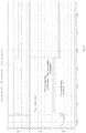
- FIG. 6B is a schematic diagram of a driving timing during an operation of a pixel circuit according to an embodiment of the present disclosure
- FIG. 7 is an analog waveform diagram of a pixel circuit according to an embodiment of the present disclosure when Vdata has a value of 0V to 3V;
- FIG. 8 is an analog waveform diagram of a pixel circuit according to an embodiment of the present disclosure when Vth has a value of ⁇ 1V to 1V;
- FIG. 10 is a structural block diagram of a display panel according to an embodiment of the present disclosure.
- FIG. 11 is a structural block diagram of a display apparatus according to an embodiment of the present disclosure.
- FIG. 1 is a schematic structural diagram of a pixel circuit according to an embodiment of the present disclosure.
- the pixel circuit 100 may comprise a storage capacitor C, a first transistor T 1 , a second transistor T 2 , and a light emitting element D.
- the organic light emitting diode D has a first electrode electrically coupled to the second node N 2 , and a second electrode electrically coupled to a second voltage signal terminal.
- the first electrode of the organic light emitting diode D may be an anode
- the second electrode of the organic light emitting diode D may be a cathode
- a low-level ELVSS may be applied to the second voltage signal terminal.
- the second transistor T 2 may be a double-gate thin film transistor. Both of two gates of the double-gate thin film transistor are electrically coupled to the second control signal terminal Gate for providing the second control signal.
- both of the first transistor T 1 and the second transistor T 2 may be polycrystalline thin film transistors, for example, Low Temperature Poly-silicon (LTPS) Thin Film Transistors (TFTs), Low Temperature Polycrystalline Oxide (LTPO) TFTs etc., or may also be zinc oxide thin film transistors, for example, Indium Gallium Zinc Oxide (IGZO) TFTs.
- LTPS Low Temperature Poly-silicon
- TFTs Thin Film Transistors
- LTPO Low Temperature Polycrystalline Oxide
- IGZO Indium Gallium Zinc Oxide
- the first transistor T 1 may be a polycrystalline thin film transistor
- the second transistor T 2 may be a zinc oxide thin film transistor
- the first transistor T 1 may be a zinc oxide thin film transistor
- the second transistor T 2 may be a polycrystalline thin film transistor
- both of the first transistor T 1 and the second transistor T 2 are P-type thin film transistors.
- both of the first transistor T 1 and the second transistor T 2 are N-type thin film transistors.
- the first transistor T 1 is a P-type thin film transistor
- the second transistor T 2 is an N-type thin film transistor.
- the first transistor T 1 is an N-type thin film transistor
- the second transistor T 2 is a P-type thin film transistor.
- the first phase P 1 may comprise a sub-period P 11 and a sub-period P 12 .
- a second control signal input at the second control signal terminal Gate is at a low level
- the second transistor T 2 is turned on
- a first control signal provided at the first control signal terminal EM is at a high level
- a voltage at the first node N 1 is pulled up through coupling of the storage capacitor C.
- both of the first voltage signal terminal and the second voltage signal terminal are at low-level voltages, to pull down voltages at the first node N 1 and the second node N 2 to complete initialization at the first node N 1 .
- the second phase P 2 may comprise a sub-period P 21 and a sub-period P 22 .
- the second control signal is at a low level, so that the second transistor T 2 is turned on.
- the first control signal is at a low level, and the potential at the first node N 1 is coupled to a low voltage through the storage capacitor C, so that the first transistor T 1 is turned on.
- the first voltage signal terminal provides a data voltage Vdata. Since both of the first transistor T 1 and the second transistor T 2 are turned on, the voltage at the first node N 1 is finally Vdata+Vth, so as to realize the extraction of Vth.
- the second control signal is at a high level, so that the second transistor T 2 is turned off, and the first node N 1 is floating.
- the first control signal is at a high level, and thus the voltage at the first node N 1 is (EM_H ⁇ EM_L)+Vdata+Vth. It may be understood that in a case that the first transistor T 1 is a P-type transistor, Vth has a negative value.
- EM_H is a high-level voltage value of the first control signal
- EM_L is a low-level voltage value of the first control signal.
- the first control signal is at a low level, so that the voltage V N1 at the first node N 1 is coupled to Vdata+Vth through the storage capacitor C.
- ⁇ field effect mobility of the first transistor T 1
- Cox is capacitance per unit area of the structure of the first transistor T 1
- W/L is a width-to-length ratio of a channel of the first transistor T 1 .
- the pixel circuit according to the embodiment of the present disclosure may not only realize the function of compensating for Vth of the pixel circuit, but also has a small footprint, and may be widely used in display of an OLED with a high PPI.
- the method for driving a pixel circuit may comprise the following steps.
- a first control signal is at a high level, a low-level voltage is applied to the first voltage signal terminal, and a second control signal is at a low level, to pull down a voltage at the gate of the first transistor; and during a second sub-period of the first period, the first control signal is at a high level and the second control signal is at a high level.
- the second control signal is at a low level, the first control signal is at a low level, and a data voltage Vdata is applied to the first voltage signal terminal, so that the voltage at the gate of the first transistor is Vdata+Vth; and during a second sub-period of the second period, the second control signal is at a high level, and the first control signal is at a high level.
- the first control signal is at a low level, and a first voltage ELVDD is applied to the first voltage signal terminal to drive the light emitting element to emit light.
- the method for driving a pixel circuit according to the embodiment of the present disclosure may not only realize the function of compensating for Vth, but also has a small footprint, and may be widely used in display of an OLED with a high PPI.
- FIG. 10 is a structural block diagram of a display panel according to an embodiment of the present disclosure.
- the display panel 1000 may comprise a pixel circuit 1100 according to the embodiment of the present disclosure, a first driver 1200 , and a second driver 1300 .
- the pixel circuit described above is used, which may not only realize the function of compensating for Vth, but also has a small footprint, and may be widely used in display of an OLED with a high PPI.
- the display panel comprising the pixel circuit described above is used, which may not only realize the function of compensating for Vth, but also has a small footprint, and may be widely used in display of an OLED with a high PPI.
- first and second are used for descriptive purposes only, and are not to be construed as indicating or implying relative importance or implicitly indicating a number of indicated technical features.
- features defined by “first” and “second” may explicitly or implicitly include at least one of the features.
- Coupled should be broadly understood, for example, it may be fixed coupling, detachable coupling, or integrated coupling; or it may be direct coupling, or indirect coupling through an intermediate medium; or it may be internal connection between two elements or interaction between two elements, unless explicitly defined otherwise.
- Specific meanings of the above terms in the present disclosure may be understood by those of ordinary skill in the art according to specific situations.
Landscapes
- Engineering & Computer Science (AREA)
- Physics & Mathematics (AREA)
- Computer Hardware Design (AREA)
- General Physics & Mathematics (AREA)
- Theoretical Computer Science (AREA)
- Electroluminescent Light Sources (AREA)
- Control Of Indicators Other Than Cathode Ray Tubes (AREA)
- Control Of El Displays (AREA)
Abstract
Description
Claims (9)
Applications Claiming Priority (2)
| Application Number | Priority Date | Filing Date | Title |
|---|---|---|---|
| CN201910646657.8 | 2019-07-17 | ||
| CN201910646657.8A CN110364117B (en) | 2019-07-17 | 2019-07-17 | Pixel circuit and driving method thereof, display panel and display device |
Publications (2)
| Publication Number | Publication Date |
|---|---|
| US20210056903A1 US20210056903A1 (en) | 2021-02-25 |
| US10991311B2 true US10991311B2 (en) | 2021-04-27 |
Family
ID=68220988
Family Applications (1)
| Application Number | Title | Priority Date | Filing Date |
|---|---|---|---|
| US16/807,378 Active US10991311B2 (en) | 2019-07-17 | 2020-03-03 | Pixel circuit and method for driving the same, display panel and display apparatus |
Country Status (2)
| Country | Link |
|---|---|
| US (1) | US10991311B2 (en) |
| CN (1) | CN110364117B (en) |
Cited By (1)
| Publication number | Priority date | Publication date | Assignee | Title |
|---|---|---|---|---|
| US11568811B2 (en) * | 2020-06-22 | 2023-01-31 | Lg Display Co., Ltd. | Electroluminescence display apparatus |
Families Citing this family (3)
| Publication number | Priority date | Publication date | Assignee | Title |
|---|---|---|---|---|
| CN112133253A (en) * | 2020-09-22 | 2020-12-25 | Oppo广东移动通信有限公司 | Pixel drive circuit, display device, and drive method |
| CN114333696A (en) * | 2021-12-28 | 2022-04-12 | Tcl华星光电技术有限公司 | Pixel circuit, control method thereof, array substrate and display panel |
| CN117456930A (en) * | 2023-10-20 | 2024-01-26 | 京东方科技集团股份有限公司 | Pixel circuit, display device and driving method |
Citations (23)
| Publication number | Priority date | Publication date | Assignee | Title |
|---|---|---|---|---|
| US20040257359A1 (en) * | 2003-06-19 | 2004-12-23 | Sharp Kabushiki Kaisha | Display Element and display device |
| US20080303749A1 (en) | 2005-12-13 | 2008-12-11 | Koninklijke Philips Electronics, N.V. | Active Matrix Array Device |
| US20110050736A1 (en) * | 2009-09-01 | 2011-03-03 | National Taiwan University Of Science And Technology | Pixel and illuminating device thereof |
| US20110234957A1 (en) * | 2009-09-28 | 2011-09-29 | Casio Computer Co., Ltd. | Display apparatus |
| US20110279437A1 (en) * | 2010-05-11 | 2011-11-17 | Naoaki Komiya | Organic light emitting display and driving method thereof |
| US20120293479A1 (en) * | 2011-05-19 | 2012-11-22 | Han Sang-Myeon | Pixel, Display Device Including The Pixel, And Driving Method Of The Display Device |
| CN103295519A (en) | 2012-03-05 | 2013-09-11 | 群康科技(深圳)有限公司 | Displayer and pixel driving method |
| CN104123912A (en) | 2014-07-03 | 2014-10-29 | 京东方科技集团股份有限公司 | Pixel circuit and driving method thereof, and display device |
| US20150002557A1 (en) * | 2013-07-01 | 2015-01-01 | Samsung Display Co., Ltd. | Pixel circuit, driving method, and display apparatus having the same |
| US20150062195A1 (en) * | 2013-08-30 | 2015-03-05 | Samsung Display Co., Ltd. | Electroluminescence display device and driving method thereof |
| US20150221252A1 (en) * | 2013-08-07 | 2015-08-06 | Boe Technology Group Co., Ltd. | Ac drive circuit for oled, drive method and display apparatus |
| US20160104418A1 (en) * | 2014-10-10 | 2016-04-14 | Samsung Display Co., Ltd. | Timing controller, organic light-emitting diode (oled) display having the same and method for driving the oled display |
| US20160140900A1 (en) * | 2014-05-04 | 2016-05-19 | Beijing Boe Optoelectronics Technology Co., Ltd. | Pixel driving circuit, driving method, array substrate and display apparatus |
| US20160274692A1 (en) * | 2014-05-29 | 2016-09-22 | Boe Technology Group Co., Ltd. | Pixel circuit, method for driving the same, organic light-emitting diode display panel, and display device |
| US20160351124A1 (en) * | 2015-05-28 | 2016-12-01 | Lg Display Co., Ltd. | Organic Light Emitting Display |
| CN106531067A (en) | 2016-12-23 | 2017-03-22 | 上海天马有机发光显示技术有限公司 | Pixel circuit and driving method thereof, and display device |
| US20170110049A1 (en) | 2015-10-19 | 2017-04-20 | Samsung Display Co., Ltd. | Organic light-emitting display apparatus |
| US20170162115A1 (en) * | 2015-12-03 | 2017-06-08 | Innolux Corporation | Driving circuit of active-matrix organic light-emitting diode with hybrid transistors |
| US20170330511A1 (en) * | 2015-08-21 | 2017-11-16 | Boe Technology Group Co., Ltd. | Pixel Circuit And Driving Method Thereof, Array Substrate, Display Panel And Display Device |
| US20180047337A1 (en) * | 2017-04-28 | 2018-02-15 | Shanghai Tianma AM-OLED Co., Ltd. | Display panel, display device, and method for driving a pixel circuit |
| CN108520719A (en) | 2018-04-20 | 2018-09-11 | 芯颖科技有限公司 | Drive control circuit and method |
| US20190130846A1 (en) | 2017-10-31 | 2019-05-02 | Lg Display Co., Ltd. | Electroluminescent Display |
| US20190266950A1 (en) * | 2018-02-28 | 2019-08-29 | Shenzhen China Star Optoelectronics Technology Co., Ltd. | Amoled pixel driving circuit and driving method |
-
2019
- 2019-07-17 CN CN201910646657.8A patent/CN110364117B/en active Active
-
2020
- 2020-03-03 US US16/807,378 patent/US10991311B2/en active Active
Patent Citations (30)
| Publication number | Priority date | Publication date | Assignee | Title |
|---|---|---|---|---|
| US20040257359A1 (en) * | 2003-06-19 | 2004-12-23 | Sharp Kabushiki Kaisha | Display Element and display device |
| US20080303749A1 (en) | 2005-12-13 | 2008-12-11 | Koninklijke Philips Electronics, N.V. | Active Matrix Array Device |
| CN101331533A (en) | 2005-12-13 | 2008-12-24 | 皇家飞利浦电子股份有限公司 | Active Matrix Array Device |
| US20110050736A1 (en) * | 2009-09-01 | 2011-03-03 | National Taiwan University Of Science And Technology | Pixel and illuminating device thereof |
| US20110234957A1 (en) * | 2009-09-28 | 2011-09-29 | Casio Computer Co., Ltd. | Display apparatus |
| US20110279437A1 (en) * | 2010-05-11 | 2011-11-17 | Naoaki Komiya | Organic light emitting display and driving method thereof |
| US20120293479A1 (en) * | 2011-05-19 | 2012-11-22 | Han Sang-Myeon | Pixel, Display Device Including The Pixel, And Driving Method Of The Display Device |
| CN103295519A (en) | 2012-03-05 | 2013-09-11 | 群康科技(深圳)有限公司 | Displayer and pixel driving method |
| US20150002557A1 (en) * | 2013-07-01 | 2015-01-01 | Samsung Display Co., Ltd. | Pixel circuit, driving method, and display apparatus having the same |
| US20150221252A1 (en) * | 2013-08-07 | 2015-08-06 | Boe Technology Group Co., Ltd. | Ac drive circuit for oled, drive method and display apparatus |
| US20150062195A1 (en) * | 2013-08-30 | 2015-03-05 | Samsung Display Co., Ltd. | Electroluminescence display device and driving method thereof |
| US20160140900A1 (en) * | 2014-05-04 | 2016-05-19 | Beijing Boe Optoelectronics Technology Co., Ltd. | Pixel driving circuit, driving method, array substrate and display apparatus |
| US20160274692A1 (en) * | 2014-05-29 | 2016-09-22 | Boe Technology Group Co., Ltd. | Pixel circuit, method for driving the same, organic light-emitting diode display panel, and display device |
| CN104123912A (en) | 2014-07-03 | 2014-10-29 | 京东方科技集团股份有限公司 | Pixel circuit and driving method thereof, and display device |
| US20160284274A1 (en) | 2014-07-03 | 2016-09-29 | Boe Technology Group Co., Ltd. | Pixel circuit and driving method thereof, and display device |
| US10204555B2 (en) | 2014-07-03 | 2019-02-12 | Boe Technology Group Co., Ltd. | Pixel circuit and driving method thereof, and display device |
| US20160104418A1 (en) * | 2014-10-10 | 2016-04-14 | Samsung Display Co., Ltd. | Timing controller, organic light-emitting diode (oled) display having the same and method for driving the oled display |
| US20160351124A1 (en) * | 2015-05-28 | 2016-12-01 | Lg Display Co., Ltd. | Organic Light Emitting Display |
| US20170330511A1 (en) * | 2015-08-21 | 2017-11-16 | Boe Technology Group Co., Ltd. | Pixel Circuit And Driving Method Thereof, Array Substrate, Display Panel And Display Device |
| US20170110049A1 (en) | 2015-10-19 | 2017-04-20 | Samsung Display Co., Ltd. | Organic light-emitting display apparatus |
| US20170162115A1 (en) * | 2015-12-03 | 2017-06-08 | Innolux Corporation | Driving circuit of active-matrix organic light-emitting diode with hybrid transistors |
| CN106531067A (en) | 2016-12-23 | 2017-03-22 | 上海天马有机发光显示技术有限公司 | Pixel circuit and driving method thereof, and display device |
| US20170243537A1 (en) * | 2016-12-23 | 2017-08-24 | Shanghai Tianma AM-OLED Co., Ltd. | Pixel circuit and driving method thereof, and display device |
| US10210803B2 (en) | 2016-12-23 | 2019-02-19 | Shanghai Tianma AM-OLED Co., Ltd. | Pixel circuit and driving method thereof, and display device |
| US20180047337A1 (en) * | 2017-04-28 | 2018-02-15 | Shanghai Tianma AM-OLED Co., Ltd. | Display panel, display device, and method for driving a pixel circuit |
| US20190130846A1 (en) | 2017-10-31 | 2019-05-02 | Lg Display Co., Ltd. | Electroluminescent Display |
| CN109727579A (en) | 2017-10-31 | 2019-05-07 | 乐金显示有限公司 | Electroluminescent display |
| US10529289B2 (en) | 2017-10-31 | 2020-01-07 | Lg Display Co., Ltd. | Electroluminescent display |
| US20190266950A1 (en) * | 2018-02-28 | 2019-08-29 | Shenzhen China Star Optoelectronics Technology Co., Ltd. | Amoled pixel driving circuit and driving method |
| CN108520719A (en) | 2018-04-20 | 2018-09-11 | 芯颖科技有限公司 | Drive control circuit and method |
Non-Patent Citations (2)
| Title |
|---|
| First Office Action, including Search Report, for Chinese Patent Application No. 201910646657.8, dated Jun. 5, 2020, 20 pages. |
| Third Office Action, including search report, for Chinese Patent Application No. 201910646657.8, dated Feb. 1, 2021, 26 pages. |
Cited By (1)
| Publication number | Priority date | Publication date | Assignee | Title |
|---|---|---|---|---|
| US11568811B2 (en) * | 2020-06-22 | 2023-01-31 | Lg Display Co., Ltd. | Electroluminescence display apparatus |
Also Published As
| Publication number | Publication date |
|---|---|
| US20210056903A1 (en) | 2021-02-25 |
| CN110364117B (en) | 2021-10-01 |
| CN110364117A (en) | 2019-10-22 |
Similar Documents
| Publication | Publication Date | Title |
|---|---|---|
| US11574588B2 (en) | Pixel driving circuit and driving method thereof and display device | |
| US10535299B2 (en) | Pixel circuit, array substrate, display device and pixel driving method | |
| US9898960B2 (en) | Pixel circuit, its driving method, OLED display panel and OLED display device | |
| US20210193046A1 (en) | Pixel unit, display panel and electronic device | |
| US8941309B2 (en) | Voltage-driven pixel circuit, driving method thereof and display panel | |
| US9548024B2 (en) | Pixel driving circuit, driving method thereof and display apparatus | |
| US10991311B2 (en) | Pixel circuit and method for driving the same, display panel and display apparatus | |
| US9852685B2 (en) | Pixel circuit and driving method thereof, display apparatus | |
| US9824633B2 (en) | Pixel driving circuit and method for driving the same | |
| US9805654B2 (en) | Pixel circuit and its driving method, organic light-emitting display panel and display device | |
| US20180130412A1 (en) | Pixel circuit, driving method therefor, and display device | |
| US20170186782A1 (en) | Pixel circuit of active-matrix light-emitting diode and display panel having the same | |
| US10621916B2 (en) | Driving circuit and driving method thereof, and display device | |
| US20230154400A1 (en) | Pixel circuitry, method for driving pixel circuitry, and display device | |
| US9514676B2 (en) | Pixel circuit and driving method thereof and display apparatus | |
| US20170116919A1 (en) | Pixel circuit and driving method thereof, display device | |
| CN104409047A (en) | Pixel driving circuit, pixel driving method and display device | |
| US12183262B2 (en) | Pixel compensation circuit, display panel, and pixel compensation method | |
| CN104916257A (en) | Pixel circuit, drive method thereof, display panel and display device | |
| CN109166522B (en) | Pixel circuit, driving method thereof and display device | |
| US20130265215A1 (en) | Light-emitting component driving circuit and related pixel circuit | |
| CN103544917A (en) | Light emitting diode pixel unit circuit, driving method thereof and display panel | |
| US20190244568A1 (en) | Pixel driving circuit and driving method thereof, and display apparatus | |
| CN113366562A (en) | Pixel unit, array substrate and display terminal | |
| US10276097B2 (en) | Pixel circuit, driving circuit, array substrate and display device |
Legal Events
| Date | Code | Title | Description |
|---|---|---|---|
| AS | Assignment |
Owner name: BOE TECHNOLOGY GROUP CO., LTD., CHINA Free format text: ASSIGNMENT OF ASSIGNORS INTEREST;ASSIGNOR:YU, ZIYANG;REEL/FRAME:052076/0901 Effective date: 20200221 Owner name: CHENGDU BOE OPTOELECTRONICS TECHNOLOGY CO., LTD., CHINA Free format text: ASSIGNMENT OF ASSIGNORS INTEREST;ASSIGNOR:YU, ZIYANG;REEL/FRAME:052076/0901 Effective date: 20200221 |
|
| FEPP | Fee payment procedure |
Free format text: ENTITY STATUS SET TO UNDISCOUNTED (ORIGINAL EVENT CODE: BIG.); ENTITY STATUS OF PATENT OWNER: LARGE ENTITY |
|
| STPP | Information on status: patent application and granting procedure in general |
Free format text: NOTICE OF ALLOWANCE MAILED -- APPLICATION RECEIVED IN OFFICE OF PUBLICATIONS |
|
| STPP | Information on status: patent application and granting procedure in general |
Free format text: AWAITING TC RESP., ISSUE FEE NOT PAID |
|
| STPP | Information on status: patent application and granting procedure in general |
Free format text: NOTICE OF ALLOWANCE MAILED -- APPLICATION RECEIVED IN OFFICE OF PUBLICATIONS |
|
| STPP | Information on status: patent application and granting procedure in general |
Free format text: PUBLICATIONS -- ISSUE FEE PAYMENT VERIFIED |
|
| STCF | Information on status: patent grant |
Free format text: PATENTED CASE |
|
| MAFP | Maintenance fee payment |
Free format text: PAYMENT OF MAINTENANCE FEE, 4TH YEAR, LARGE ENTITY (ORIGINAL EVENT CODE: M1551); ENTITY STATUS OF PATENT OWNER: LARGE ENTITY Year of fee payment: 4 |