US10985437B2 - Integrated coupling device, in particular of the 90° hybrid type - Google Patents
Integrated coupling device, in particular of the 90° hybrid type Download PDFInfo
- Publication number
- US10985437B2 US10985437B2 US16/317,082 US201616317082A US10985437B2 US 10985437 B2 US10985437 B2 US 10985437B2 US 201616317082 A US201616317082 A US 201616317082A US 10985437 B2 US10985437 B2 US 10985437B2
- Authority
- US
- United States
- Prior art keywords
- stage
- symmetry
- metal
- axis
- coupled
- Prior art date
- Legal status (The legal status is an assumption and is not a legal conclusion. Google has not performed a legal analysis and makes no representation as to the accuracy of the status listed.)
- Active
Links
- 230000008878 coupling Effects 0.000 title claims abstract description 107
- 238000010168 coupling process Methods 0.000 title claims abstract description 107
- 238000005859 coupling reaction Methods 0.000 title claims abstract description 107
- 239000002184 metal Substances 0.000 claims abstract description 108
- 239000003990 capacitor Substances 0.000 claims description 11
- 230000001939 inductive effect Effects 0.000 abstract description 45
- 102100032919 Chromobox protein homolog 1 Human genes 0.000 description 22
- 101000797584 Homo sapiens Chromobox protein homolog 1 Proteins 0.000 description 22
- 101100270982 Arabidopsis thaliana ASE2 gene Proteins 0.000 description 8
- 101100436077 Caenorhabditis elegans asm-1 gene Proteins 0.000 description 8
- 102100027479 DNA-directed RNA polymerase I subunit RPA34 Human genes 0.000 description 8
- 101001068636 Homo sapiens Protein regulator of cytokinesis 1 Proteins 0.000 description 8
- 101100204282 Neurospora crassa (strain ATCC 24698 / 74-OR23-1A / CBS 708.71 / DSM 1257 / FGSC 987) Asm-1 gene Proteins 0.000 description 8
- 101100436078 Caenorhabditis elegans asm-2 gene Proteins 0.000 description 7
- 230000010363 phase shift Effects 0.000 description 6
- XUIMIQQOPSSXEZ-UHFFFAOYSA-N Silicon Chemical compound [Si] XUIMIQQOPSSXEZ-UHFFFAOYSA-N 0.000 description 5
- 229910052710 silicon Inorganic materials 0.000 description 5
- 239000010703 silicon Substances 0.000 description 5
- 230000005540 biological transmission Effects 0.000 description 4
- 101100352590 Arabidopsis thaliana PMAT2 gene Proteins 0.000 description 3
- 101150053844 APP1 gene Proteins 0.000 description 1
- 102100029801 Calcium-transporting ATPase type 2C member 1 Human genes 0.000 description 1
- 101000728145 Homo sapiens Calcium-transporting ATPase type 2C member 1 Proteins 0.000 description 1
- 101100189105 Homo sapiens PABPC4 gene Proteins 0.000 description 1
- 101001064774 Homo sapiens Peroxidasin-like protein Proteins 0.000 description 1
- 102100039424 Polyadenylate-binding protein 4 Human genes 0.000 description 1
- 101100057245 Saccharomyces cerevisiae (strain ATCC 204508 / S288c) ENA1 gene Proteins 0.000 description 1
- 230000006978 adaptation Effects 0.000 description 1
- 230000001413 cellular effect Effects 0.000 description 1
- 238000005516 engineering process Methods 0.000 description 1
- 238000002955 isolation Methods 0.000 description 1
- 238000004806 packaging method and process Methods 0.000 description 1
- 239000000758 substrate Substances 0.000 description 1
- 230000009466 transformation Effects 0.000 description 1
Images


Classifications
-
- H—ELECTRICITY
- H01—ELECTRIC ELEMENTS
- H01P—WAVEGUIDES; RESONATORS, LINES, OR OTHER DEVICES OF THE WAVEGUIDE TYPE
- H01P5/00—Coupling devices of the waveguide type
- H01P5/12—Coupling devices having more than two ports
- H01P5/16—Conjugate devices, i.e. devices having at least one port decoupled from one other port
- H01P5/18—Conjugate devices, i.e. devices having at least one port decoupled from one other port consisting of two coupled guides, e.g. directional couplers
- H01P5/184—Conjugate devices, i.e. devices having at least one port decoupled from one other port consisting of two coupled guides, e.g. directional couplers the guides being strip lines or microstrips
- H01P5/187—Broadside coupled lines
-
- H—ELECTRICITY
- H01—ELECTRIC ELEMENTS
- H01P—WAVEGUIDES; RESONATORS, LINES, OR OTHER DEVICES OF THE WAVEGUIDE TYPE
- H01P5/00—Coupling devices of the waveguide type
- H01P5/12—Coupling devices having more than two ports
- H01P5/16—Conjugate devices, i.e. devices having at least one port decoupled from one other port
- H01P5/18—Conjugate devices, i.e. devices having at least one port decoupled from one other port consisting of two coupled guides, e.g. directional couplers
- H01P5/184—Conjugate devices, i.e. devices having at least one port decoupled from one other port consisting of two coupled guides, e.g. directional couplers the guides being strip lines or microstrips
- H01P5/185—Edge coupled lines
- H01P5/186—Lange couplers
Definitions
- Various embodiments relate to coupling devices, and more particularly, the coupling devices comprising a 90° hybrid coupling stage designed, by way of non-limiting example, to be interposed between power devices such as power amplifiers.
- the coupling device is for example applicable to a transmission chain of a wireless communications device.
- a coupling device comprises inductive elements and capacitive elements that are fixed for a given coupling frequency band.
- these inductive elements and notably these capacitive elements are not directly modular.
- the coupling frequency band is therefore usually narrow and limited.
- 90° hybrid coupling devices conventionally comprise a first terminal designed to receive/deliver an input/output signal of the asymmetric, or single-ended, type, a second isolation terminal coupled to a load having an impedance of 50 ohms and connected to ground, and a third and a fourth terminal each designed to receive/deliver an input/output signal. These two input/output signals are phase-shifted by 90° with respect to each other.
- Such a device conventionally operates according to two modes: a power divider mode and a power combiner mode.
- the device receives a power input signal at the first terminal and delivers, respectively to said third and fourth terminals, a first power output signal and a second power output signal.
- each of these first and second output signals comprises half the power of said power input signal and these first and second output signals are phase-shifted by 90° with respect to each other.
- the device receives, respectively at the third and fourth terminals, a first and a second power input signal, and delivers at the first terminal an output signal whose power is the sum of the powers of the first and second power input signals.
- said first and second input signals are also phase-shifted by 90° with respect to each other.
- said third and fourth terminals are generally situated in different sides within said conventional coupling devices.
- an improvement is provided in the modularity of a coupling device of the 90° hybrid type while at the same time allowing a good symmetry to be conserved.
- a technical solution is also provided independent of the technologies used, together with a topology of limited size, for implementing high performance coupling devices.
- a coupling device comprising an inductive-capacitive 90° hybrid coupling stage comprising two first stage terminals capable of forming two stage inputs or two stage outputs and two second stage terminals capable of respectively forming two stage outputs or two stage inputs.
- the coupling stage comprises a first stage axis of symmetry and a second stage axis of symmetry, orthogonal to the first stage axis of symmetry, and comprises neighboring inductive metal tracks being overlaid in at least one crossing region and designed to form both an inductive circuit and a capacitive circuit, and coupled to the first stage terminals and to the second stage terminals such that the two first stage terminals are situated on the side of the first stage axis of symmetry, whereas the two second stage terminals are situated on the other side of the first stage axis of symmetry.
- Such a coupling stage can advantageously be modular and may comprise one or more modules, of different or identical types, so as to be able to obtain a desired overall inductive value, a desired overall capacitive value and/or a desired fingerprint on silicon while at the same time adjusting the length, the width and the distance between neighboring inductive metal tracks notably within said crossing region.
- the input terminals in combiner mode or the output terminals in divider mode of said coupling stage are advantageously situated in the same side by virtue of the overlaid topology, a fact which furthermore allows the overall size of said coupling device to be reduced.
- the device comprises at least a first module having a first module axis of symmetry and a second module axis of symmetry orthogonal to the first module axis of symmetry and comprising two first neighboring inductive metal tracks situated, in part, on either side of the two axes of symmetry of the first module and overlaid in a crossing region containing the second module axis of symmetry, the two ends of the two first metal tracks situated on one side of the first axis of symmetry forming two first module terminals, the two ends of the two first metal tracks situated on the other side of the first axis of symmetry forming two second module terminals, the two first metal tracks forming both a first inductive circuit and a first capacitive circuit, the two first module terminals are coupled to the two first stage terminals and the two second module terminals are coupled to the two second stage terminals, the first stage axis of symmetry being parallel to the first module axis of symmetry and the second stage axis of symmetry being parallel to the second module
- the two first module terminals, the two second module terminals and one of the two first metal tracks may for example be situated in a first plane and the other of the two first metal tracks may be situated in a second plane, different from said first plane.
- the two first metal tracks situated in the different planes and being overlaid in the crossing region also form a capacitor of said first module.
- the coupling stage comprises at least one branch comprising several first modules coupled directly or indirectly in series.
- the coupling stage comprises at least one branch comprising at least one group containing a first module coupled in series between two second modules, each second module having the first module axis of symmetry and comprising two second neighboring inductive metal tracks situated on either side of the first module axis of symmetry, the two second metal tracks forming both a second inductive circuit and a second capacitive circuit, the two ends of the two second metal tracks situated on one side of the first module axis of symmetry forming two third module terminals, the two ends of the two second metal tracks situated on the other side of the first module axis of symmetry forming two fourth module terminals, a third module terminal of each of the two second modules being coupled to a first respective stage terminal and a fourth module terminal of each of the two second modules being coupled to a second respective stage terminal.
- the two second neighboring inductive metal tracks are advantageously situated in said first plane.
- the device may for example comprise at least one branch comprising a first module at each end of said branch and said at least one group coupled in series between the two first end modules.
- the device comprises several parallel branches and two connection inductive metal tracks parallel to the second stage axis of symmetry coupled between two parallel neighboring branches.
- the coupling stage may comprise at least one adjustment capacitor coupled in parallel onto the superposed parts of the two first metal tracks within the crossing region of said at least one first module.
- the purpose of said adjustment capacitor is to add to the capacitive value between the two first metal tracks, in other words the capacitive value of said first module.
- the coupling stage may have an overall inductive value, an overall capacitive value, dimensional constraints measured along the two stage axes of symmetry, and the type of module together with the number and the size of the modules and of the connection tracks and of the adjustment capacitors forming said coupling stage are chosen so as to comply with the overall inductive value, the overall capacitive value and said dimensional constraints.
- the coupling stage may be a coupling stage of the radio frequency type.
- said device forms a power divider one of the two first stage terminals of which is designed to receive an input signal, the other of the two first stage terminals is coupled to a load having a fixed impedance and being connected to ground so as to be isolated, and the two second stage terminals are each designed to deliver an output signal, the output signals being phase-shifted by 90° with respect to each another.
- the device forms a power combiner whose two second stage terminals are each designed to receive an input signal, one of the two first stage terminals being designed to deliver an output signal and the other of the two first stage terminals is coupled to a load, having a fixed impedance and being connected to ground so as to be isolated, the input signals being phase-shifted by 90° with respect to each other.
- said device forms a phase-shift device one of the two second stage terminals of which is designed to receive an input signal, the other of the two second stage terminals is designed to deliver an output signal, and the two first stage terminals are respectively coupled to a first and to a second load having a variable impedance and being connected to ground.
- a transmission chain comprising a power divider such as defined hereinbefore, a power combiner such as defined hereinbefore, and two power amplifiers respectively coupled between the two second stage terminals of said divider and the two second stage terminals of said combiner.
- a wireless communications device comprising a transmission chain such as defined hereinabove.
- an electronic apparatus comprising a phase-shift device such as defined hereinabove.
- FIG. 1 illustrates one example of a coupling device implemented in an integrated circuit on silicon
- FIG. 2 illustrates a divider mode of operation
- FIG. 3 illustrates a combiner mode of operation
- FIG. 4 illustrates one example of a first topology of the coupling stage
- FIG. 5 is a perspective view of FIG. 4 ;
- FIG. 6 illustrates a series coupling of modules
- FIGS. 7-10 illustrate other embodiments of a coupling stage
- FIG. 11 illustrates schematically a wireless communications device
- FIG. 12 illustrates an example of a coupling stage used in a phase-shift device.
- FIG. 1 illustrates one example of a coupling device DC implemented in an integrated circuit CI on silicon.
- Said coupling device DC here comprises a coupling stage EC of the 90° hybrid type.
- the coupling stage EC can operate according to two different modes: a divider mode DIV and a combiner mode COMB.
- Said coupling stage EC comprises two first stage terminals BE 11 and BE 12 and two second stage terminals BE 21 and BE 22 .
- one of the two first stage terminals BE 11 receives an input signal IN_div and the other of the two first stage terminals BE 12 is coupled to a load CHG 50 having a fixed impedance, typically 50 ohms, itself connected to ground.
- the two second stage terminals BE 21 and BE 22 in this divider mode DIV, each deliver an output signal OUT_div1 and OUT_div2.
- these two output signals OUT_div1 and OUT_div2 are phase-shifted by 90°.
- Each of the two output signals OUT_div1 and OUT_div2 has a power equal to half of the power of the input signal IN_div.
- the two second stage terminals BE 21 and BE 22 are each used to receive an input signal IN_comb 1 and IN_comb 2 .
- the two input signals IN_comb 1 and IN_comb 2 are ideally phase-shifted by 90° with respect to each other.
- One of the two first terminals BE 11 delivers an output signal OUT_comb and the other of the two first terminals BE 12 is coupled to said load CHG 50 , having a fixed impedance, typically 50 ohms, and connected to ground.
- the power of the output signal OUT_comb is equal to the sum of the powers of the two input signals IN_comb 1 and IN_comb 2 .
- the two first stage terminals BE 11 and BE 12 and the two second stage terminals BE 21 and BE 22 are respectively situated on the same side of said stage EC.
- This feature advantageously allows a coupling in parallel between said coupling stage EC and components coupled to said stage, for example power amplifiers which will be described in more detail hereinafter in the description. For this reason, the space required by the coupling stage EC and components coupled to said stage can be considerably reduced.
- the coupling stage EC may advantageously be modular.
- the coupling stage EC may comprise one or more modules, which may be configured according to the desired overall inductive and capacitive value and/or the desired size of said coupling device.
- the coupling stage EC furthermore comprises metal tracks being overlaid in at least one crossing region so as to allow the input terminals in combiner mode COMB and the output terminals in divider mode DIV situated in the same side of said device to be obtained.
- FIG. 4 in order to illustrate one example of a first topology of the coupling stage EC.
- the coupling stage EC here comprises a first module MOD 1 comprising a first module axis of symmetry ASM 1 and a second module axis of symmetry ASM 2 .
- Said second module axis of symmetry ASM 2 is orthogonal to the first module axis of symmetry ASM 1 .
- the first module MOD 1 further comprises two first neighboring inductive metal tracks PM 11 and PM 12 situated, in part, on either side of the two module axes of symmetry ASM 1 and ASM 2 of the first module MOD 1 and a crossing region RC in which the two metal tracks PM 11 and PM 12 are overlaid along the second module axis of symmetry ASM 2 .
- Two ends E 1 and E 2 of the two first metal tracks PM 11 and PM 12 situated on one side of the first axis of symmetry ASM 1 form two first module terminals BM 11 and BM 12 .
- Two other ends E 3 and E 4 of the two first metal tracks PM 11 and PM 12 situated on the other side of the first axis of symmetry ASM 1 form two second module terminals BM 21 and BM 22 .
- the two first metal tracks PM 11 and PM 12 form both a first inductive circuit CD and a first capacitive circuit CC 1 .
- the two first module terminals BM 11 and BM 12 are coupled to the two first stage terminals BE 11 and BE 12 and the two second module terminals BM 21 and BM 22 are respectively coupled to the two second stage terminals BE 21 and BE 22 .
- the coupling stage EC is indeed symmetrical with respect to a first stage axis of symmetry ASE 1 parallel to the first module axis of symmetry ASM 1 .
- the coupling stage EC is also symmetrical with respect to a second stage axis of symmetry ASE 2 parallel to the second module axis of symmetry ASM 2 .
- the two first stage terminals BE 11 and BE 12 are situated on one side of the first stage axis of symmetry ASE 1 , whereas the two second stage terminals BE 21 and BE 22 are situated on the other side of the first stage axis of symmetry ASE 1 .
- the two first stage terminals BE 11 and BE 12 , the two second stage terminals BE 21 and BE 22 and one of the first metal tracks PM 11 are situated in a first plane P 1 of said integrated circuit CI.
- the other first metal track PM 12 is situated in a second plane P 2 different from said first plane P 1 within the integrated circuit CI.
- the first and second planes P 1 and P 2 are advantageously located within the interconnection part (BEOL: Back End Of Line) of the integrated circuit CI and, more particularly, within the upper region of this BEOL part so as to facilitate the implementation of said coupling stage EC.
- the first stage terminal BE 12 and the second stage terminal BE 21 are coupled to the first metal track PM 12 situated in the second plane P 2 .
- This topology advantageously allows said crossing region RC to be created along the second stage axis of symmetry ASE 2 .
- This crossing region RC in two levels indeed forms the majority of the capacitive value of said first module MOD 1 .
- the two first metal tracks PM 11 and PM 12 mainly influence the inductive value of said first module MOD 1 .
- Said first module MOD 1 forms an important module of said coupling stage EC.
- the first module MOD 1 has a capacitive value of 12.9 fF and an inductive value of 8 pH.
- FIGS. 6 to 10 In order to obtain desired overall capacitive and inductive values in said coupling stage EC, several different embodiments are provided (see, FIGS. 6 to 10 ) and use a larger or smaller number of modules with identical or different configurations, with at least one of the modules being a first module such as illustrated in FIGS. 4 and 5 .
- the coupling stage EC may advantageously comprise, for example, a branch B comprising an odd or even number (preferably odd) of first modules MOD 1 coupled in series ( FIG. 6 ).
- the first and the second module terminals BM 11 _ i and BM 21 _ i or BM 12 _ i and BM 22 _ i situated on one side of the second module axis of symmetry ASM 2 _ i of a first module MOD 1 _ i are respectively coupled to the first and to the second stage terminals BE 12 _ i +1 and BE 22 _ i +1 or BE 11 _ i +1 or BE 21 _ i +1 situated on the other side of the second module axis of symmetry ASM 2 _ i +1 of another adjacent first module MOD 1 _ i +1.
- the first modules MOD 1 _ i may be directly coupled in series ( FIG. 6 ) or else indirectly via other types of modules as illustrated in FIG. 7 .
- said branch B comprises fifteen first modules coupled in series.
- the first and second stage axes of symmetry ASE 1 and ASE 2 are respectively superposed onto the first and second axes of symmetry ASM 1 _ 8 and ASM 2 _ 8 of the eighth first module MOD 1 _ 8 .
- the terminals of the first module and of the last module situated at the two ends of said branch B form the first BE 11 , BE 12 and second terminals BE 21 , BE 22 of said stage EC.
- FIG. 7 illustrates another embodiment.
- Said coupling stage EC here comprises a branch B_ 7 comprising a group G containing a first module MOD 1 coupled in series between two second modules MOD 2 _ 1 and MOD 2 _ 2 .
- the first second module MOD 2 _ 1 comprises a first module axis of symmetry ASM 1 _ 1 and two second neighboring inductive metal tracks PM 21 _ 1 and PM 22 _ 1 situated on either side of the first module axis of symmetry ASM 1 _ 1 .
- the two second metal tracks PM 21 _ 1 and PM 22 _ 1 form both a second inductive circuit CI 2 _ 1 and a second capacitive circuit CC 2 _ 1 .
- the inductive value of the second inductive circuit CI 2 _ 1 and the capacitive value of the second capacitive circuit CC 2 _ 1 may be adjusted by respectively modifying the length of the second metal tracks PM 21 _ 1 and PM 22 _ 1 and the interval between the second metal tracks PM 21 _ 1 and PM 22 _ 1 .
- the two ends E 5 and E 6 of the two second metal tracks PM 21 _ 1 and PM 22 _ 1 situated on one side of the first module axis of symmetry ASM 1 _ 1 form two third module terminals BM 31 _ 1 and BM 32 _ 1
- the two ends (E 7 , E 8 ) of the two second metal tracks PM 21 _ 1 and PM 22 _ 1 situated on the other side of the first module axis of symmetry ASM 1 _ 1 form two fourth module terminals BM 41 _ 1 and BM 42 _ 1 .
- a third module terminal BM 31 _ 1 or BM 32 _ 2 of each of the two second modules MOD 2 _ 1 and MOD 2 _ 2 is coupled to a respective first stage terminal BE 11 or BE 12 and a fourth module terminal BM 41 _ 1 or BM 42 _ 2 of each of the two second modules MOD 2 _ 1 and MOD 2 _ 2 is coupled to a respective second stage terminal BE 21 or BE 22 .
- Said second metal tracks PM 21 _ 1 and PM 22 _ 1 of said first second module MOD 2 _ 1 are therefore advantageously situated in the same first plane P 1 as the first and second stage terminals BE 11 , BE 12 , BE 21 and BE 22 .
- said branch B comprising said group G can indeed individually form a 90° hybrid coupling stage EC.
- the first and second stage axes of symmetry ASE 1 and ASE 2 are superposed onto the first and second axes of symmetry of said first module ASM 1 and ASM 2 .
- a coupling stage EC can be formed by using a branch B comprising one or more first modules MOD 1 coupled in series and/or coupled with one or more group(s) G.
- FIG. 8 illustrates a coupling stage EC comprising a branch B_ 8 comprising a first module MOD 1 at each end of said branch B_ 8 and said at least one group G coupled in series between the two first end modules MOD 1 _ 3 and MOD 1 _ 4 .
- Said two first modules MOD 1 _ 3 and MOD 1 _ 4 are symmetrical with respect to the first axis of symmetry of the first module MOD 1 of said group G.
- the first and second stage axes of symmetry ASE 1 and ASE 2 are superposed in this example onto the first and second axes of symmetry of the first module MOD 1 of said group G.
- the terminals of said two first modules MOD 1 _ 3 and MOD 1 _ 4 situated at the ends of said branch B_ 8 indeed form the first BE 11 , BE 12 and second terminals BE 21 , BE 22 of said coupling stage EC.
- the coupling stage EC may comprise several, here five, parallel branches B 1 _ 9 to B 5 _ 9 .
- Each branch Bi_ 9 comprises a mixed combination of said first MOD 1 and second modules MOD 2 .
- the coupling stage EC also comprises inductive metal connection tracks PMR 1 _ 12 to PMR 1 _ 45 and PMR 2 _ 12 to PMR 2 _ 45 parallel to the second stage axis of symmetry ASE 2 coupled between both of the two neighboring parallel branches B 1 _ 9 to B 5 _ 9 .
- the length of the inductive metal connection tracks PMR 1 _ 12 to PMR 1 _ 45 and PMR 2 _ 12 to PMR 2 _ 45 also influences the overall inductive value of said coupling stage EC.
- a fine adjustment of the overall capacitive value of said coupling stage EC is possible ( FIGS. 8 and 9 ) by connecting at least one adjustment capacitor CA in parallel onto the superposed parts of the two first metal tracks PM 11 and PM 12 in the crossing region RC of said at least one first module MOD 1 .
- this adjustment capacitor CA allows an overall capacitive value to be obtained without much of an increase in the size of said coupling stage EC.
- the coupling stage EC has an overall inductive value, an overall capacitive value, dimensional constraints measured along the two stage axes of symmetry ASE 1 and ASE 2 .
- module MOD 1 and/or MOD 2 The type of module MOD 1 and/or MOD 2 , the number and the size of the modules, and of the connection tracks and of the adjustment capacitors CA forming said coupling stage EC are chosen so as to comply with said overall inductive value, said overall capacitive value and said dimensional constraints.
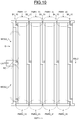
- FIGS. 10 to 12 in order to illustrate another example of design of a coupling stage EC.
- a coupling stage EC having an overall capacitive value equal to 135 fF and an overall inductive value equal to 685 pH.
- the distance between components, here for example power amplifiers AP, coupled to said coupling stage is for example 220 ⁇ m.
- the rms value of the current in the coupling stage is limited for example to 100 mA so that a minimum width for all of the metal tracks of said coupling stage EC may be determined.
- the effective overall capacitive value and the effective overall inductive value of said coupling stage EC are mainly determined by said first module MOD 1 and said second module MOD 2 of said coupling stage EC.
- said coupling stage EC illustrated in FIG. 10 comprises five branches B 1 _ 10 to B 5 _ 10 each having a group G having a first module MOD 1 coupled in series between two second modules MOD 2 .
- Each first module MOD 1 of said group G has a capacitive value of 12.9 fF and an inductive value of 8 pH
- each second module MOD 2 of said group G has a capacitive value of 17.8 fF and an inductive value of 67 pH.
- each branch of said coupling stage EC has a capacitive value of around 49 fF and an inductive value of 134 pH.
- a finer adjustment to the overall capacitive and inductive values could potentially be applied in such a manner as to adjust the central frequency of said 90° hybrid coupling stage.
- FIG. 11 illustrates schematically a wireless communications device APP, for example a cellular mobile telephone, comprising a transmission chain CT containing a first coupling stage EC 1 described hereinbefore being used as a power divider DIV, a second coupling stage EC 2 being used as a power combiner COMB, and two power amplifiers AP 1 and AP 2 respectively coupled between the first coupling stage EC 1 and the second coupling stage EC 2 .
- a wireless communications device APP for example a cellular mobile telephone, comprising a transmission chain CT containing a first coupling stage EC 1 described hereinbefore being used as a power divider DIV, a second coupling stage EC 2 being used as a power combiner COMB, and two power amplifiers AP 1 and AP 2 respectively coupled between the first coupling stage EC 1 and the second coupling stage EC 2 .
- One of the two first stage terminals BE 11 _ 1 of said first coupling stage EC 1 receives a first input signal SE 1 , for example a radiofrequency signal coming from a frequency transformation stage, and the other of the two first stage terminals BE 12 _ 1 is coupled to a load CHG 50 having a characteristic impedance of 50 ohms and being connected to ground so as to be isolated.
- the two second stage terminals BE 21 _ 1 and BE 22 _ 1 of said first coupling stage EC 1 each deliver a first output signal SS 1 and these first output signals SS 1 are phase-shifted by 90° with respect to each other.
- the two power amplifiers AP 1 and AP 2 are coupled in parallel between the two second stage terminals BE 21 _ 1 and BE 22 _ 1 of said first coupling stage EC 1 and the two second stage terminals BE 21 _ 2 and BE 22 _ 2 of said second coupling stage EC 2 , which advantageously allows the size of said device APP to be reduced.
- Said second coupling stage EC 2 receives, at its two second stage terminals BE 21 _ 2 and BE 22 _ 2 , the intermediate output signals SSI coming from the two power amplifiers AP 1 and AP 2 and delivers to one of the two first stage terminals BE 11 _ 2 a second output signal SS 2 , for example an amplified radiofrequency signal intended to be transmitted via an antenna for example.
- the other of the two first stage terminals BE 12 _ 2 of said second coupling stage EC 2 is coupled to a load CHG 50 having a characteristic impedance of 50 ohms and being connected to ground so as to be isolated.
- FIG. 12 illustrates schematically an example of a third coupling stage EC 3 used in a phase-shift device DD, incorporated for example into an apparatus APP 1 such as for example a radio frequency phase-shifter.
- one of the two second stage terminals BE 21 of said third coupling stage EC 3 receives a third input signal SE 3 and the other of the two second stage terminals BE 22 delivers a third output signal SS 3 .
- the two first stage terminals BE 11 and BE 12 are respectively coupled to first and second variable loads CV 1 and CV 2 having variable impedances and being respectively connected to ground.
- phase shift between said third input signal SE 3 and said third output signal SS 3 is adjustable by modifying the impedances of said first and second variable loads CV 1 and CV 2 .
- a coupling device comprising a coupling stage of limited size able to be used for example as a divider, combiner or else phase-shift device, and allowing a fast and easy adjustment of the dimensions and the capacitive and inductive values of said coupling stage.
- the fact that the input terminals of said stage in combiner mode and the output terminals of said stage in divider mode are situated in the same side of said coupling stage advantageously allows a parallel coupling of the components such as power amplifiers with a reduced space requirement.
- coupling stages within coupling devices disposed on a substrate of the silicon type, with a dielectric between the tracks have been described, these coupling stages may also be implemented on a printed circuit, within a packaging module or else in the air in suspended mode.
Landscapes
- Amplifiers (AREA)
Abstract
Description
Claims (9)
Applications Claiming Priority (1)
| Application Number | Priority Date | Filing Date | Title |
|---|---|---|---|
| PCT/FR2016/051794 WO2018011476A1 (en) | 2016-07-12 | 2016-07-12 | Integrated coupling device, in particular of the 90° hybrid type |
Publications (2)
| Publication Number | Publication Date |
|---|---|
| US20190245258A1 US20190245258A1 (en) | 2019-08-08 |
| US10985437B2 true US10985437B2 (en) | 2021-04-20 |
Family
ID=56738127
Family Applications (1)
| Application Number | Title | Priority Date | Filing Date |
|---|---|---|---|
| US16/317,082 Active US10985437B2 (en) | 2016-07-12 | 2016-07-12 | Integrated coupling device, in particular of the 90° hybrid type |
Country Status (2)
| Country | Link |
|---|---|
| US (1) | US10985437B2 (en) |
| WO (1) | WO2018011476A1 (en) |
Families Citing this family (1)
| Publication number | Priority date | Publication date | Assignee | Title |
|---|---|---|---|---|
| FR3151713A1 (en) * | 2023-07-27 | 2025-01-31 | Stmicroelectronics International N.V. | Ninety Degree Hybrid Coupler |
Citations (15)
| Publication number | Priority date | Publication date | Assignee | Title |
|---|---|---|---|---|
| GB896707A (en) | 1958-01-16 | 1962-05-16 | Csf | Improvements in or relating to hybrid junctions for use on very high frequencies |
| US3264586A (en) * | 1963-12-27 | 1966-08-02 | Premier Microwave Corp | Variable attenuator for u. h. f. and microwave circuits |
| US3371284A (en) * | 1964-10-30 | 1968-02-27 | Bell Telephone Labor Inc | High frequency balanced amplifier |
| US3440570A (en) * | 1967-10-12 | 1969-04-22 | Bell Telephone Labor Inc | Microwave phase shifter |
| US3737810A (en) * | 1969-05-05 | 1973-06-05 | Radiation Systems Inc | Wideband tem components |
| US4482873A (en) * | 1982-09-16 | 1984-11-13 | Rockwell International Corporation | Printed hybrid quadrature 3 dB signal coupler apparatus |
| US4532484A (en) * | 1982-11-09 | 1985-07-30 | Raytheon Company | Hybrid coupler having interlaced coupling conductors |
| US5281929A (en) * | 1992-03-05 | 1994-01-25 | Itt Corporation | Microstrip twisted broadside coupler apparatus |
| EP0669671A1 (en) | 1994-02-24 | 1995-08-30 | Hughes Aircraft Company | Cavity matched hybrid coupler |
| WO1998002141A1 (en) | 1996-07-15 | 1998-01-22 | Alza Corporation | Interlocking osmotic device |
| US20050017821A1 (en) * | 2001-11-30 | 2005-01-27 | Andrzej Sawicki | Directional coupler |
| US7190240B2 (en) * | 2003-06-25 | 2007-03-13 | Werlatone, Inc. | Multi-section coupler assembly |
| US7808343B1 (en) | 2008-10-03 | 2010-10-05 | Lockheed Martin Corporation | Radio frequency (RF) signal combiner having inverted coupler |
| US20120019335A1 (en) | 2010-07-20 | 2012-01-26 | Hoang Dinhphuoc V | Self compensated directional coupler |
| US20150293304A1 (en) * | 2014-04-15 | 2015-10-15 | Gatesair, Inc. | Directional coupler system |
Family Cites Families (2)
| Publication number | Priority date | Publication date | Assignee | Title |
|---|---|---|---|---|
| US3370284A (en) * | 1965-01-21 | 1968-02-20 | Samuel M. Bagno | Optical space alarm |
| US5907266A (en) * | 1996-11-26 | 1999-05-25 | Raytheon Company | Alignment tolerant overlay directional coupler |
-
2016
- 2016-07-12 WO PCT/FR2016/051794 patent/WO2018011476A1/en not_active Ceased
- 2016-07-12 US US16/317,082 patent/US10985437B2/en active Active
Patent Citations (15)
| Publication number | Priority date | Publication date | Assignee | Title |
|---|---|---|---|---|
| GB896707A (en) | 1958-01-16 | 1962-05-16 | Csf | Improvements in or relating to hybrid junctions for use on very high frequencies |
| US3264586A (en) * | 1963-12-27 | 1966-08-02 | Premier Microwave Corp | Variable attenuator for u. h. f. and microwave circuits |
| US3371284A (en) * | 1964-10-30 | 1968-02-27 | Bell Telephone Labor Inc | High frequency balanced amplifier |
| US3440570A (en) * | 1967-10-12 | 1969-04-22 | Bell Telephone Labor Inc | Microwave phase shifter |
| US3737810A (en) * | 1969-05-05 | 1973-06-05 | Radiation Systems Inc | Wideband tem components |
| US4482873A (en) * | 1982-09-16 | 1984-11-13 | Rockwell International Corporation | Printed hybrid quadrature 3 dB signal coupler apparatus |
| US4532484A (en) * | 1982-11-09 | 1985-07-30 | Raytheon Company | Hybrid coupler having interlaced coupling conductors |
| US5281929A (en) * | 1992-03-05 | 1994-01-25 | Itt Corporation | Microstrip twisted broadside coupler apparatus |
| EP0669671A1 (en) | 1994-02-24 | 1995-08-30 | Hughes Aircraft Company | Cavity matched hybrid coupler |
| WO1998002141A1 (en) | 1996-07-15 | 1998-01-22 | Alza Corporation | Interlocking osmotic device |
| US20050017821A1 (en) * | 2001-11-30 | 2005-01-27 | Andrzej Sawicki | Directional coupler |
| US7190240B2 (en) * | 2003-06-25 | 2007-03-13 | Werlatone, Inc. | Multi-section coupler assembly |
| US7808343B1 (en) | 2008-10-03 | 2010-10-05 | Lockheed Martin Corporation | Radio frequency (RF) signal combiner having inverted coupler |
| US20120019335A1 (en) | 2010-07-20 | 2012-01-26 | Hoang Dinhphuoc V | Self compensated directional coupler |
| US20150293304A1 (en) * | 2014-04-15 | 2015-10-15 | Gatesair, Inc. | Directional coupler system |
Non-Patent Citations (1)
| Title |
|---|
| International Search Report and Written Opinion for PCT/FR2016/051794 dated Mar. 23, 2017 (11 pages). |
Also Published As
| Publication number | Publication date |
|---|---|
| US20190245258A1 (en) | 2019-08-08 |
| WO2018011476A1 (en) | 2018-01-18 |
Similar Documents
| Publication | Publication Date | Title |
|---|---|---|
| EP3093987B1 (en) | Phase correction in a doherty power amplifier | |
| CN104218901B (en) | Radio frequency transmitter and power combiner | |
| US9136580B2 (en) | Quadrature hybrid coupler, amplifier, and wireless communication device | |
| US9461695B2 (en) | Semiconductor device including spiral-shape inductor and horseshoe-shape inductor | |
| CN108336971B (en) | Power amplifying module | |
| EP2843832A1 (en) | A wideband amplifier | |
| US9281888B1 (en) | Quadrature signal generator, beamforming arrangement, communication device and base station | |
| JP2013085179A (en) | Power amplification circuit and radio communication apparatus | |
| KR20130123305A (en) | Doherty amplifier | |
| CN108141179A (en) | Power amplifier | |
| CN104009787B (en) | Transmitting device and for analyze amplification transmission signal method | |
| US8779826B1 (en) | Power splitter and combiner | |
| US20230086793A1 (en) | Radio frequency module and communication device | |
| US10985437B2 (en) | Integrated coupling device, in particular of the 90° hybrid type | |
| WO2023017760A1 (en) | High-frequency circuit, communication device, and power amplification method for high-frequency circuit | |
| EP2779470B1 (en) | Integrated circuit for transmitting and receiving an RF signal | |
| JP2018133812A (en) | High-frequency front end circuit | |
| US12388162B2 (en) | Marchand balun formed in a laminated substrate and including a main line and sub-lines, where a parallel line is connected to a sub-line | |
| US12597898B2 (en) | High-frequency circuit and communication device | |
| US20230036397A1 (en) | Balun | |
| US11916529B2 (en) | Matching circuit | |
| US11335493B2 (en) | Integrated transformer | |
| US12609664B2 (en) | Radio-frequency module and communication device | |
| US12230859B2 (en) | Balun | |
| TW201517379A (en) | Antenna tuner |
Legal Events
| Date | Code | Title | Description |
|---|---|---|---|
| AS | Assignment |
Owner name: STMICROELECTRONICS SA, FRANCE Free format text: ASSIGNMENT OF ASSIGNORS INTEREST;ASSIGNORS:KNOPIK, VINCENT;MORET, BORIS;KERHERVE, ERIC;SIGNING DATES FROM 20181121 TO 20181126;REEL/FRAME:047963/0427 |
|
| FEPP | Fee payment procedure |
Free format text: ENTITY STATUS SET TO UNDISCOUNTED (ORIGINAL EVENT CODE: BIG.); ENTITY STATUS OF PATENT OWNER: LARGE ENTITY |
|
| STPP | Information on status: patent application and granting procedure in general |
Free format text: DOCKETED NEW CASE - READY FOR EXAMINATION |
|
| STPP | Information on status: patent application and granting procedure in general |
Free format text: NON FINAL ACTION MAILED |
|
| STPP | Information on status: patent application and granting procedure in general |
Free format text: RESPONSE TO NON-FINAL OFFICE ACTION ENTERED AND FORWARDED TO EXAMINER |
|
| STPP | Information on status: patent application and granting procedure in general |
Free format text: NOTICE OF ALLOWANCE MAILED -- APPLICATION RECEIVED IN OFFICE OF PUBLICATIONS |
|
| STPP | Information on status: patent application and granting procedure in general |
Free format text: NOTICE OF ALLOWANCE MAILED -- APPLICATION RECEIVED IN OFFICE OF PUBLICATIONS |
|
| STPP | Information on status: patent application and granting procedure in general |
Free format text: PUBLICATIONS -- ISSUE FEE PAYMENT VERIFIED |
|
| STCF | Information on status: patent grant |
Free format text: PATENTED CASE |
|
| AS | Assignment |
Owner name: STMICROELECTRONICS FRANCE, FRANCE Free format text: CHANGE OF NAME;ASSIGNOR:STMICROELECTRONICS SA;REEL/FRAME:066663/0136 Effective date: 20230126 |
|
| MAFP | Maintenance fee payment |
Free format text: PAYMENT OF MAINTENANCE FEE, 4TH YEAR, LARGE ENTITY (ORIGINAL EVENT CODE: M1551); ENTITY STATUS OF PATENT OWNER: LARGE ENTITY Year of fee payment: 4 |