US10985327B2 - Microcrystalline organic semiconductor film, organic semiconductor transistor, and method of manufacturing organic semiconductor transistor - Google Patents
Microcrystalline organic semiconductor film, organic semiconductor transistor, and method of manufacturing organic semiconductor transistor Download PDFInfo
- Publication number
- US10985327B2 US10985327B2 US16/358,910 US201916358910A US10985327B2 US 10985327 B2 US10985327 B2 US 10985327B2 US 201916358910 A US201916358910 A US 201916358910A US 10985327 B2 US10985327 B2 US 10985327B2
- Authority
- US
- United States
- Prior art keywords
- group
- organic semiconductor
- atom
- carbon atoms
- formula
- Prior art date
- Legal status (The legal status is an assumption and is not a legal conclusion. Google has not performed a legal analysis and makes no representation as to the accuracy of the status listed.)
- Active, expires
Links
- 239000004065 semiconductor Substances 0.000 title claims description 328
- 238000004519 manufacturing process Methods 0.000 title claims description 116
- 125000000217 alkyl group Chemical group 0.000 claims abstract description 52
- 125000003118 aryl group Chemical group 0.000 claims abstract description 47
- 125000001072 heteroaryl group Chemical group 0.000 claims abstract description 39
- 125000004429 atom Chemical group 0.000 claims abstract description 31
- 125000003342 alkenyl group Chemical group 0.000 claims abstract description 28
- 125000000304 alkynyl group Chemical group 0.000 claims abstract description 27
- 125000004435 hydrogen atom Chemical group [H]* 0.000 claims abstract description 21
- 125000005843 halogen group Chemical group 0.000 claims abstract description 9
- 150000001875 compounds Chemical class 0.000 claims description 130
- 125000004432 carbon atom Chemical group C* 0.000 claims description 129
- 229910052717 sulfur Inorganic materials 0.000 claims description 64
- 125000004434 sulfur atom Chemical group 0.000 claims description 64
- 239000013078 crystal Substances 0.000 claims description 47
- 125000004430 oxygen atom Chemical group O* 0.000 claims description 38
- 125000001424 substituent group Chemical group 0.000 claims description 36
- BUGBHKTXTAQXES-UHFFFAOYSA-N Selenium Chemical group [Se] BUGBHKTXTAQXES-UHFFFAOYSA-N 0.000 claims description 25
- 229910052711 selenium Inorganic materials 0.000 claims description 25
- 238000000059 patterning Methods 0.000 claims description 18
- 125000001931 aliphatic group Chemical group 0.000 claims description 14
- YLQBMQCUIZJEEH-UHFFFAOYSA-N Furan Chemical group C=1C=COC=1 YLQBMQCUIZJEEH-UHFFFAOYSA-N 0.000 claims description 11
- 229910052757 nitrogen Inorganic materials 0.000 claims description 9
- 125000004433 nitrogen atom Chemical group N* 0.000 claims description 9
- 238000000151 deposition Methods 0.000 claims description 8
- 125000001997 phenyl group Chemical group [H]C1=C([H])C([H])=C(*)C([H])=C1[H] 0.000 claims description 8
- 125000002883 imidazolyl group Chemical group 0.000 claims description 7
- 229910052714 tellurium Inorganic materials 0.000 claims description 6
- PORWMNRCUJJQNO-UHFFFAOYSA-N tellurium atom Chemical group [Te] PORWMNRCUJJQNO-UHFFFAOYSA-N 0.000 claims description 6
- YTPLMLYBLZKORZ-UHFFFAOYSA-N Thiophene Chemical group C=1C=CSC=1 YTPLMLYBLZKORZ-UHFFFAOYSA-N 0.000 claims description 5
- 125000000168 pyrrolyl group Chemical group 0.000 claims description 5
- MABNMNVCOAICNO-UHFFFAOYSA-N selenophene Chemical group C=1C=C[se]C=1 MABNMNVCOAICNO-UHFFFAOYSA-N 0.000 claims description 5
- FZWLAAWBMGSTSO-UHFFFAOYSA-N Thiazole Chemical group C1=CSC=N1 FZWLAAWBMGSTSO-UHFFFAOYSA-N 0.000 claims description 3
- 125000002971 oxazolyl group Chemical group 0.000 claims description 3
- OTMSDBZUPAUEDD-UHFFFAOYSA-N CC Chemical compound CC OTMSDBZUPAUEDD-UHFFFAOYSA-N 0.000 description 770
- YXFVVABEGXRONW-UHFFFAOYSA-N Toluene Chemical compound CC1=CC=CC=C1 YXFVVABEGXRONW-UHFFFAOYSA-N 0.000 description 154
- 239000010408 film Substances 0.000 description 132
- 239000010410 layer Substances 0.000 description 122
- 230000037230 mobility Effects 0.000 description 109
- 0 CC.CC.[1*]c1cc2#c([y]1)C=C1C(=C2)C/C2=C/c3cc([2*])[y]c#3/C=C\12 Chemical compound CC.CC.[1*]c1cc2#c([y]1)C=C1C(=C2)C/C2=C/c3cc([2*])[y]c#3/C=C\12 0.000 description 71
- VLKZOEOYAKHREP-UHFFFAOYSA-N n-Hexane Chemical compound CCCCCC VLKZOEOYAKHREP-UHFFFAOYSA-N 0.000 description 69
- 230000000052 comparative effect Effects 0.000 description 63
- QCWXDVFBZVHKLV-UHFFFAOYSA-N CC1=CC=C(C(C)(C)C)C=C1 Chemical compound CC1=CC=C(C(C)(C)C)C=C1 QCWXDVFBZVHKLV-UHFFFAOYSA-N 0.000 description 62
- QMMFVYPAHWMCMS-UHFFFAOYSA-N CSC Chemical compound CSC QMMFVYPAHWMCMS-UHFFFAOYSA-N 0.000 description 58
- LCGLNKUTAGEVQW-UHFFFAOYSA-N COC Chemical compound COC LCGLNKUTAGEVQW-UHFFFAOYSA-N 0.000 description 54
- VNWKTOKETHGBQD-UHFFFAOYSA-N [H]C Chemical compound [H]C VNWKTOKETHGBQD-UHFFFAOYSA-N 0.000 description 52
- 238000000034 method Methods 0.000 description 49
- ZWEHNKRNPOVVGH-UHFFFAOYSA-N CCC(C)=O Chemical compound CCC(C)=O ZWEHNKRNPOVVGH-UHFFFAOYSA-N 0.000 description 43
- 239000000243 solution Substances 0.000 description 41
- YBJCDTIWNDBNTM-UHFFFAOYSA-N CCS(C)(=O)=O Chemical compound CCS(C)(=O)=O YBJCDTIWNDBNTM-UHFFFAOYSA-N 0.000 description 37
- 230000015572 biosynthetic process Effects 0.000 description 32
- 239000000758 substrate Substances 0.000 description 32
- 238000011156 evaluation Methods 0.000 description 29
- BBDGYADAMYMJNO-UHFFFAOYSA-N CCCCN(CC)CCCC Chemical compound CCCCN(CC)CCCC BBDGYADAMYMJNO-UHFFFAOYSA-N 0.000 description 27
- XNMQEEKYCVKGBD-UHFFFAOYSA-N CC#CC Chemical compound CC#CC XNMQEEKYCVKGBD-UHFFFAOYSA-N 0.000 description 22
- 125000001280 n-hexyl group Chemical group C(CCCCC)* 0.000 description 21
- WXEHBUMAEPOYKP-UHFFFAOYSA-N CCSC Chemical compound CCSC WXEHBUMAEPOYKP-UHFFFAOYSA-N 0.000 description 20
- RYPKRALMXUUNKS-UHFFFAOYSA-N CC=CCCC Chemical compound CC=CCCC RYPKRALMXUUNKS-UHFFFAOYSA-N 0.000 description 18
- 125000001449 isopropyl group Chemical group [H]C([H])([H])C([H])(*)C([H])([H])[H] 0.000 description 18
- -1 p-pentylphenyl group Chemical group 0.000 description 18
- WYURNTSHIVDZCO-UHFFFAOYSA-N Tetrahydrofuran Chemical compound C1CCOC1 WYURNTSHIVDZCO-UHFFFAOYSA-N 0.000 description 16
- ZMDAEGAYOCVWRS-UHFFFAOYSA-N CC1=CC=C(C(C)C)S1 Chemical compound CC1=CC=C(C(C)C)S1 ZMDAEGAYOCVWRS-UHFFFAOYSA-N 0.000 description 15
- RTZKZFJDLAIYFH-UHFFFAOYSA-N Diethyl ether Chemical compound CCOCC RTZKZFJDLAIYFH-UHFFFAOYSA-N 0.000 description 15
- VTRRCXRVEQTTOE-UHFFFAOYSA-N CCS(C)=O Chemical compound CCS(C)=O VTRRCXRVEQTTOE-UHFFFAOYSA-N 0.000 description 14
- VYPSYNLAJGMNEJ-UHFFFAOYSA-N Silicium dioxide Chemical compound O=[Si]=O VYPSYNLAJGMNEJ-UHFFFAOYSA-N 0.000 description 14
- 229920000620 organic polymer Polymers 0.000 description 13
- 238000007789 sealing Methods 0.000 description 13
- 238000003786 synthesis reaction Methods 0.000 description 13
- HEDRZPFGACZZDS-MICDWDOJSA-N Trichloro(2H)methane Chemical compound [2H]C(Cl)(Cl)Cl HEDRZPFGACZZDS-MICDWDOJSA-N 0.000 description 12
- 238000000576 coating method Methods 0.000 description 12
- AFABGHUZZDYHJO-UHFFFAOYSA-N CCCC(C)C Chemical compound CCCC(C)C AFABGHUZZDYHJO-UHFFFAOYSA-N 0.000 description 11
- ZYVYEJXMYBUCMN-UHFFFAOYSA-N COCC(C)C Chemical compound COCC(C)C ZYVYEJXMYBUCMN-UHFFFAOYSA-N 0.000 description 11
- 229940125904 compound 1 Drugs 0.000 description 11
- BFIMMTCNYPIMRN-UHFFFAOYSA-N CC1=CC(C)=C(C)C(C)=C1 Chemical compound CC1=CC(C)=C(C)C(C)=C1 BFIMMTCNYPIMRN-UHFFFAOYSA-N 0.000 description 10
- SIEMKBNGGJTDME-UHFFFAOYSA-N CC1=CC2=C(N=C(C)S2)S1 Chemical compound CC1=CC2=C(N=C(C)S2)S1 SIEMKBNGGJTDME-UHFFFAOYSA-N 0.000 description 10
- LRLRAYMYEXQKID-UHFFFAOYSA-N CC1=CC=C(C(F)(F)F)C=C1 Chemical compound CC1=CC=C(C(F)(F)F)C=C1 LRLRAYMYEXQKID-UHFFFAOYSA-N 0.000 description 10
- AOSOZARHUJMBLZ-UHFFFAOYSA-N CC1=CN=C(F)C=C1 Chemical compound CC1=CN=C(F)C=C1 AOSOZARHUJMBLZ-UHFFFAOYSA-N 0.000 description 10
- UAEPNZWRGJTJPN-UHFFFAOYSA-N CC1CCCCC1 Chemical compound CC1CCCCC1 UAEPNZWRGJTJPN-UHFFFAOYSA-N 0.000 description 10
- PFEOZHBOMNWTJB-UHFFFAOYSA-N CCC(C)CC Chemical compound CCC(C)CC PFEOZHBOMNWTJB-UHFFFAOYSA-N 0.000 description 10
- XOBKSJJDNFUZPF-UHFFFAOYSA-N CCOC Chemical compound CCOC XOBKSJJDNFUZPF-UHFFFAOYSA-N 0.000 description 10
- 239000011669 selenium Substances 0.000 description 10
- URLKBWYHVLBVBO-UHFFFAOYSA-N CC1=CC=C(C)C=C1 Chemical compound CC1=CC=C(C)C=C1 URLKBWYHVLBVBO-UHFFFAOYSA-N 0.000 description 8
- FUHSVKSNUCZRQQ-UHFFFAOYSA-N CCC1=CC2=CC(C)=CC=C2S1 Chemical compound CCC1=CC2=CC(C)=CC=C2S1 FUHSVKSNUCZRQQ-UHFFFAOYSA-N 0.000 description 8
- YMWUJEATGCHHMB-UHFFFAOYSA-N Dichloromethane Chemical compound ClCCl YMWUJEATGCHHMB-UHFFFAOYSA-N 0.000 description 8
- CSNNHWWHGAXBCP-UHFFFAOYSA-L Magnesium sulfate Chemical compound [Mg+2].[O-][S+2]([O-])([O-])[O-] CSNNHWWHGAXBCP-UHFFFAOYSA-L 0.000 description 8
- ZMXDDKWLCZADIW-UHFFFAOYSA-N N,N-Dimethylformamide Chemical compound CN(C)C=O ZMXDDKWLCZADIW-UHFFFAOYSA-N 0.000 description 8
- XUIMIQQOPSSXEZ-UHFFFAOYSA-N Silicon Chemical compound [Si] XUIMIQQOPSSXEZ-UHFFFAOYSA-N 0.000 description 8
- 238000006243 chemical reaction Methods 0.000 description 8
- 239000011248 coating agent Substances 0.000 description 8
- 229910052710 silicon Inorganic materials 0.000 description 8
- 239000010703 silicon Substances 0.000 description 8
- 239000013077 target material Substances 0.000 description 8
- DEXFNLNNUZKHNO-UHFFFAOYSA-N 6-[3-[4-[2-(2,3-dihydro-1H-inden-2-ylamino)pyrimidin-5-yl]piperidin-1-yl]-3-oxopropyl]-3H-1,3-benzoxazol-2-one Chemical compound C1C(CC2=CC=CC=C12)NC1=NC=C(C=N1)C1CCN(CC1)C(CCC1=CC2=C(NC(O2)=O)C=C1)=O DEXFNLNNUZKHNO-UHFFFAOYSA-N 0.000 description 7
- 239000002253 acid Substances 0.000 description 7
- 125000000623 heterocyclic group Chemical group 0.000 description 7
- 229910052809 inorganic oxide Inorganic materials 0.000 description 7
- 238000007639 printing Methods 0.000 description 7
- 238000007740 vapor deposition Methods 0.000 description 7
- 238000005160 1H NMR spectroscopy Methods 0.000 description 6
- ATUOYWHBWRKTHZ-UHFFFAOYSA-N CCC Chemical compound CCC ATUOYWHBWRKTHZ-UHFFFAOYSA-N 0.000 description 6
- XEKOWRVHYACXOJ-UHFFFAOYSA-N Ethyl acetate Chemical compound CCOC(C)=O XEKOWRVHYACXOJ-UHFFFAOYSA-N 0.000 description 6
- OKKJLVBELUTLKV-UHFFFAOYSA-N Methanol Chemical compound OC OKKJLVBELUTLKV-UHFFFAOYSA-N 0.000 description 6
- MZRVEZGGRBJDDB-UHFFFAOYSA-N N-Butyllithium Chemical compound [Li]CCCC MZRVEZGGRBJDDB-UHFFFAOYSA-N 0.000 description 6
- 125000000753 cycloalkyl group Chemical group 0.000 description 6
- 230000002950 deficient Effects 0.000 description 6
- 239000011521 glass Substances 0.000 description 6
- 239000010931 gold Substances 0.000 description 6
- 239000000047 product Substances 0.000 description 6
- YRABRACUKBOTKB-UHFFFAOYSA-N CC1=CC=C(C)N1C Chemical compound CC1=CC=C(C)N1C YRABRACUKBOTKB-UHFFFAOYSA-N 0.000 description 5
- GSNUFIFRDBKVIE-UHFFFAOYSA-N CC1=CC=C(C)O1 Chemical compound CC1=CC=C(C)O1 GSNUFIFRDBKVIE-UHFFFAOYSA-N 0.000 description 5
- ZZLCFHIKESPLTH-UHFFFAOYSA-N CC1=CC=C(C2=CC=CC=C2)C=C1 Chemical compound CC1=CC=C(C2=CC=CC=C2)C=C1 ZZLCFHIKESPLTH-UHFFFAOYSA-N 0.000 description 5
- WVUHHPQQQLBMOE-UHFFFAOYSA-N CC1=CN=C(C)S1 Chemical compound CC1=CN=C(C)S1 WVUHHPQQQLBMOE-UHFFFAOYSA-N 0.000 description 5
- XSTRMLBPCRZKMJ-UHFFFAOYSA-N CC=C(CCC)CCC Chemical compound CC=C(CCC)CCC XSTRMLBPCRZKMJ-UHFFFAOYSA-N 0.000 description 5
- IJDNQMDRQITEOD-UHFFFAOYSA-N CCCC Chemical compound CCCC IJDNQMDRQITEOD-UHFFFAOYSA-N 0.000 description 5
- OFBQJSOFQDEBGM-UHFFFAOYSA-N CCCCC Chemical compound CCCCC OFBQJSOFQDEBGM-UHFFFAOYSA-N 0.000 description 5
- DUVLJBQCIZCUMW-UHFFFAOYSA-N CCS(=O)C1=CC=CC=C1 Chemical compound CCS(=O)C1=CC=CC=C1 DUVLJBQCIZCUMW-UHFFFAOYSA-N 0.000 description 5
- 229910052681 coesite Inorganic materials 0.000 description 5
- 229910052906 cristobalite Inorganic materials 0.000 description 5
- 229960004132 diethyl ether Drugs 0.000 description 5
- 239000007772 electrode material Substances 0.000 description 5
- 239000000463 material Substances 0.000 description 5
- 229910052751 metal Inorganic materials 0.000 description 5
- 239000002184 metal Substances 0.000 description 5
- AICOOMRHRUFYCM-ZRRPKQBOSA-N oxazine, 1 Chemical compound C([C@@H]1[C@H](C(C[C@]2(C)[C@@H]([C@H](C)N(C)C)[C@H](O)C[C@]21C)=O)CC1=CC2)C[C@H]1[C@@]1(C)[C@H]2N=C(C(C)C)OC1 AICOOMRHRUFYCM-ZRRPKQBOSA-N 0.000 description 5
- 150000003254 radicals Chemical class 0.000 description 5
- 239000000377 silicon dioxide Substances 0.000 description 5
- 229910052682 stishovite Inorganic materials 0.000 description 5
- 229910052905 tridymite Inorganic materials 0.000 description 5
- XLYOFNOQVPJJNP-UHFFFAOYSA-N water Substances O XLYOFNOQVPJJNP-UHFFFAOYSA-N 0.000 description 5
- VZSRBBMJRBPUNF-UHFFFAOYSA-N 2-(2,3-dihydro-1H-inden-2-ylamino)-N-[3-oxo-3-(2,4,6,7-tetrahydrotriazolo[4,5-c]pyridin-5-yl)propyl]pyrimidine-5-carboxamide Chemical compound C1C(CC2=CC=CC=C12)NC1=NC=C(C=N1)C(=O)NCCC(N1CC2=C(CC1)NN=N2)=O VZSRBBMJRBPUNF-UHFFFAOYSA-N 0.000 description 4
- XXDVDCUHNQCYPE-UHFFFAOYSA-N CC1=CC=C(C(C)C)N1C Chemical compound CC1=CC=C(C(C)C)N1C XXDVDCUHNQCYPE-UHFFFAOYSA-N 0.000 description 4
- WQEMAMKFYWGSNI-UHFFFAOYSA-N CC1=CC=C(Cl)N1C Chemical compound CC1=CC=C(Cl)N1C WQEMAMKFYWGSNI-UHFFFAOYSA-N 0.000 description 4
- LNJMHEJAYSYZKK-UHFFFAOYSA-N CC1=NC=CC=N1 Chemical compound CC1=NC=CC=N1 LNJMHEJAYSYZKK-UHFFFAOYSA-N 0.000 description 4
- 229940126062 Compound A Drugs 0.000 description 4
- NLDMNSXOCDLTTB-UHFFFAOYSA-N Heterophylliin A Natural products O1C2COC(=O)C3=CC(O)=C(O)C(O)=C3C3=C(O)C(O)=C(O)C=C3C(=O)OC2C(OC(=O)C=2C=C(O)C(O)=C(O)C=2)C(O)C1OC(=O)C1=CC(O)=C(O)C(O)=C1 NLDMNSXOCDLTTB-UHFFFAOYSA-N 0.000 description 4
- 238000004458 analytical method Methods 0.000 description 4
- RDOXTESZEPMUJZ-UHFFFAOYSA-N anisole Chemical compound COC1=CC=CC=C1 RDOXTESZEPMUJZ-UHFFFAOYSA-N 0.000 description 4
- 125000000751 azo group Chemical group [*]N=N[*] 0.000 description 4
- 125000006841 cyclic skeleton Chemical group 0.000 description 4
- 230000000694 effects Effects 0.000 description 4
- 229910052731 fluorine Inorganic materials 0.000 description 4
- 125000001153 fluoro group Chemical group F* 0.000 description 4
- 229910052943 magnesium sulfate Inorganic materials 0.000 description 4
- 235000019341 magnesium sulphate Nutrition 0.000 description 4
- 239000000203 mixture Substances 0.000 description 4
- 239000012044 organic layer Substances 0.000 description 4
- 239000003505 polymerization initiator Substances 0.000 description 4
- 229910052814 silicon oxide Inorganic materials 0.000 description 4
- 239000010409 thin film Substances 0.000 description 4
- 238000001771 vacuum deposition Methods 0.000 description 4
- HMUNWXXNJPVALC-UHFFFAOYSA-N 1-[4-[2-(2,3-dihydro-1H-inden-2-ylamino)pyrimidin-5-yl]piperazin-1-yl]-2-(2,4,6,7-tetrahydrotriazolo[4,5-c]pyridin-5-yl)ethanone Chemical compound C1C(CC2=CC=CC=C12)NC1=NC=C(C=N1)N1CCN(CC1)C(CN1CC2=C(CC1)NN=N2)=O HMUNWXXNJPVALC-UHFFFAOYSA-N 0.000 description 3
- VYZAMTAEIAYCRO-UHFFFAOYSA-N Chromium Chemical compound [Cr] VYZAMTAEIAYCRO-UHFFFAOYSA-N 0.000 description 3
- KWYUFKZDYYNOTN-UHFFFAOYSA-M Potassium hydroxide Chemical compound [OH-].[K+] KWYUFKZDYYNOTN-UHFFFAOYSA-M 0.000 description 3
- HEMHJVSKTPXQMS-UHFFFAOYSA-M Sodium hydroxide Chemical compound [OH-].[Na+] HEMHJVSKTPXQMS-UHFFFAOYSA-M 0.000 description 3
- 150000001491 aromatic compounds Chemical class 0.000 description 3
- 229910052801 chlorine Inorganic materials 0.000 description 3
- 125000001309 chloro group Chemical group Cl* 0.000 description 3
- 229910052804 chromium Inorganic materials 0.000 description 3
- 239000011651 chromium Substances 0.000 description 3
- 238000004440 column chromatography Methods 0.000 description 3
- 238000004132 cross linking Methods 0.000 description 3
- 125000004122 cyclic group Chemical group 0.000 description 3
- 230000006866 deterioration Effects 0.000 description 3
- 238000010304 firing Methods 0.000 description 3
- 230000006870 function Effects 0.000 description 3
- PCHJSUWPFVWCPO-UHFFFAOYSA-N gold Chemical compound [Au] PCHJSUWPFVWCPO-UHFFFAOYSA-N 0.000 description 3
- 229910052737 gold Inorganic materials 0.000 description 3
- 238000010438 heat treatment Methods 0.000 description 3
- 238000011835 investigation Methods 0.000 description 3
- 229920003023 plastic Polymers 0.000 description 3
- 239000004033 plastic Substances 0.000 description 3
- 229920001343 polytetrafluoroethylene Polymers 0.000 description 3
- 239000004810 polytetrafluoroethylene Substances 0.000 description 3
- 229920005989 resin Polymers 0.000 description 3
- 239000011347 resin Substances 0.000 description 3
- 229910052709 silver Inorganic materials 0.000 description 3
- 239000004332 silver Substances 0.000 description 3
- 125000003808 silyl group Chemical group [H][Si]([H])([H])[*] 0.000 description 3
- 239000007787 solid Substances 0.000 description 3
- 239000002904 solvent Substances 0.000 description 3
- 238000004544 sputter deposition Methods 0.000 description 3
- 239000000126 substance Substances 0.000 description 3
- 238000004381 surface treatment Methods 0.000 description 3
- CXWXQJXEFPUFDZ-UHFFFAOYSA-N tetralin Chemical compound C1=CC=C2CCCCC2=C1 CXWXQJXEFPUFDZ-UHFFFAOYSA-N 0.000 description 3
- 125000001544 thienyl group Chemical group 0.000 description 3
- JIAARYAFYJHUJI-UHFFFAOYSA-L zinc dichloride Chemical compound [Cl-].[Cl-].[Zn+2] JIAARYAFYJHUJI-UHFFFAOYSA-L 0.000 description 3
- KZPYGQFFRCFCPP-UHFFFAOYSA-N 1,1'-bis(diphenylphosphino)ferrocene Chemical compound [Fe+2].C1=CC=C[C-]1P(C=1C=CC=CC=1)C1=CC=CC=C1.C1=CC=C[C-]1P(C=1C=CC=CC=1)C1=CC=CC=C1 KZPYGQFFRCFCPP-UHFFFAOYSA-N 0.000 description 2
- RKMGAJGJIURJSJ-UHFFFAOYSA-N 2,2,6,6-Tetramethylpiperidine Substances CC1(C)CCCC(C)(C)N1 RKMGAJGJIURJSJ-UHFFFAOYSA-N 0.000 description 2
- WZFUQSJFWNHZHM-UHFFFAOYSA-N 2-[4-[2-(2,3-dihydro-1H-inden-2-ylamino)pyrimidin-5-yl]piperazin-1-yl]-1-(2,4,6,7-tetrahydrotriazolo[4,5-c]pyridin-5-yl)ethanone Chemical compound C1C(CC2=CC=CC=C12)NC1=NC=C(C=N1)N1CCN(CC1)CC(=O)N1CC2=C(CC1)NN=N2 WZFUQSJFWNHZHM-UHFFFAOYSA-N 0.000 description 2
- ZCYVEMRRCGMTRW-UHFFFAOYSA-N 7553-56-2 Chemical group [I] ZCYVEMRRCGMTRW-UHFFFAOYSA-N 0.000 description 2
- KZMGYPLQYOPHEL-UHFFFAOYSA-N Boron trifluoride etherate Chemical compound FB(F)F.CCOCC KZMGYPLQYOPHEL-UHFFFAOYSA-N 0.000 description 2
- WKBOTKDWSSQWDR-UHFFFAOYSA-N Bromine atom Chemical group [Br] WKBOTKDWSSQWDR-UHFFFAOYSA-N 0.000 description 2
- NNPPMTNAJDCUHE-UHFFFAOYSA-N CC(C)C Chemical compound CC(C)C NNPPMTNAJDCUHE-UHFFFAOYSA-N 0.000 description 2
- NEHMKBQYUWJMIP-UHFFFAOYSA-N CCl Chemical compound CCl NEHMKBQYUWJMIP-UHFFFAOYSA-N 0.000 description 2
- NBVXSUQYWXRMNV-UHFFFAOYSA-N CF Chemical compound CF NBVXSUQYWXRMNV-UHFFFAOYSA-N 0.000 description 2
- OKTJSMMVPCPJKN-UHFFFAOYSA-N Carbon Chemical compound [C] OKTJSMMVPCPJKN-UHFFFAOYSA-N 0.000 description 2
- HEDRZPFGACZZDS-UHFFFAOYSA-N Chloroform Chemical compound ClC(Cl)Cl HEDRZPFGACZZDS-UHFFFAOYSA-N 0.000 description 2
- VEXZGXHMUGYJMC-UHFFFAOYSA-N Hydrochloric acid Chemical compound Cl VEXZGXHMUGYJMC-UHFFFAOYSA-N 0.000 description 2
- PXHVJJICTQNCMI-UHFFFAOYSA-N Nickel Chemical compound [Ni] PXHVJJICTQNCMI-UHFFFAOYSA-N 0.000 description 2
- 239000002033 PVDF binder Substances 0.000 description 2
- 239000004642 Polyimide Substances 0.000 description 2
- 229910052581 Si3N4 Inorganic materials 0.000 description 2
- QAOWNCQODCNURD-UHFFFAOYSA-N Sulfuric acid Chemical compound OS(O)(=O)=O QAOWNCQODCNURD-UHFFFAOYSA-N 0.000 description 2
- 238000002441 X-ray diffraction Methods 0.000 description 2
- 125000002015 acyclic group Chemical group 0.000 description 2
- 125000002252 acyl group Chemical group 0.000 description 2
- 125000004442 acylamino group Chemical group 0.000 description 2
- 125000004423 acyloxy group Chemical group 0.000 description 2
- 125000003545 alkoxy group Chemical group 0.000 description 2
- 125000004453 alkoxycarbonyl group Chemical group 0.000 description 2
- 125000004466 alkoxycarbonylamino group Chemical group 0.000 description 2
- 125000004644 alkyl sulfinyl group Chemical group 0.000 description 2
- 125000004390 alkyl sulfonyl group Chemical group 0.000 description 2
- 125000004656 alkyl sulfonylamino group Chemical group 0.000 description 2
- 125000004414 alkyl thio group Chemical group 0.000 description 2
- 229910052782 aluminium Inorganic materials 0.000 description 2
- XAGFODPZIPBFFR-UHFFFAOYSA-N aluminium Chemical compound [Al] XAGFODPZIPBFFR-UHFFFAOYSA-N 0.000 description 2
- 125000003277 amino group Chemical group 0.000 description 2
- 125000006598 aminocarbonylamino group Chemical group 0.000 description 2
- 125000004397 aminosulfonyl group Chemical group NS(=O)(=O)* 0.000 description 2
- 125000005162 aryl oxy carbonyl amino group Chemical group 0.000 description 2
- 125000005161 aryl oxy carbonyl group Chemical group 0.000 description 2
- 125000005135 aryl sulfinyl group Chemical group 0.000 description 2
- 125000004657 aryl sulfonyl amino group Chemical group 0.000 description 2
- 125000004391 aryl sulfonyl group Chemical group 0.000 description 2
- 125000005110 aryl thio group Chemical group 0.000 description 2
- 125000004104 aryloxy group Chemical group 0.000 description 2
- 239000005388 borosilicate glass Substances 0.000 description 2
- 125000000484 butyl group Chemical group [H]C([*])([H])C([H])([H])C([H])([H])C([H])([H])[H] 0.000 description 2
- 125000003917 carbamoyl group Chemical group [H]N([H])C(*)=O 0.000 description 2
- 238000005266 casting Methods 0.000 description 2
- 239000003054 catalyst Substances 0.000 description 2
- 238000005229 chemical vapour deposition Methods 0.000 description 2
- 229940125782 compound 2 Drugs 0.000 description 2
- 229940126214 compound 3 Drugs 0.000 description 2
- 239000003431 cross linking reagent Substances 0.000 description 2
- 238000010586 diagram Methods 0.000 description 2
- 239000004205 dimethyl polysiloxane Substances 0.000 description 2
- 238000005530 etching Methods 0.000 description 2
- 125000002541 furyl group Chemical group 0.000 description 2
- 125000005842 heteroatom Chemical group 0.000 description 2
- 238000002347 injection Methods 0.000 description 2
- 239000007924 injection Substances 0.000 description 2
- 239000011810 insulating material Substances 0.000 description 2
- 230000010354 integration Effects 0.000 description 2
- 229910052740 iodine Inorganic materials 0.000 description 2
- 150000002500 ions Chemical class 0.000 description 2
- 238000005259 measurement Methods 0.000 description 2
- UZKWTJUDCOPSNM-UHFFFAOYSA-N methoxybenzene Substances CCCCOC=C UZKWTJUDCOPSNM-UHFFFAOYSA-N 0.000 description 2
- 230000003287 optical effect Effects 0.000 description 2
- 239000011368 organic material Substances 0.000 description 2
- 125000001820 oxy group Chemical group [*:1]O[*:2] 0.000 description 2
- BASFCYQUMIYNBI-UHFFFAOYSA-N platinum Chemical compound [Pt] BASFCYQUMIYNBI-UHFFFAOYSA-N 0.000 description 2
- 229920000435 poly(dimethylsiloxane) Polymers 0.000 description 2
- 125000003367 polycyclic group Chemical group 0.000 description 2
- 229920001721 polyimide Polymers 0.000 description 2
- 229920000642 polymer Polymers 0.000 description 2
- 229920002981 polyvinylidene fluoride Polymers 0.000 description 2
- 150000003839 salts Chemical class 0.000 description 2
- 239000005368 silicate glass Substances 0.000 description 2
- HQVNEWCFYHHQES-UHFFFAOYSA-N silicon nitride Chemical compound N12[Si]34N5[Si]62N3[Si]51N64 HQVNEWCFYHHQES-UHFFFAOYSA-N 0.000 description 2
- 125000004469 siloxy group Chemical group [SiH3]O* 0.000 description 2
- 125000004149 thio group Chemical group *S* 0.000 description 2
- XOLBLPGZBRYERU-UHFFFAOYSA-N tin dioxide Chemical compound O=[Sn]=O XOLBLPGZBRYERU-UHFFFAOYSA-N 0.000 description 2
- 125000004665 trialkylsilyl group Chemical group 0.000 description 2
- AQRLNPVMDITEJU-UHFFFAOYSA-N triethylsilane Chemical compound CC[SiH](CC)CC AQRLNPVMDITEJU-UHFFFAOYSA-N 0.000 description 2
- ASGMFNBUXDJWJJ-JLCFBVMHSA-N (1R,3R)-3-[[3-bromo-1-[4-(5-methyl-1,3,4-thiadiazol-2-yl)phenyl]pyrazolo[3,4-d]pyrimidin-6-yl]amino]-N,1-dimethylcyclopentane-1-carboxamide Chemical compound BrC1=NN(C2=NC(=NC=C21)N[C@H]1C[C@@](CC1)(C(=O)NC)C)C1=CC=C(C=C1)C=1SC(=NN=1)C ASGMFNBUXDJWJJ-JLCFBVMHSA-N 0.000 description 1
- UAOUIVVJBYDFKD-XKCDOFEDSA-N (1R,9R,10S,11R,12R,15S,18S,21R)-10,11,21-trihydroxy-8,8-dimethyl-14-methylidene-4-(prop-2-enylamino)-20-oxa-5-thia-3-azahexacyclo[9.7.2.112,15.01,9.02,6.012,18]henicosa-2(6),3-dien-13-one Chemical compound C([C@@H]1[C@@H](O)[C@@]23C(C1=C)=O)C[C@H]2[C@]12C(N=C(NCC=C)S4)=C4CC(C)(C)[C@H]1[C@H](O)[C@]3(O)OC2 UAOUIVVJBYDFKD-XKCDOFEDSA-N 0.000 description 1
- AOSZTAHDEDLTLQ-AZKQZHLXSA-N (1S,2S,4R,8S,9S,11S,12R,13S,19S)-6-[(3-chlorophenyl)methyl]-12,19-difluoro-11-hydroxy-8-(2-hydroxyacetyl)-9,13-dimethyl-6-azapentacyclo[10.8.0.02,9.04,8.013,18]icosa-14,17-dien-16-one Chemical compound C([C@@H]1C[C@H]2[C@H]3[C@]([C@]4(C=CC(=O)C=C4[C@@H](F)C3)C)(F)[C@@H](O)C[C@@]2([C@@]1(C1)C(=O)CO)C)N1CC1=CC=CC(Cl)=C1 AOSZTAHDEDLTLQ-AZKQZHLXSA-N 0.000 description 1
- ABJSOROVZZKJGI-OCYUSGCXSA-N (1r,2r,4r)-2-(4-bromophenyl)-n-[(4-chlorophenyl)-(2-fluoropyridin-4-yl)methyl]-4-morpholin-4-ylcyclohexane-1-carboxamide Chemical compound C1=NC(F)=CC(C(NC(=O)[C@H]2[C@@H](C[C@@H](CC2)N2CCOCC2)C=2C=CC(Br)=CC=2)C=2C=CC(Cl)=CC=2)=C1 ABJSOROVZZKJGI-OCYUSGCXSA-N 0.000 description 1
- GLGNXYJARSMNGJ-VKTIVEEGSA-N (1s,2s,3r,4r)-3-[[5-chloro-2-[(1-ethyl-6-methoxy-2-oxo-4,5-dihydro-3h-1-benzazepin-7-yl)amino]pyrimidin-4-yl]amino]bicyclo[2.2.1]hept-5-ene-2-carboxamide Chemical compound CCN1C(=O)CCCC2=C(OC)C(NC=3N=C(C(=CN=3)Cl)N[C@H]3[C@H]([C@@]4([H])C[C@@]3(C=C4)[H])C(N)=O)=CC=C21 GLGNXYJARSMNGJ-VKTIVEEGSA-N 0.000 description 1
- SZUVGFMDDVSKSI-WIFOCOSTSA-N (1s,2s,3s,5r)-1-(carboxymethyl)-3,5-bis[(4-phenoxyphenyl)methyl-propylcarbamoyl]cyclopentane-1,2-dicarboxylic acid Chemical compound O=C([C@@H]1[C@@H]([C@](CC(O)=O)([C@H](C(=O)N(CCC)CC=2C=CC(OC=3C=CC=CC=3)=CC=2)C1)C(O)=O)C(O)=O)N(CCC)CC(C=C1)=CC=C1OC1=CC=CC=C1 SZUVGFMDDVSKSI-WIFOCOSTSA-N 0.000 description 1
- GHYOCDFICYLMRF-UTIIJYGPSA-N (2S,3R)-N-[(2S)-3-(cyclopenten-1-yl)-1-[(2R)-2-methyloxiran-2-yl]-1-oxopropan-2-yl]-3-hydroxy-3-(4-methoxyphenyl)-2-[[(2S)-2-[(2-morpholin-4-ylacetyl)amino]propanoyl]amino]propanamide Chemical compound C1(=CCCC1)C[C@@H](C(=O)[C@@]1(OC1)C)NC([C@H]([C@@H](C1=CC=C(C=C1)OC)O)NC([C@H](C)NC(CN1CCOCC1)=O)=O)=O GHYOCDFICYLMRF-UTIIJYGPSA-N 0.000 description 1
- GCTFTMWXZFLTRR-GFCCVEGCSA-N (2r)-2-amino-n-[3-(difluoromethoxy)-4-(1,3-oxazol-5-yl)phenyl]-4-methylpentanamide Chemical compound FC(F)OC1=CC(NC(=O)[C@H](N)CC(C)C)=CC=C1C1=CN=CO1 GCTFTMWXZFLTRR-GFCCVEGCSA-N 0.000 description 1
- IUSARDYWEPUTPN-OZBXUNDUSA-N (2r)-n-[(2s,3r)-4-[[(4s)-6-(2,2-dimethylpropyl)spiro[3,4-dihydropyrano[2,3-b]pyridine-2,1'-cyclobutane]-4-yl]amino]-3-hydroxy-1-[3-(1,3-thiazol-2-yl)phenyl]butan-2-yl]-2-methoxypropanamide Chemical compound C([C@H](NC(=O)[C@@H](C)OC)[C@H](O)CN[C@@H]1C2=CC(CC(C)(C)C)=CN=C2OC2(CCC2)C1)C(C=1)=CC=CC=1C1=NC=CS1 IUSARDYWEPUTPN-OZBXUNDUSA-N 0.000 description 1
- YJLIKUSWRSEPSM-WGQQHEPDSA-N (2r,3r,4s,5r)-2-[6-amino-8-[(4-phenylphenyl)methylamino]purin-9-yl]-5-(hydroxymethyl)oxolane-3,4-diol Chemical compound C=1C=C(C=2C=CC=CC=2)C=CC=1CNC1=NC=2C(N)=NC=NC=2N1[C@@H]1O[C@H](CO)[C@@H](O)[C@H]1O YJLIKUSWRSEPSM-WGQQHEPDSA-N 0.000 description 1
- VIJSPAIQWVPKQZ-BLECARSGSA-N (2s)-2-[[(2s)-2-[[(2s)-2-[[(2s)-2-[[(2s)-2-[[(2s)-2-acetamido-5-(diaminomethylideneamino)pentanoyl]amino]-4-methylpentanoyl]amino]-4,4-dimethylpentanoyl]amino]-4-methylpentanoyl]amino]propanoyl]amino]-5-(diaminomethylideneamino)pentanoic acid Chemical compound NC(=N)NCCC[C@@H](C(O)=O)NC(=O)[C@H](C)NC(=O)[C@H](CC(C)C)NC(=O)[C@H](CC(C)(C)C)NC(=O)[C@H](CC(C)C)NC(=O)[C@H](CCCNC(N)=N)NC(C)=O VIJSPAIQWVPKQZ-BLECARSGSA-N 0.000 description 1
- STBLNCCBQMHSRC-BATDWUPUSA-N (2s)-n-[(3s,4s)-5-acetyl-7-cyano-4-methyl-1-[(2-methylnaphthalen-1-yl)methyl]-2-oxo-3,4-dihydro-1,5-benzodiazepin-3-yl]-2-(methylamino)propanamide Chemical compound O=C1[C@@H](NC(=O)[C@H](C)NC)[C@H](C)N(C(C)=O)C2=CC(C#N)=CC=C2N1CC1=C(C)C=CC2=CC=CC=C12 STBLNCCBQMHSRC-BATDWUPUSA-N 0.000 description 1
- QFLWZFQWSBQYPS-AWRAUJHKSA-N (3S)-3-[[(2S)-2-[[(2S)-2-[5-[(3aS,6aR)-2-oxo-1,3,3a,4,6,6a-hexahydrothieno[3,4-d]imidazol-4-yl]pentanoylamino]-3-methylbutanoyl]amino]-3-(4-hydroxyphenyl)propanoyl]amino]-4-[1-bis(4-chlorophenoxy)phosphorylbutylamino]-4-oxobutanoic acid Chemical compound CCCC(NC(=O)[C@H](CC(O)=O)NC(=O)[C@H](Cc1ccc(O)cc1)NC(=O)[C@@H](NC(=O)CCCCC1SC[C@@H]2NC(=O)N[C@H]12)C(C)C)P(=O)(Oc1ccc(Cl)cc1)Oc1ccc(Cl)cc1 QFLWZFQWSBQYPS-AWRAUJHKSA-N 0.000 description 1
- IWZSHWBGHQBIML-ZGGLMWTQSA-N (3S,8S,10R,13S,14S,17S)-17-isoquinolin-7-yl-N,N,10,13-tetramethyl-2,3,4,7,8,9,11,12,14,15,16,17-dodecahydro-1H-cyclopenta[a]phenanthren-3-amine Chemical compound CN(C)[C@H]1CC[C@]2(C)C3CC[C@@]4(C)[C@@H](CC[C@@H]4c4ccc5ccncc5c4)[C@@H]3CC=C2C1 IWZSHWBGHQBIML-ZGGLMWTQSA-N 0.000 description 1
- UDQTXCHQKHIQMH-KYGLGHNPSA-N (3ar,5s,6s,7r,7ar)-5-(difluoromethyl)-2-(ethylamino)-5,6,7,7a-tetrahydro-3ah-pyrano[3,2-d][1,3]thiazole-6,7-diol Chemical compound S1C(NCC)=N[C@H]2[C@@H]1O[C@H](C(F)F)[C@@H](O)[C@@H]2O UDQTXCHQKHIQMH-KYGLGHNPSA-N 0.000 description 1
- OOKAZRDERJMRCJ-KOUAFAAESA-N (3r)-7-[(1s,2s,4ar,6s,8s)-2,6-dimethyl-8-[(2s)-2-methylbutanoyl]oxy-1,2,4a,5,6,7,8,8a-octahydronaphthalen-1-yl]-3-hydroxy-5-oxoheptanoic acid Chemical compound C1=C[C@H](C)[C@H](CCC(=O)C[C@@H](O)CC(O)=O)C2[C@@H](OC(=O)[C@@H](C)CC)C[C@@H](C)C[C@@H]21 OOKAZRDERJMRCJ-KOUAFAAESA-N 0.000 description 1
- HUWSZNZAROKDRZ-RRLWZMAJSA-N (3r,4r)-3-azaniumyl-5-[[(2s,3r)-1-[(2s)-2,3-dicarboxypyrrolidin-1-yl]-3-methyl-1-oxopentan-2-yl]amino]-5-oxo-4-sulfanylpentane-1-sulfonate Chemical compound OS(=O)(=O)CC[C@@H](N)[C@@H](S)C(=O)N[C@@H]([C@H](C)CC)C(=O)N1CCC(C(O)=O)[C@H]1C(O)=O HUWSZNZAROKDRZ-RRLWZMAJSA-N 0.000 description 1
- MPDDTAJMJCESGV-CTUHWIOQSA-M (3r,5r)-7-[2-(4-fluorophenyl)-5-[methyl-[(1r)-1-phenylethyl]carbamoyl]-4-propan-2-ylpyrazol-3-yl]-3,5-dihydroxyheptanoate Chemical compound C1([C@@H](C)N(C)C(=O)C2=NN(C(CC[C@@H](O)C[C@@H](O)CC([O-])=O)=C2C(C)C)C=2C=CC(F)=CC=2)=CC=CC=C1 MPDDTAJMJCESGV-CTUHWIOQSA-M 0.000 description 1
- YQOLEILXOBUDMU-KRWDZBQOSA-N (4R)-5-[(6-bromo-3-methyl-2-pyrrolidin-1-ylquinoline-4-carbonyl)amino]-4-(2-chlorophenyl)pentanoic acid Chemical compound CC1=C(C2=C(C=CC(=C2)Br)N=C1N3CCCC3)C(=O)NC[C@H](CCC(=O)O)C4=CC=CC=C4Cl YQOLEILXOBUDMU-KRWDZBQOSA-N 0.000 description 1
- STPKWKPURVSAJF-LJEWAXOPSA-N (4r,5r)-5-[4-[[4-(1-aza-4-azoniabicyclo[2.2.2]octan-4-ylmethyl)phenyl]methoxy]phenyl]-3,3-dibutyl-7-(dimethylamino)-1,1-dioxo-4,5-dihydro-2h-1$l^{6}-benzothiepin-4-ol Chemical compound O[C@H]1C(CCCC)(CCCC)CS(=O)(=O)C2=CC=C(N(C)C)C=C2[C@H]1C(C=C1)=CC=C1OCC(C=C1)=CC=C1C[N+]1(CC2)CCN2CC1 STPKWKPURVSAJF-LJEWAXOPSA-N 0.000 description 1
- VUEGYUOUAAVYAS-JGGQBBKZSA-N (6ar,9s,10ar)-9-(dimethylsulfamoylamino)-7-methyl-6,6a,8,9,10,10a-hexahydro-4h-indolo[4,3-fg]quinoline Chemical compound C1=CC([C@H]2C[C@@H](CN(C)[C@@H]2C2)NS(=O)(=O)N(C)C)=C3C2=CNC3=C1 VUEGYUOUAAVYAS-JGGQBBKZSA-N 0.000 description 1
- DEVSOMFAQLZNKR-RJRFIUFISA-N (z)-3-[3-[3,5-bis(trifluoromethyl)phenyl]-1,2,4-triazol-1-yl]-n'-pyrazin-2-ylprop-2-enehydrazide Chemical compound FC(F)(F)C1=CC(C(F)(F)F)=CC(C2=NN(\C=C/C(=O)NNC=3N=CC=NC=3)C=N2)=C1 DEVSOMFAQLZNKR-RJRFIUFISA-N 0.000 description 1
- GGMQZPIDPNAGFP-UHFFFAOYSA-N 1,1-dibromo-1,2,2,2-tetrachloroethane Chemical compound ClC(Cl)(Cl)C(Cl)(Br)Br GGMQZPIDPNAGFP-UHFFFAOYSA-N 0.000 description 1
- YAXWOADCWUUUNX-UHFFFAOYSA-N 1,2,2,3-tetramethylpiperidine Chemical compound CC1CCCN(C)C1(C)C YAXWOADCWUUUNX-UHFFFAOYSA-N 0.000 description 1
- KKHFRAFPESRGGD-UHFFFAOYSA-N 1,3-dimethyl-7-[3-(n-methylanilino)propyl]purine-2,6-dione Chemical compound C1=NC=2N(C)C(=O)N(C)C(=O)C=2N1CCCN(C)C1=CC=CC=C1 KKHFRAFPESRGGD-UHFFFAOYSA-N 0.000 description 1
- MHSLDASSAFCCDO-UHFFFAOYSA-N 1-(5-tert-butyl-2-methylpyrazol-3-yl)-3-(4-pyridin-4-yloxyphenyl)urea Chemical compound CN1N=C(C(C)(C)C)C=C1NC(=O)NC(C=C1)=CC=C1OC1=CC=NC=C1 MHSLDASSAFCCDO-UHFFFAOYSA-N 0.000 description 1
- KQZLRWGGWXJPOS-NLFPWZOASA-N 1-[(1R)-1-(2,4-dichlorophenyl)ethyl]-6-[(4S,5R)-4-[(2S)-2-(hydroxymethyl)pyrrolidin-1-yl]-5-methylcyclohexen-1-yl]pyrazolo[3,4-b]pyrazine-3-carbonitrile Chemical compound ClC1=C(C=CC(=C1)Cl)[C@@H](C)N1N=C(C=2C1=NC(=CN=2)C1=CC[C@@H]([C@@H](C1)C)N1[C@@H](CCC1)CO)C#N KQZLRWGGWXJPOS-NLFPWZOASA-N 0.000 description 1
- WZZBNLYBHUDSHF-DHLKQENFSA-N 1-[(3s,4s)-4-[8-(2-chloro-4-pyrimidin-2-yloxyphenyl)-7-fluoro-2-methylimidazo[4,5-c]quinolin-1-yl]-3-fluoropiperidin-1-yl]-2-hydroxyethanone Chemical compound CC1=NC2=CN=C3C=C(F)C(C=4C(=CC(OC=5N=CC=CN=5)=CC=4)Cl)=CC3=C2N1[C@H]1CCN(C(=O)CO)C[C@@H]1F WZZBNLYBHUDSHF-DHLKQENFSA-N 0.000 description 1
- ONBQEOIKXPHGMB-VBSBHUPXSA-N 1-[2-[(2s,3r,4s,5r)-3,4-dihydroxy-5-(hydroxymethyl)oxolan-2-yl]oxy-4,6-dihydroxyphenyl]-3-(4-hydroxyphenyl)propan-1-one Chemical compound O[C@@H]1[C@H](O)[C@@H](CO)O[C@H]1OC1=CC(O)=CC(O)=C1C(=O)CCC1=CC=C(O)C=C1 ONBQEOIKXPHGMB-VBSBHUPXSA-N 0.000 description 1
- UNILWMWFPHPYOR-KXEYIPSPSA-M 1-[6-[2-[3-[3-[3-[2-[2-[3-[[2-[2-[[(2r)-1-[[2-[[(2r)-1-[3-[2-[2-[3-[[2-(2-amino-2-oxoethoxy)acetyl]amino]propoxy]ethoxy]ethoxy]propylamino]-3-hydroxy-1-oxopropan-2-yl]amino]-2-oxoethyl]amino]-3-[(2r)-2,3-di(hexadecanoyloxy)propyl]sulfanyl-1-oxopropan-2-yl Chemical compound O=C1C(SCCC(=O)NCCCOCCOCCOCCCNC(=O)COCC(=O)N[C@@H](CSC[C@@H](COC(=O)CCCCCCCCCCCCCCC)OC(=O)CCCCCCCCCCCCCCC)C(=O)NCC(=O)N[C@H](CO)C(=O)NCCCOCCOCCOCCCNC(=O)COCC(N)=O)CC(=O)N1CCNC(=O)CCCCCN\1C2=CC=C(S([O-])(=O)=O)C=C2CC/1=C/C=C/C=C/C1=[N+](CC)C2=CC=C(S([O-])(=O)=O)C=C2C1 UNILWMWFPHPYOR-KXEYIPSPSA-M 0.000 description 1
- ATRJNSFQBYKFSM-UHFFFAOYSA-N 2,3-dibromothiophene Chemical compound BrC=1C=CSC=1Br ATRJNSFQBYKFSM-UHFFFAOYSA-N 0.000 description 1
- VCUXVXLUOHDHKK-UHFFFAOYSA-N 2-(2-aminopyrimidin-4-yl)-4-(2-chloro-4-methoxyphenyl)-1,3-thiazole-5-carboxamide Chemical compound ClC1=CC(OC)=CC=C1C1=C(C(N)=O)SC(C=2N=C(N)N=CC=2)=N1 VCUXVXLUOHDHKK-UHFFFAOYSA-N 0.000 description 1
- QEBYEVQKHRUYPE-UHFFFAOYSA-N 2-(2-chlorophenyl)-5-[(1-methylpyrazol-3-yl)methyl]-4-[[methyl(pyridin-3-ylmethyl)amino]methyl]-1h-pyrazolo[4,3-c]pyridine-3,6-dione Chemical compound C1=CN(C)N=C1CN1C(=O)C=C2NN(C=3C(=CC=CC=3)Cl)C(=O)C2=C1CN(C)CC1=CC=CN=C1 QEBYEVQKHRUYPE-UHFFFAOYSA-N 0.000 description 1
- PYRKKGOKRMZEIT-UHFFFAOYSA-N 2-[6-(2-cyclopropylethoxy)-9-(2-hydroxy-2-methylpropyl)-1h-phenanthro[9,10-d]imidazol-2-yl]-5-fluorobenzene-1,3-dicarbonitrile Chemical compound C1=C2C3=CC(CC(C)(O)C)=CC=C3C=3NC(C=4C(=CC(F)=CC=4C#N)C#N)=NC=3C2=CC=C1OCCC1CC1 PYRKKGOKRMZEIT-UHFFFAOYSA-N 0.000 description 1
- FMKGJQHNYMWDFJ-CVEARBPZSA-N 2-[[4-(2,2-difluoropropoxy)pyrimidin-5-yl]methylamino]-4-[[(1R,4S)-4-hydroxy-3,3-dimethylcyclohexyl]amino]pyrimidine-5-carbonitrile Chemical compound FC(COC1=NC=NC=C1CNC1=NC=C(C(=N1)N[C@H]1CC([C@H](CC1)O)(C)C)C#N)(C)F FMKGJQHNYMWDFJ-CVEARBPZSA-N 0.000 description 1
- VVCMGAUPZIKYTH-VGHSCWAPSA-N 2-acetyloxybenzoic acid;[(2s,3r)-4-(dimethylamino)-3-methyl-1,2-diphenylbutan-2-yl] propanoate;1,3,7-trimethylpurine-2,6-dione Chemical compound CC(=O)OC1=CC=CC=C1C(O)=O.CN1C(=O)N(C)C(=O)C2=C1N=CN2C.C([C@](OC(=O)CC)([C@H](C)CN(C)C)C=1C=CC=CC=1)C1=CC=CC=C1 VVCMGAUPZIKYTH-VGHSCWAPSA-N 0.000 description 1
- YSUIQYOGTINQIN-UZFYAQMZSA-N 2-amino-9-[(1S,6R,8R,9S,10R,15R,17R,18R)-8-(6-aminopurin-9-yl)-9,18-difluoro-3,12-dihydroxy-3,12-bis(sulfanylidene)-2,4,7,11,13,16-hexaoxa-3lambda5,12lambda5-diphosphatricyclo[13.2.1.06,10]octadecan-17-yl]-1H-purin-6-one Chemical compound NC1=NC2=C(N=CN2[C@@H]2O[C@@H]3COP(S)(=O)O[C@@H]4[C@@H](COP(S)(=O)O[C@@H]2[C@@H]3F)O[C@H]([C@H]4F)N2C=NC3=C2N=CN=C3N)C(=O)N1 YSUIQYOGTINQIN-UZFYAQMZSA-N 0.000 description 1
- TVTJUIAKQFIXCE-HUKYDQBMSA-N 2-amino-9-[(2R,3S,4S,5R)-4-fluoro-3-hydroxy-5-(hydroxymethyl)oxolan-2-yl]-7-prop-2-ynyl-1H-purine-6,8-dione Chemical compound NC=1NC(C=2N(C(N(C=2N=1)[C@@H]1O[C@@H]([C@H]([C@H]1O)F)CO)=O)CC#C)=O TVTJUIAKQFIXCE-HUKYDQBMSA-N 0.000 description 1
- LFOIDLOIBZFWDO-UHFFFAOYSA-N 2-methoxy-6-[6-methoxy-4-[(3-phenylmethoxyphenyl)methoxy]-1-benzofuran-2-yl]imidazo[2,1-b][1,3,4]thiadiazole Chemical compound N1=C2SC(OC)=NN2C=C1C(OC1=CC(OC)=C2)=CC1=C2OCC(C=1)=CC=CC=1OCC1=CC=CC=C1 LFOIDLOIBZFWDO-UHFFFAOYSA-N 0.000 description 1
- KXGFMDJXCMQABM-UHFFFAOYSA-N 2-methoxy-6-methylphenol Chemical compound [CH]OC1=CC=CC([CH])=C1O KXGFMDJXCMQABM-UHFFFAOYSA-N 0.000 description 1
- DFRAKBCRUYUFNT-UHFFFAOYSA-N 3,8-dicyclohexyl-2,4,7,9-tetrahydro-[1,3]oxazino[5,6-h][1,3]benzoxazine Chemical compound C1CCCCC1N1CC(C=CC2=C3OCN(C2)C2CCCCC2)=C3OC1 DFRAKBCRUYUFNT-UHFFFAOYSA-N 0.000 description 1
- QBWKPGNFQQJGFY-QLFBSQMISA-N 3-[(1r)-1-[(2r,6s)-2,6-dimethylmorpholin-4-yl]ethyl]-n-[6-methyl-3-(1h-pyrazol-4-yl)imidazo[1,2-a]pyrazin-8-yl]-1,2-thiazol-5-amine Chemical compound N1([C@H](C)C2=NSC(NC=3C4=NC=C(N4C=C(C)N=3)C3=CNN=C3)=C2)C[C@H](C)O[C@H](C)C1 QBWKPGNFQQJGFY-QLFBSQMISA-N 0.000 description 1
- WFOVEDJTASPCIR-UHFFFAOYSA-N 3-[(4-methyl-5-pyridin-4-yl-1,2,4-triazol-3-yl)methylamino]-n-[[2-(trifluoromethyl)phenyl]methyl]benzamide Chemical compound N=1N=C(C=2C=CN=CC=2)N(C)C=1CNC(C=1)=CC=CC=1C(=O)NCC1=CC=CC=C1C(F)(F)F WFOVEDJTASPCIR-UHFFFAOYSA-N 0.000 description 1
- UIADWSXPNFQQCZ-UHFFFAOYSA-N 4-[4-(3,4-dichlorophenyl)-5-phenyl-1,3-oxazol-2-yl]butanoic acid Chemical compound ClC=1C=C(C=CC=1Cl)C=1N=C(OC=1C1=CC=CC=C1)CCCC(=O)O UIADWSXPNFQQCZ-UHFFFAOYSA-N 0.000 description 1
- MINMDCMSHDBHKG-UHFFFAOYSA-N 4-[4-[[6-methoxy-2-(2-methoxyimidazo[2,1-b][1,3,4]thiadiazol-6-yl)-1-benzofuran-4-yl]oxymethyl]-5-methyl-1,3-thiazol-2-yl]morpholine Chemical compound N1=C2SC(OC)=NN2C=C1C(OC1=CC(OC)=C2)=CC1=C2OCC(=C(S1)C)N=C1N1CCOCC1 MINMDCMSHDBHKG-UHFFFAOYSA-N 0.000 description 1
- WYFCZWSWFGJODV-MIANJLSGSA-N 4-[[(1s)-2-[(e)-3-[3-chloro-2-fluoro-6-(tetrazol-1-yl)phenyl]prop-2-enoyl]-5-(4-methyl-2-oxopiperazin-1-yl)-3,4-dihydro-1h-isoquinoline-1-carbonyl]amino]benzoic acid Chemical compound O=C1CN(C)CCN1C1=CC=CC2=C1CCN(C(=O)\C=C\C=1C(=CC=C(Cl)C=1F)N1N=NN=C1)[C@@H]2C(=O)NC1=CC=C(C(O)=O)C=C1 WYFCZWSWFGJODV-MIANJLSGSA-N 0.000 description 1
- MPMKMQHJHDHPBE-RUZDIDTESA-N 4-[[(2r)-1-(1-benzothiophene-3-carbonyl)-2-methylazetidine-2-carbonyl]-[(3-chlorophenyl)methyl]amino]butanoic acid Chemical compound O=C([C@@]1(N(CC1)C(=O)C=1C2=CC=CC=C2SC=1)C)N(CCCC(O)=O)CC1=CC=CC(Cl)=C1 MPMKMQHJHDHPBE-RUZDIDTESA-N 0.000 description 1
- DQAZPZIYEOGZAF-UHFFFAOYSA-N 4-ethyl-n-[4-(3-ethynylanilino)-7-methoxyquinazolin-6-yl]piperazine-1-carboxamide Chemical compound C1CN(CC)CCN1C(=O)NC(C(=CC1=NC=N2)OC)=CC1=C2NC1=CC=CC(C#C)=C1 DQAZPZIYEOGZAF-UHFFFAOYSA-N 0.000 description 1
- VKLKXFOZNHEBSW-UHFFFAOYSA-N 5-[[3-[(4-morpholin-4-ylbenzoyl)amino]phenyl]methoxy]pyridine-3-carboxamide Chemical compound O1CCN(CC1)C1=CC=C(C(=O)NC=2C=C(COC=3C=NC=C(C(=O)N)C=3)C=CC=2)C=C1 VKLKXFOZNHEBSW-UHFFFAOYSA-N 0.000 description 1
- XFJBGINZIMNZBW-CRAIPNDOSA-N 5-chloro-2-[4-[(1r,2s)-2-[2-(5-methylsulfonylpyridin-2-yl)oxyethyl]cyclopropyl]piperidin-1-yl]pyrimidine Chemical compound N1=CC(S(=O)(=O)C)=CC=C1OCC[C@H]1[C@@H](C2CCN(CC2)C=2N=CC(Cl)=CN=2)C1 XFJBGINZIMNZBW-CRAIPNDOSA-N 0.000 description 1
- RSIWALKZYXPAGW-NSHDSACASA-N 6-(3-fluorophenyl)-3-methyl-7-[(1s)-1-(7h-purin-6-ylamino)ethyl]-[1,3]thiazolo[3,2-a]pyrimidin-5-one Chemical compound C=1([C@@H](NC=2C=3N=CNC=3N=CN=2)C)N=C2SC=C(C)N2C(=O)C=1C1=CC=CC(F)=C1 RSIWALKZYXPAGW-NSHDSACASA-N 0.000 description 1
- GDUANFXPOZTYKS-UHFFFAOYSA-N 6-bromo-8-[(2,6-difluoro-4-methoxybenzoyl)amino]-4-oxochromene-2-carboxylic acid Chemical compound FC1=CC(OC)=CC(F)=C1C(=O)NC1=CC(Br)=CC2=C1OC(C(O)=O)=CC2=O GDUANFXPOZTYKS-UHFFFAOYSA-N 0.000 description 1
- JTWMOWRMSZZHDR-UHFFFAOYSA-N 7-(5-hydroxy-2-methylphenyl)-6-(2-methoxyphenyl)-4-methylpurino[7,8-a]imidazole-1,3-dione Chemical compound COC1=CC=CC=C1N(C(=CN12)C=3C(=CC=C(O)C=3)C)C2=NC2=C1C(=O)NC(=O)N2C JTWMOWRMSZZHDR-UHFFFAOYSA-N 0.000 description 1
- HCCNBKFJYUWLEX-UHFFFAOYSA-N 7-(6-methoxypyridin-3-yl)-1-(2-propoxyethyl)-3-(pyrazin-2-ylmethylamino)pyrido[3,4-b]pyrazin-2-one Chemical compound O=C1N(CCOCCC)C2=CC(C=3C=NC(OC)=CC=3)=NC=C2N=C1NCC1=CN=CC=N1 HCCNBKFJYUWLEX-UHFFFAOYSA-N 0.000 description 1
- XASOHFCUIQARJT-UHFFFAOYSA-N 8-methoxy-6-[7-(2-morpholin-4-ylethoxy)imidazo[1,2-a]pyridin-3-yl]-2-(2,2,2-trifluoroethyl)-3,4-dihydroisoquinolin-1-one Chemical compound C(N1C(=O)C2=C(OC)C=C(C=3N4C(=NC=3)C=C(C=C4)OCCN3CCOCC3)C=C2CC1)C(F)(F)F XASOHFCUIQARJT-UHFFFAOYSA-N 0.000 description 1
- 239000004925 Acrylic resin Substances 0.000 description 1
- 229920000178 Acrylic resin Polymers 0.000 description 1
- JBRZTFJDHDCESZ-UHFFFAOYSA-N AsGa Chemical compound [As]#[Ga] JBRZTFJDHDCESZ-UHFFFAOYSA-N 0.000 description 1
- LSNNMFCWUKXFEE-UHFFFAOYSA-M Bisulfite Chemical compound OS([O-])=O LSNNMFCWUKXFEE-UHFFFAOYSA-M 0.000 description 1
- SZZGCGYNDDTVKK-UHFFFAOYSA-N BrC1=C(Br)SC=C1.COC1=CC=C(C=O)[Se]1.OC(C1=CC=C(C(O)C2=C(Br)C=CS2)[Se]1)C1=C(Br)C=CS1 Chemical compound BrC1=C(Br)SC=C1.COC1=CC=C(C=O)[Se]1.OC(C1=CC=C(C(O)C2=C(Br)C=CS2)[Se]1)C1=C(Br)C=CS1 SZZGCGYNDDTVKK-UHFFFAOYSA-N 0.000 description 1
- XPKKDYFPTMBOAQ-UHFFFAOYSA-N BrC1=C(CC2=CC=C(CC3=C(Br)C=CS3)[Se]2)SC=C1.COC1=C(CC2=CC=C(CC3=C(C=O)C=CS3)[Se]2)SC=C1 Chemical compound BrC1=C(CC2=CC=C(CC3=C(Br)C=CS3)[Se]2)SC=C1.COC1=C(CC2=CC=C(CC3=C(C=O)C=CS3)[Se]2)SC=C1 XPKKDYFPTMBOAQ-UHFFFAOYSA-N 0.000 description 1
- IHMCGEHNAPELBD-UHFFFAOYSA-N BrC1=C(CC2=CC=C(CC3=C(Br)C=CS3)[Se]2)SC=C1.OC(C1=CC=C(C(O)C2=C(Br)C=CS2)[Se]1)C1=C(Br)C=CS1 Chemical compound BrC1=C(CC2=CC=C(CC3=C(Br)C=CS3)[Se]2)SC=C1.OC(C1=CC=C(C(O)C2=C(Br)C=CS2)[Se]1)C1=C(Br)C=CS1 IHMCGEHNAPELBD-UHFFFAOYSA-N 0.000 description 1
- SLIYPWINPGKRRH-UHFFFAOYSA-N BrC1=CC2=C(C=C3[Se]C4=C/C5=C(C=C(Br)S5)/C=C\4C3=C2)S1.C1=CC2=C(C=C3[Se]C4=C/C5=C(C=CS5)/C=C\4C3=C2)S1 Chemical compound BrC1=CC2=C(C=C3[Se]C4=C/C5=C(C=C(Br)S5)/C=C\4C3=C2)S1.C1=CC2=C(C=C3[Se]C4=C/C5=C(C=CS5)/C=C\4C3=C2)S1 SLIYPWINPGKRRH-UHFFFAOYSA-N 0.000 description 1
- HFFRVOBBLVEVBP-UHFFFAOYSA-N BrC1=CC2=C(C=C3[Se]C4=C/C5=C(C=C(Br)S5)/C=C\4C3=C2)S1.CCCCCCCCCCC1=CC2=C(C=C3[Se]C4=C/C5=C(C=C(CCCCCCCCCC)S5)/C=C\4C3=C2)S1 Chemical compound BrC1=CC2=C(C=C3[Se]C4=C/C5=C(C=C(Br)S5)/C=C\4C3=C2)S1.CCCCCCCCCCC1=CC2=C(C=C3[Se]C4=C/C5=C(C=C(CCCCCCCCCC)S5)/C=C\4C3=C2)S1 HFFRVOBBLVEVBP-UHFFFAOYSA-N 0.000 description 1
- PDAQCJNMIPNLNM-UHFFFAOYSA-N Brc1c(Cc2ccc(Cc([s]cc3)c3Br)[s]2)[s]cc1 Chemical compound Brc1c(Cc2ccc(Cc([s]cc3)c3Br)[s]2)[s]cc1 PDAQCJNMIPNLNM-UHFFFAOYSA-N 0.000 description 1
- CPELXLSAUQHCOX-UHFFFAOYSA-M Bromide Chemical compound [Br-] CPELXLSAUQHCOX-UHFFFAOYSA-M 0.000 description 1
- JQUCWIWWWKZNCS-LESHARBVSA-N C(C1=CC=CC=C1)(=O)NC=1SC[C@H]2[C@@](N1)(CO[C@H](C2)C)C=2SC=C(N2)NC(=O)C2=NC=C(C=C2)OC(F)F Chemical compound C(C1=CC=CC=C1)(=O)NC=1SC[C@H]2[C@@](N1)(CO[C@H](C2)C)C=2SC=C(N2)NC(=O)C2=NC=C(C=C2)OC(F)F JQUCWIWWWKZNCS-LESHARBVSA-N 0.000 description 1
- TWRMYGTXNHSPKL-KVJLFNRQSA-N C/C=C/C1=C(CCCCCCCCC)C2=CC3=C(C=C2O1)C1=C(/C=C2/C(CCCCCCCCC)=C(/C=C/C)O/C2=C/1)O3 Chemical compound C/C=C/C1=C(CCCCCCCCC)C2=CC3=C(C=C2O1)C1=C(/C=C2/C(CCCCCCCCC)=C(/C=C/C)O/C2=C/1)O3 TWRMYGTXNHSPKL-KVJLFNRQSA-N 0.000 description 1
- GZFHTOJDPTVKCZ-UHFFFAOYSA-N C1=CC(C2=CC3=CC4=C(C=C3O2)SC2=C4/C=C3/C=C(C4=CC=NC=C4)O/C3=C/2)=CC=N1 Chemical compound C1=CC(C2=CC3=CC4=C(C=C3O2)SC2=C4/C=C3/C=C(C4=CC=NC=C4)O/C3=C/2)=CC=N1 GZFHTOJDPTVKCZ-UHFFFAOYSA-N 0.000 description 1
- KRHOPSAJIFWGHG-UHFFFAOYSA-N C1=CC2=C(C=C(C3=CC4=CC5=C(C=C4S3)C3=C(/C=C4/C=C(C6=CC7=C(C=CS7)S6)S/C4=C/3)S5)S2)S1 Chemical compound C1=CC2=C(C=C(C3=CC4=CC5=C(C=C4S3)C3=C(/C=C4/C=C(C6=CC7=C(C=CS7)S6)S/C4=C/3)S5)S2)S1 KRHOPSAJIFWGHG-UHFFFAOYSA-N 0.000 description 1
- XFBRBGBWZVKDNB-UHFFFAOYSA-N C1=CC2=CC3=C(C=C2S1)SC1=C3C=C2=CCS/C2=C/1 Chemical compound C1=CC2=CC3=C(C=C2S1)SC1=C3C=C2=CCS/C2=C/1 XFBRBGBWZVKDNB-UHFFFAOYSA-N 0.000 description 1
- FKQHZZNWPNNRGF-UHFFFAOYSA-N C1=CC2=CC3=C(C=C2S1)[Se]C1=C3/C=C2/C=CS/C2=C/1.COC1=C(CC2=CC=C(CC3=C(C=O)C=CS3)[Se]2)SC=C1 Chemical compound C1=CC2=CC3=C(C=C2S1)[Se]C1=C3/C=C2/C=CS/C2=C/1.COC1=C(CC2=CC=C(CC3=C(C=O)C=CS3)[Se]2)SC=C1 FKQHZZNWPNNRGF-UHFFFAOYSA-N 0.000 description 1
- YUKQRSLKAVQVFS-UHFFFAOYSA-N C1=CC=C(C2=CC3=CC4=C(C=C3S2)OC2=C4C=C3=CC(C4=CC=CC=C4)S/C3=C/2)C=C1 Chemical compound C1=CC=C(C2=CC3=CC4=C(C=C3S2)OC2=C4C=C3=CC(C4=CC=CC=C4)S/C3=C/2)C=C1 YUKQRSLKAVQVFS-UHFFFAOYSA-N 0.000 description 1
- KEAXMRUTENWTJG-UHFFFAOYSA-N C1=CC=C(C2=CC3=CC4=C(C=C3[Se]2)C2=C(/C=C3/C=C(C5=CC=CC=C5)[Se]/C3=C/2)[Se]4)C=C1 Chemical compound C1=CC=C(C2=CC3=CC4=C(C=C3[Se]2)C2=C(/C=C3/C=C(C5=CC=CC=C5)[Se]/C3=C/2)[Se]4)C=C1 KEAXMRUTENWTJG-UHFFFAOYSA-N 0.000 description 1
- KMFRFAAHFHQBEN-UHFFFAOYSA-N C1=CC=C(C2=CC3=CC4=C(C=C3[Se]2)[Se]C2=C4C=C3=CC(C4=CC=CC=C4)[Se]/C3=C/2)C=C1 Chemical compound C1=CC=C(C2=CC3=CC4=C(C=C3[Se]2)[Se]C2=C4C=C3=CC(C4=CC=CC=C4)[Se]/C3=C/2)C=C1 KMFRFAAHFHQBEN-UHFFFAOYSA-N 0.000 description 1
- KXSFWRLCWVISFA-UHFFFAOYSA-N C1=CC=C(C2=NC3=CC4=C(C=C3O2)C2=C(/C=C3/N=C(C5=CC=CC=C5)O/C3=C/2)[Se]4)C=C1 Chemical compound C1=CC=C(C2=NC3=CC4=C(C=C3O2)C2=C(/C=C3/N=C(C5=CC=CC=C5)O/C3=C/2)[Se]4)C=C1 KXSFWRLCWVISFA-UHFFFAOYSA-N 0.000 description 1
- ZELFTQWIJDQDKT-UHFFFAOYSA-N C1=CC=C(C2=NC3=CC4=C(C=C3[Se]2)C2=C(/C=C3/N=C(C5=CC=CC=C5)[Se]/C3=C/2)[Se]4)C=C1 Chemical compound C1=CC=C(C2=NC3=CC4=C(C=C3[Se]2)C2=C(/C=C3/N=C(C5=CC=CC=C5)[Se]/C3=C/2)[Se]4)C=C1 ZELFTQWIJDQDKT-UHFFFAOYSA-N 0.000 description 1
- HOYXZSFLSUTVMV-UHFFFAOYSA-N C1=CC=C(N2C3=CC4=C(C=C3N=C2C2=CC=C3C=CC=CC3=C2)C2=C(/C=C3\C(=C2)=NC(C2=CC5=C(C=CC=C5)C=C2)N3C2=CC=CC=C2)S4)C=C1 Chemical compound C1=CC=C(N2C3=CC4=C(C=C3N=C2C2=CC=C3C=CC=CC3=C2)C2=C(/C=C3\C(=C2)=NC(C2=CC5=C(C=CC=C5)C=C2)N3C2=CC=CC=C2)S4)C=C1 HOYXZSFLSUTVMV-UHFFFAOYSA-N 0.000 description 1
- ZFPQZJIDWXXPRP-UHFFFAOYSA-N C1=CN=CC(C2=CC3=C/C4=C(\C=C/3S2)C2=C(C=C3C=C(C5=CN=CC=C5)SC3=C2)S4)=C1 Chemical compound C1=CN=CC(C2=CC3=C/C4=C(\C=C/3S2)C2=C(C=C3C=C(C5=CN=CC=C5)SC3=C2)S4)=C1 ZFPQZJIDWXXPRP-UHFFFAOYSA-N 0.000 description 1
- XMWRBQBLMFGWIX-UHFFFAOYSA-N C60 fullerene Chemical compound C12=C3C(C4=C56)=C7C8=C5C5=C9C%10=C6C6=C4C1=C1C4=C6C6=C%10C%10=C9C9=C%11C5=C8C5=C8C7=C3C3=C7C2=C1C1=C2C4=C6C4=C%10C6=C9C9=C%11C5=C5C8=C3C3=C7C1=C1C2=C4C6=C2C9=C5C3=C12 XMWRBQBLMFGWIX-UHFFFAOYSA-N 0.000 description 1
- CRSOQBOWXPBRES-UHFFFAOYSA-N CC(C)(C)C Chemical compound CC(C)(C)C CRSOQBOWXPBRES-UHFFFAOYSA-N 0.000 description 1
- GDVSILDMFIVUQN-UHFFFAOYSA-N CC(C)(C)C1=CC=C(C2=NC3=CC4=C(C=C3S2)C2=C(/C=C3/N=C(C5=CC=C(C(C)(C)C)C=C5)S/C3=C/2)[Se]4)C=C1 Chemical compound CC(C)(C)C1=CC=C(C2=NC3=CC4=C(C=C3S2)C2=C(/C=C3/N=C(C5=CC=C(C(C)(C)C)C=C5)S/C3=C/2)[Se]4)C=C1 GDVSILDMFIVUQN-UHFFFAOYSA-N 0.000 description 1
- WAGKYJLFADMNAR-UHFFFAOYSA-N CC(C)(C)C1=CC=C(C2=NC3=CC4=C(C=C3S2)NC2=C4/C=C3/N=C(C4=CC=C(C(C)(C)C)C=C4)S/C3=C/2)C=C1 Chemical compound CC(C)(C)C1=CC=C(C2=NC3=CC4=C(C=C3S2)NC2=C4/C=C3/N=C(C4=CC=C(C(C)(C)C)C=C4)S/C3=C/2)C=C1 WAGKYJLFADMNAR-UHFFFAOYSA-N 0.000 description 1
- KCBAMQOKOLXLOX-BSZYMOERSA-N CC1=C(SC=N1)C2=CC=C(C=C2)[C@H](C)NC(=O)[C@@H]3C[C@H](CN3C(=O)[C@H](C(C)(C)C)NC(=O)CCCCCCCCCCNCCCONC(=O)C4=C(C(=C(C=C4)F)F)NC5=C(C=C(C=C5)I)F)O Chemical compound CC1=C(SC=N1)C2=CC=C(C=C2)[C@H](C)NC(=O)[C@@H]3C[C@H](CN3C(=O)[C@H](C(C)(C)C)NC(=O)CCCCCCCCCCNCCCONC(=O)C4=C(C(=C(C=C4)F)F)NC5=C(C=C(C=C5)I)F)O KCBAMQOKOLXLOX-BSZYMOERSA-N 0.000 description 1
- CNOIIJQGXMVKKQ-UHFFFAOYSA-N CC1=CC2=C(C)C3=C(C(C)=C2[Se]1)C1=C(S3)/C(C)=C2/C=C(C)[Se]/C2=C/1C Chemical compound CC1=CC2=C(C)C3=C(C(C)=C2[Se]1)C1=C(S3)/C(C)=C2/C=C(C)[Se]/C2=C/1C CNOIIJQGXMVKKQ-UHFFFAOYSA-N 0.000 description 1
- CCHABVJURSVWOT-UHFFFAOYSA-N CC1=CC2=C(C)C3=C(OC4=C3/C(C)=C3/C=C(C)[Se]/C3=C/4C)C(C)=C2[Se]1 Chemical compound CC1=CC2=C(C)C3=C(OC4=C3/C(C)=C3/C=C(C)[Se]/C3=C/4C)C(C)=C2[Se]1 CCHABVJURSVWOT-UHFFFAOYSA-N 0.000 description 1
- FAXAMOGKIDYAOR-UHFFFAOYSA-N CC1=CC2=CC3=C(C=C2N1C)C1=C(/C=C2/C=C(C)N(C)/C2=C/1)N3C Chemical compound CC1=CC2=CC3=C(C=C2N1C)C1=C(/C=C2/C=C(C)N(C)/C2=C/1)N3C FAXAMOGKIDYAOR-UHFFFAOYSA-N 0.000 description 1
- OWKIJURBRYGSLO-UHFFFAOYSA-N CC1=CC2=CC3=C(C=C2O1)C1=C(/C=C2/C=C(C)O/C2=C/1)N3C(C)C Chemical compound CC1=CC2=CC3=C(C=C2O1)C1=C(/C=C2/C=C(C)O/C2=C/1)N3C(C)C OWKIJURBRYGSLO-UHFFFAOYSA-N 0.000 description 1
- DKIXHROWQMKXOH-UHFFFAOYSA-N CC1=CC2=CC3=C(C=C2O1)C1=C(/C=C2/C=C(C)O/C2=C/1)O3 Chemical compound CC1=CC2=CC3=C(C=C2O1)C1=C(/C=C2/C=C(C)O/C2=C/1)O3 DKIXHROWQMKXOH-UHFFFAOYSA-N 0.000 description 1
- VYAPFLVSFHUNOS-UHFFFAOYSA-N CC1=CC2=CC3=C(C=C2O1)[Te]C1=C3/C=C2/C=C(C)O/C2=C/1 Chemical compound CC1=CC2=CC3=C(C=C2O1)[Te]C1=C3/C=C2/C=C(C)O/C2=C/1 VYAPFLVSFHUNOS-UHFFFAOYSA-N 0.000 description 1
- XOZYHSHXCKSVGL-UHFFFAOYSA-N CC1=CC2=CC3=C(C=C2[Se]1)C1=C(/C=C2/C=C(C)[Se]/C2=C/1)[Se]3 Chemical compound CC1=CC2=CC3=C(C=C2[Se]1)C1=C(/C=C2/C=C(C)[Se]/C2=C/1)[Se]3 XOZYHSHXCKSVGL-UHFFFAOYSA-N 0.000 description 1
- ISBRIBIYKCNLCX-UHFFFAOYSA-N CC1=CC2=CC3=C(C=C2[Se]1)N(C)C1=C3/C=C2/C=C(C)[Se]/C2=C/1 Chemical compound CC1=CC2=CC3=C(C=C2[Se]1)N(C)C1=C3/C=C2/C=C(C)[Se]/C2=C/1 ISBRIBIYKCNLCX-UHFFFAOYSA-N 0.000 description 1
- GEEGJKSTDMCMHM-UHFFFAOYSA-N CC1=CC2=CC3=C(C=C2[Se]1)OC1=C3/C=C2/C=C(C)[Se]/C2=C/1 Chemical compound CC1=CC2=CC3=C(C=C2[Se]1)OC1=C3/C=C2/C=C(C)[Se]/C2=C/1 GEEGJKSTDMCMHM-UHFFFAOYSA-N 0.000 description 1
- VZEOUXVIIAQPAB-UHFFFAOYSA-N CC1=CC2=CC3=C(C=C2[Se]1)[Te]C1=C3/C=C2/C=C(C)[Se]/C2=C/1 Chemical compound CC1=CC2=CC3=C(C=C2[Se]1)[Te]C1=C3/C=C2/C=C(C)[Se]/C2=C/1 VZEOUXVIIAQPAB-UHFFFAOYSA-N 0.000 description 1
- VXAIOKDMAAAMPC-UHFFFAOYSA-N CC1=CC2=CC3=C(OC4=C3C=C3=CC(C)[Se]/C3=C/4Cl)C(Cl)=C2[Se]1 Chemical compound CC1=CC2=CC3=C(OC4=C3C=C3=CC(C)[Se]/C3=C/4Cl)C(Cl)=C2[Se]1 VXAIOKDMAAAMPC-UHFFFAOYSA-N 0.000 description 1
- IRWUTSZQEQGAQK-UHFFFAOYSA-N CC1=CC2=CC3=C(OC4=C3C=C3=CC(C)[Se]/C3=C/4F)C(F)=C2[Se]1 Chemical compound CC1=CC2=CC3=C(OC4=C3C=C3=CC(C)[Se]/C3=C/4F)C(F)=C2[Se]1 IRWUTSZQEQGAQK-UHFFFAOYSA-N 0.000 description 1
- BACCHUNXWQQMAB-UHFFFAOYSA-N CC1=CC2=CC3=C([Te]C4=C3/C=C3/C=C(C)[Se]/C3=C/4C)C(C)=C2[Se]1 Chemical compound CC1=CC2=CC3=C([Te]C4=C3/C=C3/C=C(C)[Se]/C3=C/4C)C(C)=C2[Se]1 BACCHUNXWQQMAB-UHFFFAOYSA-N 0.000 description 1
- NPPOARGDVOSSLQ-UHFFFAOYSA-N CC1=NC2=C(C)C3=C(C(C)=C2N1C)C1=C([Se]3)/C(C)=C2/N=C(C)N(C)/C2=C/1C Chemical compound CC1=NC2=C(C)C3=C(C(C)=C2N1C)C1=C([Se]3)/C(C)=C2/N=C(C)N(C)/C2=C/1C NPPOARGDVOSSLQ-UHFFFAOYSA-N 0.000 description 1
- KVQAVXDMSSGPKX-UHFFFAOYSA-N CC1=NC2=C(C)C3=C(C(C)=C2[Se]1)C1=C([Se]3)/C(C)=C2/N=C(C)[Se]/C2=C/1C Chemical compound CC1=NC2=C(C)C3=C(C(C)=C2[Se]1)C1=C([Se]3)/C(C)=C2/N=C(C)[Se]/C2=C/1C KVQAVXDMSSGPKX-UHFFFAOYSA-N 0.000 description 1
- TYEWWNINAPRTBJ-UHFFFAOYSA-N CC1=NC2=C(C)C3=C(C=C2N1C)C1=C(/C(C)=C2/N=C(C)N(C)/C2=C/1)N3C Chemical compound CC1=NC2=C(C)C3=C(C=C2N1C)C1=C(/C(C)=C2/N=C(C)N(C)/C2=C/1)N3C TYEWWNINAPRTBJ-UHFFFAOYSA-N 0.000 description 1
- RLCLLSCNGIXSJO-UHFFFAOYSA-N CC1=NC2=C(C)C3=C(C=C2S1)C1=C(S3)/C(C)=C2/N=C(C)S/C2=C/1 Chemical compound CC1=NC2=C(C)C3=C(C=C2S1)C1=C(S3)/C(C)=C2/N=C(C)S/C2=C/1 RLCLLSCNGIXSJO-UHFFFAOYSA-N 0.000 description 1
- OAUJVQNTFKAXNQ-UHFFFAOYSA-N CC1=NC2=C(C)C3=C(SC4=C3/C(C)=C3/N=C(C)O/C3=C/4C)C(C)=C2O1 Chemical compound CC1=NC2=C(C)C3=C(SC4=C3/C(C)=C3/N=C(C)O/C3=C/4C)C(C)=C2O1 OAUJVQNTFKAXNQ-UHFFFAOYSA-N 0.000 description 1
- DGAJNFYFNRJJLH-UHFFFAOYSA-N CC1=NC2=CC3=C(C=C2O1)C1=C(/C=C2/N=C(C)O/C2=C/1)S3 Chemical compound CC1=NC2=CC3=C(C=C2O1)C1=C(/C=C2/N=C(C)O/C2=C/1)S3 DGAJNFYFNRJJLH-UHFFFAOYSA-N 0.000 description 1
- VCTXLVYGTPZZEL-UHFFFAOYSA-N CC1=NC2=CC3=C(C=C2O1)[Se]C1=C3/C=C2/N=C(C)O/C2=C/1 Chemical compound CC1=NC2=CC3=C(C=C2O1)[Se]C1=C3/C=C2/N=C(C)O/C2=C/1 VCTXLVYGTPZZEL-UHFFFAOYSA-N 0.000 description 1
- PGWDLLUBJZXHIF-UHFFFAOYSA-N CC1=NC2=CC3=C(C=C2S1)C1=C(/C=C2/N=C(C)S/C2=C/1)O3 Chemical compound CC1=NC2=CC3=C(C=C2S1)C1=C(/C=C2/N=C(C)S/C2=C/1)O3 PGWDLLUBJZXHIF-UHFFFAOYSA-N 0.000 description 1
- UGOSXOXGPLJMMQ-UHFFFAOYSA-N CC1=NC2=CC3=C(C=C2S1)C1=C(/C=C2/N=C(C)S/C2=C/1)S3 Chemical compound CC1=NC2=CC3=C(C=C2S1)C1=C(/C=C2/N=C(C)S/C2=C/1)S3 UGOSXOXGPLJMMQ-UHFFFAOYSA-N 0.000 description 1
- QSBSCXNTMQRPGJ-UHFFFAOYSA-N CC1=NC2=CC3=C(C=C2S1)C1=C(/C=C2/N=C(C)S/C2=C/1)[Se]3 Chemical compound CC1=NC2=CC3=C(C=C2S1)C1=C(/C=C2/N=C(C)S/C2=C/1)[Se]3 QSBSCXNTMQRPGJ-UHFFFAOYSA-N 0.000 description 1
- IUTAMQUNHVUMMJ-UHFFFAOYSA-N CC1=NC2=CC3=C(C=C2S1)N(C)C1=C3/C=C2/N=C(C)S/C2=C/1 Chemical compound CC1=NC2=CC3=C(C=C2S1)N(C)C1=C3/C=C2/N=C(C)S/C2=C/1 IUTAMQUNHVUMMJ-UHFFFAOYSA-N 0.000 description 1
- WGJGLNAGWUYRIS-UHFFFAOYSA-N CC1=NC2=CC3=C(C=C2S1)[Se]C1=C3/C=C2/N=C(C)S/C2=C/1 Chemical compound CC1=NC2=CC3=C(C=C2S1)[Se]C1=C3/C=C2/N=C(C)S/C2=C/1 WGJGLNAGWUYRIS-UHFFFAOYSA-N 0.000 description 1
- BIRCBWDGBAVUGC-UHFFFAOYSA-N CC1=NC2=CC3=C(C=C2S1)[Te]C1=C3/C=C2/N=C(C)S/C2=C/1 Chemical compound CC1=NC2=CC3=C(C=C2S1)[Te]C1=C3/C=C2/N=C(C)S/C2=C/1 BIRCBWDGBAVUGC-UHFFFAOYSA-N 0.000 description 1
- QLMIPIIGTXTWEX-UHFFFAOYSA-N CC1=NC2=CC3=C(C=C2[Se]1)C1=C(/C=C2/N=C(C)[Se]/C2=C/1)O3 Chemical compound CC1=NC2=CC3=C(C=C2[Se]1)C1=C(/C=C2/N=C(C)[Se]/C2=C/1)O3 QLMIPIIGTXTWEX-UHFFFAOYSA-N 0.000 description 1
- QAOFAUICZCXYTG-UHFFFAOYSA-N CC1=NC2=CC3=C(C=C2[Se]1)[Se]C1=C3/C=C2/N=C(C)[Se]/C2=C/1 Chemical compound CC1=NC2=CC3=C(C=C2[Se]1)[Se]C1=C3/C=C2/N=C(C)[Se]/C2=C/1 QAOFAUICZCXYTG-UHFFFAOYSA-N 0.000 description 1
- BXRUBZXELGKLIA-FIFLTTCUSA-N CCC/C=C/C1=CC2=CC3=C(C=C2S1)C1=C(/C=C2/C=C(/C=C/CCC)S/C2=C/1)[Se]3 Chemical compound CCC/C=C/C1=CC2=CC3=C(C=C2S1)C1=C(/C=C2/C=C(/C=C/CCC)S/C2=C/1)[Se]3 BXRUBZXELGKLIA-FIFLTTCUSA-N 0.000 description 1
- QBJPIJQRRDPAFU-FIFLTTCUSA-N CCC/C=C/C1=NC2=CC3=C(C=C2[Se]1)C1=C(/C=C2/N=C(/C=C/CCC)[Se]/C2=C/1)S3 Chemical compound CCC/C=C/C1=NC2=CC3=C(C=C2[Se]1)C1=C(/C=C2/N=C(/C=C/CCC)[Se]/C2=C/1)S3 QBJPIJQRRDPAFU-FIFLTTCUSA-N 0.000 description 1
- GWVOLKFXZXTTOG-FIFLTTCUSA-N CCC/C=C/C1=NC2=CC3=C(C=C2[Se]1)C1=C(/C=C2/N=C(/C=C/CCC)[Se]/C2=C/1)[Te]3 Chemical compound CCC/C=C/C1=NC2=CC3=C(C=C2[Se]1)C1=C(/C=C2/N=C(/C=C/CCC)[Se]/C2=C/1)[Te]3 GWVOLKFXZXTTOG-FIFLTTCUSA-N 0.000 description 1
- LSETVLOORYPJRN-SFQUDFHCSA-N CCCC(/C=C/C1=CC2=CC3=C(C=C2N1C)C1=C(/C=C2/C=C(C4=CC=C(C(C)(C)C)C=C4)N(C)/C2=C/1)O3)CCC Chemical compound CCCC(/C=C/C1=CC2=CC3=C(C=C2N1C)C1=C(/C=C2/C=C(C4=CC=C(C(C)(C)C)C=C4)N(C)/C2=C/1)O3)CCC LSETVLOORYPJRN-SFQUDFHCSA-N 0.000 description 1
- QELFXJXAAJQGMO-UHFFFAOYSA-N CCCCC1=CC2=CC3=C(C=C2O1)OC1=C3/C=C2/C=C(CCCC)O/C2=C/1 Chemical compound CCCCC1=CC2=CC3=C(C=C2O1)OC1=C3/C=C2/C=C(CCCC)O/C2=C/1 QELFXJXAAJQGMO-UHFFFAOYSA-N 0.000 description 1
- BUSWFXUSLQKIHY-UHFFFAOYSA-N CCCCC1=CC2=CC3=C(C=C2S1)C1=C(/C=C2/C=C(CCCC)S/C2=C/1)S3 Chemical compound CCCCC1=CC2=CC3=C(C=C2S1)C1=C(/C=C2/C=C(CCCC)S/C2=C/1)S3 BUSWFXUSLQKIHY-UHFFFAOYSA-N 0.000 description 1
- WBEISFFWZOSSLR-UHFFFAOYSA-N CCCCC1=CC2=CC3=C(C=C2S1)C=C1SC2=C(/C=C(/CCCC)S2)C1=C3 Chemical compound CCCCC1=CC2=CC3=C(C=C2S1)C=C1SC2=C(/C=C(/CCCC)S2)C1=C3 WBEISFFWZOSSLR-UHFFFAOYSA-N 0.000 description 1
- GPAXWPDYOFJIFG-UHFFFAOYSA-N CCCCC1=CC2=CC3=C(C=C2S1)SC1=C3/C=C2/C=C(CCCC)S/C2=C/1 Chemical compound CCCCC1=CC2=CC3=C(C=C2S1)SC1=C3/C=C2/C=C(CCCC)S/C2=C/1 GPAXWPDYOFJIFG-UHFFFAOYSA-N 0.000 description 1
- SWHZGUSCSWKLAS-UHFFFAOYSA-N CCCCCC1=CC2=C/C3=C(\C=C/2S1)C1=C(C=C2C=C(C4=CC=CC=C4)SC2=C1)O3 Chemical compound CCCCCC1=CC2=C/C3=C(\C=C/2S1)C1=C(C=C2C=C(C4=CC=CC=C4)SC2=C1)O3 SWHZGUSCSWKLAS-UHFFFAOYSA-N 0.000 description 1
- KMYNFSGVVNVITP-UHFFFAOYSA-N CCCCCC1=CC2=C/C3=C(\C=C/2S1)SC1=C3C=C2C=C(CCCC)SC2=C1 Chemical compound CCCCCC1=CC2=C/C3=C(\C=C/2S1)SC1=C3C=C2C=C(CCCC)SC2=C1 KMYNFSGVVNVITP-UHFFFAOYSA-N 0.000 description 1
- MMTQZMICABASNB-UHFFFAOYSA-N CCCCCC1=CC2=C/C3=C(\C=C/2[Se]1)[Te]C1=C3C=C2C=C(C3=CC=CC=C3)[Se]C2=C1 Chemical compound CCCCCC1=CC2=C/C3=C(\C=C/2[Se]1)[Te]C1=C3C=C2C=C(C3=CC=CC=C3)[Se]C2=C1 MMTQZMICABASNB-UHFFFAOYSA-N 0.000 description 1
- HLQOBHPWVGCDIF-UHFFFAOYSA-N CCCCCC1=CC2=CC3=C(C=C2S1)SC1=C3/C=C2/C=C(CCCCC)S/C2=C/1 Chemical compound CCCCCC1=CC2=CC3=C(C=C2S1)SC1=C3/C=C2/C=C(CCCCC)S/C2=C/1 HLQOBHPWVGCDIF-UHFFFAOYSA-N 0.000 description 1
- HPRPTEADMMSUCQ-UHFFFAOYSA-N CCCCCC1=NC2=C/C3=C(\C=C/2O1)C1=C(C=C2N=C(C4=CC=CC=C4)OC2=C1)S3 Chemical compound CCCCCC1=NC2=C/C3=C(\C=C/2O1)C1=C(C=C2N=C(C4=CC=CC=C4)OC2=C1)S3 HPRPTEADMMSUCQ-UHFFFAOYSA-N 0.000 description 1
- JYEZBDRFKMOTQW-UHFFFAOYSA-N CCCCCC1=NC2=C/C3=C(\C=C/2[Se]1)NC1=C3C=C2N=C(C3=CC=CC=C3)[Se]C2=C1 Chemical compound CCCCCC1=NC2=C/C3=C(\C=C/2[Se]1)NC1=C3C=C2N=C(C3=CC=CC=C3)[Se]C2=C1 JYEZBDRFKMOTQW-UHFFFAOYSA-N 0.000 description 1
- ORVLHEVFROXSIH-UHFFFAOYSA-N CCCCCCC(=O)CC1=CC2=CC3=C([Te]C4=C3/C=C3/C=C(CN(CCCC)CCCC)S/C3=C/4OC)C(CO)=C2S1 Chemical compound CCCCCCC(=O)CC1=CC2=CC3=C([Te]C4=C3/C=C3/C=C(CN(CCCC)CCCC)S/C3=C/4OC)C(CO)=C2S1 ORVLHEVFROXSIH-UHFFFAOYSA-N 0.000 description 1
- VSTPZOPZKDXDAJ-UHFFFAOYSA-N CCCCCCC(=O)CC1=NC2=CC3=C([Se]C4=C3/C=C3/N=C(CN(CCCC)CCCC)N(C(C)C)/C3=C/4OC)C(CO)=C2N1C(C)C Chemical compound CCCCCCC(=O)CC1=NC2=CC3=C([Se]C4=C3/C=C3/N=C(CN(CCCC)CCCC)N(C(C)C)/C3=C/4OC)C(CO)=C2N1C(C)C VSTPZOPZKDXDAJ-UHFFFAOYSA-N 0.000 description 1
- CQWJRJHLVRXPEK-UHFFFAOYSA-N CCCCCCC1=C(C)SC2=CC3=C(C=C21)C1=C(/C=C2/SC(C)=C(CCCCCC)/C2=C/1)N3C Chemical compound CCCCCCC1=C(C)SC2=CC3=C(C=C21)C1=C(/C=C2/SC(C)=C(CCCCCC)/C2=C/1)N3C CQWJRJHLVRXPEK-UHFFFAOYSA-N 0.000 description 1
- XOHPBNJHMQECEV-UHFFFAOYSA-N CCCCCCC1=C(C)[Se]C2=CC3=C(C=C21)SC1=C3/C=C2/[Se]C(C)=C(CCCCCC)/C2=C/1 Chemical compound CCCCCCC1=C(C)[Se]C2=CC3=C(C=C21)SC1=C3/C=C2/[Se]C(C)=C(CCCCCC)/C2=C/1 XOHPBNJHMQECEV-UHFFFAOYSA-N 0.000 description 1
- BAXDPIMGKMUNIV-UHFFFAOYSA-N CCCCCCC1=C(C)[Se]C2=CC3=C(C=C21)[Se]C1=C3/C=C2/[Se]C(C)=C(CCCCCC)/C2=C/1 Chemical compound CCCCCCC1=C(C)[Se]C2=CC3=C(C=C21)[Se]C1=C3/C=C2/[Se]C(C)=C(CCCCCC)/C2=C/1 BAXDPIMGKMUNIV-UHFFFAOYSA-N 0.000 description 1
- JWERQDJTTZPPGG-UHFFFAOYSA-N CCCCCCC1=CC(C2=CC3=CC4=C(C=C3O2)OC2=C4/C=C3/C=C(C4=CC(CCCCCC)=NC=C4)O/C3=C/2)=CC=N1 Chemical compound CCCCCCC1=CC(C2=CC3=CC4=C(C=C3O2)OC2=C4/C=C3/C=C(C4=CC(CCCCCC)=NC=C4)O/C3=C/2)=CC=N1 JWERQDJTTZPPGG-UHFFFAOYSA-N 0.000 description 1
- GCWLSXOPHFNNLB-UHFFFAOYSA-N CCCCCCC1=CC2=CC3=C(C=C2O1)OC1=C3/C=C2/C=C(CCCCCC)O/C2=C/1 Chemical compound CCCCCCC1=CC2=CC3=C(C=C2O1)OC1=C3/C=C2/C=C(CCCCCC)O/C2=C/1 GCWLSXOPHFNNLB-UHFFFAOYSA-N 0.000 description 1
- IAUPXNGVWJFOKC-UHFFFAOYSA-N CCCCCCC1=CC2=CC3=C(C=C2O1)SC1=C3/C=C2/C=C(CCCCCC)O/C2=C/1 Chemical compound CCCCCCC1=CC2=CC3=C(C=C2O1)SC1=C3/C=C2/C=C(CCCCCC)O/C2=C/1 IAUPXNGVWJFOKC-UHFFFAOYSA-N 0.000 description 1
- DWONLCAMFTWGKI-UHFFFAOYSA-N CCCCCCC1=CC=C(C2=CC3=CC4=C(C=C3O2)OC2=C4/C=C3/C=C(C4=CC=C(CCCCCC)C=C4)O/C3=C/2)C=C1 Chemical compound CCCCCCC1=CC=C(C2=CC3=CC4=C(C=C3O2)OC2=C4/C=C3/C=C(C4=CC=C(CCCCCC)C=C4)O/C3=C/2)C=C1 DWONLCAMFTWGKI-UHFFFAOYSA-N 0.000 description 1
- LZVCQRNTHQGDSJ-UHFFFAOYSA-N CCCCCCC1=CC=C(C2=CC3=CC4=C(C=C3O2)SC2=C4/C=C3/C=C(C4=CC=C(CCCCCC)S4)O/C3=C/2)S1 Chemical compound CCCCCCC1=CC=C(C2=CC3=CC4=C(C=C3O2)SC2=C4/C=C3/C=C(C4=CC=C(CCCCCC)S4)O/C3=C/2)S1 LZVCQRNTHQGDSJ-UHFFFAOYSA-N 0.000 description 1
- GOUFJZQTCRTOAD-UHFFFAOYSA-N CCCCCCC1=CC=C(C2=CC3=CC4=C(C=C3S2)SC2=C4/C=C3/C=C(C4=CC=C(CCCCCC)S4)S/C3=C/2)S1 Chemical compound CCCCCCC1=CC=C(C2=CC3=CC4=C(C=C3S2)SC2=C4/C=C3/C=C(C4=CC=C(CCCCCC)S4)S/C3=C/2)S1 GOUFJZQTCRTOAD-UHFFFAOYSA-N 0.000 description 1
- UGDWMWZPOFKRRI-UHFFFAOYSA-N CCCCCCC1=CC=C(C2=CC3=CC4=C(C=C3S2)[Se]C2=C4/C=C3/C=C(C4=CC=C(CCCCCC)S4)S/C3=C/2)S1 Chemical compound CCCCCCC1=CC=C(C2=CC3=CC4=C(C=C3S2)[Se]C2=C4/C=C3/C=C(C4=CC=C(CCCCCC)S4)S/C3=C/2)S1 UGDWMWZPOFKRRI-UHFFFAOYSA-N 0.000 description 1
- MINGZQROKLGHHK-UHFFFAOYSA-N CCCCCCC1=CC=C(C2=NC3=CC4=C(C=C3S2)C2=C(/C=C3/N=C(C5=CC=C(CCCCCC)S5)S/C3=C/2)S4)S1 Chemical compound CCCCCCC1=CC=C(C2=NC3=CC4=C(C=C3S2)C2=C(/C=C3/N=C(C5=CC=C(CCCCCC)S5)S/C3=C/2)S4)S1 MINGZQROKLGHHK-UHFFFAOYSA-N 0.000 description 1
- NKHAJGHXTCPBNU-UHFFFAOYSA-N CCCCCCC1=CSC(C2=CC3=CC4=C(C=C3S2)[Se]C2=C4/C=C3/C=C(C4=NC(CCCCCC)=CS4)S/C3=C/2)=N1 Chemical compound CCCCCCC1=CSC(C2=CC3=CC4=C(C=C3S2)[Se]C2=C4/C=C3/C=C(C4=NC(CCCCCC)=CS4)S/C3=C/2)=N1 NKHAJGHXTCPBNU-UHFFFAOYSA-N 0.000 description 1
- BOKPXDUCCNREGS-UHFFFAOYSA-N CCCCCCC1=NC2=CC3=C(C=C2S1)C1=C(/C=C2/N=C(CCCCCC)S/C2=C/1)S3 Chemical compound CCCCCCC1=NC2=CC3=C(C=C2S1)C1=C(/C=C2/N=C(CCCCCC)S/C2=C/1)S3 BOKPXDUCCNREGS-UHFFFAOYSA-N 0.000 description 1
- UVHDIDNFURTMIL-UHFFFAOYSA-N CCCCCCCC#CC1=NC2=C(\SC)C3=C(\C=C/2[Se]1)C1=C([Se]3)C(CS)=C2N=C(CS(=O)CCCCCC)[Se]C2=C1 Chemical compound CCCCCCCC#CC1=NC2=C(\SC)C3=C(\C=C/2[Se]1)C1=C([Se]3)C(CS)=C2N=C(CS(=O)CCCCCC)[Se]C2=C1 UVHDIDNFURTMIL-UHFFFAOYSA-N 0.000 description 1
- PTTCUNWEAFCMEV-UHFFFAOYSA-N CCCCCCCC#CC1=NC2=C/C3=C([Te]C4=C3C=C3N=C(CC(=O)CCCCCC)OC3=C4CS)/C(SC)=C\2O1 Chemical compound CCCCCCCC#CC1=NC2=C/C3=C([Te]C4=C3C=C3N=C(CC(=O)CCCCCC)OC3=C4CS)/C(SC)=C\2O1 PTTCUNWEAFCMEV-UHFFFAOYSA-N 0.000 description 1
- VURCTQPWYFHCOC-UHFFFAOYSA-N CCCCCCCC#CC1=NC2=C/C3=C(\C=C/2O1)OC1=C3C=C2N=C(CC(=O)CCCCCC)OC2=C1 Chemical compound CCCCCCCC#CC1=NC2=C/C3=C(\C=C/2O1)OC1=C3C=C2N=C(CC(=O)CCCCCC)OC2=C1 VURCTQPWYFHCOC-UHFFFAOYSA-N 0.000 description 1
- OMVJTFOUEDJPOT-UHFFFAOYSA-N CCCCCCCC1=CC2=CC3=C(C=C2S1)[Se]C1=C3/C=C2/C=C(CCCCCCC)S/C2=C/1 Chemical compound CCCCCCCC1=CC2=CC3=C(C=C2S1)[Se]C1=C3/C=C2/C=C(CCCCCCC)S/C2=C/1 OMVJTFOUEDJPOT-UHFFFAOYSA-N 0.000 description 1
- ATRGEUWHKSPMMR-UHFFFAOYSA-N CCCCCCCC1=CC2=CC3=CC4=C(C=C3C=C2S1)C1=C(/C=C(/CCCCCC)S1)S4 Chemical compound CCCCCCCC1=CC2=CC3=CC4=C(C=C3C=C2S1)C1=C(/C=C(/CCCCCC)S1)S4 ATRGEUWHKSPMMR-UHFFFAOYSA-N 0.000 description 1
- GWBZSUZBRRAJEV-UHFFFAOYSA-N CCCCCCCCCCC1=CC(C2=CC3=CC4=C(C=C3O2)SC2=C4/C=C3/C=C(C4=CC(CCCCCCCCCC)=NC=C4)O/C3=C/2)=CC=N1 Chemical compound CCCCCCCCCCC1=CC(C2=CC3=CC4=C(C=C3O2)SC2=C4/C=C3/C=C(C4=CC(CCCCCCCCCC)=NC=C4)O/C3=C/2)=CC=N1 GWBZSUZBRRAJEV-UHFFFAOYSA-N 0.000 description 1
- PCIRGEOUZYUPAR-UHFFFAOYSA-N CCCCCCCCCCC1=CC2=CC3=C(C=C2O1)C1=C(/C=C2/C=C(CCCCCCCCCC)O/C2=C/1)S3 Chemical compound CCCCCCCCCCC1=CC2=CC3=C(C=C2O1)C1=C(/C=C2/C=C(CCCCCCCCCC)O/C2=C/1)S3 PCIRGEOUZYUPAR-UHFFFAOYSA-N 0.000 description 1
- SJRBXIQLFSVDBX-UHFFFAOYSA-N CCCCCCCCCCC1=CC2=CC3=C(C=C2O1)SC1=C3/C=C2/C=C(CCCCCCCCCC)O/C2=C/1 Chemical compound CCCCCCCCCCC1=CC2=CC3=C(C=C2O1)SC1=C3/C=C2/C=C(CCCCCCCCCC)O/C2=C/1 SJRBXIQLFSVDBX-UHFFFAOYSA-N 0.000 description 1
- OCMBSYUQKHSOGK-UHFFFAOYSA-N CCCCCCCCCCC1=CC2=CC3=C(C=C2S1)[Se]C1=C3/C=C2/C=C(CCCCCCCCCC)S/C2=C/1 Chemical compound CCCCCCCCCCC1=CC2=CC3=C(C=C2S1)[Se]C1=C3/C=C2/C=C(CCCCCCCCCC)S/C2=C/1 OCMBSYUQKHSOGK-UHFFFAOYSA-N 0.000 description 1
- RLNJHIRHZMOCKP-UHFFFAOYSA-N CCCCCCCCCCC1=CC=C(C2=CC3=CC4=C(C=C3O2)C2=C(/C=C3/C=C(C5=CC=C(CCCCCCCCCC)O5)O/C3=C/2)S4)O1 Chemical compound CCCCCCCCCCC1=CC=C(C2=CC3=CC4=C(C=C3O2)C2=C(/C=C3/C=C(C5=CC=C(CCCCCCCCCC)O5)O/C3=C/2)S4)O1 RLNJHIRHZMOCKP-UHFFFAOYSA-N 0.000 description 1
- WQBOUHPSIXOJSC-UHFFFAOYSA-N CCCCCCCCCCC1=CC=C(C2=CC3=CC4=C(C=C3S2)C2=C(/C=C3/C=C(C5=CC=C(CCCCCCCCCC)S5)S/C3=C/2)S4)S1 Chemical compound CCCCCCCCCCC1=CC=C(C2=CC3=CC4=C(C=C3S2)C2=C(/C=C3/C=C(C5=CC=C(CCCCCCCCCC)S5)S/C3=C/2)S4)S1 WQBOUHPSIXOJSC-UHFFFAOYSA-N 0.000 description 1
- LQURWAZFQGPUQX-UHFFFAOYSA-N CCCCCCCCCCC1=CC=C(C2=NC3=CC4=C(C=C3S2)C2=C(/C=C3/N=C(C5=CC=C(CCCCCCCCCC)O5)S/C3=C/2)S4)O1 Chemical compound CCCCCCCCCCC1=CC=C(C2=NC3=CC4=C(C=C3S2)C2=C(/C=C3/N=C(C5=CC=C(CCCCCCCCCC)O5)S/C3=C/2)S4)O1 LQURWAZFQGPUQX-UHFFFAOYSA-N 0.000 description 1
- RIDOTHKWSFVNPK-UHFFFAOYSA-N CCCCCCCCCCCC1=NC2=CC3=C(C=C2S1)C1=C(/C=C2/N=C(CCCCCCCCCCC)S/C2=C/1)S3 Chemical compound CCCCCCCCCCCC1=NC2=CC3=C(C=C2S1)C1=C(/C=C2/N=C(CCCCCCCCCCC)S/C2=C/1)S3 RIDOTHKWSFVNPK-UHFFFAOYSA-N 0.000 description 1
- ZCAGBNYOZDNLKR-UHFFFAOYSA-N CCCCCCCCCCCCC1=CC=C(C2=CC3=CC4=C(C=C3O2)C2=C(/C=C3/C=C(C5=CC=C(CCCCCCCCCCCC)S5)O/C3=C/2)S4)S1 Chemical compound CCCCCCCCCCCCC1=CC=C(C2=CC3=CC4=C(C=C3O2)C2=C(/C=C3/C=C(C5=CC=C(CCCCCCCCCCCC)S5)O/C3=C/2)S4)S1 ZCAGBNYOZDNLKR-UHFFFAOYSA-N 0.000 description 1
- LYDXWRAXFBUFTM-UHFFFAOYSA-N CCCCCCCCCCCCC1=CC=C(C2=CC3=CC4=C(C=C3O2)SC2=C4/C=C3/C=C(C4=CC=C(CCCCCCCCCCCC)S4)O/C3=C/2)S1 Chemical compound CCCCCCCCCCCCC1=CC=C(C2=CC3=CC4=C(C=C3O2)SC2=C4/C=C3/C=C(C4=CC=C(CCCCCCCCCCCC)S4)O/C3=C/2)S1 LYDXWRAXFBUFTM-UHFFFAOYSA-N 0.000 description 1
- VNMWTISALJKXRB-UHFFFAOYSA-N CCCCCCCCCCCCCCC1=CC2=CC3=C(C=C2O1)C1=C(/C=C2/C=C(CCCCCCCCCCCCCC)O/C2=C/1)N3C Chemical compound CCCCCCCCCCCCCCC1=CC2=CC3=C(C=C2O1)C1=C(/C=C2/C=C(CCCCCCCCCCCCCC)O/C2=C/1)N3C VNMWTISALJKXRB-UHFFFAOYSA-N 0.000 description 1
- CTBUMDQWDPISFF-UHFFFAOYSA-N CCCCCCCCCCCCCCC1=CC2=CC3=C(C=C2O1)C1=C(/C=C2/C=C(CCCCCCCCCCCCCC)O/C2=C/1)[Se]3 Chemical compound CCCCCCCCCCCCCCC1=CC2=CC3=C(C=C2O1)C1=C(/C=C2/C=C(CCCCCCCCCCCCCC)O/C2=C/1)[Se]3 CTBUMDQWDPISFF-UHFFFAOYSA-N 0.000 description 1
- WAFXCWCIDRDNFH-UHFFFAOYSA-N CCCCCCCCCCCCCCC1=CC2=CC3=C(C=C2[Se]1)C1=C(/C=C2/C=C(CCCCCCCCCCCCCC)[Se]/C2=C/1)N3 Chemical compound CCCCCCCCCCCCCCC1=CC2=CC3=C(C=C2[Se]1)C1=C(/C=C2/C=C(CCCCCCCCCCCCCC)[Se]/C2=C/1)N3 WAFXCWCIDRDNFH-UHFFFAOYSA-N 0.000 description 1
- IVYDDFKFAKVBTH-UHFFFAOYSA-N CCCCCCCCCCCCCCC1=CC2=CC3=C(C=C2[Se]1)C1=C(/C=C2/C=C(CCCCCCCCCCCCCC)[Se]/C2=C/1)O3 Chemical compound CCCCCCCCCCCCCCC1=CC2=CC3=C(C=C2[Se]1)C1=C(/C=C2/C=C(CCCCCCCCCCCCCC)[Se]/C2=C/1)O3 IVYDDFKFAKVBTH-UHFFFAOYSA-N 0.000 description 1
- LMXKGMSFAPPWBO-UHFFFAOYSA-N CCCCCCCCCCCCCCC1=CC2=CC3=C(C=C2[Se]1)C1=C(/C=C2/C=C(CCCCCCCCCCCCCC)[Se]/C2=C/1)[Te]3 Chemical compound CCCCCCCCCCCCCCC1=CC2=CC3=C(C=C2[Se]1)C1=C(/C=C2/C=C(CCCCCCCCCCCCCC)[Se]/C2=C/1)[Te]3 LMXKGMSFAPPWBO-UHFFFAOYSA-N 0.000 description 1
- YJGWRPVAPRJMQP-UHFFFAOYSA-N CCCCCCCCCCCCCCC1=CC2=CC3=C(C=C2[Se]1)SC1=C3/C=C2/C=C(CCCCCCCCCCCCCC)[Se]/C2=C/1 Chemical compound CCCCCCCCCCCCCCC1=CC2=CC3=C(C=C2[Se]1)SC1=C3/C=C2/C=C(CCCCCCCCCCCCCC)[Se]/C2=C/1 YJGWRPVAPRJMQP-UHFFFAOYSA-N 0.000 description 1
- QKLYZGLYRMXSJM-UHFFFAOYSA-N CCCCCCCCCCCCCCC1=NC2=CC3=C(C=C2N1C)N(C(C)C)C1=C3/C=C2/N=C(CCCCCCCCCCCCCC)N(C)/C2=C/1 Chemical compound CCCCCCCCCCCCCCC1=NC2=CC3=C(C=C2N1C)N(C(C)C)C1=C3/C=C2/N=C(CCCCCCCCCCCCCC)N(C)/C2=C/1 QKLYZGLYRMXSJM-UHFFFAOYSA-N 0.000 description 1
- YUPGPZGNEFRBRN-UHFFFAOYSA-N CCCCCCCCCCCCCCC1=NC2=CC3=C(C=C2N1C)[Se]C1=C3/C=C2/N=C(CCCCCCCCCCCCCC)N(C)/C2=C/1 Chemical compound CCCCCCCCCCCCCCC1=NC2=CC3=C(C=C2N1C)[Se]C1=C3/C=C2/N=C(CCCCCCCCCCCCCC)N(C)/C2=C/1 YUPGPZGNEFRBRN-UHFFFAOYSA-N 0.000 description 1
- AEWGZBULUGGNKR-UHFFFAOYSA-N CCCCCCCCCCCCCCC1=NC2=CC3=C(C=C2O1)C1=C(/C=C2/N=C(CCCCCCCCCCCCCC)O/C2=C/1)N3 Chemical compound CCCCCCCCCCCCCCC1=NC2=CC3=C(C=C2O1)C1=C(/C=C2/N=C(CCCCCCCCCCCCCC)O/C2=C/1)N3 AEWGZBULUGGNKR-UHFFFAOYSA-N 0.000 description 1
- POALEEIABHIJMA-UHFFFAOYSA-N CCCCCCCCCCCCCCC1=NC2=CC3=C(C=C2O1)C1=C(/C=C2/N=C(CCCCCCCCCCCCCC)O/C2=C/1)[Te]3 Chemical compound CCCCCCCCCCCCCCC1=NC2=CC3=C(C=C2O1)C1=C(/C=C2/N=C(CCCCCCCCCCCCCC)O/C2=C/1)[Te]3 POALEEIABHIJMA-UHFFFAOYSA-N 0.000 description 1
- HBNVYDDOBSWKPN-UHFFFAOYSA-N CCCCCCCCCCCCCCC1=NC2=CC3=C(C=C2O1)SC1=C3/C=C2/N=C(CCCCCCCCCCCCCC)O/C2=C/1 Chemical compound CCCCCCCCCCCCCCC1=NC2=CC3=C(C=C2O1)SC1=C3/C=C2/N=C(CCCCCCCCCCCCCC)O/C2=C/1 HBNVYDDOBSWKPN-UHFFFAOYSA-N 0.000 description 1
- NNQHUPAOBOITFV-UHFFFAOYSA-N CCCCCCCCCCCCCCC1=NC2=CC3=C(C=C2O1)[Te]C1=C3/C=C2/N=C(CCCCCCCCCCCCCC)O/C2=C/1 Chemical compound CCCCCCCCCCCCCCC1=NC2=CC3=C(C=C2O1)[Te]C1=C3/C=C2/N=C(CCCCCCCCCCCCCC)O/C2=C/1 NNQHUPAOBOITFV-UHFFFAOYSA-N 0.000 description 1
- NVKOCWITKJQCTG-UHFFFAOYSA-N CCCCCCCCCCCCCCC1=NC2=CC3=C(C=C2[Se]1)C1=C(/C=C2/N=C(CCCCCCCCCCCCCC)[Se]/C2=C/1)O3 Chemical compound CCCCCCCCCCCCCCC1=NC2=CC3=C(C=C2[Se]1)C1=C(/C=C2/N=C(CCCCCCCCCCCCCC)[Se]/C2=C/1)O3 NVKOCWITKJQCTG-UHFFFAOYSA-N 0.000 description 1
- FCZSIUPGAFNHHK-UHFFFAOYSA-N CCCCCCCCCCCCCCC1=NC2=CC3=C(C=C2[Se]1)C1=C(/C=C2/N=C(CCCCCCCCCCCCCC)[Se]/C2=C/1)S3 Chemical compound CCCCCCCCCCCCCCC1=NC2=CC3=C(C=C2[Se]1)C1=C(/C=C2/N=C(CCCCCCCCCCCCCC)[Se]/C2=C/1)S3 FCZSIUPGAFNHHK-UHFFFAOYSA-N 0.000 description 1
- HHROLRJAFAASCB-UHFFFAOYSA-N CCCCCCCCCCN1C(CCCCCCCC)=CC2=CC3=C(C=C21)SC1=C3/C=C2/C=C(CCCCCCCC)N(CCCCCCCCCC)/C2=C/1 Chemical compound CCCCCCCCCCN1C(CCCCCCCC)=CC2=CC3=C(C=C21)SC1=C3/C=C2/C=C(CCCCCCCC)N(CCCCCCCCCC)/C2=C/1 HHROLRJAFAASCB-UHFFFAOYSA-N 0.000 description 1
- FHLXYZQHNFHYOT-UHFFFAOYSA-N CCCCCCCCCCN1C2=CC3=C(C=C2C=C1C1=CC=C(CCCCCC)S1)C1=C(/C=C2C(=C/1)\C=C(C1=CC=C(CCCCCC)S1)N\2CCCCCCCCCC)S3 Chemical compound CCCCCCCCCCN1C2=CC3=C(C=C2C=C1C1=CC=C(CCCCCC)S1)C1=C(/C=C2C(=C/1)\C=C(C1=CC=C(CCCCCC)S1)N\2CCCCCCCCCC)S3 FHLXYZQHNFHYOT-UHFFFAOYSA-N 0.000 description 1
- APNKMJLJFCCBDO-UHFFFAOYSA-N CCCCCCCCCCOC1=CC2=CC3=C(C=C2N1CCCCCCCCCC)SC1=C3/C=C2/C=C(OCCCCCCCCCC)N(CCCCCCCCCC)/C2=C/1 Chemical compound CCCCCCCCCCOC1=CC2=CC3=C(C=C2N1CCCCCCCCCC)SC1=C3/C=C2/C=C(OCCCCCCCCCC)N(CCCCCCCCCC)/C2=C/1 APNKMJLJFCCBDO-UHFFFAOYSA-N 0.000 description 1
- UKZDBDWRBQBWSU-UHFFFAOYSA-N CCCCCCCCCCOC1=CC2=CC3=C(C=C2O1)OC1=C3/C=C2/C=C(OCCCCCCCCCC)O/C2=C/1 Chemical compound CCCCCCCCCCOC1=CC2=CC3=C(C=C2O1)OC1=C3/C=C2/C=C(OCCCCCCCCCC)O/C2=C/1 UKZDBDWRBQBWSU-UHFFFAOYSA-N 0.000 description 1
- YEMGXBHUAVVMIM-UHFFFAOYSA-N CCCCCCCCCCOC1=CC2=CC3=C(C=C2O1)SC1=C3/C=C2/C=C(OCCCCCCCCCC)O/C2=C/1 Chemical compound CCCCCCCCCCOC1=CC2=CC3=C(C=C2O1)SC1=C3/C=C2/C=C(OCCCCCCCCCC)O/C2=C/1 YEMGXBHUAVVMIM-UHFFFAOYSA-N 0.000 description 1
- XUTQUKONTXTHCW-UHFFFAOYSA-N CCCCCCCCCN1C2=CC3=C(C=C2N=C1CC(=O)CCCCCC)C1=C(/C=C2C(=C/1)\N=C(S(=O)(=O)CCCCCC)N\2CCCCCCCCC)[Se]3 Chemical compound CCCCCCCCCN1C2=CC3=C(C=C2N=C1CC(=O)CCCCCC)C1=C(/C=C2C(=C/1)\N=C(S(=O)(=O)CCCCCC)N\2CCCCCCCCC)[Se]3 XUTQUKONTXTHCW-UHFFFAOYSA-N 0.000 description 1
- FTSFELPJBVYNPG-UHFFFAOYSA-N CCCCCCOC1=CC2=CC3=C(C=C2O1)C1=C(/C=C2/C=C(OCCCCCC)O/C2=C/1)S3 Chemical compound CCCCCCOC1=CC2=CC3=C(C=C2O1)C1=C(/C=C2/C=C(OCCCCCC)O/C2=C/1)S3 FTSFELPJBVYNPG-UHFFFAOYSA-N 0.000 description 1
- FTEPQLLEOUUNAJ-UHFFFAOYSA-N CCCCCCOC1=CC2=CC3=C(C=C2S1)[Se]C1=C3/C=C2/C=C(OCCCCCC)S/C2=C/1 Chemical compound CCCCCCOC1=CC2=CC3=C(C=C2S1)[Se]C1=C3/C=C2/C=C(OCCCCCC)S/C2=C/1 FTEPQLLEOUUNAJ-UHFFFAOYSA-N 0.000 description 1
- AMFFGOINULPJBM-UHFFFAOYSA-N CCCCCCSC1=NC2=CC3=C(C=C2S1)N(C)C1=C3/C=C2/N=C(SCCCCCC)S/C2=C/1 Chemical compound CCCCCCSC1=NC2=CC3=C(C=C2S1)N(C)C1=C3/C=C2/N=C(SCCCCCC)S/C2=C/1 AMFFGOINULPJBM-UHFFFAOYSA-N 0.000 description 1
- BQXUPNKLZNSUMC-YUQWMIPFSA-N CCN(CCCCCOCC(=O)N[C@H](C(=O)N1C[C@H](O)C[C@H]1C(=O)N[C@@H](C)c1ccc(cc1)-c1scnc1C)C(C)(C)C)CCOc1ccc(cc1)C(=O)c1c(sc2cc(O)ccc12)-c1ccc(O)cc1 Chemical compound CCN(CCCCCOCC(=O)N[C@H](C(=O)N1C[C@H](O)C[C@H]1C(=O)N[C@@H](C)c1ccc(cc1)-c1scnc1C)C(C)(C)C)CCOc1ccc(cc1)C(=O)c1c(sc2cc(O)ccc12)-c1ccc(O)cc1 BQXUPNKLZNSUMC-YUQWMIPFSA-N 0.000 description 1
- IBMFYKHSUBGOJD-UHFFFAOYSA-N CN1C(Cl)=CC=C1C1=NC2=CC3=C(C=C2N1C)[Se]C1=C3/C=C2/N=C(C3=CC=C(C(C)(C)C)C=C3)N(C)/C2=C/1 Chemical compound CN1C(Cl)=CC=C1C1=NC2=CC3=C(C=C2N1C)[Se]C1=C3/C=C2/N=C(C3=CC=C(C(C)(C)C)C=C3)N(C)/C2=C/1 IBMFYKHSUBGOJD-UHFFFAOYSA-N 0.000 description 1
- YUSRRMVVJMPEBU-UHFFFAOYSA-N CN1C2=CC3=C(C=C2N=C1C1=CC=CC=C1)C1=C(/C=C2C(=C/1)\N=C(C1=CC=CC=C1)N\2C)[Se]3 Chemical compound CN1C2=CC3=C(C=C2N=C1C1=CC=CC=C1)C1=C(/C=C2C(=C/1)\N=C(C1=CC=CC=C1)N\2C)[Se]3 YUSRRMVVJMPEBU-UHFFFAOYSA-N 0.000 description 1
- PKMUHQIDVVOXHQ-HXUWFJFHSA-N C[C@H](C1=CC(C2=CC=C(CNC3CCCC3)S2)=CC=C1)NC(C1=C(C)C=CC(NC2CNC2)=C1)=O Chemical compound C[C@H](C1=CC(C2=CC=C(CNC3CCCC3)S2)=CC=C1)NC(C1=C(C)C=CC(NC2CNC2)=C1)=O PKMUHQIDVVOXHQ-HXUWFJFHSA-N 0.000 description 1
- 229910002971 CaTiO3 Inorganic materials 0.000 description 1
- OYPRJOBELJOOCE-UHFFFAOYSA-N Calcium Chemical compound [Ca] OYPRJOBELJOOCE-UHFFFAOYSA-N 0.000 description 1
- OWJUGHMTCTXJGE-UHFFFAOYSA-N Cc([s]c1c2)cc1cc1c2-c2cc([s]c(C)c3)c3cc2[Te]1 Chemical compound Cc([s]c1c2)cc1cc1c2-c2cc([s]c(C)c3)c3cc2[Te]1 OWJUGHMTCTXJGE-UHFFFAOYSA-N 0.000 description 1
- RQYZYTUWRUNLLP-UHFFFAOYSA-N Cc([s]c1c2)cc1cc1c2[s]c2c1cc(cc(C)[s]1)c1c2 Chemical compound Cc([s]c1c2)cc1cc1c2[s]c2c1cc(cc(C)[s]1)c1c2 RQYZYTUWRUNLLP-UHFFFAOYSA-N 0.000 description 1
- VEXZGXHMUGYJMC-UHFFFAOYSA-M Chloride anion Chemical compound [Cl-] VEXZGXHMUGYJMC-UHFFFAOYSA-M 0.000 description 1
- 229940126657 Compound 17 Drugs 0.000 description 1
- 229940126639 Compound 33 Drugs 0.000 description 1
- 229940127007 Compound 39 Drugs 0.000 description 1
- RYGMFSIKBFXOCR-UHFFFAOYSA-N Copper Chemical compound [Cu] RYGMFSIKBFXOCR-UHFFFAOYSA-N 0.000 description 1
- QPLDLSVMHZLSFG-UHFFFAOYSA-N Copper oxide Chemical compound [Cu]=O QPLDLSVMHZLSFG-UHFFFAOYSA-N 0.000 description 1
- 239000005751 Copper oxide Substances 0.000 description 1
- RWSOTUBLDIXVET-UHFFFAOYSA-N Dihydrogen sulfide Chemical class S RWSOTUBLDIXVET-UHFFFAOYSA-N 0.000 description 1
- 239000004593 Epoxy Substances 0.000 description 1
- LFQSCWFLJHTTHZ-UHFFFAOYSA-N Ethanol Chemical compound CCO LFQSCWFLJHTTHZ-UHFFFAOYSA-N 0.000 description 1
- DGAQECJNVWCQMB-PUAWFVPOSA-M Ilexoside XXIX Chemical compound C[C@@H]1CC[C@@]2(CC[C@@]3(C(=CC[C@H]4[C@]3(CC[C@@H]5[C@@]4(CC[C@@H](C5(C)C)OS(=O)(=O)[O-])C)C)[C@@H]2[C@]1(C)O)C)C(=O)O[C@H]6[C@@H]([C@H]([C@@H]([C@H](O6)CO)O)O)O.[Na+] DGAQECJNVWCQMB-PUAWFVPOSA-M 0.000 description 1
- FYYHWMGAXLPEAU-UHFFFAOYSA-N Magnesium Chemical compound [Mg] FYYHWMGAXLPEAU-UHFFFAOYSA-N 0.000 description 1
- 229910017676 MgTiO3 Inorganic materials 0.000 description 1
- LVDRREOUMKACNJ-BKMJKUGQSA-N N-[(2R,3S)-2-(4-chlorophenyl)-1-(1,4-dimethyl-2-oxoquinolin-7-yl)-6-oxopiperidin-3-yl]-2-methylpropane-1-sulfonamide Chemical compound CC(C)CS(=O)(=O)N[C@H]1CCC(=O)N([C@@H]1c1ccc(Cl)cc1)c1ccc2c(C)cc(=O)n(C)c2c1 LVDRREOUMKACNJ-BKMJKUGQSA-N 0.000 description 1
- AVYVHIKSFXVDBG-UHFFFAOYSA-N N-benzyl-N-hydroxy-2,2-dimethylbutanamide Chemical compound C(C1=CC=CC=C1)N(C(C(CC)(C)C)=O)O AVYVHIKSFXVDBG-UHFFFAOYSA-N 0.000 description 1
- OPFJDXRVMFKJJO-ZHHKINOHSA-N N-{[3-(2-benzamido-4-methyl-1,3-thiazol-5-yl)-pyrazol-5-yl]carbonyl}-G-dR-G-dD-dD-dD-NH2 Chemical compound S1C(C=2NN=C(C=2)C(=O)NCC(=O)N[C@H](CCCN=C(N)N)C(=O)NCC(=O)N[C@H](CC(O)=O)C(=O)N[C@H](CC(O)=O)C(=O)N[C@H](CC(O)=O)C(N)=O)=C(C)N=C1NC(=O)C1=CC=CC=C1 OPFJDXRVMFKJJO-ZHHKINOHSA-N 0.000 description 1
- OGMQSEINUXNRSS-UHFFFAOYSA-N NOc([o]c1c2)cc1cc1c2[o]c2cc([o]c(ON)c3)c3cc12 Chemical compound NOc([o]c1c2)cc1cc1c2[o]c2cc([o]c(ON)c3)c3cc12 OGMQSEINUXNRSS-UHFFFAOYSA-N 0.000 description 1
- QOVYHDHLFPKQQG-NDEPHWFRSA-N N[C@@H](CCC(=O)N1CCC(CC1)NC1=C2C=CC=CC2=NC(NCC2=CN(CCCNCCCNC3CCCCC3)N=N2)=N1)C(O)=O Chemical compound N[C@@H](CCC(=O)N1CCC(CC1)NC1=C2C=CC=CC2=NC(NCC2=CN(CCCNCCCNC3CCCCC3)N=N2)=N1)C(O)=O QOVYHDHLFPKQQG-NDEPHWFRSA-N 0.000 description 1
- GRYLNZFGIOXLOG-UHFFFAOYSA-N Nitric acid Chemical compound O[N+]([O-])=O GRYLNZFGIOXLOG-UHFFFAOYSA-N 0.000 description 1
- WRITVNZJBVKOLD-UHFFFAOYSA-N OC(c1ccc(C(c([s]cc2)c2Br)O)[s]1)c([s]cc1)c1Br Chemical compound OC(c1ccc(C(c([s]cc2)c2Br)O)[s]1)c([s]cc1)c1Br WRITVNZJBVKOLD-UHFFFAOYSA-N 0.000 description 1
- 229910004727 OSO3H Inorganic materials 0.000 description 1
- CBENFWSGALASAD-UHFFFAOYSA-N Ozone Chemical compound [O-][O+]=O CBENFWSGALASAD-UHFFFAOYSA-N 0.000 description 1
- 229920002845 Poly(methacrylic acid) Polymers 0.000 description 1
- 229920001665 Poly-4-vinylphenol Polymers 0.000 description 1
- 239000005062 Polybutadiene Substances 0.000 description 1
- 239000004695 Polyether sulfone Substances 0.000 description 1
- 239000004793 Polystyrene Substances 0.000 description 1
- 239000004372 Polyvinyl alcohol Substances 0.000 description 1
- BQCADISMDOOEFD-UHFFFAOYSA-N Silver Chemical compound [Ag] BQCADISMDOOEFD-UHFFFAOYSA-N 0.000 description 1
- PNUZDKCDAWUEGK-CYZMBNFOSA-N Sitafloxacin Chemical compound C([C@H]1N)N(C=2C(=C3C(C(C(C(O)=O)=CN3[C@H]3[C@H](C3)F)=O)=CC=2F)Cl)CC11CC1 PNUZDKCDAWUEGK-CYZMBNFOSA-N 0.000 description 1
- 229910002370 SrTiO3 Inorganic materials 0.000 description 1
- GWEVSGVZZGPLCZ-UHFFFAOYSA-N Titan oxide Chemical compound O=[Ti]=O GWEVSGVZZGPLCZ-UHFFFAOYSA-N 0.000 description 1
- RTAQQCXQSZGOHL-UHFFFAOYSA-N Titanium Chemical compound [Ti] RTAQQCXQSZGOHL-UHFFFAOYSA-N 0.000 description 1
- 235000010724 Wisteria floribunda Nutrition 0.000 description 1
- LJOOWESTVASNOG-UFJKPHDISA-N [(1s,3r,4ar,7s,8s,8as)-3-hydroxy-8-[2-[(4r)-4-hydroxy-6-oxooxan-2-yl]ethyl]-7-methyl-1,2,3,4,4a,7,8,8a-octahydronaphthalen-1-yl] (2s)-2-methylbutanoate Chemical compound C([C@H]1[C@@H](C)C=C[C@H]2C[C@@H](O)C[C@@H]([C@H]12)OC(=O)[C@@H](C)CC)CC1C[C@@H](O)CC(=O)O1 LJOOWESTVASNOG-UFJKPHDISA-N 0.000 description 1
- SPXSEZMVRJLHQG-XMMPIXPASA-N [(2R)-1-[[4-[(3-phenylmethoxyphenoxy)methyl]phenyl]methyl]pyrrolidin-2-yl]methanol Chemical compound C(C1=CC=CC=C1)OC=1C=C(OCC2=CC=C(CN3[C@H](CCC3)CO)C=C2)C=CC=1 SPXSEZMVRJLHQG-XMMPIXPASA-N 0.000 description 1
- LNUFLCYMSVYYNW-ZPJMAFJPSA-N [(2r,3r,4s,5r,6r)-2-[(2r,3r,4s,5r,6r)-6-[(2r,3r,4s,5r,6r)-6-[(2r,3r,4s,5r,6r)-6-[[(3s,5s,8r,9s,10s,13r,14s,17r)-10,13-dimethyl-17-[(2r)-6-methylheptan-2-yl]-2,3,4,5,6,7,8,9,11,12,14,15,16,17-tetradecahydro-1h-cyclopenta[a]phenanthren-3-yl]oxy]-4,5-disulfo Chemical compound O([C@@H]1[C@@H](COS(O)(=O)=O)O[C@@H]([C@@H]([C@H]1OS(O)(=O)=O)OS(O)(=O)=O)O[C@@H]1[C@@H](COS(O)(=O)=O)O[C@@H]([C@@H]([C@H]1OS(O)(=O)=O)OS(O)(=O)=O)O[C@@H]1[C@@H](COS(O)(=O)=O)O[C@H]([C@@H]([C@H]1OS(O)(=O)=O)OS(O)(=O)=O)O[C@@H]1C[C@@H]2CC[C@H]3[C@@H]4CC[C@@H]([C@]4(CC[C@@H]3[C@@]2(C)CC1)C)[C@H](C)CCCC(C)C)[C@H]1O[C@H](COS(O)(=O)=O)[C@@H](OS(O)(=O)=O)[C@H](OS(O)(=O)=O)[C@H]1OS(O)(=O)=O LNUFLCYMSVYYNW-ZPJMAFJPSA-N 0.000 description 1
- PSLUFJFHTBIXMW-WYEYVKMPSA-N [(3r,4ar,5s,6s,6as,10s,10ar,10bs)-3-ethenyl-10,10b-dihydroxy-3,4a,7,7,10a-pentamethyl-1-oxo-6-(2-pyridin-2-ylethylcarbamoyloxy)-5,6,6a,8,9,10-hexahydro-2h-benzo[f]chromen-5-yl] acetate Chemical compound O([C@@H]1[C@@H]([C@]2(O[C@](C)(CC(=O)[C@]2(O)[C@@]2(C)[C@@H](O)CCC(C)(C)[C@@H]21)C=C)C)OC(=O)C)C(=O)NCCC1=CC=CC=N1 PSLUFJFHTBIXMW-WYEYVKMPSA-N 0.000 description 1
- OCBFFGCSTGGPSQ-UHFFFAOYSA-N [CH2]CC Chemical compound [CH2]CC OCBFFGCSTGGPSQ-UHFFFAOYSA-N 0.000 description 1
- CCGMANVADMOFGY-UHFFFAOYSA-N [H]C1=CC2=CC3=C([Se]C4=C3/C=C3/C=C([H])O/C3=C/4C)C(C)=C2O1 Chemical compound [H]C1=CC2=CC3=C([Se]C4=C3/C=C3/C=C([H])O/C3=C/4C)C(C)=C2O1 CCGMANVADMOFGY-UHFFFAOYSA-N 0.000 description 1
- DZUYLMLIDZOJEC-UHFFFAOYSA-N [H]C1=NC2=CC3=C([Te]C4=C3/C=C3/N=C([H])N(C)/C3=C/4CCCCCCCCCCCCCC)C(CCCCCCCCCCCCCC)=C2N1C Chemical compound [H]C1=NC2=CC3=C([Te]C4=C3/C=C3/N=C([H])N(C)/C3=C/4CCCCCCCCCCCCCC)C(CCCCCCCCCCCCCC)=C2N1C DZUYLMLIDZOJEC-UHFFFAOYSA-N 0.000 description 1
- HIVGXUNKSAJJDN-UHFFFAOYSA-N [Si].[P] Chemical compound [Si].[P] HIVGXUNKSAJJDN-UHFFFAOYSA-N 0.000 description 1
- MXSJNBRAMXILSE-UHFFFAOYSA-N [Si].[P].[B] Chemical compound [Si].[P].[B] MXSJNBRAMXILSE-UHFFFAOYSA-N 0.000 description 1
- SMNRFWMNPDABKZ-WVALLCKVSA-N [[(2R,3S,4R,5S)-5-(2,6-dioxo-3H-pyridin-3-yl)-3,4-dihydroxyoxolan-2-yl]methoxy-hydroxyphosphoryl] [[[(2R,3S,4S,5R,6R)-4-fluoro-3,5-dihydroxy-6-(hydroxymethyl)oxan-2-yl]oxy-hydroxyphosphoryl]oxy-hydroxyphosphoryl] hydrogen phosphate Chemical compound OC[C@H]1O[C@H](OP(O)(=O)OP(O)(=O)OP(O)(=O)OP(O)(=O)OC[C@H]2O[C@H]([C@H](O)[C@@H]2O)C2C=CC(=O)NC2=O)[C@H](O)[C@@H](F)[C@@H]1O SMNRFWMNPDABKZ-WVALLCKVSA-N 0.000 description 1
- 150000004703 alkoxides Chemical class 0.000 description 1
- 125000004849 alkoxymethyl group Chemical group 0.000 description 1
- 125000005370 alkoxysilyl group Chemical group 0.000 description 1
- HSFWRNGVRCDJHI-UHFFFAOYSA-N alpha-acetylene Natural products C#C HSFWRNGVRCDJHI-UHFFFAOYSA-N 0.000 description 1
- 229910003481 amorphous carbon Inorganic materials 0.000 description 1
- 125000002490 anilino group Chemical group [H]N(*)C1=C([H])C([H])=C([H])C([H])=C1[H] 0.000 description 1
- 229910052785 arsenic Inorganic materials 0.000 description 1
- RQNWIZPPADIBDY-UHFFFAOYSA-N arsenic atom Chemical compound [As] RQNWIZPPADIBDY-UHFFFAOYSA-N 0.000 description 1
- 150000008378 aryl ethers Chemical class 0.000 description 1
- XRWSZZJLZRKHHD-WVWIJVSJSA-N asunaprevir Chemical compound O=C([C@@H]1C[C@H](CN1C(=O)[C@@H](NC(=O)OC(C)(C)C)C(C)(C)C)OC1=NC=C(C2=CC=C(Cl)C=C21)OC)N[C@]1(C(=O)NS(=O)(=O)C2CC2)C[C@H]1C=C XRWSZZJLZRKHHD-WVWIJVSJSA-N 0.000 description 1
- 229910052788 barium Inorganic materials 0.000 description 1
- DSAJWYNOEDNPEQ-UHFFFAOYSA-N barium atom Chemical compound [Ba] DSAJWYNOEDNPEQ-UHFFFAOYSA-N 0.000 description 1
- 229910002113 barium titanate Inorganic materials 0.000 description 1
- UMIVXZPTRXBADB-UHFFFAOYSA-N benzocyclobutene Chemical compound C1=CC=C2CCC2=C1 UMIVXZPTRXBADB-UHFFFAOYSA-N 0.000 description 1
- 125000004196 benzothienyl group Chemical group S1C(=CC2=C1C=CC=C2)* 0.000 description 1
- 125000003236 benzoyl group Chemical group [H]C1=C([H])C([H])=C(C([H])=C1[H])C(*)=O 0.000 description 1
- 230000001588 bifunctional effect Effects 0.000 description 1
- 125000005620 boronic acid group Chemical group 0.000 description 1
- 125000004106 butoxy group Chemical group [*]OC([H])([H])C([H])([H])C(C([H])([H])[H])([H])[H] 0.000 description 1
- 229910052791 calcium Inorganic materials 0.000 description 1
- 239000011575 calcium Substances 0.000 description 1
- 125000001951 carbamoylamino group Chemical group C(N)(=O)N* 0.000 description 1
- 239000002041 carbon nanotube Substances 0.000 description 1
- 229910021393 carbon nanotube Inorganic materials 0.000 description 1
- 239000003575 carbonaceous material Substances 0.000 description 1
- 238000010538 cationic polymerization reaction Methods 0.000 description 1
- 239000000919 ceramic Substances 0.000 description 1
- 229920001429 chelating resin Polymers 0.000 description 1
- 239000003795 chemical substances by application Substances 0.000 description 1
- 229940114081 cinnamate Drugs 0.000 description 1
- 229910017052 cobalt Inorganic materials 0.000 description 1
- 239000010941 cobalt Substances 0.000 description 1
- GUTLYIVDDKVIGB-UHFFFAOYSA-N cobalt atom Chemical compound [Co] GUTLYIVDDKVIGB-UHFFFAOYSA-N 0.000 description 1
- 239000002131 composite material Substances 0.000 description 1
- 229940125773 compound 10 Drugs 0.000 description 1
- 229940125797 compound 12 Drugs 0.000 description 1
- 229940126543 compound 14 Drugs 0.000 description 1
- 229940125758 compound 15 Drugs 0.000 description 1
- 229940126142 compound 16 Drugs 0.000 description 1
- 229940125810 compound 20 Drugs 0.000 description 1
- 229940126086 compound 21 Drugs 0.000 description 1
- 229940125833 compound 23 Drugs 0.000 description 1
- 229940125961 compound 24 Drugs 0.000 description 1
- 229940125846 compound 25 Drugs 0.000 description 1
- 229940125851 compound 27 Drugs 0.000 description 1
- 229940127204 compound 29 Drugs 0.000 description 1
- 229940125877 compound 31 Drugs 0.000 description 1
- 229940125878 compound 36 Drugs 0.000 description 1
- 229940125807 compound 37 Drugs 0.000 description 1
- 229940127573 compound 38 Drugs 0.000 description 1
- 229940126540 compound 41 Drugs 0.000 description 1
- 229940125936 compound 42 Drugs 0.000 description 1
- 229940125844 compound 46 Drugs 0.000 description 1
- 229940127271 compound 49 Drugs 0.000 description 1
- 229940125898 compound 5 Drugs 0.000 description 1
- 229940126545 compound 53 Drugs 0.000 description 1
- 229940127113 compound 57 Drugs 0.000 description 1
- 229940125900 compound 59 Drugs 0.000 description 1
- 229940126179 compound 72 Drugs 0.000 description 1
- 229920001940 conductive polymer Polymers 0.000 description 1
- 229910052802 copper Inorganic materials 0.000 description 1
- 239000010949 copper Substances 0.000 description 1
- 229910000431 copper oxide Inorganic materials 0.000 description 1
- 238000003851 corona treatment Methods 0.000 description 1
- 125000004093 cyano group Chemical group *C#N 0.000 description 1
- 125000006165 cyclic alkyl group Chemical group 0.000 description 1
- NXQGGXCHGDYOHB-UHFFFAOYSA-L cyclopenta-1,4-dien-1-yl(diphenyl)phosphane;dichloropalladium;iron(2+) Chemical compound [Fe+2].Cl[Pd]Cl.[CH-]1C=CC(P(C=2C=CC=CC=2)C=2C=CC=CC=2)=C1.[CH-]1C=CC(P(C=2C=CC=CC=2)C=2C=CC=CC=2)=C1 NXQGGXCHGDYOHB-UHFFFAOYSA-L 0.000 description 1
- 238000011161 development Methods 0.000 description 1
- 238000007607 die coating method Methods 0.000 description 1
- 238000003618 dip coating Methods 0.000 description 1
- 230000005684 electric field Effects 0.000 description 1
- 238000004070 electrodeposition Methods 0.000 description 1
- 238000005401 electroluminescence Methods 0.000 description 1
- 238000005516 engineering process Methods 0.000 description 1
- BJXYHBKEQFQVES-NWDGAFQWSA-N enpatoran Chemical compound N[C@H]1CN(C[C@H](C1)C(F)(F)F)C1=C2C=CC=NC2=C(C=C1)C#N BJXYHBKEQFQVES-NWDGAFQWSA-N 0.000 description 1
- 125000003700 epoxy group Chemical group 0.000 description 1
- 239000003822 epoxy resin Substances 0.000 description 1
- GWNFQAKCJYEJEW-UHFFFAOYSA-N ethyl 3-[8-[[4-methyl-5-[(3-methyl-4-oxophthalazin-1-yl)methyl]-1,2,4-triazol-3-yl]sulfanyl]octanoylamino]benzoate Chemical compound CCOC(=O)C1=CC(NC(=O)CCCCCCCSC2=NN=C(CC3=NN(C)C(=O)C4=CC=CC=C34)N2C)=CC=C1 GWNFQAKCJYEJEW-UHFFFAOYSA-N 0.000 description 1
- 125000001495 ethyl group Chemical group [H]C([H])([H])C([H])([H])* 0.000 description 1
- 230000005669 field effect Effects 0.000 description 1
- 239000000706 filtrate Substances 0.000 description 1
- 238000001914 filtration Methods 0.000 description 1
- 229910003472 fullerene Inorganic materials 0.000 description 1
- 125000000524 functional group Chemical group 0.000 description 1
- 239000007789 gas Substances 0.000 description 1
- 229910052732 germanium Inorganic materials 0.000 description 1
- GNPVGFCGXDBREM-UHFFFAOYSA-N germanium atom Chemical compound [Ge] GNPVGFCGXDBREM-UHFFFAOYSA-N 0.000 description 1
- 229910002804 graphite Inorganic materials 0.000 description 1
- 239000010439 graphite Substances 0.000 description 1
- JAXFJECJQZDFJS-XHEPKHHKSA-N gtpl8555 Chemical compound OC(=O)C[C@H](N)C(=O)N[C@@H](CCC(O)=O)C(=O)N[C@@H](C(C)C)C(=O)N[C@@H](C(C)C)C(=O)N1CCC[C@@H]1C(=O)N[C@H](B1O[C@@]2(C)[C@H]3C[C@H](C3(C)C)C[C@H]2O1)CCC1=CC=C(F)C=C1 JAXFJECJQZDFJS-XHEPKHHKSA-N 0.000 description 1
- 229910000449 hafnium oxide Inorganic materials 0.000 description 1
- WIHZLLGSGQNAGK-UHFFFAOYSA-N hafnium(4+);oxygen(2-) Chemical compound [O-2].[O-2].[Hf+4] WIHZLLGSGQNAGK-UHFFFAOYSA-N 0.000 description 1
- 125000003104 hexanoyl group Chemical group O=C([*])C([H])([H])C([H])([H])C([H])([H])C([H])([H])C([H])([H])[H] 0.000 description 1
- 125000000717 hydrazino group Chemical group [H]N([*])N([H])[H] 0.000 description 1
- 150000002430 hydrocarbons Chemical group 0.000 description 1
- XMBWDFGMSWQBCA-UHFFFAOYSA-N hydrogen iodide Chemical class I XMBWDFGMSWQBCA-UHFFFAOYSA-N 0.000 description 1
- 230000007062 hydrolysis Effects 0.000 description 1
- 238000006460 hydrolysis reaction Methods 0.000 description 1
- 125000002887 hydroxy group Chemical group [H]O* 0.000 description 1
- 125000004029 hydroxymethyl group Chemical group [H]OC([H])([H])* 0.000 description 1
- AMGQUBHHOARCQH-UHFFFAOYSA-N indium;oxotin Chemical compound [In].[Sn]=O AMGQUBHHOARCQH-UHFFFAOYSA-N 0.000 description 1
- 239000003999 initiator Substances 0.000 description 1
- 238000007641 inkjet printing Methods 0.000 description 1
- 229910010272 inorganic material Inorganic materials 0.000 description 1
- 239000011147 inorganic material Substances 0.000 description 1
- 238000009413 insulation Methods 0.000 description 1
- 238000007733 ion plating Methods 0.000 description 1
- ZLVXBBHTMQJRSX-VMGNSXQWSA-N jdtic Chemical compound C1([C@]2(C)CCN(C[C@@H]2C)C[C@H](C(C)C)NC(=O)[C@@H]2NCC3=CC(O)=CC=C3C2)=CC=CC(O)=C1 ZLVXBBHTMQJRSX-VMGNSXQWSA-N 0.000 description 1
- 239000011254 layer-forming composition Substances 0.000 description 1
- 125000005647 linker group Chemical group 0.000 description 1
- 239000004973 liquid crystal related substance Substances 0.000 description 1
- BNHFWQQYLUPDOG-UHFFFAOYSA-N lithium;1,2,2,3-tetramethylpiperidine Chemical compound [Li].CC1CCCN(C)C1(C)C BNHFWQQYLUPDOG-UHFFFAOYSA-N 0.000 description 1
- RENRQMCACQEWFC-UGKGYDQZSA-N lnp023 Chemical compound C1([C@H]2N(CC=3C=4C=CNC=4C(C)=CC=3OC)CC[C@@H](C2)OCC)=CC=C(C(O)=O)C=C1 RENRQMCACQEWFC-UGKGYDQZSA-N 0.000 description 1
- 229910052749 magnesium Inorganic materials 0.000 description 1
- 239000011777 magnesium Substances 0.000 description 1
- CWTPEXDGZPTZSH-UHFFFAOYSA-M magnesium;decane;bromide Chemical compound [Mg+2].[Br-].CCCCCCCCC[CH2-] CWTPEXDGZPTZSH-UHFFFAOYSA-M 0.000 description 1
- 238000000691 measurement method Methods 0.000 description 1
- 229910001507 metal halide Inorganic materials 0.000 description 1
- 150000005309 metal halides Chemical class 0.000 description 1
- 229910000000 metal hydroxide Inorganic materials 0.000 description 1
- 150000004692 metal hydroxides Chemical class 0.000 description 1
- 229910044991 metal oxide Inorganic materials 0.000 description 1
- 150000004706 metal oxides Chemical class 0.000 description 1
- 125000002816 methylsulfanyl group Chemical group [H]C([H])([H])S[*] 0.000 description 1
- 239000011259 mixed solution Substances 0.000 description 1
- YGBMCLDVRUGXOV-UHFFFAOYSA-N n-[6-[6-chloro-5-[(4-fluorophenyl)sulfonylamino]pyridin-3-yl]-1,3-benzothiazol-2-yl]acetamide Chemical compound C1=C2SC(NC(=O)C)=NC2=CC=C1C(C=1)=CN=C(Cl)C=1NS(=O)(=O)C1=CC=C(F)C=C1 YGBMCLDVRUGXOV-UHFFFAOYSA-N 0.000 description 1
- 125000001624 naphthyl group Chemical group 0.000 description 1
- IOMMMLWIABWRKL-WUTDNEBXSA-N nazartinib Chemical compound C1N(C(=O)/C=C/CN(C)C)CCCC[C@H]1N1C2=C(Cl)C=CC=C2N=C1NC(=O)C1=CC=NC(C)=C1 IOMMMLWIABWRKL-WUTDNEBXSA-N 0.000 description 1
- 229910052759 nickel Inorganic materials 0.000 description 1
- 229910000480 nickel oxide Inorganic materials 0.000 description 1
- 229910000484 niobium oxide Inorganic materials 0.000 description 1
- URLJKFSTXLNXLG-UHFFFAOYSA-N niobium(5+);oxygen(2-) Chemical compound [O-2].[O-2].[O-2].[O-2].[O-2].[Nb+5].[Nb+5] URLJKFSTXLNXLG-UHFFFAOYSA-N 0.000 description 1
- 229910017604 nitric acid Inorganic materials 0.000 description 1
- 125000000449 nitro group Chemical group [O-][N+](*)=O 0.000 description 1
- 229920003986 novolac Polymers 0.000 description 1
- 238000007645 offset printing Methods 0.000 description 1
- PIDFDZJZLOTZTM-KHVQSSSXSA-N ombitasvir Chemical compound COC(=O)N[C@@H](C(C)C)C(=O)N1CCC[C@H]1C(=O)NC1=CC=C([C@H]2N([C@@H](CC2)C=2C=CC(NC(=O)[C@H]3N(CCC3)C(=O)[C@@H](NC(=O)OC)C(C)C)=CC=2)C=2C=CC(=CC=2)C(C)(C)C)C=C1 PIDFDZJZLOTZTM-KHVQSSSXSA-N 0.000 description 1
- 239000003960 organic solvent Substances 0.000 description 1
- TWNQGVIAIRXVLR-UHFFFAOYSA-N oxo(oxoalumanyloxy)alumane Chemical compound O=[Al]O[Al]=O TWNQGVIAIRXVLR-UHFFFAOYSA-N 0.000 description 1
- GNRSAWUEBMWBQH-UHFFFAOYSA-N oxonickel Chemical compound [Ni]=O GNRSAWUEBMWBQH-UHFFFAOYSA-N 0.000 description 1
- BPUBBGLMJRNUCC-UHFFFAOYSA-N oxygen(2-);tantalum(5+) Chemical compound [O-2].[O-2].[O-2].[O-2].[O-2].[Ta+5].[Ta+5] BPUBBGLMJRNUCC-UHFFFAOYSA-N 0.000 description 1
- RVTZCBVAJQQJTK-UHFFFAOYSA-N oxygen(2-);zirconium(4+) Chemical compound [O-2].[O-2].[Zr+4] RVTZCBVAJQQJTK-UHFFFAOYSA-N 0.000 description 1
- 229920001568 phenolic resin Polymers 0.000 description 1
- 239000005011 phenolic resin Substances 0.000 description 1
- 125000002467 phosphate group Chemical group [H]OP(=O)(O[H])O[*] 0.000 description 1
- 125000005328 phosphinyl group Chemical group [PH2](=O)* 0.000 description 1
- 125000001476 phosphono group Chemical group [H]OP(*)(=O)O[H] 0.000 description 1
- 238000000206 photolithography Methods 0.000 description 1
- 238000009832 plasma treatment Methods 0.000 description 1
- 229910052697 platinum Inorganic materials 0.000 description 1
- 229920000090 poly(aryl ether) Polymers 0.000 description 1
- 229920001643 poly(ether ketone) Polymers 0.000 description 1
- 229920003229 poly(methyl methacrylate) Polymers 0.000 description 1
- 229920000052 poly(p-xylylene) Polymers 0.000 description 1
- 229920003050 poly-cycloolefin Polymers 0.000 description 1
- 229920001197 polyacetylene Polymers 0.000 description 1
- 229920000767 polyaniline Polymers 0.000 description 1
- 229920002577 polybenzoxazole Polymers 0.000 description 1
- 229920002857 polybutadiene Polymers 0.000 description 1
- 229920000015 polydiacetylene Polymers 0.000 description 1
- 229920000647 polyepoxide Polymers 0.000 description 1
- 229920000728 polyester Polymers 0.000 description 1
- 229920006393 polyether sulfone Polymers 0.000 description 1
- 229920000193 polymethacrylate Polymers 0.000 description 1
- 239000004926 polymethyl methacrylate Substances 0.000 description 1
- 229920000128 polypyrrole Polymers 0.000 description 1
- 229920000734 polysilsesquioxane polymer Polymers 0.000 description 1
- 229920000123 polythiophene Polymers 0.000 description 1
- 229920002451 polyvinyl alcohol Polymers 0.000 description 1
- 239000004800 polyvinyl chloride Substances 0.000 description 1
- 230000001376 precipitating effect Effects 0.000 description 1
- 238000001556 precipitation Methods 0.000 description 1
- 239000002243 precursor Substances 0.000 description 1
- 238000002360 preparation method Methods 0.000 description 1
- 238000012545 processing Methods 0.000 description 1
- LVTJOONKWUXEFR-FZRMHRINSA-N protoneodioscin Natural products O(C[C@@H](CC[C@]1(O)[C@H](C)[C@@H]2[C@]3(C)[C@H]([C@H]4[C@@H]([C@]5(C)C(=CC4)C[C@@H](O[C@@H]4[C@H](O[C@H]6[C@@H](O)[C@@H](O)[C@@H](O)[C@H](C)O6)[C@@H](O)[C@H](O[C@H]6[C@@H](O)[C@@H](O)[C@@H](O)[C@H](C)O6)[C@H](CO)O4)CC5)CC3)C[C@@H]2O1)C)[C@H]1[C@H](O)[C@H](O)[C@H](O)[C@@H](CO)O1 LVTJOONKWUXEFR-FZRMHRINSA-N 0.000 description 1
- 125000003373 pyrazinyl group Chemical group 0.000 description 1
- 125000003226 pyrazolyl group Chemical group 0.000 description 1
- 125000002098 pyridazinyl group Chemical group 0.000 description 1
- 125000004076 pyridyl group Chemical group 0.000 description 1
- 125000000714 pyrimidinyl group Chemical group 0.000 description 1
- 239000000376 reactant Substances 0.000 description 1
- 238000010992 reflux Methods 0.000 description 1
- 239000013557 residual solvent Substances 0.000 description 1
- 238000010079 rubber tapping Methods 0.000 description 1
- 238000007650 screen-printing Methods 0.000 description 1
- LTBWAUSCHSEQHZ-UHFFFAOYSA-N selenophene-2,5-dicarbaldehyde Chemical compound O=CC1=CC=C(C=O)[se]1 LTBWAUSCHSEQHZ-UHFFFAOYSA-N 0.000 description 1
- 239000002356 single layer Substances 0.000 description 1
- 229910052708 sodium Inorganic materials 0.000 description 1
- 239000011734 sodium Substances 0.000 description 1
- KSAVQLQVUXSOCR-UHFFFAOYSA-M sodium lauroyl sarcosinate Chemical compound [Na+].CCCCCCCCCCCC(=O)N(C)CC([O-])=O KSAVQLQVUXSOCR-UHFFFAOYSA-M 0.000 description 1
- 238000003980 solgel method Methods 0.000 description 1
- 238000004528 spin coating Methods 0.000 description 1
- 238000003756 stirring Methods 0.000 description 1
- QAOWNCQODCNURD-UHFFFAOYSA-L sulfate group Chemical group S(=O)(=O)([O-])[O-] QAOWNCQODCNURD-UHFFFAOYSA-L 0.000 description 1
- 125000000020 sulfo group Chemical group O=S(=O)([*])O[H] 0.000 description 1
- 230000003746 surface roughness Effects 0.000 description 1
- 229910001936 tantalum oxide Inorganic materials 0.000 description 1
- PCCVSPMFGIFTHU-UHFFFAOYSA-N tetracyanoquinodimethane Chemical compound N#CC(C#N)=C1C=CC(=C(C#N)C#N)C=C1 PCCVSPMFGIFTHU-UHFFFAOYSA-N 0.000 description 1
- 238000012719 thermal polymerization Methods 0.000 description 1
- 229920001187 thermosetting polymer Polymers 0.000 description 1
- 125000000335 thiazolyl group Chemical group 0.000 description 1
- 125000004587 thienothienyl group Chemical group S1C(=CC2=C1C=CS2)* 0.000 description 1
- 125000003396 thiol group Chemical group [H]S* 0.000 description 1
- 229910052719 titanium Inorganic materials 0.000 description 1
- 239000010936 titanium Substances 0.000 description 1
- OGIDPMRJRNCKJF-UHFFFAOYSA-N titanium oxide Inorganic materials [Ti]=O OGIDPMRJRNCKJF-UHFFFAOYSA-N 0.000 description 1
- WBYWAXJHAXSJNI-VOTSOKGWSA-M trans-cinnamate Chemical compound [O-]C(=O)\C=C\C1=CC=CC=C1 WBYWAXJHAXSJNI-VOTSOKGWSA-M 0.000 description 1
- FMYXZXAKZWIOHO-UHFFFAOYSA-N trichloro(2-phenylethyl)silane Chemical compound Cl[Si](Cl)(Cl)CCC1=CC=CC=C1 FMYXZXAKZWIOHO-UHFFFAOYSA-N 0.000 description 1
- 125000000391 vinyl group Chemical group [H]C([*])=C([H])[H] 0.000 description 1
- 230000000007 visual effect Effects 0.000 description 1
- 239000011592 zinc chloride Substances 0.000 description 1
- 235000005074 zinc chloride Nutrition 0.000 description 1
- 229910001928 zirconium oxide Inorganic materials 0.000 description 1
Images


Classifications
-
- H01L51/0071—
-
- C—CHEMISTRY; METALLURGY
- C07—ORGANIC CHEMISTRY
- C07D—HETEROCYCLIC COMPOUNDS
- C07D517/00—Heterocyclic compounds containing in the condensed system at least one hetero ring having selenium, tellurium, or halogen atoms as ring hetero atoms
- C07D517/12—Heterocyclic compounds containing in the condensed system at least one hetero ring having selenium, tellurium, or halogen atoms as ring hetero atoms in which the condensed system contains three hetero rings
- C07D517/14—Ortho-condensed systems
-
- C—CHEMISTRY; METALLURGY
- C07—ORGANIC CHEMISTRY
- C07D—HETEROCYCLIC COMPOUNDS
- C07D493/00—Heterocyclic compounds containing oxygen atoms as the only ring hetero atoms in the condensed system
- C07D493/12—Heterocyclic compounds containing oxygen atoms as the only ring hetero atoms in the condensed system in which the condensed system contains three hetero rings
- C07D493/14—Ortho-condensed systems
-
- C—CHEMISTRY; METALLURGY
- C07—ORGANIC CHEMISTRY
- C07D—HETEROCYCLIC COMPOUNDS
- C07D495/00—Heterocyclic compounds containing in the condensed system at least one hetero ring having sulfur atoms as the only ring hetero atoms
- C07D495/12—Heterocyclic compounds containing in the condensed system at least one hetero ring having sulfur atoms as the only ring hetero atoms in which the condensed system contains three hetero rings
- C07D495/14—Ortho-condensed systems
-
- C—CHEMISTRY; METALLURGY
- C07—ORGANIC CHEMISTRY
- C07D—HETEROCYCLIC COMPOUNDS
- C07D498/00—Heterocyclic compounds containing in the condensed system at least one hetero ring having nitrogen and oxygen atoms as the only ring hetero atoms
- C07D498/12—Heterocyclic compounds containing in the condensed system at least one hetero ring having nitrogen and oxygen atoms as the only ring hetero atoms in which the condensed system contains three hetero rings
- C07D498/14—Ortho-condensed systems
-
- C—CHEMISTRY; METALLURGY
- C07—ORGANIC CHEMISTRY
- C07D—HETEROCYCLIC COMPOUNDS
- C07D513/00—Heterocyclic compounds containing in the condensed system at least one hetero ring having nitrogen and sulfur atoms as the only ring hetero atoms, not provided for in groups C07D463/00, C07D477/00 or C07D499/00 - C07D507/00
- C07D513/12—Heterocyclic compounds containing in the condensed system at least one hetero ring having nitrogen and sulfur atoms as the only ring hetero atoms, not provided for in groups C07D463/00, C07D477/00 or C07D499/00 - C07D507/00 in which the condensed system contains three hetero rings
- C07D513/14—Ortho-condensed systems
-
- H01L29/786—
-
- H01L51/0065—
-
- H01L51/0067—
-
- H01L51/0068—
-
- H01L51/0072—
-
- H01L51/0073—
-
- H01L51/0074—
-
- H01L51/05—
-
- H—ELECTRICITY
- H10—SEMICONDUCTOR DEVICES; ELECTRIC SOLID-STATE DEVICES NOT OTHERWISE PROVIDED FOR
- H10D—INORGANIC ELECTRIC SEMICONDUCTOR DEVICES
- H10D30/00—Field-effect transistors [FET]
- H10D30/60—Insulated-gate field-effect transistors [IGFET]
- H10D30/67—Thin-film transistors [TFT]
-
- H—ELECTRICITY
- H10—SEMICONDUCTOR DEVICES; ELECTRIC SOLID-STATE DEVICES NOT OTHERWISE PROVIDED FOR
- H10K—ORGANIC ELECTRIC SOLID-STATE DEVICES
- H10K10/00—Organic devices specially adapted for rectifying, amplifying, oscillating or switching; Organic capacitors or resistors having potential barriers
-
- H—ELECTRICITY
- H10—SEMICONDUCTOR DEVICES; ELECTRIC SOLID-STATE DEVICES NOT OTHERWISE PROVIDED FOR
- H10K—ORGANIC ELECTRIC SOLID-STATE DEVICES
- H10K71/00—Manufacture or treatment specially adapted for the organic devices covered by this subclass
- H10K71/10—Deposition of organic active material
- H10K71/16—Deposition of organic active material using physical vapour deposition [PVD], e.g. vacuum deposition or sputtering
- H10K71/164—Deposition of organic active material using physical vapour deposition [PVD], e.g. vacuum deposition or sputtering using vacuum deposition
-
- H—ELECTRICITY
- H10—SEMICONDUCTOR DEVICES; ELECTRIC SOLID-STATE DEVICES NOT OTHERWISE PROVIDED FOR
- H10K—ORGANIC ELECTRIC SOLID-STATE DEVICES
- H10K85/00—Organic materials used in the body or electrodes of devices covered by this subclass
- H10K85/60—Organic compounds having low molecular weight
- H10K85/649—Aromatic compounds comprising a hetero atom
- H10K85/653—Aromatic compounds comprising a hetero atom comprising only oxygen as heteroatom
-
- H—ELECTRICITY
- H10—SEMICONDUCTOR DEVICES; ELECTRIC SOLID-STATE DEVICES NOT OTHERWISE PROVIDED FOR
- H10K—ORGANIC ELECTRIC SOLID-STATE DEVICES
- H10K85/00—Organic materials used in the body or electrodes of devices covered by this subclass
- H10K85/60—Organic compounds having low molecular weight
- H10K85/649—Aromatic compounds comprising a hetero atom
- H10K85/654—Aromatic compounds comprising a hetero atom comprising only nitrogen as heteroatom
-
- H—ELECTRICITY
- H10—SEMICONDUCTOR DEVICES; ELECTRIC SOLID-STATE DEVICES NOT OTHERWISE PROVIDED FOR
- H10K—ORGANIC ELECTRIC SOLID-STATE DEVICES
- H10K85/00—Organic materials used in the body or electrodes of devices covered by this subclass
- H10K85/60—Organic compounds having low molecular weight
- H10K85/649—Aromatic compounds comprising a hetero atom
- H10K85/655—Aromatic compounds comprising a hetero atom comprising only sulfur as heteroatom
-
- H—ELECTRICITY
- H10—SEMICONDUCTOR DEVICES; ELECTRIC SOLID-STATE DEVICES NOT OTHERWISE PROVIDED FOR
- H10K—ORGANIC ELECTRIC SOLID-STATE DEVICES
- H10K85/00—Organic materials used in the body or electrodes of devices covered by this subclass
- H10K85/60—Organic compounds having low molecular weight
- H10K85/649—Aromatic compounds comprising a hetero atom
- H10K85/657—Polycyclic condensed heteroaromatic hydrocarbons
- H10K85/6572—Polycyclic condensed heteroaromatic hydrocarbons comprising only nitrogen in the heteroaromatic polycondensed ring system, e.g. phenanthroline or carbazole
-
- H—ELECTRICITY
- H10—SEMICONDUCTOR DEVICES; ELECTRIC SOLID-STATE DEVICES NOT OTHERWISE PROVIDED FOR
- H10K—ORGANIC ELECTRIC SOLID-STATE DEVICES
- H10K85/00—Organic materials used in the body or electrodes of devices covered by this subclass
- H10K85/60—Organic compounds having low molecular weight
- H10K85/649—Aromatic compounds comprising a hetero atom
- H10K85/657—Polycyclic condensed heteroaromatic hydrocarbons
- H10K85/6574—Polycyclic condensed heteroaromatic hydrocarbons comprising only oxygen in the heteroaromatic polycondensed ring system, e.g. cumarine dyes
-
- H—ELECTRICITY
- H10—SEMICONDUCTOR DEVICES; ELECTRIC SOLID-STATE DEVICES NOT OTHERWISE PROVIDED FOR
- H10K—ORGANIC ELECTRIC SOLID-STATE DEVICES
- H10K85/00—Organic materials used in the body or electrodes of devices covered by this subclass
- H10K85/60—Organic compounds having low molecular weight
- H10K85/649—Aromatic compounds comprising a hetero atom
- H10K85/657—Polycyclic condensed heteroaromatic hydrocarbons
- H10K85/6576—Polycyclic condensed heteroaromatic hydrocarbons comprising only sulfur in the heteroaromatic polycondensed ring system, e.g. benzothiophene
-
- H01L51/001—
-
- H01L51/0558—
-
- H—ELECTRICITY
- H10—SEMICONDUCTOR DEVICES; ELECTRIC SOLID-STATE DEVICES NOT OTHERWISE PROVIDED FOR
- H10K—ORGANIC ELECTRIC SOLID-STATE DEVICES
- H10K10/00—Organic devices specially adapted for rectifying, amplifying, oscillating or switching; Organic capacitors or resistors having potential barriers
- H10K10/40—Organic transistors
- H10K10/46—Field-effect transistors, e.g. organic thin-film transistors [OTFT]
- H10K10/462—Insulated gate field-effect transistors [IGFETs]
- H10K10/484—Insulated gate field-effect transistors [IGFETs] characterised by the channel regions
Definitions
- the present invention relates to a microcrystalline organic semiconductor film, an organic semiconductor transistor, and a method of manufacturing an organic semiconductor transistor.
- a micro transistor such as a switching element is integrated.
- An organic semiconductor transistor field effect transistor in which an organic semiconductor compound is used for forming a semiconductor layer can be reduced in weight and also has excellent flexibility.
- the organic semiconductor transistor has attracted attention as the next-generation transistor that is an alternative to a transistor including a silicon semiconductor layer, and development thereof has progressed.
- JP2015-195361A and JP2015-195362A describe that a specific aromatic compound that has a fused polycyclic structure including a heteroatom bonded to a ring-constituting atom is used for forming a semiconductor active layer (organic semiconductor layer) of a transistor such that the transistor exhibits excellent carrier mobility.
- the present inventors conducted an investigation on the performance of the transistor in which the organic semiconductor layer is formed of the compound described in each of JP2015-195361A and JP2015-195362A, and found that a large crystal domain size of the film cause a problem during the integration of the transistor. More specifically, in the case of the patterning of the organic semiconductor layer during integration (in the present invention, unless specified otherwise, “patterning” simply refers to a process of forming the organic semiconductor layer in a desired shape using an external physical force or a chemical action, for example, scribing of the organic semiconductor layer using a needle or etching of the organic semiconductor layer), cracks formed in an end portion of the film are likely to propagate to the entire crystal domain, which leads to a problem of deterioration of performance. In a case where these cracks reach a channel portion, carrier transport is largely interrupted, and a desired carrier mobility cannot be obtained. That is, the performance of the obtained organic semiconductor transistor is likely to vary.
- the crystal domain size of the organic semiconductor layer and heat stability have a negative correlation. That is, in the techniques described in JP2015-195361A and JP2015-195362A, in a case where a heating step (for example, a firing step or a sealing step) is performed as a post step after the formation of the organic semiconductor layer, cracks are likely to be formed in a crystalline structure due to thermal expansion or the like and cause deterioration in carrier mobility. That is, in a case where the compound described in each of JP2015-195361A and JP2015-195362A is used for forming an organic semiconductor layer of a transistor, even when the organic semiconductor layer is exposed to heat, the performance of the obtained organic semiconductor transistor is likely to vary.
- a heating step for example, a firing step or a sealing step
- the crystal domain size of the organic semiconductor layer is large. Therefore, a solvent remaining in the organic semiconductor layer in the step of forming the organic semiconductor layer is likely to remain without being volatilized.
- a solvent may remain between a gate insulating layer and an organic semiconductor layer, and it is presumed that this residual solvent causes an increase in the absolute value of a threshold voltage or deterioration in the hysteresis of a threshold voltage.
- an object of the present invention is to provide an organic semiconductor film that is formed using the aromatic compound having the specific structure described in JP2015-195361A or JP2015-195362A and in which the occurrence or propagation of cracks can be effectively suppressed even in a case where an external physical force or high heat is applied thereto during patterning or the like.
- another object of the present invention is to provide an organic semiconductor transistor in which a variation in performance between elements is small and power consumption is also suppressed and a method of manufacturing the organic semiconductor transistor.
- the present inventors repeatedly conducted a thorough investigation in consideration of the above-described objects and found that, by using vapor deposition to form a film using the aromatic compound having the specific structure described in JP2015-195361A or JP2015-195362A, a microcrystalline organic semiconductor film having an extremely small crystal domain size can be obtained and cracks are not likely to be formed and, even if cracks are formed, the cracks are not likely to propagate even in a case where the microcrystalline organic semiconductor film is patterned or is exposed to heat during firing or the like.
- the present inventors found that, by using this microcrystalline organic semiconductor film as an organic semiconductor layer of an organic semiconductor transistor, a variation in performance between the obtained transistor elements can be highly suppressed and an element having a low absolute value of a threshold voltage and low power consumption can be provided.
- the present invention has been completed based on the above findings as a result of repeated investigation.
- the object of the present invention is achieved by the following means.
- a microcrystalline organic semiconductor film comprising:
- X represents an oxygen atom, a sulfur atom, a selenium atom, a tellurium atom, or NR 5 ,
- Y and Z each independently represent CR 6 , an oxygen atom, a sulfur atom, a selenium atom, a nitrogen atom, or NR 7 ,
- a 5-membered ring including Y and Z is an aromatic heterocycle
- R 1 and R 2 in Formula (1) are bonded to a ring-constituting atom of the 5-membered ring including Y and Z directly or indirectly through a divalent group A,
- R 3 and R 4 in Formula (1) are bonded to a ring-constituting atom of a benzene ring directly or indirectly through the divalent group A,
- the divalent group A is a group selected from —O—, —S—, —NR 8 —, —CO—, —SO—, or —SO 2 — or is a group in which two or more selected from —O—, —S—, —NR 8 —, —CO—, —SO—, or —SO 2 — are linked to each other,
- R 1 , R 2 , R 5 , R 6 , R 7 , and R 8 each independently represent a hydrogen atom, an alkyl group, an alkenyl group, an alkynyl group, an aryl group, or a heteroaryl group,
- R 3 and R 4 each independently represent a halogen atom, an alkyl group, an alkenyl group, an alkynyl group, an aryl group, or a heteroaryl group,
- n and n each independently represent an integer of 0 to 2
- the 5-membered ring including Y and Z is a ring selected from a thiophene ring, a furan ring, a selenophene ring, a pyrrole ring, a thiazole ring, or an oxazole ring.
- R 1 and R 2 each independently represent an alkyl group having 20 or less carbon atoms, an aryl group having 20 or less carbon atoms, or a heteroaryl group having 20 or less carbon atoms.
- R 1 and R 2 are the same as each other
- R 3 and R 4 are the same as each other, and
- X a represents an oxygen atom, a sulfur atom, or a selenium atom
- Y a and Z a each independently represent an oxygen atom, a sulfur atom, a selenium atom, or NR 7a ,
- R 7a has the same definition as R 7 in Formula (1),
- R 1a , R 2a , R 3a , R 4a , m a , and n a have the same definitions as R 1 , R 2 , R 3 , R 4 , m, and n in Formula (1), respectively,
- binding forms of R 1a , R 2a , R 3a , and R 4a to a ring-constituting atom are also the same as binding forms of R 1 , R 2 , R 3 , and R 4 in Formula (1) to a ring-constituting atom, respectively, and
- R 1a and R 2a each independently represent an alkyl group having 20 or less carbon atoms, an aryl group having 20 or less carbon atoms, or a heteroaryl group having 20 or less carbon atoms.
- R 1a and R 2a are the same as each other
- R 3a and R 4a are the same as each other, and
- n a and n a are the same as each other.
- X b , Y b , and Z b each independently represent an oxygen atom, a sulfur atom, or a selenium atom,
- R 1b and R 2b have the same definitions as R 1a and R 2a in Formula (2), respectively,
- binding forms of R 1b and R 2b to a ring-constituting atom are also the same as binding forms of R 1a and R 2a in Formula (2) to a ring-constituting atom, respectively, and
- R 1b and R 2b each independently represent an alkyl group having 20 or less carbon atoms, an aryl group having 20 or less carbon atoms, or a heteroaryl group having 20 or less carbon atoms.
- R 1b and R 2b have an aliphatic hydrocarbon group.
- R 1b and R 2b each independently represent an aryl group having a linear aliphatic hydrocarbon group or a heteroaryl group having a linear aliphatic hydrocarbon group.
- An organic semiconductor transistor comprising:
- microcrystalline organic semiconductor film according to any one of [1] to [16] as an organic semiconductor layer.
- the organic semiconductor transistor is a bottom gate type.
- the organic semiconductor transistor is a bottom contact type.
- a method of manufacturing an organic semiconductor transistor comprising:
- X represents an oxygen atom, a sulfur atom, a selenium atom, a tellurium atom, or NR 5 ,
- Y and Z each independently represent CR 6 , an oxygen atom, a sulfur atom, a selenium atom, a nitrogen atom, or NR 7 ,
- a 5-membered ring including Y and Z is an aromatic heterocycle
- R 1 and R 2 in Formula (1) are bonded to a ring-constituting atom of the 5-membered ring including Y and Z directly or indirectly through a divalent group A,
- R 3 and R 4 in Formula (1) are bonded to a ring-constituting atom of a benzene ring directly or indirectly through the divalent group A,
- the divalent group A is a group selected from —O—, —S—, —NR 8 —, —CO—, —SO—, or —SO 2 — or is a group in which two or more selected from —O—, —S—, —NR 8 —, —CO—, —SO—, or —SO 2 — are linked to each other,
- R 1 , R 2 , R 5 , R 6 , R 7 , and R 8 each independently represent a hydrogen atom, an alkyl group, an alkenyl group, an alkynyl group, an aryl group, or a heteroaryl group,
- R 3 and R 4 each independently represent a halogen atom, an alkyl group, an alkenyl group, an alkynyl group, an aryl group, or a heteroaryl group,
- n and n each independently represent an integer of 0 to 2
- microcrystalline organic semiconductor film forming the microcrystalline organic semiconductor film according to any one of [1] to [16] and patterning the microcrystalline organic semiconductor film to form an organic semiconductor layer.
- the organic semiconductor layer is formed of the microcrystalline organic semiconductor film according to the present invention, a variation in performance between transistor elements is significantly suppressed, and power consumption is also low.
- an organic semiconductor transistor having a small variation in performance between elements and having low power consumption can be obtained.
- FIG. 1 is a schematic cross-sectional view showing one aspect of a bottom gate-bottom contact type organic semiconductor transistor as an example of an organic semiconductor transistor according to the present invention.
- FIG. 2 is a schematic cross-sectional view showing one aspect of a bottom gate-top contact type organic semiconductor transistor as an example of the organic semiconductor transistor according to the present invention.
- FIG. 3 is a schematic cross-sectional view showing another aspect of the bottom gate-top contact type organic semiconductor transistor as an example of the organic semiconductor transistor according to the present invention.
- FIG. 4 is a schematic cross-sectional view showing another aspect of the bottom gate-bottom contact type organic semiconductor transistor as an example of the organic semiconductor transistor according to the present invention.
- FIG. 5 is a diagram showing an example of a surface shape image obtained by observing a microcrystalline organic semiconductor film with an atomic force microscope (AFM).
- AFM atomic force microscope
- FIG. 6 is a diagram showing an example of a cross-sectional profile image obtained by observing a microcrystalline organic semiconductor film with an atomic force microscope (AFM), in which one length divided by vertical lines represents a crystal domain size.
- AFM atomic force microscope
- the number of carbon atoms in this group represents the total number of carbon atoms including substituents unless specified otherwise.
- this group in a case where a group can form an acyclic skeleton and a cyclic skeleton, this group includes a group having an acyclic skeleton and a group having a cyclic skeleton unless specified otherwise.
- an alkyl group includes a linear alkyl group, a branched alkyl group, and a cycloalkyl group.
- the lower limit of the number of atoms of the group forming a cyclic skeleton is not limited to the lower limit of the number of atoms specifically described regarding this group, and is 3 or more and preferably 5 or more.
- a microcrystalline organic semiconductor film according to the embodiment of the present invention includes a compound represented by the following Formula (1) that has a molecular weight of 3000 or lower.
- a crystal domain size of the microcrystalline film according to the embodiment of the present invention is preferably in a range of 1 nm to 100 nm, more preferably in a range of 2 to 90 nm, still more preferably in a range of 3 to 80 nm, and still more preferably in a range of 5 to 80 nm.
- the crystal domain size refers to the size of one crystal domain and is measured with a method described below in Examples using an atomic force microscope.
- X represents an oxygen atom, a sulfur atom, a selenium atom, a tellurium atom, or NR 5 . From the viewpoint of carrier mobility during application to an organic semiconductor layer of a transistor, it is preferable that X represents an oxygen atom, a sulfur atom, or a selenium atom. The details of R 5 will be described below.
- Y and Z each independently represent CR 6 , an oxygen atom, a sulfur atom, a selenium atom, a nitrogen atom, or NR 7 , and a 5-membered ring including Y and Z is an aromatic heterocycle, The details of R 6 and R 7 will be described below.
- Y represents preferably CR 6 , an oxygen atom, or a sulfur atom and more preferably CR 6 or a sulfur atom.
- Z represents preferably CR 6 , an oxygen atom, a sulfur atom, or NR 7 , more preferably CR 6 , an oxygen atom, or a sulfur atom, and still more preferably CR 6 or a sulfur atom.
- Z represents preferably an oxygen atom, a sulfur atom, a selenium atom, or NR 7 , more preferably an oxygen atom, a sulfur atom, or a selenium atom, still more preferably an oxygen atom or a sulfur atom, and still more preferably a sulfur atom.
- Z represents preferably CR 6 , an oxygen atom, or a sulfur atom, more preferably CR6, or a sulfur atom, and still more preferably CR 6 .
- Z represents preferably CR 6 , an oxygen atom, a sulfur atom, or a nitrogen atom, more preferably CR 6 or a nitrogen atom, and still more preferably CR 6 .
- Y represents preferably an oxygen atom, a sulfur atom, a selenium atom, or NR 7 , and more preferably an oxygen atom, a sulfur atom, or a selenium atom.
- the aromatic heterocycle in the 5-membered ring including Y and Z is preferably a ring selected from a thiophene ring, a furan ring, a selenophene ring, a pyrrole ring, a thiazole ring, or an oxazole ring, more preferably a thiophene ring, a furan ring, a selenophene ring, or a pyrrole ring, and still more preferably a thiophene ring or a selenophene ring.
- R 1 and R 2 each independently represent a hydrogen atom, an alkyl group, an alkenyl group, an alkynyl group, an aryl group, or a heteroaryl group.
- R 1 and R 2 each independently represent preferably an alkyl group, an alkenyl group, an alkynyl group, an aryl group, or a heteroaryl group, and more preferably an alkyl group, an aryl group, or a heteroaryl group.
- the number of carbon atoms in the alkyl group which may be used as R 1 and R 2 is preferably 30 or less and more preferably 20 or less. More specifically, the number of carbon atoms in the alkyl group which may be used as R 1 and R 2 is preferably 1 to 30, more preferably 1 to 20, still more preferably 1 to 15, and still more preferably 3 to 11.
- the linearity of molecules can be improved, and the carrier mobility can be further improved during application to an organic semiconductor layer of a transistor.
- the alkyl group which may be used as R 1 and R 2 may be linear, branched, or cyclic. From the viewpoint of carrier mobility, a linear alkyl group is preferable.
- R 1 or R 2 represents an alkyl group having a substituent
- the substituent in the alkyl group is not particularly limited, and examples thereof include: a halogen atom (for example, a fluorine atom, a chlorine atom, a bromine atom, or an iodine atom); a cycloalkyl group (a cycloalkyl group preferably having 3 to 20 carbon atoms and more preferably 4 to 15 carbon atoms; the cycloalkyl group is preferably a 5-membered ring or a 6-membered ring); an aryl group (an aryl group having preferably 6 to 20 carbon atoms, more preferably 6 to 18 carbon atoms, and still more preferably 6 to 15 carbon atoms; for example, a phenyl group, a naphthyl group, a p-pentylphenyl group, a 3,4-dipentylphenyl group, a p-heptoxyphen
- this cycloalkyl group may include, as a substituent, an alkyl group, an alkenyl group, or an alkynyl group which may be included in the aryl group used as R 1 and R 2 .
- R 1 or R 2 represents an unsubstituted alkyl group.
- the number of carbon atoms in the alkenyl group which may be used as R 1 and R 2 is preferably 30 or less and more preferably 20 or less. More specifically, the number of carbon atoms in the alkenyl group which may be used as R 1 and R 2 is preferably 2 to 30, more preferably 2 to 20, still more preferably 2 to 15, still more preferably 2 to 10, and still more preferably 2 to 4.
- a substituent which may be included in the alkenyl group is not particularly limited.
- the alkenyl group which may be used as R 1 and R 2 may have the substituent which may be included in the alkyl group used as R 1 and R 2 .
- the number of carbon atoms in the alkynyl group which may be used as R 1 and R 2 is preferably 30 or less and more preferably 20 or less. More specifically, the number of carbon atoms in the alkenyl group which may be used as R 1 and R 2 is preferably 2 to 30, more preferably 2 to 20, still more preferably 2 to 15, still more preferably 2 to 10, still more preferably 2 to 4, and still more preferably 2.
- a substituent which may be included in the alkynyl group is not particularly limited.
- the alkynyl group which may be used as R 1 and R 2 may have the substituent which may be included in the alkyl group used as R 1 and R 2 .
- a group selected from a silyl group or an aryl group is preferable, a group selected from a trialkylsilyl group or a phenyl group is more preferable, and a trialkylsilyl group is still more preferable.
- the number of carbon atoms in the aryl group which may be used as R 1 and R 2 is preferably 30 or less and more preferably 20 or less. More specifically, the number of carbon atoms in the aryl group which may be used as R 1 and R 2 is preferably 6 to 30, more preferably 6 to 20, still more preferably 6 to 18, and still more preferably 6 to 12.
- a substituent which may be included in the aryl group is not particularly limited.
- the aryl group which may be used as R 1 and R 2 may have the substituent which may be included in the alkyl group used as R 1 and R 2 .
- the substituent which may be included in the aryl group used as R 1 and R 2 is preferably an alkyl group (a linear, branched, or cyclic alkyl group having preferably 1 to 20 carbon atoms, more preferably 1 to 15 carbon atoms, and still more preferably 1 to 10 carbon atoms), and may be an alkenyl group (a linear or branched alkenyl group having preferably 2 to 20 carbon atoms, more preferably 2 to 15 carbon atoms, and still more preferably 2 to 10 carbon atoms) or an alkynyl group (a linear or branched alkynyl group having preferably 2 to 20 carbon atoms, more preferably 2 to 15 carbon atoms, and still more preferably 2 to 10 carbon atoms).
- the number of substituents in the aryl group is preferably 1 to 3, more preferably 1 or 2, and still more preferably 1.
- the number of carbon atoms in the heteroaryl group which may be used as R 1 and R 2 is preferably 30 or less and more preferably 20 or less. More specifically, the number of carbon atoms in the heteroaryl group which may be used as R 1 and R 2 is preferably 3 to 30, more preferably 4 to 20, still more preferably 4 to 10, and still more preferably 4.
- a ring-constituting heteroatom in the heteroaryl group a ring at least one kind of atoms selected from the group consisting of a sulfur atom, a nitrogen atom, a selenium atom, an oxygen atom, and a tellurium atom is preferable.
- this heteroaryl group is preferably a 3- to 8-membered ring and more preferably 5- or 6-membered ring.
- heteroaryl group which may be used as R 1 and R 2 include a furanyl group, a pyrrolyl group, a pyrazolyl group, an imidazolyl group, a thienyl group, a thiazolyl group, a thienothienyl group, a benzothienyl group, a thienophenyl group, a pyridyl group, a pyrimidinyl group, a pyridazinyl group, and a pyrazinyl group.
- a thienyl group or a furyl group is more preferable, and a thienyl group is still more preferable.
- a substituent which may be included in the heteroaryl group is not particularly limited.
- the heteroaryl group may have the substituent which may be included in the aryl group used as R 1 and R 2 .
- this substituent is an alkyl group.
- R 1 and R 2 has an aliphatic hydrocarbon group.
- R 1 and R 2 each independently represent an aryl group or a heteroaryl group and the aryl group or the heteroaryl group has an aliphatic hydrocarbon group as a substituent.
- aliphatic hydrocarbon group refers to a linear, branched, or cyclic nonaromatic hydrocarbon group, and examples thereof include an alkyl group, an alkenyl group, and an alkynyl group. Among these, an alkyl group is preferable.
- R 1 and R 2 in Formula (1) are bonded to a ring-constituting atom of the 5-membered ring including Y and Z directly or indirectly through a divalent group A. That is, the configuration of Formula (1) defined in the present invention also includes a configuration in which R 1 and/or R 2 is bonded to a ring-constituting atom of the 5-membered ring including Y and Z through the divalent group A.
- the divalent group A is a group selected from —O—, —S—, —NR 8 —, —CO—, —SO—, or —SO 2 — or is a group in which two or more selected from —O—, —S—, —NR 8 —, —CO—, —SO—, and —SO 2 — are linked to each other.
- the divalent group A is a group in which two or more selected from —O—, —S—, —NR 8 —, —CO—, —SO—, or —SO 2 — are linked to each other
- the number of the two or more groups linked to each other is preferably 2 to 4 and more preferably 2 or 3.
- the divalent group A is preferably a group selected from —O—, —S—, —NR 8 —, —CO—, —SO—, or —SO 2 —, more preferably —O—, —S—, or —CO—, and still more preferably —O—.
- R 1 and R 2 have the same structure in a case where the divalent group A is also taken into consideration.
- R 3 and R 4 each independently represent a halogen atom, an alkyl group, an alkenyl group, an alkynyl group, an aryl group, or a heteroaryl group.
- the halogen atom which may be used as R 3 and R 4 is preferably a fluorine atom, a chlorine atom, a bromine atom, or an iodine atom and more preferably a fluorine atom or a chlorine atom.
- the alkyl group, the alkenyl group, the alkynyl group, the aryl group, and the heteroaryl group which may be used as R 3 and R 4 have the same preferable configurations as the alkyl group, the alkenyl group, the alkynyl group, the aryl group, and the heteroaryl group which may be used as R 1 .
- a configuration in which the alkyl group, the alkenyl group, the alkynyl group, the aryl group, and the heteroaryl group which may be used as R 3 and R 4 have a halogen atom as a substituent is also preferable.
- R 3 and R 4 are bonded to a ring-constituting atom of a benzene ring in Formula (1) directly or indirectly through the divalent group A, That is, the configuration of Formula (1) defined in the present invention also includes a configuration in which R 3 and/or R 4 is bonded to a ring-constituting atom of the benzene ring through the divalent group A.
- R 3 and R 4 have the same structure in a case where the divalent group A is also taken into consideration.
- n and n representing the numbers of R 3 and R 4 each independently represent an integer of 0 to 2.
- m and n each independently represent preferably 0 or 1 and more preferably 0. It is preferable that m and n have the same value.
- R 5 in NR 5 which may be used as X, R 6 in CR 6 and R 7 in NR 7 which may be used as Y and Z, and R 8 in NR 8 which may be used as the divalent group A each independently represent a hydrogen atom, an alkyl group, an alkenyl group, an alkynyl group, an aryl group, or a heteroaryl group.
- Examples of preferable configurations of the alkyl group, the alkenyl group, the alkynyl group, the aryl group, and the heteroaryl group which may be used as R 5 , R 6 , R 7 , and R 8 include the preferable configurations of the alkyl group, the alkenyl group, the alkynyl group, the aryl group, and the heteroaryl group which may be used as R 1 .
- R 5 represents preferably an alkyl group having 1 to 11 carbon atoms and more preferably an alkyl group having 1 to 5 carbon atoms.
- R 6 represents preferably a hydrogen atom or an alkyl group and more preferably a hydrogen atom.
- R 7 represents preferably an alkyl group or an aryl group and more preferably an alkyl group.
- R 8 represents preferably an alkyl group or an aryl group.
- R 1 and R 2 are the same, R 3 and R 4 are the same, and m and n are the same.
- the compound represented by Formula (1) does not include a configuration in which X represents an oxygen atom or a sulfur atom and the 5-membered ring including Y and Z is an imidazole ring (including a configuration in which a ring-constituting atom of the imidazole ring has a substituent).
- the compound represented by Formula (1) does not also include a configuration in which X represents a sulfur atom, Y represents CH, Z represents a sulfur atom, both R 1 and R 2 represent a hydrogen atom, and both m and n represent 0. Even in a case where a compound excluded from Formula (1) is applied to the organic semiconductor layer of the transistor, it is difficult to obtain a desired carrier mobility, a variation in performance between elements is likely to occur, and a desired effect is not likely to be obtained.
- a compound that has a mother nucleus (fused polycyclic structure) represented by Formula (1) defined by the present invention tends to exhibit high crystallinity irrespective of a structure (a structure of a substituent) other than the mother nucleus, and a film having a large crystal domain size is formed through film formation using a typical solution process.
- a variation in performance between elements tends to be large.
- by forming a film by vapor deposition or the like to reduce the crystal domain size a variation in performance between elements can be further suppressed and power consumption can be further suppressed irrespective of the structure of the substituent in the compound represented by Formula (1).
- the compound represented by Formula (1) that has a molecular weight of 3000 or lower is a compound represented by the following Formula (2) or (3).
- X a represents an oxygen atom, a sulfur atom, or a selenium atom.
- Y a and Z a each independently represent an oxygen atom, a sulfur atom, a selenium atom, or NR 7a .
- R 7a has the same definition as R 7 in Formula (1).
- R 1a , R 2a , R 3a , R 4a , m a , and n a have the same definitions and the same preferable configurations as R 1 , R 2 , R 3 , R 4 , m, and n in Formula (1), respectively.
- binding forms of R 1a , R 2a , R 3a , and R 4a to a ring-constituting atom are also the same as binding forms of R 1 , R 2 , R 3 , and R 4 in Formula (1) to a ring-constituting atom, and preferable binding forms thereof are also the same. That is, R 1a , R 2a , R 3a , and R 4a may be bonded to a ring-constituting atom directly or indirectly through the divalent group A. In the present invention, the configuration in which R 1a , R 2a , R 3a , and R 4a is bonded to a ring-constituting atom through the divalent group A is also included in the structure of Formula (2) or (3).
- the compound represented by the formula (2) that has a molecular weight of 3000 or lower is represented by the following Formula (4).
- the compound represented by the formula (3) that has a molecular weight of 3000 or lower is represented by the following Formula (5).
- X b , Y b , and Z b represent an oxygen atom, a sulfur atom, or a selenium atom.
- R 1b and R 2b have the same definitions and the same preferable configurations as R 1a and R 2a in Formula (2), respectively. Binding forms of R 1b and R 2b to a ring-constituting atom are also the same as binding forms of R 1a and R 2a in Formula (2) to a ring-constituting atom, respectively, and preferable binding forms thereof are also the same. That is, R 1b and R 2b may be bonded to a ring-constituting atom directly or indirectly through the divalent group A. In the present invention, the configuration in which R 1b and/or R 2b is bonded to a ring-constituting atom through the divalent group A is also included in the structure of Formula (4) or (5).
- R 1b and R 2b have an aliphatic hydrocarbon group. It is preferable that the aliphatic hydrocarbon group is a linear aliphatic hydrocarbon group. It is preferable that R 1b and R 2b represent an aryl group having a linear aliphatic hydrocarbon group or a heteroaryl group having a linear aliphatic hydrocarbon group.
- the compound represented by Formula (1) that has a molecular weight of 3000 or lower can be synthesized using a typical method.
- the synthesis of the compound can be found in, for example, Examples of JP2015-195362A.
- Examples of the compound represented by Formula (1) that has a molecular weight of 3000 or lower include specific examples 1 to 458 shown in paragraphs “0053” to “0075” and specific examples 535 to 686 shown in paragraphs “0079” to “0087” of JP2015-195362A.
- examples shown in tables below as the compound represented by Formula (1) that has a molecular weight of 3000 or lower can also be used.
- the columns of R 1 and R 2 show structures including the divalent group A.
- iPr represents isopropyl
- Bu represents butyl.
- the microcrystalline film according to the embodiment of the present invention can be formed, for example, by vapor-depositing the compound represented by Formula (1) that has a molecular weight of 3000 or lower (hereinafter, also referred to as “organic semiconductor compound according to the present invention”) to a substrate.
- organic semiconductor compound according to the present invention the compound represented by Formula (1) that has a molecular weight of 3000 or lower
- the film is likely to be crystallized, and a crystalline film having an extremely large crystal domain size is formed.
- a compound as the organic semiconductor compound according to the present invention is dissolved in an organic solvent to prepare a coating solution, this coating solution is applied to form a film, and whether or not the film is crystallized is observed with a polarizing microscope.
- a crystalline structure that can be observed with the polarizing microscope has a large crystal domain size of more than several micrometers.
- the crystal domain size of the microcrystalline film according to the embodiment of the present invention is in a range of 1 nm to 100 nm.
- This microcrystalline structure cannot be observed with the polarizing microscope and, as described in Examples below, can be detected using an atomic force microscope (AFM).
- AFM atomic force microscope
- the present inventors found that, by vapor-depositing the organic semiconductor compound according to the present invention to form a film, the obtained film can be made to be in a microcrystalline state.
- this microcrystalline film as an organic semiconductor layer of an organic semiconductor transistor, the performance of the obtained transistor can be made to be highly uniform.
- the reason for this is presumed to be that, even in a case where an external pressure is applied, a gap between crystal domains in the microcrystalline structure functions as a cushion such that the pressure can be dispersed.
- a crack is formed at any position of a crystalline film having a large domain size, the crack tends to propagate to cross the film. However, this phenomenon does not occur in the microcrystalline film.
- a crack is not likely to be formed in the film.
- a vapor deposition method for forming the microcrystalline film according to the embodiment of the present invention is not particularly limited, and a typical vapor deposition method may be applied. It is preferable that the microcrystalline film is formed by vacuum deposition.
- the thickness of the microcrystalline film according to the embodiment of the present invention is preferably 1 to 100 nm and more preferably 5 to 70 nm.
- the microcrystalline film according to the embodiment of the present invention can be preferably used as an organic semiconductor of an organic semiconductor transistor according to the embodiment of the present invention.
- the organic semiconductor transistor according to the embodiment of the present invention will be described below.
- the organic semiconductor transistor according to the embodiment of the present invention includes the microcrystalline film according to the embodiment of the present invention as an organic semiconductor layer and may further include a source electrode, a drain electrode, and a gate electrode.
- the transistor according to the present invention includes, on a substrate, a gate electrode, an organic semiconductor layer, a gate insulating layer that is provided between the gate electrode and the organic semiconductor layer, and a source electrode and a drain electrode that are provided adjacent to the organic semiconductor layer and are linked to each other through the organic semiconductor layer.
- a structure of the film transistor according to the embodiment of the present invention is not particularly limited as long as it includes the respective layers.
- any structure such as a bottom contact type (a bottom gate-bottom contact type and a top gate-bottom contact type) or a top contact type (a bottom gate-top contact type and a top gate-top contact type) may be adopted.
- the transistor according to the embodiment of the present invention is a bottom gate-bottom contact type or bottom gate-top contact type (collectively referred to as “bottom gate type”).
- FIG. 1 is schematic cross-sectional view showing a bottom gate-bottom contact type organic semiconductor transistor 100 that is an example of the film transistor according to an embodiment of the present invention.
- the organic semiconductor transistor 100 includes a substrate (base material) 10 , a gate electrode 20 , a gate insulating film 30 , a source electrode 40 and a drain electrode 42 , an organic semiconductor film 50 , and a sealing layer 60 in this order.
- the substrate base material
- the gate electrode gate insulating layer
- the source electrode the drain electrode
- the organic semiconductor layer film
- the sealing layer preparation methods thereof will be described in detail.
- the substrate functions to support the gate electrode, the source electrode, the drain electrode, and the like described below.
- the kind of the substrate is not particularly limited, and examples thereof include a plastic substrate, a silicon substrate, a glass substrate, and a ceramic substrate.
- a silicon substrate, a glass substrate, or a plastic substrate is preferable.
- the thickness of the substrate is not particularly limited and is, for example, preferably 10 mm or less, more preferably 2 mm or less, and still more preferably 1.5 mm or less. On the other hand, the thickness of the substrate is preferably 0.01 mm or more and more preferably 0.05 mm or more.
- a typical electrode that is used as a gate electrode of an organic TFT element can be used without any particular limitation.
- a material (electrode material) which forms the gate electrode is not particularly limited, and examples thereof include: a metal such as gold, silver, aluminum, copper, chromium, nickel, cobalt, titanium, platinum, magnesium, calcium, barium, or sodium; a conductive oxide such as InO 2 , SnO 2 , or indium tin oxide (ITO); a conductive polymer such as polyaniline, polypyrrole, polythiophene, polyacetylene, or polydiacetylene; a semiconductor such as silicon, germanium, or gallium-arsenic; and a carbon material such as fullerene, carbon nanotube, or graphite.
- the metal is preferable, and silver or aluminum is more preferable.
- the thickness of the gate electrode is not particularly limited and is preferably 20 to 200 nm.
- the gate electrode may function as the substrate such as a silicon substrate.
- the substrate is not necessarily provided.
- a method of forming the gate electrode is not particularly limited, and examples thereof include a method of performing vacuum deposition (hereinafter, simply referred to as “vapor deposition”) or sputtering on the substrate using the above-described electrode material and a method of applying or printing an electrode-forming composition including the above-described electrode material.
- vapor deposition a method of performing vacuum deposition
- sputtering a method of sputtering on the substrate using the above-described electrode material
- a method of applying or printing an electrode-forming composition including the above-described electrode material examples of a patterning method include a printing method such as ink jet printing, screen printing, offset printing, or relief printing (flexographic printing); a photolithography method, and a mask deposition method.
- the gate insulating layer is not particularly limited as long as it is an insulating layer provided between the gate electrode and the organic semiconductor layer, and may have a single-layer structure or a multi-layer structure.
- the gate insulating layer is formed of an insulating material, and preferable examples of the insulating material include an organic material such as an organic polymer and an inorganic material such as an inorganic oxide. From the viewpoint of handleability, in a case where a plastic substrate or a glass substrate is used, it is preferable that an organic material is used.
- the organic polymer, the inorganic oxide, or the like is not particularly limited as long as it has insulating characteristics, and an organic polymer or an inorganic oxide with which a thin film, for example, a thin film having a thickness of 1 ⁇ m or less can be formed is preferable.
- the organic polymer or the inorganic oxide one kind may be used alone, and two or more kinds may be used in combination.
- the gate insulating layer may be a hybrid layer formed of a mixture of the organic polymer and the inorganic oxide described below.
- the organic polymer is not particularly limited, and examples thereof include: a poly(meth)acrylate such as polyvinyl phenol, polystyrene (PS), or polymethyl methacrylate; a cyclic fluoroalkyl polymer such as polyvinyl alcohol, polyvinyl chloride (PVC), polyvinylidene fluoride (PVDF), polytetrafluoroethylene (PTFE), or CYTOP; a polyorganosiloxane such as polycycloolefin, polyester, polyethersulfone, polyether ketone, polyimide, poly(meth)acrylic acid, polybenzoxazole, an epoxy resin, or polydimethylsiloxane (PDMS); polysilsesquioxane; and butadiene rubber.
- a thermosetting resin such as a phenolic resin, a novolac resin, a cinnamate resin, an acrylic resin, or a polyparaxylylene
- the organic polymer can also be used in combination with a compound having a reactive substituent such as an alkoxysilyl group, a vinyl group, an acryloyloxy group, an epoxy group, or a methylol group.
- a compound having a reactive substituent such as an alkoxysilyl group, a vinyl group, an acryloyloxy group, an epoxy group, or a methylol group.
- the organic polymer is crosslinked and cured, for example, in order to improve solvent resistance or insulation resistance of the gate insulating layer. It is preferable that crosslinking is performed by generating an acid or a radical using either or both light and heat.
- a radical generator that generates a radical using light or heat
- a photoradical generator described in paragraphs “0046” to “0051” of JP2011-186069A, or a photoradical polymerization initiator described in paragraphs “0042” to “0056” of JP2010-285518A can be preferably used, the contents of which are preferably incorporated herein by reference.
- a compound (G) having a number-average molecular weight (Mn) of 140 to 5000, having a crosslinking functional group, and not having a fluorine atom which is described in paragraphs “0167” to “0177” of JP2013-214649A can also be preferably used, the contents of which are incorporated herein by reference.
- the organic polymer is crosslinked by an acid
- a photoacid generator that generates an acid using light
- a photocationic polymerization initiator described in paragraphs “0033” and “0034” of JP2010-285518A or an acid generator in particular, a sulfonium salt or an iodonium salt described in paragraphs “0120” to “0136” of JP2012-163946A can be preferably used, the contents of which are preferably incorporated herein by reference.
- thermal acid generator that generates an acid using heat
- a thermal cationic polymerization initiator in particular, an onium salt or the like described in paragraphs “0035” to “0038” of JP2010-285518A or a catalyst, in particular, a sulfonic acid or a sulfonic acid amine salt described in paragraphs “0034” and “0035” of JP2005-354012A can be preferably used, the contents of which are preferably incorporated herein by reference.
- a crosslinking agent in particular, a bifunctional or higher epoxy compound or oxetane compound described in paragraphs “0032” and “0033” of JP2005-354012A
- a crosslinking agent in particular, a compound having two or more crosslinking groups at least one of which is a methylol group or an NH group described in paragraphs “0046” to “0062” of JP2006-303465A, or a compound having two or more hydroxymethyl groups or alkoxymethyl groups in a molecule described in paragraphs “0137” to “0145” of JP2012-163946A is also preferably used, the contents of which are preferably incorporated herein by reference.
- Examples of forming the gate insulating layer using the organic polymer include a method of applying and curing the organic polymer.
- a coating method is not particularly limited, and examples thereof include the above-described printing methods. Among these, a wet coating method such as a microgravure coating method, a dip coating method, a screen coating printing method, a die coating method, or a spin coating method is preferable.
- the inorganic oxide is not particularly limited, and examples thereof include: an oxide such as silicon oxide, silicon nitride (SiN Y ), hafnium oxide, titanium oxide, tantalum oxide, aluminum oxide, niobium oxide, zirconium oxide, copper oxide, or nickel oxide; a compound having a perovskite structure such as SrTiO 3 , CaTiO 3 , BaTiO 3 , MgTiO 3 , or SrNb 2 O 6 ; and a composite oxide or a mixture thereof.
- an oxide such as silicon oxide, silicon nitride (SiN Y ), hafnium oxide, titanium oxide, tantalum oxide, aluminum oxide, niobium oxide, zirconium oxide, copper oxide, or nickel oxide
- a compound having a perovskite structure such as SrTiO 3 , CaTiO 3 , BaTiO 3 , MgTiO 3 , or SrNb 2 O 6 ; and
- silicon oxide examples include silicon oxide (SiO x ), boron phosphorus silicon glass (BPSG), phosphorus silicon glass (PSG), borosilicate glass (BSG), arsenic silicate glass (AsSG), lead silicate glass (PbSG), silicon nitride oxide (SiON), spin-on-glass (SOG), and a low dielectric constant SiO 2 material (for example, polyarylether, a cycloperfluorocarbon polymer, benzocyclobutene, a cyclic fluororesin, polytetrafluoroethylene, fluorinated aryl ether, fluorinated polyimide, amorphous carbon, or organic SOG).
- SiO x silicon oxide
- BPSG boron phosphorus silicon glass
- PSG phosphorus silicon glass
- BSG borosilicate glass
- AsSG arsenic silicate glass
- PbSG lead silicate glass
- SiON silicon nitride oxide
- SOG spin-
- a method of forming the gate insulating layer using the inorganic oxide is not particularly limited.
- a vacuum film formation method such as a vacuum deposition method, a sputtering method, or an ion plating or chemical vapor deposition (CVD) method can be used.
- the film formation may be assisted with plasma using predetermined gas, an ion gun, or a radical gun.
- the gate insulating layer may also be formed by causing a precursor corresponding to each of metal oxides, specifically, a metal halide such as a chloride or a bromide, a metal alkoxide, a metal hydroxide, or the like is to react with an acid such as hydrochloric acid, sulfuric acid, or nitric acid or a base such as sodium hydroxide or potassium hydroxide in alcohol or water for hydrolysis.
- a precursor corresponding to each of metal oxides specifically, a metal halide such as a chloride or a bromide, a metal alkoxide, a metal hydroxide, or the like is to react with an acid such as hydrochloric acid, sulfuric acid, or nitric acid or a base such as sodium hydroxide or potassium hydroxide in alcohol or water for hydrolysis.
- a metal halide such as a chloride or a bromide
- a metal alkoxide such as sodium hydroxide or potassium hydroxide
- the gate insulating layer can also be formed optionally using a combination of any one of a lift-off method, a sol-gel method, an electrodeposition method, or a shadow mask method with a patterning method can also be optionally used.
- the gate insulating layer may undergo a surface treatment such as a corona treatment, a plasma treatment, or an ultraviolet (UV)/ozone treatment.
- a surface treatment such as a corona treatment, a plasma treatment, or an ultraviolet (UV)/ozone treatment.
- a surface roughness of the gate insulating film is not high. It is preferable that an arithmetic average roughness Ra or a root-mean-square roughness R ms of the gate insulating layer surface is 0.5 nm or lower. In a case where a surface treatment is performed, a surface treatment that treats the insulating film surface not to be rough is preferable.
- the thickness of the gate insulating layer is not particularly limited and is preferably 100 to 1000 nm.
- the source electrode is an electrode into which charges flow from the outside through a wiring.
- the drain electrode is an electrode from which charges flow to the outside through a wiring.
- the same electrode material as that of the gate electrode can be used.
- a metal is preferable, and gold or silver is more preferable.
- a charge injection layer is provided between the metal and the organic semiconductor so as to promote charge injection from the source into the organic semiconductor and to improve mobility.
- each of the source electrode and the drain electrode is not particularly limited and is preferably 1 nm or more and more preferably 10 nm or more.
- the thickness of each of the source electrode and the drain electrode is preferably 500 nm or less and more preferably 300 nm or less.
- An interval (gate length) between the source electrode and the drain electrode can be appropriately determined and is, for example, preferably 200 ⁇ m or less and more preferably 100 ⁇ m or less.
- the gate width can be appropriately determined and is, for example, preferably 10 ⁇ m or more and more preferably 50 ⁇ m or more.
- a method of forming the source electrode and the drain electrode is not particularly limited, and examples thereof include a method of performing vacuum deposition or sputtering using the electrode material on the substrate on which the gate electrode and the gate insulating film are formed and a method of applying or printing an electrode-forming composition to or on the substrate.
- a patterning method thereof is the same as that of the gate electrode.
- the organic semiconductor layer can be formed by vapor deposition as described above.
- the sealing layer is provided on the outermost layer from the viewpoint of durability.
- a sealing agent that is typically used in the organic semiconductor transistor can be used.
- the thickness of the sealing layer is not particularly limited and is preferably 0.1 to 10 ⁇ m.
- FIG. 2 is a schematic cross-sectional view showing a bottom gate-top contact type organic semiconductor transistor 200 as an example of the transistor according to the embodiment of the present invention.
- the organic semiconductor transistor 200 includes the substrate 10 , the gate electrode 20 , the gate insulating layer (film) 30 , the organic semiconductor layer (film) 50 , the source electrode 40 and the drain electrode 42 , and the sealing layer 60 in this order.
- the organic semiconductor transistor 200 is the same as the organic semiconductor transistor 100 except for the layer configuration (stack aspect). Accordingly, the details of the substrate, the gate electrode, the gate insulating layer, the source electrode, the drain electrode, the organic semiconductor layer, and the sealing layer are the same as those of the bottom gate-bottom contact type organic TFT, and thus the description thereof will not be repeated.
- the performance and characteristics of the organic semiconductor layer are stably maintained even after patterning, a heat treatment, or the like during manufacturing of the transistor, and a variation in performance between transistor elements is significantly suppressed.
- the absolute value of a threshold voltage is low, and power consumption is also suppressed.
- a method of manufacturing an organic semiconductor transistor according to the embodiment of the present invention includes vapor-depositing the organic semiconductor compound according to the present invention to form an organic semiconductor layer. It is also preferable that the organic semiconductor compound according to the present invention is vapor-deposited in a desired pattern shape through a mask. In addition, it is also preferable that the manufacturing method according to the embodiment of the present invention includes forming the microcrystalline film according to the embodiment of the present invention and patterning the formed microcrystalline film to form an organic semiconductor layer.
- the manufacturing method according to the embodiment of the present invention may include vapor-depositing the organic semiconductor compound on the gate insulating layer (in the case of the top contact type) or vapor-depositing the organic semiconductor compound according to the embodiment of the present invention so as to cover the gate insulating layer and the source electrode and the drain electrode formed on the gate insulating layer (in the case of the bottom contact type) to form a microcrystalline film, and patterning the microcrystalline film to form an organic semiconductor layer of an organic semiconductor transistor. This patterning is performed by etching the organic semiconductor film or by scribing the organic semiconductor around a transistor-forming region.
- an organic semiconductor transistor in which an organic semiconductor layer is formed using the microcrystalline film according to the embodiment of the present invention is obtained, and cracks are not likely to be formed in the entire organic semiconductor layer (in particular, a channel region) although the organic semiconductor film is patterned after the formation.
- a variation in performance between elements can be highly suppressed.
- Bu represents butyl
- Et represents ethyl
- THF represents tetrahydrofuran
- DMF represents N,N-dimethylformamide
- TMP represents tetramethylpiperidine
- dppf 1,1′-bis(diphenylphosphino)ferrocene.
- a 2,3-dibromothiophene n-butyllithium solution (15.9 g, 65.8 mmol) was dissolved in 120 ml of diethyl ether, and n-butyllithium (1.6 M solution) was added dropwise to the solution while stirring the solution at ⁇ 90° C. After 30 minutes, a solution in which 2,5-selenophene dicarboxaldehyde (6.00 g, 32.1 mmol) was dissolved in 50 ml of tetrahydrofuran was added dropwise, was stirred at ⁇ 78° C. for 20 minutes, and then was heated to room temperature.
- reaction solution was quenched with water, and the organic layer was extracted with diethyl ether and was dried with magnesium sulfate. After concentration with an evaporator, an intermediate 1a (12.9 g) as a brown oily target material was obtained. A coarse body of the obtained target material was used for the next reaction without being purified.
- N-butyllithium (1.6 M solution) (58.5 ml, 93.5 mmol) was cooled to ⁇ 78° C., a solution in which the intermediate 2a (9.00 g, 18.7 mmol) was dissolved in 240 ml of diethyl ether was added dropwise thereto, and the solution was stirred for 30 minutes. Next, N,N-dimethylformamide (8.7 ml, 112 mmol) was added dropwise. The solution was stirred at ⁇ 78° C. for 20 minutes, was heated to room temperature, and was quenched with water. Next, the organic layer was extracted with diethyl ether and was dried with magnesium sulfate. After concentration, an intermediate 3a (6.50 g) as a red oily target material was obtained. A coarse body of the obtained target material was used for the next reaction without being purified.
- the intermediate 3a (6.50 g) was dissolved in 350 ml of toluene, AMBERLYST (registered trade name) 15 hydrogen form dry (15.0 g) was added thereto, and the solution was heated to reflux for 2 hours. The reaction solution was separated by filtration, and the filtrate was concentrated recrystallized with toluene/methanol, and purified by column chromatography (toluene). As a result, an intermediate 4a (2.35 g, 6.84 mmol, 36% yield for 2 steps) as a white solid target material was obtained.
- a zinc chloride (II) solution (1.0 mol/L, tetrahydrofuran solution, 1.50 ml) was added at 0° C. to an n-decyl magnesium bromide solution (1.0 mol/L, in diethylether, 1.50 ml, 1.50 mmol) used as a reactant.
- the solution was stirred for 15 minutes, and the intermediate 5a (250 mg, 0.45 mmol) and a 1,1′-bis(diphenylphosphino) ferrocene dichloro palladium (II) dichloromethane adduct (20.2 mg, 0.025 mmol) were added thereto.
- a bottom gate-top contact type organic semiconductor transistor 300 shown in FIG. 3 was manufactured as follows.
- a conductive silicon substrate (gate electrode, 0.7 mm) on which a SiO 2 thermal oxide film (gate insulating layer, 350 nm) was formed was used.
- the surface of the SiO 2 thermal oxide film was treated with phenethyltrichlorosilane ( ⁇ -PTS).
- Each of the compounds 1 to 108 and the comparative compounds 1 to 4 obtained in each of the synthesis examples was vacuum-deposited (substrate temperature: normal temperature, vacuum degree: 1 ⁇ 10 ⁇ 5 to 1 ⁇ 10 ⁇ 4 Pa) on the ⁇ -PTS-treated surface to form an organic semiconductor film (thickness: 30 nm).
- the X-ray diffraction of the formed organic semiconductor film was evaluated. In each of the films, a peak corresponding to a crystalline structure was observed, and it was clarified that the obtained film was crystalline without being amorphous.
- the formed organic semiconductor film was observed with a polarizing microscope. In a case where a domain having optical dichroism was able to be observed, the crystal domain size was determined to be more than 1 ⁇ m. In a case where a domain having optical dichroism was not able to be observed, the crystal domain size was determined to be 1 ⁇ m or less.
- the crystal domain size refers to the size of one crystal domain.
- a crystal domain size being 1 nm to 100 nm represents that all the observed crystal domain sizes are in a range of 1 nm to 100 nm (likewise, a crystal domain size being 5 nm to 80 nm represents that all the observed crystal domain sizes are in a range of 5 nm to 80 nm).
- the organic semiconductor film formed by vapor deposition of the compound 1 was observed with AFM, the obtained image is shown in FIG. 5 , and a cross-sectional profile thereof is shown in FIG. 6 .
- a length divided by vertical line in FIG. 6 is evaluated as a crystal domain size. Analysis conditions of the crystal domain size in FIG. 6 are as follows.
- a voltage of ⁇ 15 V was applied between the source electrode and the drain electrode of each of the organic thin film transistors, and a gate voltage was caused to vary in a range of +40 V to ⁇ 40 V in a reciprocating manner.
- a carrier mobility ⁇ (cm 2 /Vs) and a threshold voltage V th (V) in a case the gate voltage was caused to vary in a range of +40 V to ⁇ 40 V and a carrier mobility ⁇ (cm 2 /Vs) and a threshold voltage V th (V) in a case where the gate voltage was caused to vary in a range of ⁇ 40 V to +40 V were calculated using the following expression indicating a drain current Id.
- I d ( w/ 2 L ) ⁇ C i ( V g ⁇ V th ) 2
- L represents the gate length
- w represents the gate width
- ⁇ represents the carrier mobility
- C i represents the volume of the gate insulating layer per unit area
- V g represents the gate voltage
- V th represents a threshold voltage
- the average carrier mobility of the 100 organic semiconductor transistors was obtained and was evaluated based on the following evaluation standards.
- the carrier mobility of one organic semiconductor transistor was the average value of the carrier mobility in a case where the gate voltage was swept from +40 V to ⁇ 40 V and the carrier mobility in a case where the gate voltage was swept from ⁇ 40 V to +40 V.
- Coefficient of Variation (%) 100 ⁇ [Standard Deviation of Carrier Mobilities of 100 Organic Semiconductor Transistors]/[Average Value of Carrier Mobilities of 100 Organic Semiconductor Transistors]
- the carrier mobility of one organic semiconductor transistor was the average value of the carrier mobility in a case where the gate voltage was swept from +40 V to ⁇ 40 V and the carrier mobility in a case where the gate voltage was swept from ⁇ 40 V to +40 V.
- the organic semiconductor transistor in which the organic semiconductor layer was formed of each of the compounds 100 samples were prepared. By using the number of defective products having a carrier mobility of lower than 0.01 cm 2 /Vs among the 100 organic semiconductor transistors as an index, the yield was evaluated based on the following evaluation standards.
- the carrier mobility of one organic semiconductor transistor was the average value of the carrier mobility in a case where the gate voltage was swept from +40 V to ⁇ 40 V and the carrier mobility in a case where the gate voltage was swept from ⁇ 40 V to +40 V.
- V th 100 the average value of the respective average Vth values of the 100 organic semiconductor transistors was obtained (that is, the average value of the 100 average Vth values was calculated) and was evaluated based on the following evaluation standards.
- V th 100 the absolute value of V th 100 was lower than 3 V
- V th 100 the absolute value of V th 100 was 3 V or higher and lower than 5 V
- V th 100 the absolute value of V th 100 was 5 V or higher and lower than 10 V
- V th 100 the absolute value of V th 100 was 10 V or higher and lower than 15 V
- V th 100 the absolute value of V th 100 was 15 V or higher
- the absolute value of a difference between V th in a case where the gate voltage was swept from +40 V to ⁇ 40 V and V th in a case where the gate voltage was swept from ⁇ 40 V to +40 V was defined as hysteresis.
- the average value of the hysteresis values of the 100 organic semiconductor transistors was obtained and was evaluated based on the following evaluation standards.
- the average mobility was excellent, the variation in mobility was small, and the yield was also excellent.
- the V th shift was also suppressed to be low as a whole, and the evaluation of hysteresis was also excellent. This way, it can be seen that, in the organic semiconductor transistor according to the embodiment of the present invention, the mobility is excellent, a variation in performance between elements is small, and power consumption is small.
- An organic semiconductor transistor was manufactured under the same conditions as those of Manufacturing Example 1-1, except that the formation of the organic semiconductor film was changed as follows.
- the compound 1 was dissolved in anisole to prepare a coating solution including 0.1 mass % of the compound 1.
- a coating solution including 0.1 mass % of the compound 1.
- the organic semiconductor film (thickness: 30 nm) was formed on the ⁇ -PTS-treated surface with the same method as a method (edge casting method) described in paragraphs “0187” and “0188” of JP2015-195362A.
- the crystalline structure of the formed organic semiconductor film was able to be observed with a polarizing microscope.
- the crystal domain size of the organic semiconductor film was much more than 10 ⁇ m, and a crystal domain having a size of 1 mm or more was also observed.
- the variation in mobility was larger than that of the organic semiconductor transistor according to Manufacturing Example 1-1.
- an element having a high carrier mobility was obtained; however, an element having a significantly low carrier mobility appeared with a high probability, and the yield also deteriorated.
- the V th shift was high, the hysteresis was also poor, and the result was also poor from the viewpoint of power consumption.
- Organic semiconductor transistors were manufactured under the same conditions as those of Comparative Manufacturing Example 1-5, except that the compounds 2 to 108 were used instead of the compound 1.
- the performances of the organic semiconductor transistors were compared to the performance of the organic semiconductor transistors according to Manufacturing Examples 1-2 to 1-108 in which the compounds corresponding to Manufacturing Examples 1-2 to 1-108 were used (that is, compounds forming the organic semiconductor layers were the same)
- all the results regarding the variation in mobility, the yield, the V th shift, and the hysteresis were poor.
- a bottom gate-bottom contact type organic thin film transistor 400 shown in FIG. 4 was manufactured as follows.
- a conductive silicon substrate (gate electrode, 0.7 mm) on which a SiO 2 thermal oxide film (gate insulating layer, 350 nm) was formed was used.
- the surface of the SiO 2 thermal oxide film was treated with ⁇ -PTS.
- Au was vapor-deposited on the ⁇ -PTS-treated surface and was patterned using a laser such that the channel length L was 5 ⁇ m and the channel width W was 50 ⁇ m.
- the thickness of each electrode was 30 nm.
- Each of the compounds 1 to 108 and the comparative compounds 1 to 4 shown in the tables was vacuum-deposited (substrate temperature: normal temperature, vacuum degree: 1 ⁇ 10 ⁇ 5 to 1 ⁇ 10 ⁇ 4 Pa) so as to cover the source electrode and the drain electrode to form an organic semiconductor film (thickness: 50 nm).
- the average mobility was excellent, the variation in mobility was small, and the yield was also excellent.
- the V th shift was also suppressed to be low, and the evaluation of hysteresis was also excellent. This way, it can be seen that, in the organic semiconductor transistor according to the embodiment of the present invention, the mobility is excellent, a variation in performance between elements is small, and power consumption is small.
- An organic semiconductor transistor was manufactured under the same conditions as those of Manufacturing Example 2-1, except that the formation of the organic semiconductor film was changed as follows.
- the compound 1 was dissolved in anisole to prepare a coating solution including 0.1 mass % of the compound 1.
- the organic semiconductor film (thickness: 30 nm) was formed so as to cover the source electrode and the drain electrode with the same method as the method (edge casting method) described in paragraphs “0187” and “0188” of JP2015-195362A.
- the crystalline structure of the formed organic semiconductor film was able to be observed with a polarizing microscope.
- the crystal domain size of the organic semiconductor film was much more than 10 ⁇ m, and a crystal domain having a size of 1 mm or more was also observed.
- the average mobility was lower than and the variation in mobility was also larger than those of the organic semiconductor transistor according to Manufacturing Example 2-1.
- an element having a high carrier mobility was obtained; however, an element having a significantly low carrier mobility appeared with a high probability, and the yield also deteriorated.
- the V th shift was high, the hysteresis was also poor, and the result was also poor from the viewpoint of power consumption.
- Organic semiconductor transistors were manufactured under the same conditions as those of Comparative Manufacturing Example 2-5, except that the compounds 2 to 108 were used instead of the compound 1.
- the performances of the organic semiconductor transistors were compared to the performance of the organic semiconductor transistors according to Manufacturing Examples 2-2 to 2-108 in which the compounds corresponding to Manufacturing Examples 2-2 to 2-108 were used (that is, compounds forming the organic semiconductor layers were the same)
- all the results regarding the variation in mobility, the yield, the V th shift, and the hysteresis were poor.
- Organic semiconductor transistors according to Manufacturing Examples 3-1 to 3-108 and Comparative Manufacturing Examples 3-1 to 3-4 were manufactured under the same conditions of those of Manufacturing Examples 1-1 to 1-108 and Comparative Manufacturing Examples 1-1 to 1-4, respectively, except that the organic semiconductor layer was heated at 150° C. for 1 hour before patterning and after the formation of the source electrode and the drain electrode.
- An organic semiconductor transistor according to Comparative Manufacturing Example 3-5 was manufactured under the same conditions of those of Comparative Manufacturing Example 1-5, respectively, except that the organic semiconductor layer was heated at 150° C. for 1 hour before patterning and after the formation of the source electrode and the drain electrode.
- the crystal domain size of the organic semiconductor film was more than the range defined by the present invention, and a heat treatment was performed, the results of all the evaluations of the average mobility, the variation in mobility, the yield, the Vth shift, and the hysteresis were also lower than that of the organic semiconductor transistor according to Manufacturing Example 3-1.
- the organic semiconductor layer of the organic semiconductor transistor according to Comparative Manufacturing Example 3-5 was observed with a polarizing microscope, a large crystal domain boundary was present between channels, and cracks were formed in many cases.
- Organic semiconductor transistors were manufactured under the same conditions as those of Comparative Manufacturing Example 3-5, except that the compounds 2 to 108 were used instead of the compound 1.
- the performances of the organic semiconductor transistors were compared to the performance of the organic semiconductor transistors according to Manufacturing Examples 3-2 to 3-108 in which the compounds corresponding to Manufacturing Examples 3-2 to 3-108 were used (that is, compounds forming the organic semiconductor layers were the same)
- all the results regarding the variation in mobility, the yield, the V th shift, and the hysteresis were poor.
- Organic semiconductor transistors according to Manufacturing Examples 4-1 to 4-108 and Comparative Manufacturing Examples 4-1 to 4-4 were manufactured under the same conditions of those of Manufacturing Examples 2-1 to 2-108 and Comparative Manufacturing Examples 2-1 to 2-4, respectively, except that the method of forming the source electrode and the drain electrode was changed as follows, the method of forming the organic semiconductor film was changed as follows, and the patterning of scribing the vicinity of the organic semiconductor transistor-forming region with a needle was not performed.
- Chromium and Au were patterned and vapor-deposited on the ⁇ -PTS-treated surface through a mask to form the source electrode and the drain electrode.
- the thickness of each electrode was 30 nm.
- Each of the compounds 1 to 108 and the comparative compounds 1 to 4 shown in the tables was patterned through a mask and vacuum-deposited (substrate temperature: normal temperature, vacuum degree: 1 ⁇ 10 ⁇ 5 to 1 ⁇ 10 ⁇ 4 Pa) so as to cover the source electrode and the drain electrode to form an organic semiconductor film (thickness: 50 nm).
- the average mobility was excellent, the variation in mobility between elements was also suppressed, and the yield was also excellent.
- the V th shift was also suppressed to be low, and the evaluation of hysteresis was also excellent. This way, it can be seen that, in the organic semiconductor transistor according to the embodiment of the present invention, the mobility is excellent, a variation in performance between elements is small, and power consumption is small.
- An organic semiconductor transistor according to Comparative Manufacturing Example 4-5 was manufactured under the same conditions as those of the organic semiconductor transistor according to Comparative Manufacturing Example 2-5, except that the method of forming the source electrode and the drain electrode was changed as follows, the method of forming the organic semiconductor film was changed as follows, and the patterning of scribing the vicinity of the organic semiconductor transistor-forming region with a needle was not performed.
- Chromium and Au were patterned and vapor-deposited on the ⁇ -PTS-treated surface through a mask to form the source electrode and the drain electrode.
- the thickness of each electrode was 30 nm.
- the compound 1 shown above in the table was dissolved in tetralin such that the concentration thereof was 0.5 mass %. Using an ink jet printer (DMP 2831, manufactured by Fuji Film Co., Ltd.), this solution was applied in a state where it was patterned so as to cover the source electrode and the drain electrode. As a result, an organic semiconductor film was formed.
- DMP 2831 manufactured by Fuji Film Co., Ltd.
- the average mobility, the variation in mobility, the yield, the V th shift, and the hysteresis were lower than those of the organic semiconductor transistor according to Manufacturing Example 4-1.
- the organic semiconductor film of the organic semiconductor transistor according to Comparative Manufacturing Example 4-5 was observed with a polarizing microscope, crystals precipitated only on the source electrode and the drain electrode and were not formed between channels. The reason for this is presumed to be that the surface energy of the electrode surface was higher than that of the insulating layer such that ink was attracted to the electrode and was not likely to be present between channels.
Landscapes
- Chemical & Material Sciences (AREA)
- Organic Chemistry (AREA)
- Engineering & Computer Science (AREA)
- Physics & Mathematics (AREA)
- Spectroscopy & Molecular Physics (AREA)
- Materials Engineering (AREA)
- Manufacturing & Machinery (AREA)
- Thin Film Transistor (AREA)
- Heterocyclic Carbon Compounds Containing A Hetero Ring Having Oxygen Or Sulfur (AREA)
- Nitrogen And Oxygen Or Sulfur-Condensed Heterocyclic Ring Systems (AREA)
Abstract
Description


| TABLE 1 | |||||||||
| Specific Example | X | Y | Z | m | n | R1 | R2 | R3 | R4 |
| 1 | | CH | Se | 0 | 0 |
|
|
— | — | |
| 2 | | CH | Se | 0 | 0 |
|
|
— | — | |
| 3 | | CH | Se | 0 | 0 |
|
|
— | — | |
| 4 | | CH | Se | 0 | 0 |
 |
 |
— | — | |
| 5 | | CH | Se | 1 | 1 |
|
|
|
|
|
| 6 | O | C(n-C8H17) | |
0 | 0 |
|
|
— | — | |
| 7 | O | C(n-C6H13) | |
0 | 0 |
|
|
— | — | |
| 8 | | CH | Se | 1 | 1 |
|
|
|
|
|
| 9 | | CH | Se | 0 | 0 |
|
|
— | — | |
| 10 | | CH | Se | 2 | 2 |
|
|
|
|
|
| TABLE 2 | ||||||||||
| Specific Example | X | Y | Z | m | n | R1 | R2 | R3 | R4 | |
| 11 | | O | N | 0 | 0 |
|
|
— | — | |
| 12 | | O | N | 0 | 0 |
|
|
— | — | |
| 13 | | O | N | 0 | 0 |
|
|
— | — | |
| 14 | | O | N | 0 | 0 |
 |
 |
— | — | |
| 15 | | O | N | 1 | 1 |
|
|
|
|
|
| 16 | | O | N | 0 | 0 |
 |
 |
— | — | |
| 17 | | O | N | 0 | 0 |
|
|
— | — | |
| 18 | | O | N | 1 | 1 |
|
|
|
|
|
| 19 | | O | N | 0 | 0 |
|
|
— | — | |
| 20 | | O | N | 2 | 2 |
|
|
|
|
|
| TABLE 3 | ||||||||||
| Specific Example | X | Y | Z | m | n | R1 | R2 | R3 | R4 | |
| 21 | | S | N | 0 | 0 |
|
|
— | — | |
| 22 | | S | N | 0 | 0 |
|
|
— | — | |
| 23 | | S | N | 0 | 0 |
|
 |
— | — | |
| 24 | | S | N | 0 | 0 |
 |
 |
— | — | |
| 25 | | S | N | 1 | 1 |
|
|
|
|
|
| 26 | | S | N | 0 | 0 |
|
|
— | — | |
| 27 | | S | N | 0 | 0 |
|
|
— | — | |
| 28 | | S | N | 1 | 1 |
|
|
|
|
|
| 29 | | S | N | 0 | 0 |
|
|
— | — | |
| 30 | | S | N | 2 | 2 |
|
|
|
|
|
| TABLE 4 | |||||||||
| Specific Example | X | Y | Z | m | n | R1 | R2 | R3 | R4 |
| 31 | | Se | CH | 0 | 0 |
|
|
— | — | |
| 32 | | Se | CH | 0 | 0 |
|
|
— | — | |
| 33 | | Se | CH | 0 | 0 |
|
|
— | — | |
| 34 | | Se | CH | 0 | 0 |
 |
 |
— | — | |
| 35 | | Se | CH | 1 | 1 |
|
|
|
|
|
| 36 | O | Se | C(n-C9H19) | 0 | 0 |
 |
 |
— | — | |
| 37 | O | Se | C(n-C6H13) | 0 | 0 |
|
|
— | — | |
| 38 | | Se | CH | 1 | 1 |
|
|
|
|
|
| 39 | | Se | CH | 0 | 0 |
|
|
— | — | |
| 40 | | Se | CH | 2 | 2 |
|
|
|
|
|
| TABLE 5 | |||||||||
| Specific Example | X | Y | Z | m | n | R1 | R2 | R3 | R4 |
| 41 | | Se | N | 0 | 0 |
|
|
— | — | |
| 42 | | Se | N | 0 | 0 |
|
|
— | — | |
| 43 | | Se | N | 0 | 0 |
|
|
— | — | |
| 44 | | Se | N | 0 | 0 |
 |
 |
— | — | |
| 45 | | Se | N | 1 | 1 |
|
|
|
|
|
| 46 | | Se | N | 0 | 0 |
|
|
— | — | |
| 47 | | Se | N | 0 | 0 |
|
|
— | — | |
| 48 | | Se | N | 1 | 1 |
|
|
|
|
|
| 49 | | Se | N | 0 | 0 |
|
|
— | — | |
| 50 | | Se | N | 2 | 2 |
|
|
|
|
|
| TABLE 6 | |||||||||
| Specific Example | X | Y | Z | m | n | R1 | R2 | R3 | R4 |
| 51 | | CH | S | 0 | 0 |
|
|
— | — | |
| 52 | | CH | S | 0 | 0 |
|
|
— | — | |
| 53 | | CH | S | 0 | 0 |
|
|
— | — | |
| 54 | | CH | S | 0 | 0 |
 |
 |
— | — | |
| 55 | | CH | S | 1 | 1 |
|
|
|
|
|
| 56 | O | C(n-C9H19) | |
0 | 0 |
 |
 |
— | — | |
| 57 | O | C(n-C6H13) | N(CH3) | 0 | 0 |
|
|
— | — | |
| 58 | O | CH | N(CH3) | 1 | 1 |
|
|
|
|
|
| 59 | O | CH | C(n-C9H19) | 0 | 0 |
|
|
— | — | |
| 60 | O | CH | C(n-C9H19) | 2 | 2 |
|
|
|
|
|
| TABLE 7 | |||||||||
| Specific Example | X | Y | Z | m | n | R1 | R2 | R3 | R4 |
| 61 | | O | CH | 0 | 0 |
|
|
— | — | |
| 62 | O | O | C(n-C9H19) | 0 | 0 |
|
|
— | — | |
| 63 | O | O | C(n-C6H13) | 0 | 0 |
|
|
— | — | |
| 64 | | O | CH | 0 | 0 |
 |
 |
— | — | |
| 65 | | O | CH | 1 | 1 |
|
|
|
|
|
| 66 | O | O | C(n-C9H19) | 0 | 0 |
|
|
— | — | |
| 67 | O | S | C(n-C6H13) | 0 | 0 |
|
|
— | — | |
| 68 | | S | CH | 1 | 1 |
|
|
|
|
|
| 69 | | S | CH | 0 | 0 |
|
|
— | — | |
| 70 | | S | CH | 2 | 2 |
|
|
|
|
|
| TABLE 8 | |||||||||
| Specific Example | X | Y | Z | m | n | R1 | R2 | R3 | R4 |
| 71 | | N | O | 0 | 0 |
|
|
— | — | |
| 72 | | N | O | 0 | 0 |
|
|
— | — | |
| 73 | | N | O | 0 | 0 |
 |
 |
— | — | |
| 74 | | N | O | 0 | 0 |
 |
 |
— | — | |
| 75 | | N | O | 1 | 1 |
|
|
|
|
|
| 76 | | N | O | 0 | 0 |
|
|
— | — | |
| 77 | | N | O | 0 | 0 |
|
|
— | — | |
| 78 | | N | O | 1 | 1 |
|
|
|
|
|
| 79 | | N | O | 0 | 0 |
|
|
— | — | |
| 80 | | N | O | 2 | 2 |
|
|
|
|
|
| TABLE 9 | |||||||||
| Specific Example | X | Y | Z | m | n | R1 | R2 | R3 | R4 |
| 81 | | N | S | 0 | 0 |
|
|
— | — | |
| 82 | | N | S | 0 | 0 |
|
|
— | — | |
| 83 | | N | S | 0 | 0 |
|
 |
— | — | |
| 84 | | N | S | 0 | 0 |
 |
 |
— | — | |
| 85 | | N | S | 1 | 1 |
|
|
|
|
|
| 86 | | N | S | 0 | 0 |
|
|
— | — | |
| 87 | | N | S | 0 | 0 |
|
|
— | — | |
| 88 | | N | S | 1 | 2 |
 |
 |
|
|
|
| 89 | | N | S | 0 | 0 |
|
|
— | — | |
| 90 | | N | S | 0 | 0 |
|
|
— | — | |
| TABLE 10 | |||||||||
| Specific Example | X | Y | Z | m | n | R1 | R2 | R3 | R4 |
| 91 | | N | Se | 0 | 0 |
|
|
— | — | |
| 92 | | N | Se | 0 | 0 |
|
 |
— | — | |
| 93 | | N | Se | 0 | 0 |
|
|
— | — | |
| 94 | | N | Se | 1 | 1 |
|
|
|
|
|
| 95 | | N | Se | 0 | 0 |
 |
 |
— | — | |
| 96 | | N | Se | 0 | 0 |
|
|
— | — | |
| 97 | | N | Se | 1 | 1 |
|
|
|
|
|
| 98 | | N | Se | 0 | 0 |
|
|
— | — | |
| 99 | O | N(CH3) | |
0 | 0 |
|
|
— | — | |
| 100 | | NH | CH | 0 | 0 |
|
|
— | — | |
| TABLE 11 | |
| Specific | |
| Example | X | Y | Z | m | n | R1 | R2 | R3 | R4 | |
| 101 | O | N(CH3) | |
0 | 0 |
|
|
— | — | |
| 102 | O | N(CH3) | |
0 | 0 |
|
|
— | — | |
| 103 | O | N(CH3) | |
1 | 1 |
|
|
|
|
|
| 104 | O | N(CH3) | C(n-C9H19) | 0 | 0 |
|
|
— | — | |
| 105 | O | N(n-C9H19) | C(n-C6H13) | 0 | 0 |
|
|
— | — | |
| 106 | O | N(CH3) | |
1 | 1 |
|
|
|
|
|
| 107 | O | N(i-Pr) | |
0 | 0 |
|
|
— | — | |
| 108 | O | N(CH3) | |
2 | 2 |
|
|
|
|
|
| 109 | | CH | Se | 0 | 0 |
|
|
— | — | |
| 110 | | CH | Se | 0 | 0 |
|
|
— | — | |
| TABLE 12 | ||||||||||
| Specific Example | X | Y | Z | m | n | R1 | R2 | R3 | R4 | |
| 111 | | CH | Se | 0 | 0 |
|
|
— | — | |
| 112 | | CH | Se | 0 | 0 |
|
|
— | — | |
| 113 | | CH | Se | 1 | 1 |
|
|
|
|
|
| 114 | S | C(n-C8H17) | |
0 | 0 |
|
|
— | — | |
| 115 | S | C(n-C6H13) | |
0 | 0 |
|
|
— | — | |
| 116 | | CH | Se | 1 | 1 |
|
|
|
|
|
| 117 | | CH | Se | 0 | 0 |
|
|
— | — | |
| 118 | S | CH | N(CH3) | 2 | 2 |
|
|
|
|
|
| 119 | | O | N | 0 | 0 |
|
|
— | — | |
| 120 | | O | N | 0 | 0 |
|
|
— | — | |
| TABLE 13 | ||||||||||
| Specific Example | X | Y | Z | m | n | R1 | R2 | R3 | R4 | |
| 121 | | O | N | 0 | 0 |
|
|
— | — | |
| 122 | | O | N | 0 | 0 |
|
|
— | — | |
| 123 | | O | N | 1 | 1 |
|
|
|
|
|
| 124 | | O | N | 0 | 0 |
|
|
— | — | |
| 125 | | O | N | 0 | 0 |
|
|
— | — | |
| 126 | | O | N | 1 | 1 |
|
|
|
|
|
| 127 | | O | N | 0 | 0 |
|
|
— | — | |
| 128 | | O | N | 2 | 2 |
|
|
|
|
|
| 129 | | S | N | 0 | 0 |
|
|
— | — | |
| 130 | | S | N | 0 | 0 |
|
|
— | — | |
| TABLE 14 | ||||||||||
| Specific Example | X | Y | Z | m | n | R1 | R2 | R3 | R4 | |
| 131 | | S | N | 0 | 0 |
|
|
— | — | |
| 132 | | S | N | 0 | 0 |
|
|
— | — | |
| 133 | | S | N | 1 | 1 |
|
|
|
|
|
| 134 | | S | N | 0 | 0 |
|
|
— | — | |
| 135 | | S | N | 0 | 0 |
|
|
— | — | |
| 136 | | S | N | 1 | 1 |
|
|
|
|
|
| 137 | | S | N | 0 | 0 |
|
|
— | — | |
| 138 | | S | N | 2 | 2 |
|
|
|
|
|
| 139 | | Se | CH | 0 | 0 |
|
|
— | — | |
| 140 | | Se | CH | 0 | 0 |
|
|
— | — | |
| TABLE 15 | ||||||||||
| Specific Example | X | Y | Z | m | n | R1 | R2 | R3 | R4 | |
| 141 | | Se | CH | 0 | 0 |
|
|
— | — | |
| 142 | | Se | CH | 0 | 0 |
|
|
— | — | |
| 143 | | Se | CH | 1 | 1 |
|
|
|
|
|
| 144 | S | Se | C(n-C9H19) | 0 | 0 |
|
|
— | — | |
| 145 | S | Se | C(n-C6H13) | 0 | 0 |
|
|
— | — | |
| 146 | | Se | CH | 1 | 1 |
|
|
|
|
|
| 147 | | Se | CH | 0 | 0 |
|
|
— | — | |
| 148 | | Se | CH | 2 | 2 |
|
|
|
|
|
| 149 | | Se | N | 0 | 0 |
|
|
— | — | |
| 150 | | Se | N | 0 | 0 |
|
|
— | — | |
| TABLE 16 | ||||||||||
| Specific Example | X | Y | Z | m | n | R1 | R2 | R3 | R4 | |
| 151 | | Se | N | 0 | 0 |
|
|
— | — | |
| 152 | | Se | N | 0 | 0 |
|
|
— | — | |
| 153 | | Se | N | 1 | 1 |
|
|
|
|
|
| 154 | | Se | N | 0 | 0 |
|
|
— | — | |
| 155 | | Se | N | 0 | 0 |
|
|
— | — | |
| 156 | | Se | N | 1 | 1 |
|
|
|
|
|
| 157 | | Se | N | 0 | 0 |
|
|
— | — | |
| 158 | | Se | N | 2 | 2 |
|
|
|
|
|
| 159 | | N | O | 0 | 0 |
|
|
— | — | |
| 160 | | N | O | 0 | 0 |
|
|
— | — | |
| TABLE 17 | ||||||||||
| Specific Example | X | Y | Z | m | n | R1 | R2 | R3 | R4 | |
| 161 | | N | O | 0 | 0 |
|
|
— | — | |
| 162 | | N | O | 0 | 0 |
|
|
— | — | |
| 163 | | N | O | 1 | 1 |
|
|
|
|
|
| 164 | | N | O | 0 | 0 |
|
|
— | — | |
| 165 | | N | O | 0 | 0 |
|
|
— | — | |
| 166 | | N | O | 1 | 1 |
|
|
|
|
|
| 167 | | N | O | 0 | 0 |
|
|
— | — | |
| 168 | | N | O | 2 | 2 |
|
|
|
|
|
| 169 | | N | S | 0 | 0 |
|
|
— | — | |
| 170 | | N | S | 0 | 0 |
|
|
— | — | |
| TABLE 18 | ||||||||||
| Specific Example | X | Y | Z | m | n | R1 | R2 | R3 | R4 | |
| 171 | | N | S | 0 | 0 |
|
|
— | — | |
| 172 | | N | S | 0 | 0 |
|
|
— | — | |
| 173 | | N | S | 1 | 1 |
|
|
|
|
|
| 174 | | N | S | 0 | 0 |
|
|
— | — | |
| 175 | | N | S | 0 | 0 |
|
|
— | — | |
| 176 | | N | S | 1 | 2 |
 |
 |
|
|
|
| 177 | | N | S | 0 | 0 |
|
|
— | — | |
| 178 | | N | Se | 0 | 0 |
|
|
— | — | |
| 179 | | N | Se | 0 | 0 |
|
|
— | — | |
| 180 | | N | Se | 0 | 0 |
|
|
— | — | |
| TABLE 19 | ||||||||||
| Specific Example | X | Y | Z | m | n | R1 | R2 | R3 | R4 | |
| 181 | | N | Se | 0 | 0 |
|
|
— | — | |
| 182 | | N | Se | 1 | 1 |
|
|
|
|
|
| 183 | | N | Se | 0 | 0 |
|
|
— | — | |
| 184 | | N | Se | 0 | 0 |
|
|
— | — | |
| 185 | | N | Se | 1 | 1 |
|
|
|
|
|
| 186 | | N | Se | 0 | 0 |
|
|
— | — | |
| 187 | S | N(CH3) | |
0 | 0 |
|
|
— | — | |
| 188 | | NH | CH | 0 | 0 |
|
|
— | — | |
| 189 | S | N(CH3) | |
0 | 0 |
|
|
— | — | |
| 190 | S | N(CH3) | CH | 0 | 0 |
|
|
— | — | |
| TABLE 20 | |||||||||
| Specific Example | X | Y | Z | m | n | R1 | R2 | R3 | R4 |
| 191 | S | N(CH3) | |
1 | 1 |
|
|
|
|
| 192 | S | N(CH3) | C(n-C9H19) | 0 | 0 |
|
|
— | — |
| 193 | S | N(n-C9H19) | C(n-C6H13) | 0 | 0 |
|
|
— | — |
| 194 | S | N(CH3) | CH | 1 | 1 |
|
|
|
|
| 195 | S | N(i-Pr) | CH | 0 | 0 |
|
|
— | — |
| 196 | S | N(CH3) | CH | 2 | 2 |
|
|
|
|
| 197 | Se | CH | Se | 0 | 0 |
|
|
— | — |
| 198 | Se | CH | Se | 0 | 0 |
|
|
— | — |
| 199 | Se | CH | Se | 0 | 0 |
|
|
— | — |
| 200 | Se | CH | Se | 0 | 0 |
|
|
— | — |
| TABLE 21 | ||||||||||
| Specific Example | X | Y | Z | m | n | R1 | R2 | R3 | R4 | |
| 201 | Se | CH | Se | 1 | 1 |
|
|
|
|
|
| 202 | Se | C(n-C8H17) | Se | 0 | 0 |
|
|
— | — | |
| 203 | Se | C(n-C6H13) | Se | 0 | 0 |
|
|
— | — | |
| 204 | Se | CH | Se | 1 | 1 |
|
|
|
|
|
| 205 | Se | CH | Se | 0 | 0 |
|
|
— | — | |
| 206 | Se | CH | Se | 2 | 2 |
|
|
|
|
|
| 207 | Se | O | |
0 | 0 |
|
|
— | — | |
| 208 | Se | | N | 0 | 0 |
|
|
— | — | |
| 209 | Se | O | |
0 | 0 |
|
|
— | — | |
| 210 | Se | O | |
0 | 0 |
|
|
— | — | |
| TABLE 22 | ||||||||||
| Specific | ||||||||||
| Example | X | Y | Z | m | n | R1 | R2 | R3 | R4 | |
| 211 | Se | | N | 1 | 1 |
|
|
|
|
|
| 212 | Se | | N | 0 | 0 |
|
|
— | — | |
| 213 | Se | O | |
0 | 0 |
|
|
— | — | |
| 214 | Se | O | |
1 | 1 |
|
|
|
|
|
| 215 | Se | | N | 0 | 0 |
|
|
— | — | |
| 216 | Se | O | |
2 | 2 |
|
|
|
|
|
| 217 | Se | | N | 0 | 0 |
|
|
— | — | |
| 218 | Se | | N | 0 | 0 |
|
|
— | — | |
| 219 | Se | | N | 0 | 0 |
|
|
— | — | |
| 220 | | S | N | 0 | 0 |
|
|
— | — | |
| TABLE 23 | ||||||||||
| Specific Example | X | Y | Z | m | n | R1 | R2 | R3 | R4 | |
| 221 | | S | N | 1 | 1 |
|
|
|
|
|
| 222 | | S | N | 0 | 0 |
|
|
— | — | |
| 223 | | S | N | 0 | 0 |
|
|
— | — | |
| 224 | | S | N | 1 | 1 |
|
|
|
|
|
| 225 | | S | N | 0 | 0 |
|
|
— | — | |
| 226 | | S | N | 2 | 2 |
|
|
|
|
|
| 227 | | Se | CH | 0 | 0 |
|
|
— | — | |
| 228 | | Se | CH | 0 | 0 |
|
|
— | — | |
| 229 | | Se | CH | 0 | 0 |
|
|
— | — | |
| 230 | | Se | CH | 0 | 0 |
|
|
— | — | |
| TABLE 24 | ||||||||||
| Specific Example | X | Y | Z | m | n | R1 | R2 | R3 | R4 | |
| 231 | | Se | CH | 1 | 1 |
|
|
|
|
|
| 232 | Se | Se | C(n-C9H19) | 0 | 0 |
|
|
— | — | |
| 233 | Se | Se | C(n-C6H13) | 0 | 0 |
|
|
— | — | |
| 234 | | Se | CH | 1 | 1 |
|
|
|
|
|
| 235 | | Se | CH | 0 | 0 |
|
|
— | — | |
| 236 | | Se | CH | 2 | 2 |
|
|
|
|
|
| 237 | | Se | N | 0 | 0 |
|
|
— | — | |
| 238 | | Se | N | 0 | 0 |
|
|
— | — | |
| 239 | | Se | N | 0 | 0 |
|
|
— | — | |
| 240 | | Se | N | 0 | 0 |
|
|
— | — | |
| TABLE 25 | ||||||||||
| Specific Example | X | Y | Z | m | n | R1 | R2 | R3 | R4 | |
| 241 | | Se | N | 1 | 1 |
|
|
|
|
|
| 242 | | Se | N | 0 | 0 |
|
|
— | — | |
| 243 | | Se | N | 0 | 0 |
|
|
— | — | |
| 244 | | Se | N | 1 | 1 |
|
|
|
|
|
| 245 | | Se | N | 0 | 0 |
|
|
— | — | |
| 246 | | Se | N | 2 | 2 |
|
|
|
|
|
| 247 | | CH | O | 0 | 0 |
|
|
— | — | |
| 248 | | CH | O | 0 | 0 |
|
|
— | — | |
| 249 | | CH | O | 0 | 0 |
|
|
— | — | |
| 250 | | CH | O | 0 | 0 |
|
|
— | — | |
| TABLE 26 | |||||||||
| Specific Example | X | Y | Z | m | n | R1 | R2 | R3 | R4 |
| 251 | | CH | O | 1 | 1 |
|
|
|
|
|
| 252 | Se | C(n-C9H19) | |
0 | 0 |
 |
 |
— | — | |
| 253 | Se | C(n-C6H13) | |
0 | 0 |
|
|
— | — | |
| 254 | | CH | O | 1 | 1 |
|
|
|
|
|
| 255 | | CH | O | 0 | 0 |
|
|
— | — | |
| 256 | | CH | O | 2 | 2 |
|
|
|
|
|
| 257 | | O | CH | 0 | 0 |
|
|
— | — | |
| 258 | | O | CH | 0 | 0 |
|
|
— | — | |
| 259 | | O | CH | 0 | 0 |
|
|
— | — | |
| 260 | Se | O | C(n-C9H19) | 0 | 0 |
 |
 |
— | — | |
| TABLE 27 | |||||||||
| Specific Example | X | Y | Z | m | n | R1 | R2 | R3 | R4 |
| 261 | Se | S | C(n-C6H13) | 1 | 1 |
|
|
|
|
|
| 262 | | S | CH | 0 | 0 |
|
|
— | — | |
| 263 | | S | CH | 0 | 0 |
|
|
— | — | |
| 264 | Se | S | C(n-C9H19) | 1 | 1 |
|
|
|
|
|
| 265 | Se | S | C(CH3) | 0 | 0 |
|
|
— | — | |
| 266 | Se | S | C(n-C6H13) | 2 | 2 |
|
|
|
|
|
| 267 | | N | O | 0 | 0 |
|
|
— | — | |
| 268 | | N | O | 0 | 0 |
|
|
— | — | |
| 269 | | N | O | 0 | 0 |
 |
 |
— | — | |
| 270 | | N | O | 0 | 0 |
 |
 |
— | — | |
| TABLE 28 | |||||||||
| Specific Example | X | Y | Z | m | n | R1 | R2 | R3 | R4 |
| 271 | | N | O | 1 | 1 |
|
|
|
|
|
| 272 | | N | O | 0 | 0 |
|
|
— | — | |
| 273 | | N | O | 0 | 0 |
|
|
— | — | |
| 274 | | N | O | 1 | 1 |
|
|
|
|
|
| 275 | | N | O | 0 | 0 |
|
|
— | — | |
| 276 | | N | O | 2 | 2 |
|
|
|
|
|
| 277 | | N | S | 0 | 0 |
|
|
— | — | |
| 278 | | N | S | 0 | 0 |
|
|
— | — | |
| 279 | | N | S | 0 | 0 |
|
 |
— | — | |
| 280 | | N | S | 0 | 0 |
 |
 |
— | — | |
| TABLE 29 | |||||||||
| Specific Example | X | Y | Z | m | n | R1 | R2 | R3 | R4 |
| 281 | | N | S | 1 | 1 |
|
|
|
|
|
| 282 | | N | S | 0 | 0 |
|
|
— | — | |
| 283 | | N | S | 0 | 0 |
|
|
— | — | |
| 284 | | N | S | 1 | 2 |
 |
 |
|
|
|
| 285 | | N | S | 0 | 0 |
|
|
— | — | |
| 286 | | N | Se | 0 | 0 |
|
|
— | — | |
| 287 | | N | Se | 0 | 0 |
|
|
— | — | |
| 288 | | N | Se | 0 | 0 |
|
 |
— | — | |
| 289 | | N | Se | 0 | 0 |
|
|
— | — | |
| 290 | | N | Se | 1 | 1 |
|
|
|
|
|
| TABLE 30 | |||||||||
| Specific Example | X | Y | Z | m | n | R1 | R2 | R3 | R4 |
| 291 | | N | Se | 0 | 0 |
 |
 |
— | — | |
| 292 | | N | Se | 0 | 0 |
|
|
— | — | |
| 293 | | N | Se | 1 | 1 |
|
|
|
|
|
| 294 | | N | Se | 0 | 0 |
|
|
— | — | |
| 295 | Se | N | N(CH3) | 2 | 2 |
|
|
|
|
|
| 296 | | N | NH | 0 | 0 |
|
|
— | — | |
| 297 | Se | N | N(CH3) | 0 | 0 |
|
|
— | — | |
| 298 | Se | N | N(CH3) | 0 | 0 |
|
|
— | — | |
| 299 | Se | N | N(CH3) | 0 | 0 |
 |
 |
— | — | |
| 300 | Se | N | N(CH3) | 1 | 1 |
|
|
|
|
|
| TABLE 31 | |||||||||
| Specific Example | X | Y | Z | m | n | R1 | R2 | R3 | R4 |
| 301 | Se | N | N(n-C9H19) | 0 | 0 |
|
 |
— | — | |
| 302 | Se | N | N(CH3) | 0 | 0 |
|
|
— | — | |
| 303 | Se | N | N(i-Pr) | 1 | 1 |
|
|
|
|
|
| 304 | Se | N | N(CH3) | 0 | 0 |
|
|
— | — | |
| 305 | Se | N | N(CH3) | 2 | 2 |
|
|
|
|
|
| 306 | Se | N(CH3) | |
0 | 0 |
|
|
— | — | |
| 307 | | NH | N | 0 | 0 |
|
|
— | — | |
| 308 | Se | N(CH3) | |
0 | 0 |
|
|
— | — | |
| 309 | Se | N(CH3) | |
0 | 0 |
|
|
— | — | |
| 310 | Se | N(CH3) | |
1 | 1 |
|
|
|
|
|
| TABLE 32 | |||||||||
| Specific Example | X | Y | Z | m | n | R1 | R2 | R3 | R4 |
| 311 | Se | N(CH3) | |
0 | 0 |
 |
 |
— | — | |
| 312 | Se | N(n-C9H19) | |
0 | 0 |
|
|
— | — | |
| 313 | Se | N(CH3) | |
1 | 1 |
|
|
|
|
|
| 314 | Se | N(i-Pr) | |
0 | 0 |
|
|
— | — | |
| 315 | Se | N(CH3) | |
2 | 2 |
|
|
|
|
|
| 316 | Se | N(CH3) | |
0 | 0 |
|
|
— | — | |
| 317 | | NH | CH | 0 | 0 |
|
|
— | — | |
| 318 | Se | N(CH3) | |
0 | 0 |
|
|
— | — | |
| 319 | Se | N(CH3) | |
0 | 0 |
|
 |
— | — | |
| 320 | Se | N(CH3) | |
1 | 1 |
|
|
|
|
|
| TABLE 33 | |||||||||
| Specific Example | X | Y | Z | m | n | R1 | R2 | R3 | R4 |
| 321 | Se | N(CH3) | N(n-C9H19) | 0 | 0 |
|
|
— | — | |
| 322 | Se | N(n-C9H19) | C(n-C6H13) | 0 | 0 |
|
|
— | — | |
| 323 | Se | N(CH3) | |
1 | 1 |
|
|
|
|
|
| 324 | Se | N(i-Pr) | |
0 | 0 |
|
|
— | — | |
| 325 | Se | N(CH3) | |
2 | 2 |
|
|
|
|
|
| 326 | | CH | Se | 0 | 0 |
|
|
— | — | |
| 327 | | CH | Se | 0 | 0 |
|
|
— | — | |
| 328 | | CH | Se | 0 | 0 |
|
|
— | — | |
| 329 | | CH | Se | 0 | 0 |
 |
 |
— | — | |
| 330 | | CH | Se | 1 | 1 |
|
|
|
|
|
| TABLE 34 | |||||||||
| Specific Example | X | Y | Z | m | n | R1 | R2 | R3 | R4 |
| 331 | Te | C(n-C8H17) | |
0 | 0 |
|
|
— | — | |
| 332 | Te | C(n-C6H13) | |
0 | 0 |
|
|
— | — | |
| 333 | | CH | Se | 1 | 1 |
|
|
|
|
|
| 334 | | CH | Se | 0 | 0 |
|
|
— | — | |
| 335 | | CH | Se | 2 | 2 |
|
|
|
|
|
| 336 | | O | N | 0 | 0 |
|
|
— | — | |
| 337 | | O | N | 0 | 0 |
|
|
— | — | |
| 338 | | O | N | 0 | 0 |
|
|
— | — | |
| 339 | | O | N | 0 | 0 |
 |
 |
— | — | |
| 340 | | O | N | 1 | 1 |
|
|
|
|
|
| TABLE 35 | |||||||||
| Specific Example | X | Y | Z | m | n | R1 | R2 | R3 | R4 |
| 341 | | O | N | 0 | 0 |
 |
 |
— | — | |
| 342 | | O | N | 0 | 0 |
|
|
— | — | |
| 343 | | O | N | 1 | 1 |
|
|
|
|
|
| 344 | | O | N | 0 | 0 |
|
|
— | — | |
| 345 | | O | N | 2 | 2 |
|
|
|
|
|
| 346 | | S | N | 0 | 0 |
|
|
— | — | |
| 347 | | S | N | 0 | 0 |
|
|
— | — | |
| 348 | | S | N | 0 | 0 |
|
 |
— | — | |
| 349 | | S | N | 0 | 0 |
 |
 |
— | — | |
| 350 | | S | N | 1 | 1 |
|
|
|
|
|
| TABLE 36 | |||||||||
| Specific Example | X | Y | Z | m | n | R1 | R2 | R3 | R4 |
| 351 | | S | N | 0 | 0 |
|
|
— | — | |
| 352 | | S | N | 0 | 0 |
|
|
— | — | |
| 353 | | S | N | 1 | 1 |
|
|
|
|
|
| 354 | | S | N | 0 | 0 |
|
|
— | — | |
| 355 | | S | N | 2 | 2 |
|
|
|
|
|
| 356 | | Se | CH | 0 | 0 |
|
|
— | — | |
| 357 | | Se | CH | 0 | 0 |
|
|
— | — | |
| 358 | | Se | CH | 0 | 0 |
|
|
— | — | |
| 359 | | Se | CH | 0 | 0 |
 |
 |
— | — | |
| 360 | | Se | CH | 1 | 1 |
|
|
|
|
|
| TABLE 37 | |||||||||
| Specific Example | X | Y | Z | m | n | R1 | R2 | R3 | R4 |
| 361 | Te | Se | C(n-C9H19) | 0 | 0 |
 |
 |
— | — | |
| 362 | Te | Se | C(n-C6H13) | 0 | 0 |
|
|
— | — | |
| 363 | | Se | CH | 1 | 1 |
|
|
|
|
|
| 364 | | Se | CH | 0 | 0 |
|
|
— | — | |
| 365 | | Se | CH | 2 | 2 |
|
|
|
|
|
| 366 | | Se | N | 0 | 0 |
|
|
— | — | |
| 367 | | Se | N | 0 | 0 |
|
|
— | — | |
| 368 | | Se | N | 0 | 0 |
|
|
— | — | |
| 369 | | Se | N | 0 | 0 |
 |
 |
— | — | |
| 370 | | Se | N | 1 | 1 |
|
|
|
|
|
| TABLE 38 | |||||||||
| Specific Example | X | Y | Z | m | n | R1 | R2 | R3 | R4 |
| 371 | | Se | N | 0 | 0 |
|
|
— | — | |
| 372 | | Se | N | 0 | 0 |
|
|
— | — | |
| 373 | | Se | N | 1 | 1 |
|
|
|
|
|
| 374 | | Se | N | 0 | 0 |
|
|
— | — | |
| 375 | | Se | N | 2 | 2 |
|
|
|
|
|
| 376 | | CH | O | 0 | 0 |
|
|
— | — | |
| 377 | | CH | O | 0 | 0 |
|
|
— | — | |
| 378 | | CH | O | 0 | 0 |
|
|
— | — | |
| 379 | | CH | O | 0 | 0 |
 |
 |
— | — | |
| 380 | | CH | S | 1 | 1 |
|
|
|
|
|
| TABLE 39 | |||||||||
| Specific Example | X | Y | Z | m | n | R1 | R2 | R3 | R4 |
| 381 | Te | C(n-C9H19) | |
0 | 0 |
 |
 |
— | — | |
| 382 | Te | C(n-C6H13) | |
0 | 0 |
|
|
— | — | |
| 383 | | CH | S | 1 | 1 |
|
|
|
|
|
| 384 | Te | CH | N(CH3) | 0 | 0 |
|
|
— | — | |
| 385 | Te | CH | N(n-C3H7) | 2 | 2 |
|
|
|
|
|
| 386 | | O | CH | 0 | 0 |
|
|
— | — | |
| 387 | | O | CH | 0 | 0 |
|
|
— | — | |
| 388 | Te | O | C(n-C9H19) | 0 | 0 |
|
|
— | — | |
| 389 | Te | O | C(n-C6H13) | 0 | 0 |
 |
 |
— | — | |
| 390 | | O | CH | 1 | 1 |
|
|
|
|
|
| TABLE 40 | |||||||||
| Specific Example | X | Y | Z | m | n | R1 | R2 | R3 | R4 |
| 391 | | O | CH | 0 | 0 |
|
|
— | — | |
| 392 | Te | S | C(n-C9H19) | 0 | 0 |
|
|
— | — | |
| 393 | Te | S | C(n-C6H13) | 1 | 1 |
|
|
|
|
|
| 394 | | S | CH | 0 | 0 |
|
|
— | — | |
| 395 | | S | CH | 2 | 2 |
|
|
|
|
|
| 396 | | N | O | 0 | 0 |
|
|
— | — | |
| 397 | | N | O | 0 | 0 |
|
|
— | — | |
| 398 | | N | O | 0 | 0 |
 |
 |
— | — | |
| 399 | | N | O | 0 | 0 |
 |
 |
— | — | |
| 400 | Te | N | O | 1 | 1 |
|
|
|
|
|
| TABLE 41 | ||||||||||
| Specific Example | X | Y | Z | m | n | R1 | R2 | R3 | R4 | |
| 401 | Te | | O | 0 | 0 |
|
|
— | — | |
| 402 | Te | | O | 0 | 0 |
|
|
— | — | |
| 403 | Te | N | O | 1 | 1 |
|
|
|
|
|
| 404 | Te | | O | 0 | 0 |
|
|
— | — | |
| 405 | Te | N | O | 2 | 2 |
|
|
|
|
|
| 406 | Te | | S | 0 | 0 |
|
|
— | — | |
| 407 | Te | | S | 0 | 0 |
|
|
— | — | |
| 408 | Te | | S | 0 | 0 |
|
 |
— | — | |
| 409 | Te | | S | 0 | 0 |
 |
 |
— | — | |
| 410 | Te | | S | 1 | 1 |
|
|
|
|
|
| TABLE 42 | ||||||||||
| Specific Example | X | Y | Z | m | n | R1 | R2 | R3 | R4 | |
| 411 | Te | | S | 0 | 0 |
|
|
— | — | |
| 412 | Te | | S | 0 | 0 |
|
|
— | — | |
| 413 | Te | | S | 1 | 2 |
 |
 |
|
|
|
| 414 | Te | | S | 0 | 0 |
|
|
— | — | |
| 415 | Te | N | Se | 0 | 0 |
|
|
— | — | |
| 416 | Te | N | Se | 0 | 0 |
|
|
— | — | |
| 417 | Te | N | Se | 0 | 0 |
|
 |
— | — | |
| 418 | Te | N | Se | 0 | 0 |
|
|
— | — | |
| 419 | Te | N | Se | 1 | 1 |
|
|
|
|
|
| 420 | Te | N | Se | 0 | 0 |
 |
 |
— | — | |
| TABLE 43 | |||||||||
| Specific Example | X | Y | Z | m | n | R1 | R2 | R3 | R4 |
| 421 | Te | N | Se | 0 | 0 |
|
|
— | — |
| 422 | Te | N | Se | 1 | 1 |
|
|
|
|
| 423 | Te | N | Se | 0 | 0 |
|
|
— | — |
| 424 | Te | N | N(CH3) | 2 | 2 |
|
|
|
|
| 425 | Te | N | NH | 0 | 0 |
|
|
— | — |
| 426 | Te | N | N(CH3) | 0 | 0 |
|
|
— | — |
| 427 | Te | N | N(CH3) | 0 | 0 |
|
|
— | — |
| 428 | Te | N | N(CH3) | 0 | 0 |
 |
 |
— | — |
| 429 | Te | N | N(CH3) | 1 | 1 |
|
|
|
|
| 430 | Te | N | N(n-C9H19) | 0 | 0 |
|
 |
— | — |
| TABLE 44 | ||||||||||
| Specific Example | X | Y | Z | m | n | R1 | R2 | R3 | R4 | |
| 431 | Te | N | N(CH3) | 0 | 0 |
|
|
— | — | |
| 432 | Te | N | N(i-Pr) | 1 | 1 |
|
|
|
|
|
| 433 | Te | N | N(CH3) | 0 | 0 |
|
|
— | — | |
| 434 | Te | N | N(CH3) | 2 | 2 |
|
|
|
|
|
| 435 | Te | N(CH3) | |
0 | 0 |
|
|
— | — | |
| 436 | | NH | N | 0 | 0 |
|
|
— | — | |
| 437 | Te | N(CH3) | |
0 | 0 |
|
|
— | — | |
| 438 | Te | N(CH3) | |
0 | 0 |
|
|
— | — | |
| 439 | Te | N(CH3) | |
1 | 1 |
|
|
|
|
|
| 440 | Te | N(CH3) | |
0 | 0 |
 |
 |
— | — | |
| TABLE 45 | ||||||||||
| Specific Example | X | Y | Z | m | n | R1 | R2 | R3 | R4 | |
| 441 | Te | N(n-C9H19) | |
0 | 0 |
|
|
— | — | |
| 442 | Te | N(CH3) | |
1 | 1 |
|
|
|
|
|
| 443 | Te | N(i-Pr) | |
0 | 0 |
|
|
— | — | |
| 444 | Te | N(CH3) | |
2 | 2 |
|
|
|
|
|
| 445 | Te | N(CH3) | |
0 | 0 |
|
|
— | — | |
| 446 | | NH | CH | 0 | 0 |
|
|
— | — | |
| 447 | Te | N(CH3) | |
0 | 0 |
|
|
— | — | |
| 448 | Te | N(CH3) | |
0 | 0 |
|
 |
— | — | |
| 449 | Te | N(CH3) | |
1 | 1 |
|
|
|
|
|
| 450 | Te | N(CH3) | C(n-C9H19) | 0 | 0 |
|
|
— | — | |
| TABLE 46 | ||||||||||
| Specific Example | X | Y | Z | m | n | R1 | R2 | R3 | R4 | |
| 451 | Te | N(n-C9H19) | C(n-C6H13) | 0 | 0 |
|
|
— | — | |
| 452 | Te | N(CH3) | |
1 | 1 |
|
|
|
|
|
| 453 | Te | N(i-Pr) | |
0 | 0 |
|
|
— | — | |
| 454 | Te | N(CH3) | |
2 | 2 |
|
|
|
|
|
| 455 | N(CH3) | | Se | 0 | 0 |
|
|
— | — | |
| 456 | | CH | Se | 0 | 0 |
|
|
— | — | |
| 457 | N(CH3) | | Se | 0 | 0 |
|
|
— | — | |
| 458 | N(CH3) | | Se | 0 | 0 |
 |
 |
— | — | |
| 459 | N(CH3) | | Se | 1 | 1 |
|
|
|
|
|
| 460 | N(CH3) | C(n-C8H17) | |
0 | 0 |
|
|
— | — | |
| TABLE 47 | ||||||||||
| Specific Example | X | Y | Z | m | n | R1 | R2 | R3 | R4 | |
| 461 | N(n-C9H19) | C(n-C6H13) | |
0 | 0 |
|
|
— | — | |
| 462 | N(CH3) | | Se | 1 | 1 |
|
|
|
|
|
| 463 | N(i-Pr) | | Se | 0 | 0 |
|
|
— | — | |
| 464 | N(CH3) | | Se | 2 | 2 |
|
|
|
|
|
| 465 | N(CH3) | | N | 0 | 0 |
|
|
— | — | |
| 466 | | O | N | 0 | 0 |
|
|
— | — | |
| 467 | N(CH3) | | N | 0 | 0 |
|
|
— | — | |
| 468 | N(CH3) | | N | 0 | 0 |
 |
 |
— | — | |
| 469 | N(CH3) | | N | 1 | 1 |
|
|
|
|
|
| 470 | N(CH3) | | N | 0 | 0 |
 |
 |
— | — | |
| TABLE 48 | ||||||||||
| Specific Example | X | Y | Z | m | n | R1 | R2 | R3 | R4 | |
| 471 | N(n-C9H19) | | N | 0 | 0 |
|
|
— | — | |
| 472 | N(CH3) | | N | 1 | 1 |
|
|
|
|
|
| 473 | N(i-Pr) | | N | 0 | 0 |
|
|
— | — | |
| 474 | N(CH3) | | N | 2 | 2 |
|
|
|
|
|
| 475 | N(CH3) | | N | 0 | 0 |
|
|
— | — | |
| 476 | | S | N | 0 | 0 |
|
|
— | — | |
| 477 | N(CH3) | | N | 0 | 0 |
|
 |
— | — | |
| 478 | N(CH3) | | N | 0 | 0 |
 |
 |
— | — | |
| 479 | N(CH3) | | N | 1 | 1 |
|
|
|
|
|
| 480 | N(CH3) | | N | 0 | 0 |
|
|
— | — | |
| TABLE 49 | ||||||||||
| Specific Example | X | Y | Z | m | n | R1 | R2 | R3 | R4 | |
| 481 | N(n-C9H19) | | N | 0 | 0 |
|
|
— | — | |
| 482 | N(CH3) | | N | 1 | 1 |
|
|
|
|
|
| 483 | N(i-Pr) | | N | 0 | 0 |
|
|
— | — | |
| 484 | N(CH3) | | N | 2 | 2 |
|
|
|
|
|
| 485 | N(CH3) | | CH | 0 | 0 |
|
|
— | — | |
| 486 | | Se | CH | 0 | 0 |
|
|
— | — | |
| 487 | N(CH3) | | CH | 0 | 0 |
|
|
— | — | |
| 488 | N(CH3) | | CH | 0 | 0 |
 |
 |
— | — | |
| 489 | N(CH3) | | CH | 1 | 1 |
|
|
|
|
|
| 490 | N(CH3) | Se | C(n-C9H19) | 0 | 0 |
 |
 |
— | — | |
| TABLE 50 | ||||||||||
| Specific Example | X | Y | Z | m | n | R1 | R2 | R3 | R4 | |
| 491 | N(n-C9H19) | Se | C(n-C6H13) | 0 | 0 |
|
|
— | — | |
| 492 | N(CH3) | | CH | 1 | 1 |
|
|
|
|
|
| 493 | | Se | CH | 0 | 0 |
|
|
— | — | |
| 494 | N(CH3) | | CH | 2 | 2 |
|
|
|
|
|
| 495 | N(CH3) | | N | 0 | 0 |
|
|
— | — | |
| 496 | N(CH3) | | N | 0 | 0 |
|
|
— | — | |
| 497 | N(CH3) | | N | 0 | 0 |
|
|
— | — | |
| 498 | N(n-C9H19) | | N | 0 | 0 |
 |
 |
— | — | |
| 499 | N(CH3) | | N | 1 | 1 |
|
|
|
|
|
| 500 | N(i-Pr) | | N | 0 | 0 |
|
|
— | — | |
| TABLE 51 | ||||||||||
| Specific Example | X | Y | Z | m | n | R1 | R2 | R3 | R4 | |
| 501 | N(CH3) | | N | 0 | 0 |
|
|
— | — | |
| 502 | N(CH3) | | N | 1 | 1 |
|
|
|
|
|
| 503 | | Se | N | 0 | 0 |
|
|
— | — | |
| 504 | N(CH3) | | N | 2 | 2 |
|
|
|
|
|
| 505 | N(CH3) | | O | 0 | 0 |
|
|
— | — | |
| 506 | N(CH3) | | O | 0 | 0 |
|
|
— | — | |
| 507 | N(CH3) | | O | 0 | 0 |
|
|
— | — | |
| 508 | | CH | O | 0 | 0 |
 |
 |
— | — | |
| 509 | N(CH3) | | S | 1 | 1 |
|
|
|
|
|
| 510 | N(CH3) | (n-C9H19) | |
0 | 0 |
 |
 |
— | — | |
| TABLE 52 | ||||||||||
| Specific Example | X | Y | Z | m | n | R1 | R2 | R3 | R4 | |
| 511 | N(CH3) | C(n-C6H13) | |
0 | 0 |
|
|
— | — | |
| 512 | N(CH3) | | S | 1 | 1 |
|
|
|
|
|
| 513 | N(n-C9H19) | CH | N(CH3) | 0 | 0 |
|
|
— | — | |
| 514 | N(CH3) | CH | N(n-C3H7) | 2 | 2 |
|
|
|
|
|
| 515 | N(i-Pr) | | CH | 0 | 0 |
|
|
— | — | |
| 516 | N(CH3) | | CH | 0 | 0 |
|
|
— | — | |
| 517 | N(CH3) | O | C(n-C9H19) | 0 | 0 |
|
|
— | — | |
| 518 | NH | O | C(n-C6H13) | 0 | 0 |
 |
 |
— | — | |
| 519 | N(CH3) | | CH | 1 | 1 |
|
|
|
|
|
| 520 | N(CH3) | | CH | 0 | 0 |
|
|
— | — | |
| TABLE 53 | ||||||||||
| Specific Example | X | Y | Z | m | n | R1 | R2 | R3 | R4 | |
| 521 | N(CH3) | S | C(n-C9H19) | 0 | 0 |
|
|
— | — | |
| 522 | N(CH3) | S | C(n-C6H13) | 1 | 1 |
|
|
|
|
|
| 523 | N(n-C9H19) | | CH | 0 | 0 |
|
|
— | — | |
| 524 | N(CH3) | | CH | 2 | 2 |
|
|
|
|
|
| 525 | N(i-Pr) | | S | 0 | 0 |
|
|
— | — | |
| 526 | N(CH3) | | S | 0 | 0 |
|
|
— | — | |
| 527 | N(CH3) | | S | 0 | 0 |
 |
 |
— | — | |
| 528 | | N | S | 0 | 0 |
 |
 |
— | — | |
| 529 | N(CH3) | | S | 1 | 1 |
|
|
|
|
|
| 530 | N(CH3) | | S | 0 | 0 |
|
|
— | — | |
| TABLE 54 | ||||||||||
| Specific Example | X | Y | Z | m | n | R1 | R2 | R3 | R4 | |
| 531 | N(CH3) | | S | 0 | 0 |
|
|
— | — | |
| 532 | N(CH3) | | S | 1 | 1 |
|
|
|
|
|
| 533 | N(n-C9H19) | | S | 0 | 0 |
|
|
— | — | |
| 534 | N(CH3) | | S | 2 | 2 |
|
|
|
|
|
| 535 | N(i-Pr) | | O | 0 | 0 |
|
|
— | — | |
| 536 | N(CH3) | | O | 0 | 0 |
|
|
— | — | |
| 537 | N(CH3) | | O | 0 | 0 |
|
 |
— | — | |
| 538 | | N | O | 0 | 0 |
 |
 |
— | — | |
| 539 | N(CH3) | | O | 1 | 1 |
|
|
|
|
|
| 540 | N(CH3) | | O | 0 | 0 |
|
|
— | — | |
| TABLE 55 | ||||||||||
| Specific Example | X | Y | Z | m | n | R1 | R2 | R3 | R4 | |
| 541 | N(CH3) | | O | 0 | 0 |
|
|
— | — | |
| 542 | N(CH3) | | O | 1 | 2 |
 |
 |
|
|
|
| 543 | N(n-C9H19) | | O | 0 | 0 |
|
|
— | — | |
| 544 | N(CH3) | | Se | 0 | 0 |
|
|
|||
| 545 | N(i-Pr) | | Se | 0 | 0 |
|
|
— | — | |
| 546 | N(CH3) | | Se | 0 | 0 |
|
 |
— | — | |
| 547 | N(CH3) | | Se | 0 | 0 |
|
|
— | — | |
| 548 | | N | Se | 1 | 1 |
|
|
|
|
|
| 549 | N(CH3) | | Se | 0 | 0 |
 |
 |
— | — | |
| 550 | N(CH3) | | Se | 0 | 0 |
|
|
— | — | |
| TABLE 56 | ||||||||||
| Specific Example | X | Y | Z | m | n | Rl | R2 | R3 | R4 | |
| 551 | N(CH3) | | Se | 1 | 1 |
|
|
|
|
|
| 552 | N(CH3) | | Se | 0 | 0 |
|
|
— | — | |
| 553 | N(n-C9H19) | N | N(CH3) | 2 | 2 |
|
|
|
|
|
| 554 | N(CH3) | | NH | 0 | 0 |
|
|
— | — | |
| 555 | N(i-Pr) | N | N(CH3) | 0 | 0 |
|
|
— | — | |
| 556 | N(CH3) | N | N(CH3) | 0 | 0 |
|
|
— | — | |
| 557 | N(CH3) | N | N(CH3) | 0 | 0 |
|
|
— | — | |
| 558 | NH | N | N(CH3) | 1 | 1 |
|
|
|
|
|
| 559 | N(CH3) | N | N(n-C9H19) | 0 | 0 |
|
|
— | — | |
| 560 | N(CH3) | N | N(CH3) | 0 | 0 |
|
|
— | — | |
| TABLE 57 | ||||||||||
| Specific | ||||||||||
| Example | X | Y | Z | m | n | R1 | R2 | R3 | R4 | |
| 561 | N(CH3) | N | N(i-Pr) | 1 | 1 |
|
|
|
|
|
| 562 | N(CH3) | N | N(CH3) | 0 | 0 |
|
|
— | — | |
| 563 | N(n-C9H19) | N | N(CH3) | 2 | 2 |
|
|
|
|
|
| 564 | N(CH3) | N(CH3) | |
0 | 0 |
|
|
— | — | |
| 565 | N(CH3) | | N | 0 | 0 |
|
|
— | — | |
| 566 | NH | N(CH3) | |
0 | 0 |
|
|
— | — | |
| 567 | N(CH3) | N(CH3) | |
0 | 0 |
|
|
— | — | |
| 568 | N(CH3) | N(CH3) | |
1 | 1 |
|
|
|
|
|
| 569 | N(CH3) | N(CH3) | |
0 | 0 |
|
|
— | — | |
| 570 | N(CH3) | N(n-C9H19) | |
0 | 0 |
|
|
— | — | |
| TABLE 58 | ||||||||||
| Specific | ||||||||||
| Example | X | Y | Z | m | n | R1 | R2 | R3 | R4 | |
| 571 | N(n-C9H19) | N(CH3) | |
1 | 1 |
|
|
|
|
|
| 572 | N(CH3) | N(i-Pr) | |
0 | 0 |
|
|
— | — | |
| 573 | N(i-Pr) | N(CH3) | |
2 | 2 |
|
|
|
|
|
| 574 | N(CH3) | N(CH3) | |
0 | 0 |
|
|
— | — | |
| 575 | N(CH3) | | CH | 0 | 0 |
|
|
— | — | |
| 576 | NH | N(CH3) | |
0 | 0 |
|
|
— | — | |
| 577 | N(CH3) | N(CH3) | |
0 | 0 |
|
|
— | — | |
| 578 | N(CH3) | N(CH3) | |
1 | 1 |
|
|
|
|
|
| 579 | N(CH3) | N(CH3) | C(n-C9H19) | 0 | 0 |
|
|
— | — | |
| 580 | N(CH3) | N(n-C9H19) | C(n-C6H13) | 0 | 0 |
|
|
— | — | |
| TABLE 59 | ||||||||||
| Specific Example | X | Y | Z | m | n | R1 | R2 | R3 | R4 | |
| 581 | N(n-C9H19) | N(CH3) | |
1 | 1 |
|
|
|
|
|
| 582 | N(CH3) | N(i-Pr) | |
0 | 0 |
|
|
— | — | |
| 583 | N(i-Pr) | N(CH3) | |
2 | 2 |
|
|
|
|
|
| 584 | | CH | S | 0 | 0 |
|
|
— | — | |
| 585 | | CH | S | 0 | 0 |
|
|
— | — | |
| 586 | | CH | S | 0 | 0 |
|
|
— | — | |
| 587 | | CH | S | 0 | 0 |
|
|
— | — | |
| 588 | | CH | S | 0 | 0 |
|
|
— | — | |
| 589 | | CH | S | 0 | 0 |
|
|
— | — | |
| 590 | | CH | S | 0 | 0 |
|
|
— | — | |
| TABLE 60 | ||||||||||
| Specific Example | X | Y | Z | m | n | R1 | R2 | R3 | R4 | |
| 591 | | CH | S | 0 | 0 |
|
|
— | — | |
| 592 | | CH | S | 0 | 0 |
|
|
— | — | |
| 593 | | CH | S | 0 | 0 |
|
|
— | — | |
| 594 | | CH | S | 0 | 0 |
|
|
— | — | |
| 595 | | CH | S | 0 | 0 |
|
|
— | — | |
| 596 | | CH | S | 0 | 0 |
|
|
— | — | |
| 597 | | CH | S | 0 | 0 |
|
|
— | — | |
| 598 | | CH | S | 0 | 0 |
|
|
— | — | |
| 599 | | CH | S | 0 | 0 |
|
|
— | — | |
| 600 | | CH | S | 0 | 0 |
|
|
— | — | |
| 601 | | CH | S | 0 | 0 |
|
|
— | — | |
| 602 | | CH | Se | 1 | 1 |
|
|
|
|
|
| 603 | | CH | Se | 1 | 1 |
|
|
|
|
|


-
- Mode: tapping mode
- Cantilever: NCH-10T (manufactured by Toyo Corporation)
- Visual field: 500 nm×250 nm
- Resolution: 1024×512
I d=(w/2L)μC i(V g −V th)2
| TABLE 61 | ||||||
| Variation | ||||||
| Average | in | Vth | Hys- | |||
| Mobility | Mobility | Yield | | teresis | ||
| Compound | ||||||
| 1 |
 |
A | A | A | | A |
| Compound | ||||||
| 2 |
 |
B | A | A | | A |
| Compound | ||||||
| 3 |
 |
A | A | A | | A |
| Compound | ||||||
| 4 |
 |
A | A | A | A | A |
| Compound 5 |
 |
A | A | A | A | A |
| Compound 6 |
 |
A | A | A | A | A |
| Compound 7 |
 |
A | B | A | B | A |
| Compound 8 |
 |
A | B | A | B | A |
| Compound 9 |
 |
B | A | A | | B |
| Compound | ||||||
| 10 |
 |
A | B | A | B | A |
| Compound 11 |
 |
A | B | A | B | A |
| TABLE 62 | ||||||
| Average | Variation in | Vth | ||||
| Mobility | Mobility | Yield | Shift | Hysteresis | ||
| Compound 12 |
 |
A | B | A | B | A |
| Compound 13 |
 |
A | B | A | B | A |
| Compound 14 |
 |
A | A | A | A | A |
| Compound 15 |
 |
A | A | A | A | A |
| Compound 16 |
 |
A | A | A | A | A |
| Compound 17 |
 |
A | A | A | A | A |
| Compound 18 |
 |
A | A | A | A | A |
| Compound 19 |
 |
A | A | A | | A |
| Compound | ||||||
| 20 |
 |
A | A | A | | A |
| Compound | ||||||
| 21 |
 |
A | A | A | B | A |
| Compound 22 |
 |
B | B | A | B | A |
| TABLE 63 | ||||||
| Average | Variation in | Vth | ||||
| Mobility | Mobility | Yield | Shift | Hysteresis | ||
| Compound 23 |
 |
B | B | A | A | A |
| Compound 24 |
 |
B | B | A | B | A |
| Compound 25 |
 |
C | B | B | B | B |
| Compound 26 |
 |
B | B | B | A | A |
| Compound 27 |
 |
B | B | B | A | A |
| Compound 28 |
 |
B | B | B | A | A |
| Compound 29 |
 |
B | B | B | | A |
| Compound | ||||||
| 30 |
 |
A | B | A | | A |
| Compound | ||||||
| 31 |
 |
B | B | A | B | B |
| Compound 32 |
 |
A | B | A | B | A |
| Compound 33 |
 |
A | B | A | B | A |
| TABLE 64 | ||||||
| Average | Variation in | Vth | ||||
| Mobility | Mobility | Yield | Shift | Hysteresis | ||
| Compound 34 |
 |
B | B | B | B | A |
| Compound 35 |
 |
B | B | B | B | A |
| Compound 36 |
 |
B | B | B | B | B |
| Compound 37 |
 |
B | A | A | A | A |
| Compound 38 |
 |
C | B | B | B | B |
| Compound 39 |
 |
B | B | B | | A |
| Compound | ||||||
| 40 |
 |
B | B | B | A | A |
| Compound 41 |
 |
B | B | B | | A |
| Compound | ||||||
| 42 |
 |
B | A | B | A | A |
| Compound 43 |
 |
A | A | A | A | A |
| Compound 44 |
 |
B | A | A | B | A |
| TABLE 65 | ||||||
| Average | Variation in | Vth | ||||
| Mobility | Mobility | Yield | Shift | Hysteresis | ||
| Compound 45 |
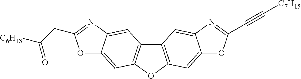 |
B | B | B | B | A |
| Compound 46 |
 |
C | B | B | B | B |
| Compound 47 |
 |
A | B | A | A | A |
| Compound 48 |
 |
A | A | A | B | A |
| Compound 49 |
 |
B | B | B | | B |
| Compound | ||||||
| 50 |
 |
B | B | B | | A |
| Compound | ||||||
| 51 |
 |
C | B | B | A | A |
| Compound 52 |
 |
C | B | B | A | A |
| Compound 53 |
 |
C | B | B | B | B |
| Compound 54 |
 |
B | B | B | A | A |
| Compound 55 |
 |
C | B | B | A | A |
| TABLE 66 | ||||||
| Average | Variation in | Vth | ||||
| Mobility | Mobility | Yield | Shift | Hysteresis | ||
| Compound 56 |
 |
B | B | B | B | B |
| Compound 57 |
 |
C | C | B | C | B |
| Compound 58 |
 |
B | B | B | B | B |
| Compound 59 |
 |
B | B | B | | A |
| Compound | ||||||
| 60 |
 |
B | B | B | | A |
| Compound | ||||||
| 61 |
 |
C | B | B | A | A |
| Compound 62 |
 |
A | A | A | A | A |
| Compound 63 |
 |
A | A | A | B | A |
| Compound 64 |
 |
A | B | A | B | B |
| Compound 65 |
 |
C | C | B | C | C |
| Compound 66 |
 |
C | B | B | B | B |
| TABLE 67 | ||||||
| Average | Variation in | Vth | ||||
| Mobility | Mobility | Yield | Shift | Hysteresis | ||
| Compound 67 |
 |
B | B | B | B | B |
| Compound 68 |
 |
A | B | A | A | A |
| Compound 69 |
 |
B | B | B | A | A |
| Compound 70 |
 |
B | B | B | A | A |
| Compound 71 |
 |
A | B | B | A | A |
| Compound 72 |
 |
B | B | C | B | B |
| Compound 73 |
 |
B | B | C | B | B |
| Compound 74 |
 |
C | B | C | B | B |
| Compound 75 |
 |
C | C | C | C | C |
| Compound 76 |
 |
C | C | C | C | C |
| Compound 77 |
 |
C | C | C | C | C |
| TABLE 68 | ||||||
| Average | Variation in | Vth | ||||
| Mobility | Mobility | Yield | Shift | Hysteresis | ||
| Compound 78 |
 |
B | B | A | A | A |
| Compound 79 |
 |
C | B | B | A | A |
| Compound 80 |
 |
B | C | C | B | A |
| Compound 81 |
 |
B | B | B | A | A |
| Compound 82 |
 |
B | B | B | A | A |
| Compound 83 |
 |
B | B | B | B | A |
| Compound 84 |
 |
C | B | B | A | A |
| Compound 85 |
 |
C | C | C | C | C |
| Compound 86 |
 |
C | B | B | A | B |
| Compound 87 |
 |
C | C | C | C | C |
| Compound 88 |
 |
B | B | B | B | B |
| TABLE 69 | ||||||
| Variation | ||||||
| Average | in | Vth | Hys- | |||
| Mobility | Mobility | Yield | Shift | teresis | ||
| Compound 89 |
 |
C | C | B | B | B |
| Compound 90 |
 |
B | B | B | A | A |
| Compound 91 |
 |
B | B | B | A | A |
| Compound 92 |
 |
B | B | B | A | A |
| Compound 93 |
 |
C | B | B | B | A |
| Compound 94 |
 |
C | C | C | B | B |
| Compound 95 |
 |
B | B | B | B | B |
| Compound 96 |
 |
B | B | B | B | B |
| Compound 97 |
 |
B | B | B | C | B |
| Compound 98 |
 |
B | B | B | B | B |
| Compound 99 |
 |
B | B | B | C | B |
| TABLE 70 | ||||||
| Variation | ||||||
| Average | in | Vth | Hys- | |||
| Mobility | Mobility | Yield | | teresis | ||
| Compound | ||||||
| 100 |
 |
C | C | C | B | B |
| Compound 101 |
 |
C | C | C | B | B |
| Compound 102 |
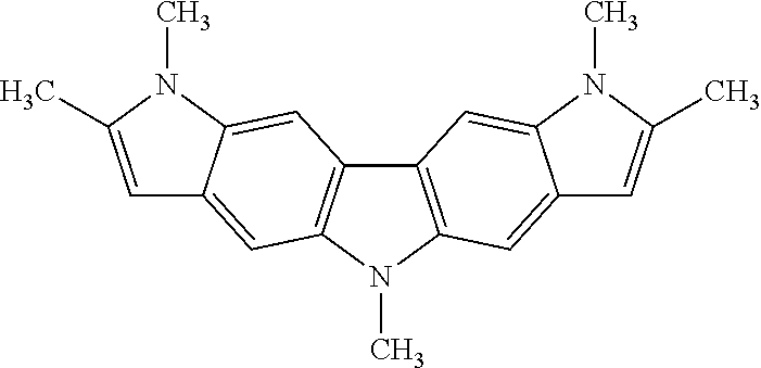 |
B | B | B | B | B |
| Compound 103 |
 |
B | A | A | A | A |
| Compound 104 |
 |
B | A | A | A | A |
| Compound 105 |
 |
A | B | A | B | A |
| Compound 106 |
 |
A | B | A | B | A |
| Compound 107 |
 |
A | A | A | B | A |
| Compound 108 |
 |
A | B | A | B | A |
| |
 |
D | C | D | B | |
| Comparative Compound | ||||||
| 2 |
 |
E | D | E | B | |
| Comparative Compound | ||||||
| 3 |
 |
E | C | E | B | |
| Comparative Compound | ||||||
| 4 |
 |
E | C | E | B | B |
| TABLE 71 | |||||||
| Average | Variation in | Vth | |||||
| Compound | Mobility | Mobility | Yield | Shift | Hysteresis | ||
| Manufacturing Example 1-1 | Compound | A | A | | A | A | |
| 1 | |||||||
| Comparative | Compound | A | C | D | D | B | |
| Manufacturing Example 1-5 | 1 | ||||||
| TABLE 72 | |||||||
| Average | Variation in | Vth | |||||
| Compound | Mobility | Mobility | Yield | Shift | Hysteresis | ||
| Manufacturing Example 2-1 | Compound | A | A | | A | A | |
| 1 | |||||||
| Comparative | Compound | B | E | E | D | B | |
| Manufacturing Example 2-5 | 1 | ||||||
| TABLE 73 | |||||||
| Average | Variation in | Vth | |||||
| Compound | Mobility | Mobility | Yield | Shift | Hysteresis | ||
| Manufacturing Example 3-1 | Compound | A | A | | A | A | |
| 1 | |||||||
| Comparative | Compound | C | D | D | B | B | |
| Manufacturing Example 3-5 | 1 | ||||||
| TABLE 74 | ||||||
| Average | Variation in | Vth | ||||
| Compound | Mobility | Mobility | Yield | Shift | Hysteresis | |
| Manufacturing Example | Compound 1 | A | A | A | A | A |
| 4-1 | ||||||
| Comparative | Compound 1 | C | E | E | C | C |
| Manufacturing Example | ||||||
| 4-5 | ||||||
-
- 10: substrate
- 20: gate electrode
- 30: gate insulating layer (film)
- 40: source electrode
- 42: drain electrode
- 50: organic semiconductor layer (film)
- 60: sealing layer
- 100, 200: organic semiconductor transistor
- 21: silicon substrate (gate electrode)
- 31: thermal oxide film (gate insulating layer)
- 41 a: source electrode
- 41 b: drain electrode
- 51: organic semiconductor layer
- 61: sealing layer
- 300, 400: organic semiconductor transistor
Claims (21)


Applications Claiming Priority (4)
| Application Number | Priority Date | Filing Date | Title |
|---|---|---|---|
| JP2016191913 | 2016-09-29 | ||
| JP2016-191913 | 2016-09-29 | ||
| JPJP2016-191913 | 2016-09-29 | ||
| PCT/JP2017/033407 WO2018061819A1 (en) | 2016-09-29 | 2017-09-15 | Microcrystalline organic semiconductor film, organic semiconductor transistor, and method for producing organic semiconductor transistor |
Related Parent Applications (1)
| Application Number | Title | Priority Date | Filing Date |
|---|---|---|---|
| PCT/JP2017/033407 Continuation WO2018061819A1 (en) | 2016-09-29 | 2017-09-15 | Microcrystalline organic semiconductor film, organic semiconductor transistor, and method for producing organic semiconductor transistor |
Publications (2)
| Publication Number | Publication Date |
|---|---|
| US20190237677A1 US20190237677A1 (en) | 2019-08-01 |
| US10985327B2 true US10985327B2 (en) | 2021-04-20 |
Family
ID=61760297
Family Applications (1)
| Application Number | Title | Priority Date | Filing Date |
|---|---|---|---|
| US16/358,910 Active 2037-11-08 US10985327B2 (en) | 2016-09-29 | 2019-03-20 | Microcrystalline organic semiconductor film, organic semiconductor transistor, and method of manufacturing organic semiconductor transistor |
Country Status (6)
| Country | Link |
|---|---|
| US (1) | US10985327B2 (en) |
| EP (1) | EP3522244B1 (en) |
| JP (1) | JP6676181B2 (en) |
| CN (1) | CN109791983B (en) |
| TW (1) | TWI724241B (en) |
| WO (1) | WO2018061819A1 (en) |
Families Citing this family (4)
| Publication number | Priority date | Publication date | Assignee | Title |
|---|---|---|---|---|
| CN108933179B (en) * | 2018-07-05 | 2020-06-16 | 深圳市华星光电半导体显示技术有限公司 | Thin film transistor and manufacturing method thereof |
| JP7494456B2 (en) * | 2018-09-28 | 2024-06-04 | 東ソー株式会社 | Biphenylene derivative, organic semiconductor layer, and organic thin film transistor |
| CN113355105A (en) * | 2020-03-06 | 2021-09-07 | 石家庄诚志永华显示材料有限公司 | Liquid crystal compound containing dibenzothiophene and oxygen-containing heterocycle and application thereof |
| CN114560875B (en) * | 2022-02-14 | 2023-04-18 | 西安凯翔光电科技有限公司 | Organic covering layer material and organic electroluminescent device |
Citations (7)
| Publication number | Priority date | Publication date | Assignee | Title |
|---|---|---|---|---|
| JP2008085250A (en) | 2006-09-29 | 2008-04-10 | Sony Corp | Semiconductor device |
| WO2011126225A1 (en) * | 2010-04-09 | 2011-10-13 | Rohm And Haas Electronic Materials Korea Ltd. | Novel compounds for organic electronic material and organic electroluminescent device using the same |
| WO2015128779A1 (en) | 2014-02-25 | 2015-09-03 | Basf Se | Heteroacenes for organic electronics |
| JP2015195362A (en) | 2014-03-26 | 2015-11-05 | 富士フイルム株式会社 | Organic transistor, compound, organic semiconductor material for nonluminous organic semiconductor devices, material for organic transistors, coating liquid for nonluminous organic semiconductor devices, method for manufacturing organic transistor, method for manufacturing organic semiconductor film, organic semiconductor film for nonluminous organic semiconductor devices, and method for synthesizing organic semiconductor material |
| JP2015195361A (en) | 2014-03-26 | 2015-11-05 | 富士フイルム株式会社 | Provision of coating liquid for nonluminous organic semiconductor devices, organic transistor, compound, organic semiconductor material for nonluminous organic semiconductor devices, material for organic transistors, method for manufacturing organic transistor, and method for manufacturing organic semiconductor film |
| US20150340630A1 (en) | 2014-05-23 | 2015-11-26 | Industry-Academic Cooperation Foundation, Yonsei University | Flexible organic thin-film transistor and sensor having the same |
| WO2016047587A1 (en) | 2014-09-25 | 2016-03-31 | 富士フイルム株式会社 | Organic field effect transistor, method for producing organic semiconductor crystal, and organic semiconductor element |
Family Cites Families (14)
| Publication number | Priority date | Publication date | Assignee | Title |
|---|---|---|---|---|
| JP4731840B2 (en) | 2004-06-14 | 2011-07-27 | キヤノン株式会社 | Field effect transistor and manufacturing method thereof |
| JP5037841B2 (en) | 2005-03-25 | 2012-10-03 | キヤノン株式会社 | ORGANIC SEMICONDUCTOR DEVICE, FIELD EFFECT TRANSISTOR AND METHOD FOR PRODUCING THEM |
| TWI471328B (en) * | 2008-07-02 | 2015-02-01 | 巴地斯顏料化工廠 | High-performance solution processable semiconductor mainly composed of dithieno[2,3-d:2',3'-d']benzo[1,2-b:4,5-b']dithiophene |
| KR101805203B1 (en) * | 2009-05-27 | 2018-01-10 | 바스프 에스이 | Polycyclic dithiophenes |
| JP5284880B2 (en) | 2009-06-10 | 2013-09-11 | 株式会社カネカ | Photocurable composition and insulating thin film and thin film transistor using the same |
| JP2011186069A (en) | 2010-03-05 | 2011-09-22 | Adeka Corp | Photosensitive resin composition |
| JP5703197B2 (en) | 2011-01-18 | 2015-04-15 | 富士フイルム株式会社 | Chemically amplified resist composition, resist film using the same, resist coating mask blank, resist pattern forming method, photomask, and polymer compound |
| JP2013214649A (en) | 2012-04-03 | 2013-10-17 | Asahi Glass Co Ltd | Semiconductor device and method for manufacturing the same |
| JP6174404B2 (en) * | 2013-07-19 | 2017-08-02 | 富士フイルム株式会社 | Organic thin film transistor, organic semiconductor thin film and organic semiconductor material |
| JP6247560B2 (en) * | 2014-02-20 | 2017-12-13 | 富士フイルム株式会社 | Organic thin film transistor, organic semiconductor thin film and organic semiconductor material |
| JP6247568B2 (en) * | 2014-03-03 | 2017-12-13 | 富士フイルム株式会社 | Organic thin-film transistors, organic semiconductor materials for non-emissive organic semiconductor devices and their applications |
| WO2016071140A1 (en) * | 2014-11-04 | 2016-05-12 | Basf Se | Phenacene compounds for organic electronics |
| JP6274529B2 (en) * | 2015-02-09 | 2018-02-07 | 富士フイルム株式会社 | ORGANIC SEMICONDUCTOR DEVICE AND ITS MANUFACTURING METHOD, ORGANIC SEMICONDUCTOR FILM FORMING COMPOSITION, AND ORGANIC SEMICONDUCTOR FILM MANUFACTURING METHOD |
| US9766446B2 (en) | 2015-03-30 | 2017-09-19 | Keysight Technologies, Inc. | Microscope illumination system |
-
2017
- 2017-09-15 WO PCT/JP2017/033407 patent/WO2018061819A1/en not_active Ceased
- 2017-09-15 CN CN201780057197.4A patent/CN109791983B/en active Active
- 2017-09-15 EP EP17855775.7A patent/EP3522244B1/en active Active
- 2017-09-15 JP JP2018542392A patent/JP6676181B2/en active Active
- 2017-09-26 TW TW106132991A patent/TWI724241B/en active
-
2019
- 2019-03-20 US US16/358,910 patent/US10985327B2/en active Active
Patent Citations (11)
| Publication number | Priority date | Publication date | Assignee | Title |
|---|---|---|---|---|
| JP2008085250A (en) | 2006-09-29 | 2008-04-10 | Sony Corp | Semiconductor device |
| WO2011126225A1 (en) * | 2010-04-09 | 2011-10-13 | Rohm And Haas Electronic Materials Korea Ltd. | Novel compounds for organic electronic material and organic electroluminescent device using the same |
| WO2015128779A1 (en) | 2014-02-25 | 2015-09-03 | Basf Se | Heteroacenes for organic electronics |
| US20160365519A1 (en) | 2014-02-25 | 2016-12-15 | Basf Se | Heteroacenes for organic electronics |
| JP2015195362A (en) | 2014-03-26 | 2015-11-05 | 富士フイルム株式会社 | Organic transistor, compound, organic semiconductor material for nonluminous organic semiconductor devices, material for organic transistors, coating liquid for nonluminous organic semiconductor devices, method for manufacturing organic transistor, method for manufacturing organic semiconductor film, organic semiconductor film for nonluminous organic semiconductor devices, and method for synthesizing organic semiconductor material |
| JP2015195361A (en) | 2014-03-26 | 2015-11-05 | 富士フイルム株式会社 | Provision of coating liquid for nonluminous organic semiconductor devices, organic transistor, compound, organic semiconductor material for nonluminous organic semiconductor devices, material for organic transistors, method for manufacturing organic transistor, and method for manufacturing organic semiconductor film |
| US20170012220A1 (en) | 2014-03-26 | 2017-01-12 | Fujifilm Corporation | Coating solution for non-light-emitting organic semiconductor device, organic transistor, compound, organic semiconductor material for non-light-emitting organic semiconductor device, material for organic transistor, method for manufacturing organic transistor, and method for manufacturing organic semiconductor film |
| US20170018724A1 (en) | 2014-03-26 | 2017-01-19 | Fujifilm Corporation | Organic transistor, compound, organic semiconductor material for non-light-emitting organic semiconductor device, material for organic transistor, coating solution for non-light-emitting organic semiconductor device, method for manufacturing organic transistor, method for manufacturing organic semiconductor film, organic semiconductor film for non-light-emitting organic semiconductor device, and method for synthesizing organic semiconductor material |
| US20150340630A1 (en) | 2014-05-23 | 2015-11-26 | Industry-Academic Cooperation Foundation, Yonsei University | Flexible organic thin-film transistor and sensor having the same |
| WO2016047587A1 (en) | 2014-09-25 | 2016-03-31 | 富士フイルム株式会社 | Organic field effect transistor, method for producing organic semiconductor crystal, and organic semiconductor element |
| US20170179415A1 (en) | 2014-09-25 | 2017-06-22 | Fujifilm Corporation | Organic field-effect transistor, method for manufacturing organic semiconductor crystal, and organic semiconductor element |
Non-Patent Citations (4)
| Title |
|---|
| An Office Action mailed by the Japanese Patent Office dated Nov. 26, 2019, which corresponds to Japanese Patent Application No. 2018-542392 and is related to U.S. Appl. No. 16/358,910. |
| Extended European Search Report issued by the European Patent Office dated Oct. 9, 2019, which corresponds to EP17855775.7-1211 and is related to U.S. Appl. No. 16/358,910. |
| International Search Report issued in PCT/JP2017/033407; dated Nov. 7, 2017. |
| Written Opinion of the International Searching Authority issued in PCT/JP2017/033407; dated Nov. 7, 2017. |
Also Published As
| Publication number | Publication date |
|---|---|
| CN109791983B (en) | 2023-06-16 |
| EP3522244A1 (en) | 2019-08-07 |
| WO2018061819A1 (en) | 2018-04-05 |
| EP3522244A4 (en) | 2019-11-06 |
| JPWO2018061819A1 (en) | 2019-03-22 |
| US20190237677A1 (en) | 2019-08-01 |
| EP3522244B1 (en) | 2020-07-15 |
| TWI724241B (en) | 2021-04-11 |
| CN109791983A (en) | 2019-05-21 |
| TW201819390A (en) | 2018-06-01 |
| JP6676181B2 (en) | 2020-04-08 |
Similar Documents
| Publication | Publication Date | Title |
|---|---|---|
| US10985327B2 (en) | Microcrystalline organic semiconductor film, organic semiconductor transistor, and method of manufacturing organic semiconductor transistor | |
| KR20160127074A (en) | Coating solution for non-emissive organic semiconductor device, organic transistor, compound, organic semiconductor material for non-emissive organic semiconductor device, material for organic transistor, method for manufacturing organic transistor, and method for manufacturing organic semiconductor film | |
| JP6689393B2 (en) | Composition for forming organic semiconductor film, organic semiconductor film and method for producing the same, and organic semiconductor element | |
| US9203038B2 (en) | Electronic device | |
| US8643001B2 (en) | Semiconductor composition | |
| US9680112B2 (en) | Semiconductor composition | |
| US8994016B2 (en) | Dielectric layer for an electronic device | |
| US20180175300A1 (en) | Organic thin film transistor, method of manufacturing organic thin film transistor, organic semiconductor composition, organic semiconductor film, and method of manufacturing organic semiconductor film | |
| US10651400B2 (en) | Organic semiconductor element, manufacturing method thereof, composition for forming organic semiconductor film, and method of manufacturing organic semiconductor film | |
| CN108780844B (en) | Organic semiconductor composition, method for producing organic thin film transistor, and organic thin film transistor | |
| US11133475B2 (en) | Organic semiconductor element, organic semiconductor composition, method of manufacturing organic semiconductor film, organic semiconductor film, and compound and polymer using the same | |
| US20190221754A1 (en) | Bottom gate type organic semiconductor transistor | |
| US11081651B2 (en) | Organic semiconductor element, organic semiconductor composition, method of manufacturing organic semiconductor film, organic semiconductor film, and compound and polymer using the same | |
| US9954183B2 (en) | Intermediate for heteroacene compound and synthetic method of heteroacene compound using its intermediate | |
| JP7316365B2 (en) | Compounds, compositions, films, structures and electronic devices | |
| US7573063B1 (en) | Organic thin film transistors | |
| US20200028096A1 (en) | Organic semiconductor element, organic semiconductor composition, method of manufacturing organic semiconductor film, organic semiconductor film, and compound and polymer using the same | |
| US10553798B2 (en) | Fused polycyclic heteroaromatic compound, organic thin film including compound and electronic device including organic thin film | |
| US8420440B2 (en) | Semiconducting composition | |
| US11038125B2 (en) | Organic semiconductor element, polymer, organic semiconductor composition, and organic semiconductor film | |
| US20180175299A1 (en) | Organic thin film transistor, method of manufacturing organic thin film transistor, organic semiconductor composition, organic semiconductor film, and method of manufacturing organic semiconductor film |
Legal Events
| Date | Code | Title | Description |
|---|---|---|---|
| AS | Assignment |
Owner name: FUJIFILM CORPORATION, JAPAN Free format text: ASSIGNMENT OF ASSIGNORS INTEREST;ASSIGNORS:GOTO, TAKASHI;FUKUZAKI, EIJI;WATANABE, TETSUYA;SIGNING DATES FROM 20190109 TO 20190124;REEL/FRAME:048645/0355 |
|
| FEPP | Fee payment procedure |
Free format text: ENTITY STATUS SET TO UNDISCOUNTED (ORIGINAL EVENT CODE: BIG.); ENTITY STATUS OF PATENT OWNER: LARGE ENTITY |
|
| STPP | Information on status: patent application and granting procedure in general |
Free format text: DOCKETED NEW CASE - READY FOR EXAMINATION |
|
| STPP | Information on status: patent application and granting procedure in general |
Free format text: NOTICE OF ALLOWANCE MAILED -- APPLICATION RECEIVED IN OFFICE OF PUBLICATIONS |
|
| STPP | Information on status: patent application and granting procedure in general |
Free format text: PUBLICATIONS -- ISSUE FEE PAYMENT VERIFIED |
|
| STCF | Information on status: patent grant |
Free format text: PATENTED CASE |
|
| MAFP | Maintenance fee payment |
Free format text: PAYMENT OF MAINTENANCE FEE, 4TH YEAR, LARGE ENTITY (ORIGINAL EVENT CODE: M1551); ENTITY STATUS OF PATENT OWNER: LARGE ENTITY Year of fee payment: 4 |