US10984994B2 - Deposition apparatus and physical vapor deposition chamber - Google Patents
Deposition apparatus and physical vapor deposition chamber Download PDFInfo
- Publication number
- US10984994B2 US10984994B2 US15/551,493 US201615551493A US10984994B2 US 10984994 B2 US10984994 B2 US 10984994B2 US 201615551493 A US201615551493 A US 201615551493A US 10984994 B2 US10984994 B2 US 10984994B2
- Authority
- US
- United States
- Prior art keywords
- chamber
- substrate
- pvd
- shielding plate
- target
- Prior art date
- Legal status (The legal status is an assumption and is not a legal conclusion. Google has not performed a legal analysis and makes no representation as to the accuracy of the status listed.)
- Active, expires
Links
- 238000000151 deposition Methods 0.000 title claims abstract description 47
- 230000008021 deposition Effects 0.000 title claims abstract description 47
- 238000005240 physical vapour deposition Methods 0.000 title claims description 93
- 239000000758 substrate Substances 0.000 claims abstract description 120
- 238000000034 method Methods 0.000 claims abstract description 113
- 230000008569 process Effects 0.000 claims abstract description 113
- 238000004544 sputter deposition Methods 0.000 claims abstract description 43
- 230000000694 effects Effects 0.000 claims description 19
- 238000010438 heat treatment Methods 0.000 claims description 14
- 239000002245 particle Substances 0.000 claims description 10
- 230000004048 modification Effects 0.000 claims description 9
- 238000012986 modification Methods 0.000 claims description 9
- 230000003213 activating effect Effects 0.000 claims description 7
- PMHQVHHXPFUNSP-UHFFFAOYSA-M copper(1+);methylsulfanylmethane;bromide Chemical compound Br[Cu].CSC PMHQVHHXPFUNSP-UHFFFAOYSA-M 0.000 claims description 7
- 238000007872 degassing Methods 0.000 claims description 7
- 239000000853 adhesive Substances 0.000 claims description 6
- 230000001070 adhesive effect Effects 0.000 claims description 6
- 238000001816 cooling Methods 0.000 claims description 4
- 238000010586 diagram Methods 0.000 description 20
- 239000000463 material Substances 0.000 description 13
- 238000004519 manufacturing process Methods 0.000 description 8
- 230000009471 action Effects 0.000 description 6
- 230000007547 defect Effects 0.000 description 5
- 238000004904 shortening Methods 0.000 description 5
- 238000002425 crystallisation Methods 0.000 description 3
- 230000008025 crystallization Effects 0.000 description 3
- 229910052751 metal Inorganic materials 0.000 description 3
- 239000002184 metal Substances 0.000 description 3
- 230000008092 positive effect Effects 0.000 description 3
- ZOKXTWBITQBERF-UHFFFAOYSA-N Molybdenum Chemical compound [Mo] ZOKXTWBITQBERF-UHFFFAOYSA-N 0.000 description 2
- XUIMIQQOPSSXEZ-UHFFFAOYSA-N Silicon Chemical compound [Si] XUIMIQQOPSSXEZ-UHFFFAOYSA-N 0.000 description 2
- 230000008901 benefit Effects 0.000 description 2
- 229910052750 molybdenum Inorganic materials 0.000 description 2
- 239000011733 molybdenum Substances 0.000 description 2
- 230000001737 promoting effect Effects 0.000 description 2
- 239000004065 semiconductor Substances 0.000 description 2
- 229910052710 silicon Inorganic materials 0.000 description 2
- 239000010703 silicon Substances 0.000 description 2
- HBMJWWWQQXIZIP-UHFFFAOYSA-N silicon carbide Chemical compound [Si+]#[C-] HBMJWWWQQXIZIP-UHFFFAOYSA-N 0.000 description 2
- 238000005477 sputtering target Methods 0.000 description 2
- 230000000087 stabilizing effect Effects 0.000 description 2
- 238000003466 welding Methods 0.000 description 2
- PIGFYZPCRLYGLF-UHFFFAOYSA-N Aluminum nitride Chemical compound [Al]#N PIGFYZPCRLYGLF-UHFFFAOYSA-N 0.000 description 1
- OKTJSMMVPCPJKN-UHFFFAOYSA-N Carbon Chemical compound [C] OKTJSMMVPCPJKN-UHFFFAOYSA-N 0.000 description 1
- 229910052799 carbon Inorganic materials 0.000 description 1
- 239000000919 ceramic Substances 0.000 description 1
- 230000008859 change Effects 0.000 description 1
- 238000006243 chemical reaction Methods 0.000 description 1
- 238000004140 cleaning Methods 0.000 description 1
- 239000002131 composite material Substances 0.000 description 1
- 238000006073 displacement reaction Methods 0.000 description 1
- 230000002708 enhancing effect Effects 0.000 description 1
- 239000011521 glass Substances 0.000 description 1
- 230000005484 gravity Effects 0.000 description 1
- 239000012212 insulator Substances 0.000 description 1
- 150000002500 ions Chemical class 0.000 description 1
- 238000002844 melting Methods 0.000 description 1
- 230000008018 melting Effects 0.000 description 1
- 150000002736 metal compounds Chemical class 0.000 description 1
- 230000002093 peripheral effect Effects 0.000 description 1
- 239000010453 quartz Substances 0.000 description 1
- 230000000630 rising effect Effects 0.000 description 1
- 238000007788 roughening Methods 0.000 description 1
- 238000005488 sandblasting Methods 0.000 description 1
- 229910052594 sapphire Inorganic materials 0.000 description 1
- 239000010980 sapphire Substances 0.000 description 1
- 238000007789 sealing Methods 0.000 description 1
- VYPSYNLAJGMNEJ-UHFFFAOYSA-N silicon dioxide Inorganic materials O=[Si]=O VYPSYNLAJGMNEJ-UHFFFAOYSA-N 0.000 description 1
- 229910001220 stainless steel Inorganic materials 0.000 description 1
- 239000010935 stainless steel Substances 0.000 description 1
- 230000008093 supporting effect Effects 0.000 description 1
- 238000004381 surface treatment Methods 0.000 description 1
- 239000013077 target material Substances 0.000 description 1
Images


Classifications
-
- H—ELECTRICITY
- H01—ELECTRIC ELEMENTS
- H01J—ELECTRIC DISCHARGE TUBES OR DISCHARGE LAMPS
- H01J37/00—Discharge tubes with provision for introducing objects or material to be exposed to the discharge, e.g. for the purpose of examination or processing thereof
- H01J37/32—Gas-filled discharge tubes
- H01J37/34—Gas-filled discharge tubes operating with cathodic sputtering
- H01J37/3488—Constructional details of particle beam apparatus not otherwise provided for, e.g. arrangement, mounting, housing, environment; special provisions for cleaning or maintenance of the apparatus
-
- C—CHEMISTRY; METALLURGY
- C23—COATING METALLIC MATERIAL; COATING MATERIAL WITH METALLIC MATERIAL; CHEMICAL SURFACE TREATMENT; DIFFUSION TREATMENT OF METALLIC MATERIAL; COATING BY VACUUM EVAPORATION, BY SPUTTERING, BY ION IMPLANTATION OR BY CHEMICAL VAPOUR DEPOSITION, IN GENERAL; INHIBITING CORROSION OF METALLIC MATERIAL OR INCRUSTATION IN GENERAL
- C23C—COATING METALLIC MATERIAL; COATING MATERIAL WITH METALLIC MATERIAL; SURFACE TREATMENT OF METALLIC MATERIAL BY DIFFUSION INTO THE SURFACE, BY CHEMICAL CONVERSION OR SUBSTITUTION; COATING BY VACUUM EVAPORATION, BY SPUTTERING, BY ION IMPLANTATION OR BY CHEMICAL VAPOUR DEPOSITION, IN GENERAL
- C23C14/00—Coating by vacuum evaporation, by sputtering or by ion implantation of the coating forming material
- C23C14/06—Coating by vacuum evaporation, by sputtering or by ion implantation of the coating forming material characterised by the coating material
- C23C14/0641—Nitrides
-
- C—CHEMISTRY; METALLURGY
- C23—COATING METALLIC MATERIAL; COATING MATERIAL WITH METALLIC MATERIAL; CHEMICAL SURFACE TREATMENT; DIFFUSION TREATMENT OF METALLIC MATERIAL; COATING BY VACUUM EVAPORATION, BY SPUTTERING, BY ION IMPLANTATION OR BY CHEMICAL VAPOUR DEPOSITION, IN GENERAL; INHIBITING CORROSION OF METALLIC MATERIAL OR INCRUSTATION IN GENERAL
- C23C—COATING METALLIC MATERIAL; COATING MATERIAL WITH METALLIC MATERIAL; SURFACE TREATMENT OF METALLIC MATERIAL BY DIFFUSION INTO THE SURFACE, BY CHEMICAL CONVERSION OR SUBSTITUTION; COATING BY VACUUM EVAPORATION, BY SPUTTERING, BY ION IMPLANTATION OR BY CHEMICAL VAPOUR DEPOSITION, IN GENERAL
- C23C14/00—Coating by vacuum evaporation, by sputtering or by ion implantation of the coating forming material
- C23C14/22—Coating by vacuum evaporation, by sputtering or by ion implantation of the coating forming material characterised by the process of coating
- C23C14/34—Sputtering
-
- C—CHEMISTRY; METALLURGY
- C23—COATING METALLIC MATERIAL; COATING MATERIAL WITH METALLIC MATERIAL; CHEMICAL SURFACE TREATMENT; DIFFUSION TREATMENT OF METALLIC MATERIAL; COATING BY VACUUM EVAPORATION, BY SPUTTERING, BY ION IMPLANTATION OR BY CHEMICAL VAPOUR DEPOSITION, IN GENERAL; INHIBITING CORROSION OF METALLIC MATERIAL OR INCRUSTATION IN GENERAL
- C23C—COATING METALLIC MATERIAL; COATING MATERIAL WITH METALLIC MATERIAL; SURFACE TREATMENT OF METALLIC MATERIAL BY DIFFUSION INTO THE SURFACE, BY CHEMICAL CONVERSION OR SUBSTITUTION; COATING BY VACUUM EVAPORATION, BY SPUTTERING, BY ION IMPLANTATION OR BY CHEMICAL VAPOUR DEPOSITION, IN GENERAL
- C23C14/00—Coating by vacuum evaporation, by sputtering or by ion implantation of the coating forming material
- C23C14/22—Coating by vacuum evaporation, by sputtering or by ion implantation of the coating forming material characterised by the process of coating
- C23C14/50—Substrate holders
-
- C—CHEMISTRY; METALLURGY
- C23—COATING METALLIC MATERIAL; COATING MATERIAL WITH METALLIC MATERIAL; CHEMICAL SURFACE TREATMENT; DIFFUSION TREATMENT OF METALLIC MATERIAL; COATING BY VACUUM EVAPORATION, BY SPUTTERING, BY ION IMPLANTATION OR BY CHEMICAL VAPOUR DEPOSITION, IN GENERAL; INHIBITING CORROSION OF METALLIC MATERIAL OR INCRUSTATION IN GENERAL
- C23C—COATING METALLIC MATERIAL; COATING MATERIAL WITH METALLIC MATERIAL; SURFACE TREATMENT OF METALLIC MATERIAL BY DIFFUSION INTO THE SURFACE, BY CHEMICAL CONVERSION OR SUBSTITUTION; COATING BY VACUUM EVAPORATION, BY SPUTTERING, BY ION IMPLANTATION OR BY CHEMICAL VAPOUR DEPOSITION, IN GENERAL
- C23C14/00—Coating by vacuum evaporation, by sputtering or by ion implantation of the coating forming material
- C23C14/22—Coating by vacuum evaporation, by sputtering or by ion implantation of the coating forming material characterised by the process of coating
- C23C14/56—Apparatus specially adapted for continuous coating; Arrangements for maintaining the vacuum, e.g. vacuum locks
- C23C14/564—Means for minimising impurities in the coating chamber such as dust, moisture, residual gases
- C23C14/566—Means for minimising impurities in the coating chamber such as dust, moisture, residual gases using a load-lock chamber
-
- C—CHEMISTRY; METALLURGY
- C23—COATING METALLIC MATERIAL; COATING MATERIAL WITH METALLIC MATERIAL; CHEMICAL SURFACE TREATMENT; DIFFUSION TREATMENT OF METALLIC MATERIAL; COATING BY VACUUM EVAPORATION, BY SPUTTERING, BY ION IMPLANTATION OR BY CHEMICAL VAPOUR DEPOSITION, IN GENERAL; INHIBITING CORROSION OF METALLIC MATERIAL OR INCRUSTATION IN GENERAL
- C23C—COATING METALLIC MATERIAL; COATING MATERIAL WITH METALLIC MATERIAL; SURFACE TREATMENT OF METALLIC MATERIAL BY DIFFUSION INTO THE SURFACE, BY CHEMICAL CONVERSION OR SUBSTITUTION; COATING BY VACUUM EVAPORATION, BY SPUTTERING, BY ION IMPLANTATION OR BY CHEMICAL VAPOUR DEPOSITION, IN GENERAL
- C23C14/00—Coating by vacuum evaporation, by sputtering or by ion implantation of the coating forming material
- C23C14/22—Coating by vacuum evaporation, by sputtering or by ion implantation of the coating forming material characterised by the process of coating
- C23C14/56—Apparatus specially adapted for continuous coating; Arrangements for maintaining the vacuum, e.g. vacuum locks
- C23C14/568—Transferring the substrates through a series of coating stations
-
- H—ELECTRICITY
- H01—ELECTRIC ELEMENTS
- H01J—ELECTRIC DISCHARGE TUBES OR DISCHARGE LAMPS
- H01J37/00—Discharge tubes with provision for introducing objects or material to be exposed to the discharge, e.g. for the purpose of examination or processing thereof
- H01J37/32—Gas-filled discharge tubes
- H01J37/32431—Constructional details of the reactor
- H01J37/32532—Electrodes
- H01J37/32559—Protection means, e.g. coatings
-
- H—ELECTRICITY
- H01—ELECTRIC ELEMENTS
- H01J—ELECTRIC DISCHARGE TUBES OR DISCHARGE LAMPS
- H01J37/00—Discharge tubes with provision for introducing objects or material to be exposed to the discharge, e.g. for the purpose of examination or processing thereof
- H01J37/32—Gas-filled discharge tubes
- H01J37/32431—Constructional details of the reactor
- H01J37/32733—Means for moving the material to be treated
-
- H—ELECTRICITY
- H01—ELECTRIC ELEMENTS
- H01J—ELECTRIC DISCHARGE TUBES OR DISCHARGE LAMPS
- H01J37/00—Discharge tubes with provision for introducing objects or material to be exposed to the discharge, e.g. for the purpose of examination or processing thereof
- H01J37/32—Gas-filled discharge tubes
- H01J37/32431—Constructional details of the reactor
- H01J37/32798—Further details of plasma apparatus not provided for in groups H01J37/3244 - H01J37/32788; special provisions for cleaning or maintenance of the apparatus
- H01J37/32899—Multiple chambers, e.g. cluster tools
-
- H—ELECTRICITY
- H01—ELECTRIC ELEMENTS
- H01J—ELECTRIC DISCHARGE TUBES OR DISCHARGE LAMPS
- H01J37/00—Discharge tubes with provision for introducing objects or material to be exposed to the discharge, e.g. for the purpose of examination or processing thereof
- H01J37/32—Gas-filled discharge tubes
- H01J37/34—Gas-filled discharge tubes operating with cathodic sputtering
- H01J37/3411—Constructional aspects of the reactor
- H01J37/3414—Targets
- H01J37/3426—Material
Definitions
- the present disclosure relates to a semiconductor process apparatus, and particularly relates to a deposition apparatus and a physical vapor deposition chamber.
- PVD Physical vapor deposition
- LEDs light emitting diodes
- a process chamber of a PVD apparatus working gas in a reaction chamber is excited into plasma by a high-power direct-current power supply connected to a sputtering target, and ions in the plasma are attracted to bombard the sputtering target, so that the material of the target is sputtered off and deposited on a wafer or other substrate.
- Different application areas usually have different requirements for sputtering power, sputtering rate and other process parameters, but substantially have a clear striving direction of improving film-formation quality and increasing apparatus capacity.
- the present disclosure provides a deposition apparatus and a PVD chamber, wherein a heat source that can heat the chamber to 400 degrees Celsius or more is provided in the PVD chamber, thus, the loaded substrate can be preheated, degassed and sputtered in the high temperature environment of the PVD chamber, and as a result, effects of reducing apparatus volume and cost, shortening process time, promoting production capacity and the like can be achieved.
- Some embodiments of the present disclosure provide a deposition apparatus, which includes a first chamber, a second chamber and a third chamber.
- the first chamber is configured to load a substrate.
- the second chamber is configured to provide a high temperature environment so that a degas process and a sputtering process are performed on the substrate in the second chamber.
- the third chamber is disposed between the first chamber and the second chamber. The third chamber is configured to directly transfer the substrate from the first chamber to the second chamber via the third chamber.
- Some embodiments of the present disclosure provide a PVD chamber, which includes a chamber body, a target, a carrying base and a heat source.
- the carrying base is provided in the chamber body and configured to carry a substrate.
- the heat source is provided in the chamber body and configured to heat the chamber body to have a high temperature environment so as to perform a degas process and a sputtering process on the substrate.
- the deposition apparatus of the present disclosure includes a first chamber, a second chamber and a third chamber, wherein the third chamber communicates with the first chamber and the second chamber and configured to directly transfer the substrate from the first chamber to the second chamber.
- the second chamber is configured to perform a degas process and a sputtering process on the substrate, thus omitting an additional preheating/degas chamber and further achieving the effect of reducing apparatus volume and cost.
- a heat source provided in the chamber body may be used to heat the chamber body into a high temperature environment so as to perform a degas process and a sputtering process on the substrate loaded in the chamber body, and thus, it may not be necessary to provide an additional preheating/degas chamber, and an effect of reducing apparatus volume and cost can be further achieved.
- FIG. 1 is a schematic diagram of a deposition apparatus in some embodiments of the present disclosure
- FIG. 2 is a schematic diagram of an operation flow of a deposition apparatus in some embodiments of the present disclosure
- FIG. 3 is a schematic diagram of a physical vapor deposition (PVD) chamber in some embodiments of the present disclosure
- FIG. 4 is a schematic flow chart of a sputtering process performed in a PVD chamber in some embodiments of the present disclosure
- FIG. 5 is a schematic diagram of a PVD chamber in some embodiments of the present disclosure.
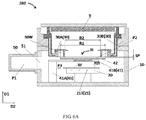
- FIG. 6A is a schematic status diagram of a sputtering process performed in a PVD chamber in some embodiments of the present disclosure
- FIG. 6B is a schematic status diagram of a sputtering process performed in a PVD chamber in some embodiments of the present disclosure
- FIG. 7 is a schematic diagram of connection status between a shielding plate and a transfer unit in some embodiments of the present disclosure.
- FIG. 8A is a schematic status diagram of a sputtering process performed in a PVD chamber in some embodiments of the present disclosure
- FIG. 8B is a schematic status diagram of a sputtering process performed in a PVD chamber in some embodiments of the present disclosure
- FIG. 9 is a schematic diagram of a deposition apparatus in some embodiments of the present disclosure.
- FIG. 10 is a schematic diagram of an operation flow of a deposition apparatus in some embodiments of the present disclosure.
- a second chamber is configured to provide a high temperature environment to allow a substrate to undergo a degas process and a sputtering process in the second chamber, so other preheating chamber and/or degas chamber can be omitted, and the effect of reducing apparatus volume and cost can be further achieved.
- a chamber body can be heated to have a high temperature environment by using a heat source provided in the chamber body, so that a degas process and a sputtering process are performed on a substrate loaded into the chamber body, thus there is no need to additionally provide a preheating chamber and/or a degas chamber, and the effect of reducing apparatus volume and cost can be further achieved.
- step is not limited to a single action, but may include a single action, operation or means, or may be a group consisting of multiple actions, operations and/or means.
- FIG. 1 is a schematic diagram of a deposition apparatus in some embodiments of the present disclosure
- FIG. 2 is a schematic diagram of an operation flow of a deposition apparatus in some embodiments of the present disclosure.
- a deposition apparatus M 1 which includes a first chamber 100 , a second chamber 200 and a third chamber 300 .
- the first chamber 100 is configured to load a substrate (not shown in FIGS. 1 and 2 ), and can thus be considered as a loading/unloading chamber, which is not limited.
- the second chamber 200 is configured to provide a high temperature environment so that a degas process and a sputtering process are performed on the loaded substrate in the second chamber 200 .
- the third chamber 300 is disposed between the first chamber 100 and the second chamber 200 and is connected to the first chamber 100 and the second chamber 200 .
- the third chamber 300 is configured to directly transfer the substrate from the first chamber 100 to the second chamber 200 via the third chamber 300 .
- the third chamber 300 may be considered as a transfer chamber, which is not limited.
- the operation flow of the deposition apparatus M 1 may include step S 1 , step S 2 and step S 3 below.
- step S 1 a substrate is loaded into the first chamber 100 of the deposition apparatus M 1 .
- step S 2 the substrate is directly transferred from the first chamber 100 to the second chamber 200 (i.e., PVD chamber) via the third chamber 300 .
- step S 3 a degas process and a sputtering process are performed on the substrate in the second chamber 200 .
- the deposition apparatus M 1 may further include a heat source (not shown in FIGS. 1 and 2 ), which is provided in the second chamber 200 and configured to provide the above high temperature environment.
- the high temperature environment of the second chamber 200 has a temperature of, for example, 400 degrees Celsius or more, and thus the heat source may be used to heat the substrate and/or the environment in the second chamber 200 before the sputtering process and/or during the sputtering process.
- the temperature in the second chamber 200 is heated above a crystallization temperature of a material layer (e.g., aluminum nitride film) to be deposited on a surface of the substrate by the heat source (for example, the temperature in the PVD chamber may be higher than 400 degrees Celsius, or preferably, may be between 400 degrees Celsius and 800 degrees Celsius, or more preferably, may be between 500 degrees Celsius and 700 degrees Celsius), the effect of degassing and/or high-temperature activating the substrate and/or the surface of the substrate can be achieved in the meanwhile.
- the second chamber 200 may also be considered as a degas and PVD chamber, which is not limited.
- temperature condition for performing PVD process can be achieved.
- the temperature may be higher than a crystallization temperature of a film formed by sputtering in the PVD process, which has a positive effect on film-formation quality in the PVD process.
- the above high temperature condition in the PVD chamber also has a positive effect on the target and chamber condition.
- the above high temperature condition can enlarge crystalline particles of the target and reduce particle related defects.
- a pasting process may be performed after a batch of sputtering is performed.
- the chamber has an environment with a temperature of more than 400 degrees Celsius, so the pasting process may be performed with low power and in a shortened time. Accordingly, the number and frequency of the pasting process can be reduced, which can shorten an overall process time and have a positive effect on life time of the target.
- the temperature is lower than 350 degrees Celsius, so crystalline particles of the target are relatively small. It results in the increase of the possibility of occurrence of particle related defects. In that case, a film on a component such as a cover ring, an upper cover, or the like is likely to crack, thus resulting in increasing particle related defects. Therefore, in the well-known PVD chamber, the pasting process needs to be performed with high power and lasts for tens of minutes, and the number and frequency of the pasting process is relatively high. This does not only increase the overall process time but also shorten life time of the target.
- the degas process and the sputtering process can be performed in the second chamber 200 , a degas chamber and/or other heating chamber can be omitted, and the effect of reducing apparatus volume and cost can be further achieved.
- the design of the deposition apparatus and the PVD chamber of the present disclosure can simplify fabrication process, and can also avoid relevant defects of the substrate caused by particles dropping on the substrate in the process of transferring the substrate heated in a heating chamber to a sputtering chamber.
- the above high temperature environment may be preferably higher than 400 degrees Celsius, which effectively allows the substrate to be degassed and/or high-temperature activated.
- the PVD process is a high temperature PVD process
- the high temperature PVD process can be implemented through continuous heating by the heat source in the second chamber 200 .
- the substrate may not need to be preheated and/or degassed in other heating chamber after being loaded into the deposition apparatus M 1 and before being subjected to the degas process and the sputtering process in the second chamber 200 .
- the third chamber 300 may not be connected to any heating chamber other than the second chamber 200 .
- the deposition apparatus M 1 does not include other heating chamber than the second chamber 200 (i.e., the PVD chamber).
- FIG. 3 is a schematic diagram of a PVD chamber in some embodiments of the present disclosure
- FIG. 4 is a schematic flow chart of a sputtering process performed in a PVD chamber in some embodiments of the present disclosure.
- the PVD chamber i.e., the second chamber 200
- the PVD chamber includes a chamber body 10 , a target T, a carrying base 20 and a heat source 21 .
- the carrying base 20 is configured to maintain a distance from the target T, and the carrying base 20 has a carrying surface 20 S facing the target T and used for carrying a substrate W.
- the heat source 21 is provided in the chamber body 10 and configured to heat the chamber body 10 to 400 degrees Celsius or more (preferably, between 400 degrees Celsius and 800 degrees Celsius, and more preferably, between 500 degrees Celsius and 700 degrees Celsius) so that a degas process and a sputtering process are performed on the substrate W.
- the heat source 21 may include a radiant heat source, which may include a plurality of heating lamps 21 T, and the substrate W may be disposed between the heat source 21 and the target T, but the present disclosure is not limited thereto.
- the PVD chamber (i.e., the second chamber 200 ) may include a transfer unit 41 and a shielding plate 42 . At least part of the transfer unit 41 is provided in the chamber body 10 , the shielding plate 42 is fixed onto the transfer unit 41 , the transfer unit 41 is configured to move the shielding plate 42 to a space between the carrying surface 20 S and the target T, and the shielding plate 42 is also between the carrying base 20 and the target T.
- the transfer unit 41 may move the shielding plate 42 to a space between the carrying surface 20 S and the target T, for example, in a rotary, translational or other suitable manner, and because the shielding plate 42 is fixed to the transfer unit 41 , the shielding plate 42 does not need to be placed on the carrying base 20 .
- the carrying base 20 can also carry thereon the substrate W to be sputtered, and hence, by having the design of the second chamber 200 (i.e., PVD chamber), a surface modification process may be performed on the target T under a condition that the substrate W has been loaded into the PVD chamber, thereby achieving the effect of shortening process time and improving production capacity.
- the second chamber 200 i.e., PVD chamber
- one or more substrates W may be placed on a tray (not shown) first, and the tray having the substrate(s) W placed thereon is then loaded into the chamber body 10 of the PVD chamber via the above first chamber 100 and third chamber 300 and placed on the carrying base 20 .
- the substrate(s) W may be directly placed on the carrying base 20 without the tray.
- the substrate W may include a sapphire substrate, silicon carbide (SiC) substrate, or a single material substrate or a composite layer material substrate formed by other suitable material, such as a silicon substrate, a silicon on insulator (SOI) substrate, a glass substrate, or a ceramic substrate, and the shielding plate 42 may be made of a high temperature resistant material such as silicon carbide (SiC), molybdenum, or the like, which are not limited.
- the chamber body 10 and components in the chamber body 10 are preferably made of metal molybdenum, low carbon stainless steel, quartz or other high temperature resistant metal or nonmetallic material, so that the above high temperature environment can be formed or other high temperature process can be performed in the chamber body 10 without any qualitative change or deformation.
- the sputtering process SR performed in the PVD chamber may include step S 11 , step S 12 , step S 13 , step S 14 , step S 15 , step S 16 and step S 17 below.
- step S 11 the substrate W is loaded into the PVD chamber.
- step S 12 a degas process is performed in the PVD chamber.
- the degas process may be implemented by using the heat source 21 to heat the chamber body 10 to form a high temperature environment, which can result in an effect of degassing and/or activating the substrate W.
- the high temperature environment may be preferably higher than a crystallization temperature of a material layer (e.g., aluminum nitride film) to be deposited on a surface of the substrate (for example, the temperature in the PVD chamber may be higher than 400 degrees Celsius, or preferably, may be between 400 degrees Celsius and 800 degrees Celsius, which is not limited).
- a material layer e.g., aluminum nitride film
- step S 13 the transfer unit 41 is used to move the shielding plate 42 to a space between the carrying surface 20 S and the target T.
- step S 14 a surface modification process is performed on the target.
- step S 15 the transfer unit 41 is used to move the shielding plate 42 away.
- step S 16 sputtering is performed on the substrate W using the target T in the chamber body 10 to form a film on the substrate W.
- step S 17 the substrate W having the film formed thereon is carried out of the PVD chamber.
- the shielding plate 42 between the carrying surface 20 S and the target T can avoid the material of the target T from forming on the substrate W.
- the action of forming the high temperature environment in the chamber body 10 by the heat source 21 may be regarded as a heating process, and at least part of the heating process may be performed simultaneously with the surface modification process of the target T, thus achieving the effect of shortening the overall process time.
- the heat source 21 in the second chamber 200 may be used to heat continuously to implement the high temperature PVD process.
- the heat source 21 may be provided within the chamber body 10 and heat the second chamber 200 to 400 degrees Celsius or more, so the heat source 21 may be configured to control the temperature in the chamber body 10 .
- the heat source 21 may be used to heat the chamber body 10 and/or the substrate W to achieve the degas effect and/or reach the process temperature required for the PCV process.
- the above sputtering process SR performed in the PVD chamber is illustrative only, but the present disclosure is not limited thereto, other additional step that is required may be performed before, after and/or in the sputtering process SR, and the steps in the sputtering process SR may be replaced, omitted, or changed in sequence in other embodiments.
- the above deposition apparatus and PVD chamber may be used to form a non-metallic film, a metal film or a metal compound film such as an aluminum nitride (AlN) film, which is not limited.
- the second chamber 200 may be an aluminum nitride PVD chamber and configured to form an aluminum nitride film on the substrate W.
- FIG. 5 is a schematic diagram of a PVD chamber in some embodiments of the present disclosure.
- the PVD chamber 201 may further include a shielding unit 30 provided in the chamber body 10 and between the target T and the carrying base 20 .
- the shielding plate 42 moves to a space between the carrying surface 20 S and the target T, the shielding plate 42 is also between the carrying base 20 and the shielding unit 30 .
- the carrying base 20 and the shielding unit 30 may be provided correspondingly in a first direction D 1 , which may be considered as a vertical direction, but the present disclosure is not limited thereto.
- the shielding unit 30 is provided between the carrying base 20 and the target T in the first direction D 1 .
- the shielding plate 42 is fixed to the transfer unit 41 , the transfer unit 41 is configured to move the shielding plate 42 between a temporary position P 1 and a shielding position P 2 in a second direction D 2 , and the shielding plate 42 is between the carrying surface 20 S and the target T and between the carrying surface 20 S and the shielding unit 30 when being moved to the shielding position P 2 .
- the second direction D 1 may be considered as a horizontal direction, which is not limited.
- the transfer unit 41 may move the shielding plate 42 to a space between the carrying surface 20 S and the target T, for example, in a rotary, translational or other suitable manner, i.e., move the shielding plate 42 between the temporary position P 1 and the shielding position P 2 in the second direction D 2 , which is not limited.
- the PVD chamber 201 may further include a plurality of ejector pins 22 provided on the carrying base 20 and configured to lift the substrate W from the surface of the carrying base 20 .
- the ejector pins 22 may include temperature measuring ejector pins used for detecting a temperature in the chamber body 10 and/or a temperature of the substrate W, which is not limited.
- the shielding plate 42 may have an adhesive surface, at least part of which faces the target T, and the adhesive surface may include a rough surface or an adhesive surface formed by an appropriate surface treatment such as sandblasting, melting, surface roughening or the like to increase bonding capacity between the shielding plate 42 and material of the target T, further enable an upper surface of the shielding plate 42 to adsorb more material falling from target T, and achieve the effect of enhancing the shielding effect of the shielding plate 42 .
- an appropriate surface treatment such as sandblasting, melting, surface roughening or the like
- FIGS. 6A, 6B and 7 are schematic status diagrams of a sputtering process performed in a PVD chamber in some embodiments of the present disclosure
- FIG. 7 is a schematic diagram of connection status between a shielding plate and a transfer unit in some embodiments of the present disclosure.
- the shielding plate 42 may be moved to the space between the carrying surface 20 S and the target T, or may be transferred to the shielding position P 2 above the substrate W, by using the transfer unit 41 ; alternatively, as shown in FIG. 6B , the shielding plate 42 is moved to the temporary position P 1 formed by a shielding plate depository 50 through a port 51 by using the transfer unit 41 .
- sealing treatment may be performed between the shielding plate depository 50 and the chamber body 10 ; considering vacuum integrity between the shielding plate depository 50 and the chamber body 10 , the shielding plate depository 50 and the chamber body 10 may be connected through welding or formed integrally.
- the transfer unit 41 may move the shielding plate 42 to the space between the carrying surface 20 S and the target T in a rotary or other suitable manner, or move the shielding plate 42 between the temporary position P 1 and the shielding position P 2 in the second direction D 2 .
- the structure of the transfer unit 41 may include a rotary axis 41 A and a support plate 41 B, the shielding plate 42 may be fixed to an upper surface of the support plate 41 B, and the rotary axis 41 A is connected to the support plate 41 B.
- the rotary axis 41 A may drive the support plate 41 B to rotate clockwise or counter-clockwise by a preset angle, to move the shielding plate 42 to the shielding position P 2 or the temporary position P 1 .
- the shielding plate 42 may be fixed to the transfer unit 41 through a fixing component 43 .
- the fixing component 43 may include a screw, a rivet, an adhesive material, or other suitable fixing component, and is used for fixing the shielding plate 42 to the support plate 41 B of the transfer unit 41 .
- other detachable manner or undetachable manner e.g., welding
- the shielding unit 30 has an opening H, and an area of the shielding plate 42 (e.g., a projected area of the shielding plate 42 in the first direction D 1 ) is larger than that of the opening H of the shielding unit 30 , so as to ensure the shielding effect of the shielding plate 42 .
- the shielding unit 30 may include a shielding ring 30 A and an annular housing 30 B for supporting the shielding ring 30 A, and an internal surface 30 W of one end of the shielding ring 30 A proximal to the carrying surface 20 S defines the opening H, which is not limited.
- the shielding plate 42 When the shielding plate 42 is moved to the shielding position P 2 (between the carrying surface 20 S and the shielding unit 30 ), there is a spacing distance SP between the shielding plate 42 and the shielding unit 30 in the first direction D 1 , to ensure that the shielding plate 42 can be smoothly moved in the second direction D 2 and target material sputtered off the target T cannot be sputtered to the substrate W through the gap between the shielding unit 30 and the shielding plate 42 .
- the spacing distance SP may be between 2 mm and 4 mm, which is not limited.
- an outer diameter R 1 of the shielding plate 42 is preferably larger than an inner diameter R 2 of the shielding ring 30 A, so as to ensure that material of the target T can only be sputtered towards a side wall of the chamber body 10 but not onto the substrate W even if it has passed through the gap between the shielding ring 30 A and the shielding plate 42 .
- the above inner diameter R 2 may be considered as a diameter of the opening H, and the outer diameter R 1 of the shielding plate 42 may be preferably larger than the inner diameter R 2 of the shielding ring 30 A by 20 mm to 30 mm, which is not limited.
- the shielding plate 42 when the shielding plate 42 is moved to the temporary position P 1 , the substrate W on the carrying base 20 may rise to a process position P 4 with the aid of the carrying base 20 , at this point, the shielding ring 30 A may be held up from the annular housing 30 B so that the shielding ring 30 A presses, under its own gravity, against an edge portion of the substrate W to sputter the substrate W using the target T.
- the shielding plate 42 When the shielding plate 42 is at the temporary position P 1 , a portion of the shielding plate 42 is moved into a space contained by the shielding plate depository 50 via the port 51 , and the remaining portion of the shielding plate 42 is shifted towards a peripheral direction of the chamber body 10 until it is out of a rising path of the substrate W and the carrying base 20 , thus ensuring that the substrate W can rise to the process position P 4 smoothly.
- FIGS. 8A and 8B are schematic status diagrams of a sputtering process performed in a PVD chamber in some embodiments of the present disclosure.
- the shielding plate 42 may be moved to the space between the carrying surface 20 S and the target T, in other words, transferred to the shielding position P 2 above the substrate W, by using the transfer unit 41 ; or, as shown in FIG. 8B , the shielding plate 42 may be moved to the temporary position P 1 formed by the shielding plate depository 50 via the port 5 by using the transfer unit 41 .
- FIGS. 8A and 8B are schematic status diagrams of a sputtering process performed in a PVD chamber in some embodiments of the present disclosure.
- the shielding plate 42 may be moved to the space between the carrying surface 20 S and the target T, in other words, transferred to the shielding position P 2 above the substrate W, by using the transfer unit 41 ; or, as shown in FIG. 8B , the shielding plate 42 may be moved to the temporary position P 1 formed by the shielding plate de
- the transfer unit 41 may move the shielding plate 42 to the space between the carrying surface 20 S and the target T in a transitional manner, in other words, move the shielding plate 42 between the temporary position P 1 and the shielding position P 2 in the second direction D 2 .
- the transfer unit 41 may include a mechanical arm 41 C used for carrying the shielding plate 42 and provided in the space formed by the shielding plate depository 50 , and the mechanical arm 41 C may stretch into the interior of the chamber body 10 via the port 51 , or is retracted into the space formed by the shielding plate depository 50 from the interior of the chamber body 10 , thus moving the shielding plate 42 to the shielding position P 2 or the temporary position P 1 .
- the mechanical arm 41 C may be formed by a plurality of connected cantilevers, which achieve horizontal telescopic action in the second direction D 2 through folding or unfolding, but the present disclosure is not limited thereto.
- Other mechanical arm having other configuration or other structure that can be used to achieve horizontal telescopic action in the second direction D 2 should be encompassed in the scope of the present disclosure.
- FIG. 9 is a schematic diagram of a deposition apparatus in some embodiments of the present disclosure
- FIG. 10 is a schematic diagram of an operation flow of a deposition apparatus in some embodiments of the present disclosure.
- some embodiments of the present disclosure provide a deposition apparatus M 2 , which differs from the above deposition apparatus M 1 shown in FIG. 1 in that the deposition apparatus M 2 further includes a fourth chamber 400 connected to the third chamber 300 and configured to perform a cooling process in which the cooling operation is performed on the substrate having been subjected to the degas process and the sputtering process in the second chamber 200 .
- the operation flow of the deposition apparatus M 2 may include step S 1 , step S 2 , step S 3 and step S 4 shown in FIG. 10 .
- step S 1 the substrate is loaded into the first chamber 100 of the deposition apparatus M 2 .
- step S 2 the substrate is directly transferred from the first chamber 100 to the second chamber 200 via the third chamber 300 .
- step S 3 a degas process and a sputtering process are performed on the substrate in the second chamber 200 .
- step S 4 the substrate having been subjected to the degas process and the sputtering process is carried out of the second chamber 200 , and transferred to the fourth chamber 400 via the third chamber 300 to undergo the cooling process. Further, after the temperature of the substrate is lowered to a predetermined temperature in the fourth chamber 400 , the substrate may be taken out of the fourth chamber 400 and then carried out of the deposition apparatus M 2 sequentially via the third chamber 300 and the first chamber 100 .
- the PVD chamber is configured to heat the chamber body into a high temperature environment, so the degas process and the sputtering process can be performed on the substrate in the PVD chamber.
- the substrate may be directly transferred from the loading/unloading chamber to the PVD chamber to perform the degas process and the sputtering process on the substrate, thereby omitting a preheating/degas chamber and achieving the effect of reducing apparatus volume and cost.
- fabrication process can be simplified, and the problem that particles may fall on the substrate in the process of transferring the substrate heated in other heating chamber to the PVD chamber may be avoided.
- a heat source may be provided in the chamber body to heat the chamber body into a high temperature environment for performing the degas process and the sputtering process on the substrate loaded into the chamber body.
- the shielding plate is fixed to the transfer unit, and the transfer unit moves the shielding plate to the space between the carrying surface of the carrying base and the target, so that the carrying base can still carry thereon the substrate to be sputtered when the shielding plate is at the shielding position, and in this way, the target can be cleaned under the condition that the substrate has been loaded, and the effect of shortening process time and improving production capacity can be further achieved.
- the substrate below the shielding plate can undergo the heating process at the same time, thus degassing and/or high-temperature activating the substrate, shortening the overall process time and promoting the production capacity.
Landscapes
- Chemical & Material Sciences (AREA)
- Engineering & Computer Science (AREA)
- Chemical Kinetics & Catalysis (AREA)
- Materials Engineering (AREA)
- Mechanical Engineering (AREA)
- Metallurgy (AREA)
- Organic Chemistry (AREA)
- Physics & Mathematics (AREA)
- Plasma & Fusion (AREA)
- Analytical Chemistry (AREA)
- Physical Vapour Deposition (AREA)
Abstract
Description
Claims (20)
Applications Claiming Priority (3)
| Application Number | Priority Date | Filing Date | Title |
|---|---|---|---|
| CN201610407585.8 | 2016-06-12 | ||
| CN201610407585.8A CN107488832B (en) | 2016-06-12 | 2016-06-12 | Depositing device and physical vapor deposition chamber |
| PCT/CN2016/101565 WO2017215154A1 (en) | 2016-06-12 | 2016-10-09 | Deposition device and physical vapour deposition chamber |
Publications (2)
| Publication Number | Publication Date |
|---|---|
| US20180247799A1 US20180247799A1 (en) | 2018-08-30 |
| US10984994B2 true US10984994B2 (en) | 2021-04-20 |
Family
ID=60642968
Family Applications (1)
| Application Number | Title | Priority Date | Filing Date |
|---|---|---|---|
| US15/551,493 Active 2036-12-14 US10984994B2 (en) | 2016-06-12 | 2016-10-09 | Deposition apparatus and physical vapor deposition chamber |
Country Status (7)
| Country | Link |
|---|---|
| US (1) | US10984994B2 (en) |
| KR (1) | KR102078326B1 (en) |
| CN (1) | CN107488832B (en) |
| MY (1) | MY193979A (en) |
| SG (1) | SG11201810530YA (en) |
| TW (1) | TWI652364B (en) |
| WO (1) | WO2017215154A1 (en) |
Families Citing this family (13)
| Publication number | Priority date | Publication date | Assignee | Title |
|---|---|---|---|---|
| CN110344018B (en) * | 2018-04-08 | 2020-09-08 | 北京七星华创集成电路装备有限公司 | A multi-cathode continuous coating chamber |
| KR102699890B1 (en) * | 2018-04-18 | 2024-08-29 | 어플라이드 머티어리얼스, 인코포레이티드 | Two-piece shutter disc assembly with self-centering feature |
| CN111986976B (en) * | 2019-05-22 | 2022-04-22 | 北京北方华创微电子装备有限公司 | Process chamber and semiconductor processing equipment |
| US11492700B2 (en) | 2019-10-18 | 2022-11-08 | Taiwan Semiconductor Manufacturing Co. | Shutter disk having lamp, power, and/or gas modules arranged at the first side of the shutter disk of thin film deposition chamber |
| CN110938807B (en) * | 2019-11-26 | 2022-10-21 | 北京北方华创微电子装备有限公司 | Control method and system for returning wafer of PVD sputtering equipment to disc according to specified path |
| FR3116151A1 (en) * | 2020-11-10 | 2022-05-13 | Commissariat A L'energie Atomique Et Aux Energies Alternatives | METHOD FOR FORMING A USEFUL SUBSTRATE TRAPPING STRUCTURE |
| CN114369804B (en) * | 2022-01-11 | 2023-10-13 | 北京北方华创微电子装备有限公司 | Thin film deposition method |
| CN114318286B (en) * | 2022-01-27 | 2025-03-28 | 北京青禾晶元半导体科技有限责任公司 | A composite substrate preparation device and a composite substrate preparation method |
| KR20240151186A (en) * | 2022-02-14 | 2024-10-17 | 어플라이드 머티어리얼스, 인코포레이티드 | Device and method for manufacturing PVD perovskite films |
| CN115074692B (en) * | 2022-06-24 | 2023-10-13 | 北京北方华创微电子装备有限公司 | Semiconductor process equipment and process chamber thereof |
| CN116695086B (en) * | 2023-06-30 | 2024-04-16 | 北京北方华创微电子装备有限公司 | Process chamber, semiconductor process equipment and thin film deposition method |
| CN121320866A (en) * | 2024-07-09 | 2026-01-13 | 北京北方华创微电子装备有限公司 | Semiconductor process chambers and semiconductor process equipment |
| CN119465019B (en) * | 2025-01-13 | 2025-04-18 | 上海陛通半导体能源科技股份有限公司 | A device for rapidly cooling semiconductor components after high-temperature degassing |
Citations (20)
| Publication number | Priority date | Publication date | Assignee | Title |
|---|---|---|---|---|
| US5131460A (en) * | 1991-10-24 | 1992-07-21 | Applied Materials, Inc. | Reducing particulates during semiconductor fabrication |
| JPH0711442A (en) | 1993-06-28 | 1995-01-13 | Fuji Electric Co Ltd | Sputtering equipment for semiconductor device manufacturing |
| US5624536A (en) * | 1994-06-08 | 1997-04-29 | Tel Varian Limited | Processing apparatus with collimator exchange device |
| US5925227A (en) * | 1996-05-21 | 1999-07-20 | Anelva Corporation | Multichamber sputtering apparatus |
| US6110821A (en) | 1998-01-27 | 2000-08-29 | Applied Materials, Inc. | Method for forming titanium silicide in situ |
| US6132805A (en) * | 1998-10-20 | 2000-10-17 | Cvc Products, Inc. | Shutter for thin-film processing equipment |
| JP2002302763A (en) | 2001-04-05 | 2002-10-18 | Anelva Corp | Sputtering equipment |
| JP2004277773A (en) | 2003-03-13 | 2004-10-07 | Murata Mfg Co Ltd | Inline sputtering system |
| US20050227120A1 (en) | 2004-04-12 | 2005-10-13 | Hitachi Global Storage Technologies Netherlands B.V. | Magnetic recording medium and magnetic recording apparatus |
| CN101542013A (en) | 2007-06-04 | 2009-09-23 | 佳能安内华股份有限公司 | Film forming apparatus |
| CN101674893A (en) | 2007-05-09 | 2010-03-17 | 应用材料股份有限公司 | Transfer chamber for shutter disk storage with vacuum extension chamber |
| CN201648508U (en) | 2010-03-05 | 2010-11-24 | 凌嘉科技股份有限公司 | Horizontal step-type sputtering device |
| JP2011108603A (en) * | 2009-11-20 | 2011-06-02 | Ulvac Japan Ltd | Thin film lithium secondary battery, and forming method of thin film lithium secondary battery |
| WO2011077653A1 (en) | 2009-12-25 | 2011-06-30 | キヤノンアネルバ株式会社 | Method for manufacturing electronic device, and sputtering apparatus |
| US20110240462A1 (en) * | 2010-04-02 | 2011-10-06 | Semiconductor Energy Laboratory Co., Ltd. | Deposition apparatus and method for manufacturing semiconductor device |
| CN102560388A (en) | 2010-12-09 | 2012-07-11 | 北京北方微电子基地设备工艺研究中心有限责任公司 | Magnetic control sputtering equipment |
| CN103173730A (en) | 2011-12-23 | 2013-06-26 | 北京北方微电子基地设备工艺研究中心有限责任公司 | Magnetron sputtering apparatus and process |
| CN103668095A (en) | 2013-12-26 | 2014-03-26 | 广东工业大学 | High-power pulse plasma reinforced composite magnetron sputtering deposition device and application method thereof |
| US20140102878A1 (en) * | 2004-12-08 | 2014-04-17 | Hongmei Zhang | DEPOSITION OF LiCoO2 |
| CN104024467A (en) | 2011-12-22 | 2014-09-03 | 佳能安内华股份有限公司 | Deposition Method of SrRuO3 Film |
-
2016
- 2016-06-12 CN CN201610407585.8A patent/CN107488832B/en active Active
- 2016-07-29 TW TW105124061A patent/TWI652364B/en active
- 2016-10-09 SG SG11201810530YA patent/SG11201810530YA/en unknown
- 2016-10-09 MY MYPI2018002526A patent/MY193979A/en unknown
- 2016-10-09 US US15/551,493 patent/US10984994B2/en active Active
- 2016-10-09 WO PCT/CN2016/101565 patent/WO2017215154A1/en not_active Ceased
- 2016-10-09 KR KR1020177035747A patent/KR102078326B1/en active Active
Patent Citations (22)
| Publication number | Priority date | Publication date | Assignee | Title |
|---|---|---|---|---|
| US5131460A (en) * | 1991-10-24 | 1992-07-21 | Applied Materials, Inc. | Reducing particulates during semiconductor fabrication |
| JPH0711442A (en) | 1993-06-28 | 1995-01-13 | Fuji Electric Co Ltd | Sputtering equipment for semiconductor device manufacturing |
| US5624536A (en) * | 1994-06-08 | 1997-04-29 | Tel Varian Limited | Processing apparatus with collimator exchange device |
| US5925227A (en) * | 1996-05-21 | 1999-07-20 | Anelva Corporation | Multichamber sputtering apparatus |
| KR100270459B1 (en) | 1996-05-21 | 2000-12-01 | 니시히라 쥰지 | Multichamber Sputtering Device |
| US6110821A (en) | 1998-01-27 | 2000-08-29 | Applied Materials, Inc. | Method for forming titanium silicide in situ |
| US6132805A (en) * | 1998-10-20 | 2000-10-17 | Cvc Products, Inc. | Shutter for thin-film processing equipment |
| JP2002302763A (en) | 2001-04-05 | 2002-10-18 | Anelva Corp | Sputtering equipment |
| JP2004277773A (en) | 2003-03-13 | 2004-10-07 | Murata Mfg Co Ltd | Inline sputtering system |
| US20050227120A1 (en) | 2004-04-12 | 2005-10-13 | Hitachi Global Storage Technologies Netherlands B.V. | Magnetic recording medium and magnetic recording apparatus |
| US20140102878A1 (en) * | 2004-12-08 | 2014-04-17 | Hongmei Zhang | DEPOSITION OF LiCoO2 |
| CN101674893A (en) | 2007-05-09 | 2010-03-17 | 应用材料股份有限公司 | Transfer chamber for shutter disk storage with vacuum extension chamber |
| CN101542013A (en) | 2007-06-04 | 2009-09-23 | 佳能安内华股份有限公司 | Film forming apparatus |
| JP2011108603A (en) * | 2009-11-20 | 2011-06-02 | Ulvac Japan Ltd | Thin film lithium secondary battery, and forming method of thin film lithium secondary battery |
| WO2011077653A1 (en) | 2009-12-25 | 2011-06-30 | キヤノンアネルバ株式会社 | Method for manufacturing electronic device, and sputtering apparatus |
| CN201648508U (en) | 2010-03-05 | 2010-11-24 | 凌嘉科技股份有限公司 | Horizontal step-type sputtering device |
| US20110240462A1 (en) * | 2010-04-02 | 2011-10-06 | Semiconductor Energy Laboratory Co., Ltd. | Deposition apparatus and method for manufacturing semiconductor device |
| CN102560388A (en) | 2010-12-09 | 2012-07-11 | 北京北方微电子基地设备工艺研究中心有限责任公司 | Magnetic control sputtering equipment |
| CN104024467A (en) | 2011-12-22 | 2014-09-03 | 佳能安内华股份有限公司 | Deposition Method of SrRuO3 Film |
| US20140360863A1 (en) | 2011-12-22 | 2014-12-11 | Canon Anelva Corporation | SrRuO3 FILM DEPOSITION METHOD |
| CN103173730A (en) | 2011-12-23 | 2013-06-26 | 北京北方微电子基地设备工艺研究中心有限责任公司 | Magnetron sputtering apparatus and process |
| CN103668095A (en) | 2013-12-26 | 2014-03-26 | 广东工业大学 | High-power pulse plasma reinforced composite magnetron sputtering deposition device and application method thereof |
Non-Patent Citations (2)
| Title |
|---|
| Machine Translation JP 2011-108603 dated Jun. 2011. (Year: 2011). * |
| The World Intellectual Property Organization (WIPO) International Search Report for PCT/CN2016/101565 dated Mar. 15, 2017 5 Pages. |
Also Published As
| Publication number | Publication date |
|---|---|
| TWI652364B (en) | 2019-03-01 |
| MY193979A (en) | 2022-11-04 |
| CN107488832A (en) | 2017-12-19 |
| KR102078326B1 (en) | 2020-04-07 |
| US20180247799A1 (en) | 2018-08-30 |
| SG11201810530YA (en) | 2018-12-28 |
| KR20180018554A (en) | 2018-02-21 |
| TW201742939A (en) | 2017-12-16 |
| CN107488832B (en) | 2019-11-29 |
| WO2017215154A1 (en) | 2017-12-21 |
Similar Documents
| Publication | Publication Date | Title |
|---|---|---|
| US10984994B2 (en) | Deposition apparatus and physical vapor deposition chamber | |
| CN102150251B (en) | Substrate holding member, substrate processing apparatus, and substrate processing method | |
| KR101841201B1 (en) | Process chamber and semiconductor processing apparatus | |
| CN104428885B (en) | Two-Piece Baffled Tray Assembly for Substrate Processing Chambers | |
| TWI752283B (en) | Shutter disk assembly, semiconductor processing apparatus and method | |
| TW202003892A (en) | Pre-clean chamber with integrated shutter garage | |
| US8709218B2 (en) | Vacuum processing apparatus, vacuum processing method, and electronic device manufacturing method | |
| CN1603455A (en) | Thin-film deposition system | |
| KR101970866B1 (en) | Vacuum treatment device | |
| JPWO2019082868A1 (en) | Substrate processing equipment, support pins | |
| US10435784B2 (en) | Thermally optimized rings | |
| JP2001335927A (en) | Sputtering equipment | |
| WO2009157228A1 (en) | Sputtering apparatus, sputtering method and light emitting element manufacturing method | |
| TWM610249U (en) | Thin-film deposition apparatus | |
| CN114318284B (en) | Film forming device | |
| TWI727610B (en) | Electrostatic chuck and its plasma processing device | |
| TWI860323B (en) | Substrate carrier | |
| CN115995418B (en) | Substrate mounting method and substrate mounting mechanism | |
| TWI722944B (en) | Thin-film deposition apparatus and thin-film deposition method | |
| CN115725947B (en) | Substrate supporting and fixing mechanism and thin film deposition equipment |
Legal Events
| Date | Code | Title | Description |
|---|---|---|---|
| AS | Assignment |
Owner name: BEIJING NAURA MICROELECTRONICS EQUIPMENT CO., LTD., CHINA Free format text: ASSIGNMENT OF ASSIGNORS INTEREST;ASSIGNORS:ZHANG, JUN;DONG, BOYU;ZHAO, JINRONG;AND OTHERS;SIGNING DATES FROM 20170706 TO 20170731;REEL/FRAME:043576/0287 Owner name: BEIJING NAURA MICROELECTRONICS EQUIPMENT CO., LTD. Free format text: ASSIGNMENT OF ASSIGNORS INTEREST;ASSIGNORS:ZHANG, JUN;DONG, BOYU;ZHAO, JINRONG;AND OTHERS;SIGNING DATES FROM 20170706 TO 20170731;REEL/FRAME:043576/0287 |
|
| STPP | Information on status: patent application and granting procedure in general |
Free format text: NON FINAL ACTION MAILED |
|
| STPP | Information on status: patent application and granting procedure in general |
Free format text: RESPONSE TO NON-FINAL OFFICE ACTION ENTERED AND FORWARDED TO EXAMINER |
|
| STPP | Information on status: patent application and granting procedure in general |
Free format text: FINAL REJECTION MAILED |
|
| STPP | Information on status: patent application and granting procedure in general |
Free format text: ADVISORY ACTION MAILED |
|
| STPP | Information on status: patent application and granting procedure in general |
Free format text: DOCKETED NEW CASE - READY FOR EXAMINATION |
|
| STPP | Information on status: patent application and granting procedure in general |
Free format text: NON FINAL ACTION MAILED |
|
| STPP | Information on status: patent application and granting procedure in general |
Free format text: RESPONSE TO NON-FINAL OFFICE ACTION ENTERED AND FORWARDED TO EXAMINER |
|
| STPP | Information on status: patent application and granting procedure in general |
Free format text: FINAL REJECTION MAILED |
|
| STPP | Information on status: patent application and granting procedure in general |
Free format text: RESPONSE AFTER FINAL ACTION FORWARDED TO EXAMINER |
|
| STPP | Information on status: patent application and granting procedure in general |
Free format text: ADVISORY ACTION MAILED |
|
| STPP | Information on status: patent application and granting procedure in general |
Free format text: RESPONSE TO NON-FINAL OFFICE ACTION ENTERED AND FORWARDED TO EXAMINER |
|
| STPP | Information on status: patent application and granting procedure in general |
Free format text: NOTICE OF ALLOWANCE MAILED -- APPLICATION RECEIVED IN OFFICE OF PUBLICATIONS |
|
| STPP | Information on status: patent application and granting procedure in general |
Free format text: PUBLICATIONS -- ISSUE FEE PAYMENT RECEIVED |
|
| STPP | Information on status: patent application and granting procedure in general |
Free format text: PUBLICATIONS -- ISSUE FEE PAYMENT VERIFIED |
|
| STCF | Information on status: patent grant |
Free format text: PATENTED CASE |
|
| MAFP | Maintenance fee payment |
Free format text: PAYMENT OF MAINTENANCE FEE, 4TH YEAR, LARGE ENTITY (ORIGINAL EVENT CODE: M1551); ENTITY STATUS OF PATENT OWNER: LARGE ENTITY Year of fee payment: 4 |