US10971069B2 - Pixel driving circuit, driving method thereof and display device - Google Patents

Pixel driving circuit, driving method thereof and display device Download PDF

Info

Publication number
US10971069B2
US10971069B2 US16/616,234 US201916616234A US10971069B2 US 10971069 B2 US10971069 B2 US 10971069B2 US 201916616234 A US201916616234 A US 201916616234A US 10971069 B2 US10971069 B2 US 10971069B2
Authority
US
United States
Prior art keywords
light
electrode
emitting
unit
driving transistor
Prior art date
Legal status (The legal status is an assumption and is not a legal conclusion. Google has not performed a legal analysis and makes no representation as to the accuracy of the status listed.)
Active
Application number
US16/616,234
Other versions
US20200090591A1 (en
Inventor
Tieshi WANG
Kuanjun PENG
Wei Qin
Chengchung YANG
Xueling GAO
Xiaolong Li
Zhiqiang Xu
Yan Wei
Shengnan LI
Current Assignee (The listed assignees may be inaccurate. Google has not performed a legal analysis and makes no representation or warranty as to the accuracy of the list.)
BOE Technology Group Co Ltd
Original Assignee
BOE Technology Group Co Ltd
Priority date (The priority date is an assumption and is not a legal conclusion. Google has not performed a legal analysis and makes no representation as to the accuracy of the date listed.)
Filing date
Publication date
Application filed by BOE Technology Group Co Ltd filed Critical BOE Technology Group Co Ltd
Assigned to BOE TECHNOLOGY GROUP CO., LTD. reassignment BOE TECHNOLOGY GROUP CO., LTD. ASSIGNMENT OF ASSIGNORS INTEREST (SEE DOCUMENT FOR DETAILS). Assignors: LI, Shengnan, GAO, Xueling, LI, XIAOLONG, Peng, Kuanjun, QIN, WEI, WANG, Tieshi, XU, ZHIQIANG, YANG, Chengchung, WEI, YAN
Publication of US20200090591A1 publication Critical patent/US20200090591A1/en
Application granted granted Critical
Publication of US10971069B2 publication Critical patent/US10971069B2/en
Active legal-status Critical Current
Anticipated expiration legal-status Critical

Links

Images

Classifications

    • GPHYSICS
    • G09EDUCATION; CRYPTOGRAPHY; DISPLAY; ADVERTISING; SEALS
    • G09GARRANGEMENTS OR CIRCUITS FOR CONTROL OF INDICATING DEVICES USING STATIC MEANS TO PRESENT VARIABLE INFORMATION
    • G09G3/00Control arrangements or circuits, of interest only in connection with visual indicators other than cathode-ray tubes
    • G09G3/20Control arrangements or circuits, of interest only in connection with visual indicators other than cathode-ray tubes for presentation of an assembly of a number of characters, e.g. a page, by composing the assembly by combination of individual elements arranged in a matrix no fixed position being assigned to or needed to be assigned to the individual characters or partial characters
    • G09G3/22Control arrangements or circuits, of interest only in connection with visual indicators other than cathode-ray tubes for presentation of an assembly of a number of characters, e.g. a page, by composing the assembly by combination of individual elements arranged in a matrix no fixed position being assigned to or needed to be assigned to the individual characters or partial characters using controlled light sources
    • G09G3/30Control arrangements or circuits, of interest only in connection with visual indicators other than cathode-ray tubes for presentation of an assembly of a number of characters, e.g. a page, by composing the assembly by combination of individual elements arranged in a matrix no fixed position being assigned to or needed to be assigned to the individual characters or partial characters using controlled light sources using electroluminescent panels
    • G09G3/32Control arrangements or circuits, of interest only in connection with visual indicators other than cathode-ray tubes for presentation of an assembly of a number of characters, e.g. a page, by composing the assembly by combination of individual elements arranged in a matrix no fixed position being assigned to or needed to be assigned to the individual characters or partial characters using controlled light sources using electroluminescent panels semiconductive, e.g. using light-emitting diodes [LED]
    • G09G3/3208Control arrangements or circuits, of interest only in connection with visual indicators other than cathode-ray tubes for presentation of an assembly of a number of characters, e.g. a page, by composing the assembly by combination of individual elements arranged in a matrix no fixed position being assigned to or needed to be assigned to the individual characters or partial characters using controlled light sources using electroluminescent panels semiconductive, e.g. using light-emitting diodes [LED] organic, e.g. using organic light-emitting diodes [OLED]
    • G09G3/3225Control arrangements or circuits, of interest only in connection with visual indicators other than cathode-ray tubes for presentation of an assembly of a number of characters, e.g. a page, by composing the assembly by combination of individual elements arranged in a matrix no fixed position being assigned to or needed to be assigned to the individual characters or partial characters using controlled light sources using electroluminescent panels semiconductive, e.g. using light-emitting diodes [LED] organic, e.g. using organic light-emitting diodes [OLED] using an active matrix
    • G09G3/3258Control arrangements or circuits, of interest only in connection with visual indicators other than cathode-ray tubes for presentation of an assembly of a number of characters, e.g. a page, by composing the assembly by combination of individual elements arranged in a matrix no fixed position being assigned to or needed to be assigned to the individual characters or partial characters using controlled light sources using electroluminescent panels semiconductive, e.g. using light-emitting diodes [LED] organic, e.g. using organic light-emitting diodes [OLED] using an active matrix with pixel circuitry controlling the voltage across the light-emitting element
    • GPHYSICS
    • G09EDUCATION; CRYPTOGRAPHY; DISPLAY; ADVERTISING; SEALS
    • G09GARRANGEMENTS OR CIRCUITS FOR CONTROL OF INDICATING DEVICES USING STATIC MEANS TO PRESENT VARIABLE INFORMATION
    • G09G3/00Control arrangements or circuits, of interest only in connection with visual indicators other than cathode-ray tubes
    • G09G3/20Control arrangements or circuits, of interest only in connection with visual indicators other than cathode-ray tubes for presentation of an assembly of a number of characters, e.g. a page, by composing the assembly by combination of individual elements arranged in a matrix no fixed position being assigned to or needed to be assigned to the individual characters or partial characters
    • G09G3/22Control arrangements or circuits, of interest only in connection with visual indicators other than cathode-ray tubes for presentation of an assembly of a number of characters, e.g. a page, by composing the assembly by combination of individual elements arranged in a matrix no fixed position being assigned to or needed to be assigned to the individual characters or partial characters using controlled light sources
    • G09G3/30Control arrangements or circuits, of interest only in connection with visual indicators other than cathode-ray tubes for presentation of an assembly of a number of characters, e.g. a page, by composing the assembly by combination of individual elements arranged in a matrix no fixed position being assigned to or needed to be assigned to the individual characters or partial characters using controlled light sources using electroluminescent panels
    • G09G3/32Control arrangements or circuits, of interest only in connection with visual indicators other than cathode-ray tubes for presentation of an assembly of a number of characters, e.g. a page, by composing the assembly by combination of individual elements arranged in a matrix no fixed position being assigned to or needed to be assigned to the individual characters or partial characters using controlled light sources using electroluminescent panels semiconductive, e.g. using light-emitting diodes [LED]
    • G09G3/3208Control arrangements or circuits, of interest only in connection with visual indicators other than cathode-ray tubes for presentation of an assembly of a number of characters, e.g. a page, by composing the assembly by combination of individual elements arranged in a matrix no fixed position being assigned to or needed to be assigned to the individual characters or partial characters using controlled light sources using electroluminescent panels semiconductive, e.g. using light-emitting diodes [LED] organic, e.g. using organic light-emitting diodes [OLED]
    • G09G3/3225Control arrangements or circuits, of interest only in connection with visual indicators other than cathode-ray tubes for presentation of an assembly of a number of characters, e.g. a page, by composing the assembly by combination of individual elements arranged in a matrix no fixed position being assigned to or needed to be assigned to the individual characters or partial characters using controlled light sources using electroluminescent panels semiconductive, e.g. using light-emitting diodes [LED] organic, e.g. using organic light-emitting diodes [OLED] using an active matrix
    • G09G3/3233Control arrangements or circuits, of interest only in connection with visual indicators other than cathode-ray tubes for presentation of an assembly of a number of characters, e.g. a page, by composing the assembly by combination of individual elements arranged in a matrix no fixed position being assigned to or needed to be assigned to the individual characters or partial characters using controlled light sources using electroluminescent panels semiconductive, e.g. using light-emitting diodes [LED] organic, e.g. using organic light-emitting diodes [OLED] using an active matrix with pixel circuitry controlling the current through the light-emitting element
    • GPHYSICS
    • G09EDUCATION; CRYPTOGRAPHY; DISPLAY; ADVERTISING; SEALS
    • G09GARRANGEMENTS OR CIRCUITS FOR CONTROL OF INDICATING DEVICES USING STATIC MEANS TO PRESENT VARIABLE INFORMATION
    • G09G2300/00Aspects of the constitution of display devices
    • G09G2300/04Structural and physical details of display devices
    • G09G2300/0421Structural details of the set of electrodes
    • G09G2300/0426Layout of electrodes and connections
    • GPHYSICS
    • G09EDUCATION; CRYPTOGRAPHY; DISPLAY; ADVERTISING; SEALS
    • G09GARRANGEMENTS OR CIRCUITS FOR CONTROL OF INDICATING DEVICES USING STATIC MEANS TO PRESENT VARIABLE INFORMATION
    • G09G2300/00Aspects of the constitution of display devices
    • G09G2300/08Active matrix structure, i.e. with use of active elements, inclusive of non-linear two terminal elements, in the pixels together with light emitting or modulating elements
    • G09G2300/0809Several active elements per pixel in active matrix panels
    • G09G2300/0819Several active elements per pixel in active matrix panels used for counteracting undesired variations, e.g. feedback or autozeroing
    • GPHYSICS
    • G09EDUCATION; CRYPTOGRAPHY; DISPLAY; ADVERTISING; SEALS
    • G09GARRANGEMENTS OR CIRCUITS FOR CONTROL OF INDICATING DEVICES USING STATIC MEANS TO PRESENT VARIABLE INFORMATION
    • G09G2300/00Aspects of the constitution of display devices
    • G09G2300/08Active matrix structure, i.e. with use of active elements, inclusive of non-linear two terminal elements, in the pixels together with light emitting or modulating elements
    • G09G2300/0809Several active elements per pixel in active matrix panels
    • G09G2300/0842Several active elements per pixel in active matrix panels forming a memory circuit, e.g. a dynamic memory with one capacitor
    • G09G2300/0861Several active elements per pixel in active matrix panels forming a memory circuit, e.g. a dynamic memory with one capacitor with additional control of the display period without amending the charge stored in a pixel memory, e.g. by means of additional select electrodes
    • GPHYSICS
    • G09EDUCATION; CRYPTOGRAPHY; DISPLAY; ADVERTISING; SEALS
    • G09GARRANGEMENTS OR CIRCUITS FOR CONTROL OF INDICATING DEVICES USING STATIC MEANS TO PRESENT VARIABLE INFORMATION
    • G09G2320/00Control of display operating conditions
    • G09G2320/02Improving the quality of display appearance
    • G09G2320/0257Reduction of after-image effects
    • GPHYSICS
    • G09EDUCATION; CRYPTOGRAPHY; DISPLAY; ADVERTISING; SEALS
    • G09GARRANGEMENTS OR CIRCUITS FOR CONTROL OF INDICATING DEVICES USING STATIC MEANS TO PRESENT VARIABLE INFORMATION
    • G09G2320/00Control of display operating conditions
    • G09G2320/02Improving the quality of display appearance
    • G09G2320/0261Improving the quality of display appearance in the context of movement of objects on the screen or movement of the observer relative to the screen
    • GPHYSICS
    • G09EDUCATION; CRYPTOGRAPHY; DISPLAY; ADVERTISING; SEALS
    • G09GARRANGEMENTS OR CIRCUITS FOR CONTROL OF INDICATING DEVICES USING STATIC MEANS TO PRESENT VARIABLE INFORMATION
    • G09G2320/00Control of display operating conditions
    • G09G2320/04Maintaining the quality of display appearance
    • G09G2320/043Preventing or counteracting the effects of ageing

Definitions

  • the present disclosure relates to the field of display technology, in particular to a pixel driving circuit, a driving method thereof and a display device.
  • an image displayed by a commonly-used Active-Matrix Organic Light-Emitting Diode (AMOLED) display device as a maintenance-type display device, includes an object that moves rapidly, due to an effect of persistence of vision for a human eye, a position of the object perceived by the viewer's brain is different from a position of the object displayed on the AMOLED display device. At this time, a dynamic ghost is generated on the AMOLED display device, and thereby the user experience is adversely affected.
  • AMOLED Active-Matrix Organic Light-Emitting Diode
  • the present disclosure provides in some embodiments a pixel driving circuit for driving a light-emitting unit, including: a driving unit connected to the light-emitting unit; a capacitor unit, one end of which is connected to the driving unit, and a second end of which is connected to a power source signal input end; a data write-in unit connected to a corresponding gate line, a corresponding data line and the driving unit; a power source control unit connected to a first light-emitting control end, the power source signal input end and the driving unit; and a first light-emitting control unit connected to a second light-emitting control end, the power source signal input end and the driving unit, and configured to, within a predetermined time period of a light-emitting stage, control the power source signal input end to be electrically connected to the driving unit under the control of the second light-emitting control end, stop the operation of the driving unit, and enable the light-emitting unit not to emit light.
  • the driving unit includes a driving transistor, a first electrode of which is connected to the light-emitting unit.
  • the first end of the capacitor unit and the data write-in unit are connected to a gate electrode of the driving transistor.
  • the power source control unit is connected to a second electrode of the driving transistor.
  • the first light-emitting control unit is connected to the gate electrode of the driving transistor, and further configured to, within the predetermined time period of the light-emitting stage, control the power source signal input end to be electrically connected to the gate electrode of the driving transistor under the control of the second light-emitting control end.
  • the driving unit includes a driving transistor, a first electrode of which is connected to the light-emitting unit.
  • the first end of the capacitor unit is connected to a gate electrode of the driving unit.
  • the data write-in unit and the power source control unit are connected to a second electrode of the driving transistor.
  • the first light-emitting control unit is connected to the gate electrode of the driving transistor, and further configured to, within the predetermined time period of the light-emitting stage, control the power source signal input end to be electrically connected to the gate electrode of the driving transistor under the control of the second light-emitting control end.
  • the pixel driving circuit further includes: a first resetting unit connected to a resetting control end, the gate electrode of the driving transistor and a reference signal input end, and configured to control the gate electrode of the driving transistor to be electrically connected to, or electrically disconnected from, the reference signal input end under the control of the resetting control end; and a compensation unit connected to the corresponding gate line, the gate electrode of the driving transistor and the first electrode of the driving transistor, and configured to control the gate electrode of the driving transistor to be electrically connected to, or electrically disconnected from, the first electrode of the driving transistor under the control of the corresponding gate line.
  • the pixel driving circuit further includes: a second resetting unit connected to the corresponding gate line, the light-emitting unit and the reference signal input end, and configured to control the light-emitting unit to be electrically connected to, or electrically disconnected from, the reference signal input end under the control of the corresponding gate line; and a second light-emitting control unit, the driving transistor being connected to the light-emitting unit via the first electrode of the second light-emitting control unit, the second light-emitting control unit being connected to the first light-emitting control end, the first electrode of the driving transistor and the light-emitting unit, and configured to control the first electrode of the driving transistor to be electrically connected to, or electrically disconnected from, the light-emitting unit under the control of the first light-emitting control end.
  • the predetermined time period is a time period between a predetermined time point and an ending time point.
  • the ending time point is a time point where the light-emitting stage is ended.
  • the predetermined time point is any time point between T/16+D and T/4+D, where D represents a start time point of the light-emitting stage, and T represents a frame of time for display.
  • the data write-in unit includes a first switching transistor, a gate electrode of which is connected to the corresponding gate line, a first electrode of which is connected to the gate electrode of the driving transistor, and a second electrode of which is connected to the corresponding data line.
  • the power source control unit includes a second switching transistor, a gate electrode of which is connected to the first light-emitting control end, a first electrode of which is connected to the second electrode of the driving transistor, and a second electrode of which is connected to the power source signal input end.
  • the first light-emitting control unit includes a third switching transistor, a gate electrode of which is connected to the second light-emitting control end, a first electrode of which is connected to the power source signal input end, and a second electrode of which is connected to the gate electrode of the driving transistor.
  • the first resetting unit includes a fourth switching transistor, a gate electrode of which is connected to the resetting control end, a first electrode of which is connected to the gate electrode of the driving transistor, and a second electrode of which is connected to the reference signal input end.
  • the second resetting unit includes a fifth switching transistor, a gate electrode of which is connected to the corresponding gate line, a first electrode of which is connected to the light-emitting unit, and a second electrode of which is connected to the reference signal input end.
  • the compensation unit includes a sixth switching transistor, a gate electrode of which is connected to the corresponding gate line, a first electrode of which is connected to the gate electrode of the driving transistor, and a second electrode of which is connected to the first electrode of the driving transistor.
  • the second light-emitting control unit includes a seventh switching transistor, a gate electrode of which is connected to the first light-emitting control end, a first electrode of which is connected to the light-emitting unit, and a second electrode of which is connected to the first electrode of the driving transistor.
  • the data write-in unit includes an eighth switching transistor, a gate electrode of which is connected to the corresponding gate line, a first electrode of which is connected to the second electrode of the driving transistor, and a second electrode of which is connected to the corresponding data line.
  • the present disclosure provides in some embodiments a method of driving the above-mentioned pixel driving circuit, including, within a predetermined time period of a light-emitting stage, controlling, by a first light-emitting control unit, a power source signal input end to be electrically connected to a driving unit under the control of a second light-emitting control end, stop the operation of the driving unit, and enable a light-emitting unit not to emit light.
  • the present disclosure provides in some embodiments a display device including N above-mentioned pixel driving circuits, where N is a positive integer.
  • the display device further includes: N pixel units arranged in a matrix form and in X rows, the pixel units corresponding to the pixel driving circuits respectively; X gate lines corresponding to the X rows of pixel units respectively; and X light-emitting control lines corresponding to the X rows of pixel units respectively, a first light-emitting control end being connected to a corresponding light-emitting control line.
  • a second light-emitting control end is connected to an M th gate line randomly selected from an (X/16+C) th gate line to an (X/4+C) th gate line, or connected to an M th light-emitting control line randomly selected from an (X/16+C) th light-emitting control line to an (X/4+C) th light-emitting control line, where C has a value acquired by subtracting 1 from the number of rows corresponding to the second light-emitting control end.
  • M is greater than X
  • the second light-emitting control end is connected to an (M ⁇ X) th gate line or an (M ⁇ X) th light-emitting control line.
  • FIG. 1 is a schematic view showing a situation where a dynamic ghost is generated in the related art
  • FIG. 2 is a schematic view showing a pixel driving circuit according to one embodiment of the present disclosure
  • FIG. 3 is a schematic view showing a situation where no dynamic ghost is generated according to one embodiment of the present disclosure
  • FIG. 4 is another schematic view showing the pixel driving circuit according to one embodiment of the present disclosure.
  • FIG. 5 is a schematic view showing a specific pixel driving circuit according to one embodiment of the present disclosure.
  • FIG. 6 is a time sequence diagram of the pixel driving circuit according to one embodiment of the present disclosure.
  • FIGS. 7 a -7 c are circuit diagrams showing the operations of the pixel driving circuit according to one embodiment of the present disclosure.
  • FIG. 8 is another schematic view showing a specific pixel driving circuit according to one embodiment of the present disclosure.
  • FIG. 9 is another time sequence diagram of the pixel driving circuit according to one embodiment of the present disclosure.
  • FIG. 10 is a schematic view showing a connection relationship of pixel units in a display device according to one embodiment of the present disclosure.
  • a static region 100 corresponds to a first region 200 and a third region 202 , i.e., a static image is displayed at the first region 200 and the third region 202
  • a dynamic region 101 corresponds to a second region 201 , i.e., a dynamic image is displayed at the second region 201 (e.g., a spherical object moves rapidly in a direction indicated by an arrow).
  • a light-emitting time period corresponding to each region is between a time point where a light-emitting stage begins and a time point where a frame is ended, so when the object that moves rapidly is displayed at the second region, such a phenomenon as dynamic ghost may occur due to the effect of persistence of vision for the human eye.
  • the present disclosure provides in some embodiments a pixel driving circuit for driving a light-emitting unit 10 .
  • the pixel driving circuit includes a driving unit 1 , a capacitor unit 2 , a data write-in unit 3 , a power source control unit 4 and a first light-emitting control unit 5 .
  • the driving unit 1 is connected to the light-emitting unit 10 .
  • a first end of the capacitor unit 2 is connected to the driving unit 1 , and a second end of the capacitor unit 2 is connected to a power source signal input end ELVDD.
  • the data write-in unit 3 is connected to a corresponding gate line Gate, a corresponding data line Data and the driving unit 1 .
  • the power source control unit 4 is connected to a first light-emitting control end EM 1 , the power source signal input end ELVDD and the driving unit 1 .
  • the first light-emitting control unit 5 is connected to a second light-emitting control end EM 2 , the power source signal input end ELVDD and the driving unit 1 , and configured to, within a predetermined time period of a light-emitting stage, control the power source signal input end ELVDD to be electrically connected to the driving unit 1 under the control of the second light-emitting control end EM 2 , so as to disable the driving unit 1 , thereby to enable the light-emitting unit 10 not to emit light.
  • the light-emitting unit 10 may be an OLED, an anode of which is connected to the driving unit 1 , and a cathode of which is connected to a power source negative terminal ELVSS.
  • a data voltage Vdata may be applied to the corresponding data line Data, and a gate driving signal may be applied to the corresponding gate line Gate.
  • the data write-in unit 3 may be in an operating state under the control of the gate driving signal, so as to enable the corresponding data line Data to be electrically connected to the driving unit 1 , thereby to write the data voltage Vdata into the driving unit 1 and store the data voltage Vdata in the capacitor unit 2 .
  • the power source control unit 4 may be in an operating state under the control of the first light-emitting control end EM 1 , so as to enable the power source signal input end ELVDD to be electrically connected to the driving unit 1 , thereby to transmit a power source signal from the power source signal input end ELVDD to the driving unit 1 .
  • the driving unit 1 may be in an operating state under the control of the data voltage and the power source signal, so as to drive the light-emitting unit 10 to emit light.
  • the first light-emitting control unit 5 may control the power source signal input end ELVDD to be electrically connected to the driving unit 1 under the control of the second light-emitting control end EM 2 , so as to disable the driving unit 1 , thereby to enable the light-emitting unit 10 not to emit light.
  • the light-emitting unit 10 may be controlled to emit light after the light-emitting stage begins, and controlled not to emit light within the predetermined time period T 3 of the light-emitting stage. As a result, it is able to reduce a light-emitting duty ratio of the light-emitting unit 10 and reduce a retention time of each image, thereby to prevent the occurrence of dynamic ghosts.
  • a double-sided arrow in the dynamic region 101 in each of FIGS. 1 and 3 shows a size of the light-emitting duty ratio of the light-emitting unit. As shown in FIG. 3 , the light-emitting duty ratio of the light-emitting unit 10 is reduced, so it is able to prevent the occurrence of ghosts for an image displayed at the second region 201 .
  • the driving unit 1 may be of various structures, e.g., the driving unit 1 may include a driving thin film transistor (DTFT).
  • DTFT driving thin film transistor
  • the driving unit 1 includes the driving transistor DTFT, there may exist various connection modes for the pixel driving circuit. Some of the connection modes will be given, and corresponding operation procedures will be described hereinafter.
  • a first electrode of the driving transistor DTFT may be connected to the light-emitting unit 10 .
  • the first end of the capacitor unit 2 and the data write-in unit 3 may be connected to a gate electrode of the driving transistor DTFT.
  • the power source control unit 4 may be connected to a second electrode of the driving transistor DTFT.
  • the first light-emitting control unit 5 may be connected to the gate electrode of the driving transistor DTFT, and configured to, within the predetermined time period T 3 of the light-emitting stage, control the power source signal input end ELVDD to be electrically connected to the gate electrode of the driving transistor DTFT under the control of the second light-emitting control end EM 2 .
  • a data voltage may be applied to the corresponding data line Data, and a gate driving signal may be applied to the corresponding gate line Gate.
  • the data write-in unit 3 may be in an operating state under the control of the gate driving signal, so as to enable the corresponding data line Data to be electrically connected to the gate electrode of the driving transistor DTFT, thereby to write the data voltage into the gate electrode of the driving transistor DTFT and store the data voltage in the capacitor unit 2 .
  • the power source control unit 4 may be in an operating state under the control of the first light-emitting control end EM 1 , so as to enable the power source signal input end ELVDD to be electrically connected to the second electrode of the driving transistor DTFT, thereby to transmit a power source signal from the power source signal input end ELVDD to the second electrode of the driving transistor DTFT.
  • the driving transistor DTFT may be turned on under the control of the data voltage and the power source signal, so as to drive the light-emitting unit 10 to emit light.
  • the first light-emitting control unit 5 may control the power source signal input end ELVDD to be electrically connected to the gate electrode of the driving transistor DTFT under the control of the second light-emitting control end EM 2 , so as to turn off the driving transistor DTFT, thereby to enable the light-emitting unit 10 not to emit light.
  • the data write-in unit 3 , the power source control unit 4 and the first light-emitting control unit 5 may each be of various structures.
  • the data write-in unit 3 may include a first switching transistor M 1 , a gate electrode of which is connected to the corresponding gate line Gate, a first electrode of which is connected to the gate electrode of the driving transistor DTFT, and a second electrode of which is connected to the corresponding data line Data.
  • the power source control unit 4 may include a second switching transistor M 2 , a gate electrode of which is connected to the first light-emitting control end EM 1 , a first electrode of which is connected to the second electrode of the driving transistor DTFT, and a second electrode of which is connected to the power source signal input end ELVDD.
  • the first light-emitting control unit 5 may include a third switching transistor M 3 , a gate electrode of which is connected to the second light-emitting control end EM 2 , a first electrode of which is connected to the power source signal input end ELVDD, and a second electrode of which is connected to the gate electrode of the driving transistor DTFT.
  • the first switching transistor M 1 when the data write-in unit 3 is in the operating state, the first switching transistor M 1 may be turned on, and when the data write-in unit 3 is not in the operating state, the first switching transistor M 1 may be turned off.
  • the first switching transistor M 2 When the power source control unit 4 is in the operating state, the first switching transistor M 2 may be turned on, and when the power source control unit 4 is not in the operating state, the second switching transistor M 2 may be turned off.
  • the third switching transistor M 3 When the first light-emitting control unit 5 is in the operating state, the third switching transistor M 3 may be turned on, and when the first light-emitting control unit 5 is not in the operating state, the third transistor M 3 may be turned off.
  • the first electrode of the driving transistor DTFT may be connected to the light-emitting unit 10
  • the first end of the capacitor unit 2 may be connected to the gate electrode of the driving transistor DTFT
  • the data write-in unit 3 and the power source control unit 4 may be connected to the second electrode of the driving transistor DTFT.
  • the first light-emitting control unit 5 may be connected to the gate electrode of the driving transistor DTFT, and configured to, within the predetermined time period T 3 of the light-emitting stage, control the power source signal input end ELVDD to be electrically connected to the gate electrode of the driving transistor DTFT under the control of the second light-emitting control end EM 2 .
  • the pixel driving circuit may further include a first resetting unit 6 and a compensation unit 7 .
  • the first resetting unit 6 may be connected to a resetting control end Reset, the gate electrode of the driving transistor DTFT and a reference signal input end Vref, and configured to control the gate electrode of the driving transistor DTFT to be electrically connected to, or electrically disconnected from, the reference signal input end Vref under the control of the resetting control end Reset.
  • the compensation unit 7 may be connected to the corresponding gate line Gate, and the gate electrode and the first electrode of the driving transistor DTFT, and configured to control the gate electrode of the driving transistor DTFT to be electrically connected to, or electrically disconnected from, the first electrode of the driving transistor DTFT under the control of the corresponding gate line Gate.
  • a reference voltage may be applied to the reference signal input end Vref.
  • the first resetting unit 6 may control the gate electrode of the driving transistor DTFT to be electrically connected to the reference signal input end Vref under the control of the resetting control end Reset, so as to enable a potential at the gate electrode of the driving transistor DTFT to be the reference voltage.
  • the power source control unit 4 may not be in the operating state under the control of the first light-emitting control end EM 1 , so as to control the power source signal input end ELVDD to be electrically disconnected from the second electrode of the driving transistor DTFT.
  • the driving transistor DTFT may be turned on under the control of the reference voltage.
  • the first resetting unit 6 may control the gate electrode of the driving transistor DTFT to be electrically disconnected from the reference signal input end Vref under the control of the resetting control end Reset.
  • the power source control unit 4 may not be in the operating state under the control of the first light-emitting control end EM 1 , so it may continuously control the power source signal input end ELVDD to be electrically disconnected from the second electrode of the driving transistor DTFT.
  • a data voltage may be applied to the corresponding data line Data, and a gate driving signal may be applied to the corresponding gate line Gate.
  • the data write-in unit 3 may be in the operating state under the control of the gate driving signal, so as to enable the corresponding data line Data to be electrically connected to the second electrode of the driving transistor DTFT.
  • the compensation unit 7 may be in an operating state under the control of the gate driving signal, so as to control the gate electrode of the driving transistor DTFT to be electrically connected to, or electrically disconnected from, the first electrode of the driving transistor DTFT, thereby to write the data voltage Vdata into the gate electrode of the driving transistor DTFT through the data write-in unit 3 , the driving transistor DTFT and the compensation unit 7 until a voltage applied to the gate electrode of the driving transistor DTFT is equal to Vdata+Vth (where Vth represents a threshold voltage of the driving transistor DTFT), and store Vdata+Vth in the capacitor unit 2 .
  • the data write-in unit 3 and the compensation unit 7 may each not be in the operating state under the control of the corresponding gate line Gate.
  • the power source control unit 4 may be in the operating state under the control of the first light-emitting control end EM 1 , so as to control the power source signal input end ELVDD to be electrically connected to the second electrode of the driving transistor DTFT, thereby to apply the power source signal from the power source signal input end ELVDD to the second electrode of the driving transistor DTFT.
  • the driving transistor DTFT may be turned on under the control of the potential at the gate electrode of the driving transistor DTFT (i.e., Vdata+Vth) and the power source signal, so as to drive the light-emitting unit 10 to emit light.
  • the first light-emitting control unit 5 may control the power source signal input end ELVDD to be electrically connected to the gate electrode of the driving transistor DTFT under the control of the second light-emitting control end EM 2 , so as to turn off the driving transistor DTFT, thereby to enable the light-emitting unit 10 not to emit light.
  • the pixel driving circuit may further include a second resetting unit 8 and a second light-emitting control unit 9 .
  • the second resetting unit 8 may be connected to the corresponding gate line Gate, the light-emitting unit 10 and the reference signal input end Vref, and configured to control the light-emitting unit 10 to be electrically connected to, or electrically disconnected from, the reference signal input end Vref under the control of the corresponding gate line Gate.
  • the first electrode of the driving transistor DTFT may be connected to the light-emitting unit 10 through the second light-emitting control unit 9 .
  • the second light-emitting control unit 9 may be connected to the first light-emitting control end EM 1 , the first electrode of the driving transistor DTFT and the light-emitting unit 10 , and configured to control the first electrode of the driving transistor DTFT to be electrically connected to, or electrically disconnected from, the light-emitting unit 10 under the control of the first light-emitting control end EM 1 .
  • the operation procedure of the pixel driving circuit will be described as follows.
  • the second resetting unit 8 may control the light-emitting unit 10 to be electrically connected to the reference signal input end Vref under the control of the corresponding gate line Gate, so as to reset the light-emitting unit 10 .
  • the second resetting unit 8 may control the light-emitting unit 10 to be electrically disconnected from the reference signal input end Vref under the control of the corresponding gate line Gate.
  • the second light-emitting control unit 9 may control the first electrode of the driving transistor DTFT to be electrically connected to the light-emitting unit 10 under the control of the first light-emitting control end EM 1 .
  • the second light-emitting control unit 9 may control the first electrode of the driving transistor DTFT to be electrically connected to the light-emitting unit 10 under the control of the first light-emitting control end EM 1 .
  • the light-emitting unit 10 may be an OLED, an anode of which is connected to the second resetting unit 8 .
  • the data write-in unit 3 , the power source control unit 4 , the first light-emitting control unit 5 , the first resetting unit 6 , the second resetting unit 8 , the compensation unit 7 and the second light-emitting control unit 9 may each be of various structures.
  • the power source control unit 4 may include a second switching transistor M 2 , a gate electrode of which is connected to the first light-emitting control end EM 1 , a first electrode of which is connected to the second electrode of the driving transistor DTFT, and a second electrode of which is connected to the power source signal input end ELVDD.
  • the first light-emitting control unit 5 may include a third switching transistor M 3 , a gate electrode of which is connected to the second light-emitting control end EM 2 , a first electrode of which is connected to the power source signal input end ELVDD, and a second electrode of which is connected to the gate electrode of the driving transistor DTFT.
  • the first resetting unit 6 may include a fourth switching transistor M 4 , a gate electrode of which is connected to the resetting control end Reset, a first electrode of which is connected to the gate electrode of the driving transistor DTFT, and a second electrode of which is connected to the reference signal input end Vref.
  • the second resetting unit 8 may include a fifth switching transistor M 5 , a gate electrode of which is connected to the corresponding gate line Gate, a first electrode of which is connected to the light-emitting unit 10 , and a second electrode of which is connected to the reference signal input end Vref.
  • the compensation unit 7 may include a sixth switching transistor M 6 , a gate electrode of which is connected to the corresponding gate line Gate, a first electrode of which is connected to the gate electrode of the driving transistor DTFT, and a second electrode of which is connected to the first electrode of the driving transistor DTFT.
  • the second light-emitting control unit 9 may include a seventh switching transistor M 7 , a gate electrode of which is connected to the first light-emitting control end EM 1 , a first electrode of which is connected to the light-emitting unit 10 , and a second electrode of which is connected to the first electrode of the driving transistor DTFT.
  • the data write-in unit 3 may include an eighth switching transistor M 8 , a gate electrode of which is connected to the corresponding gate line Gate, a first electrode of which is connected to the second electrode of the driving transistor DTFT, and a second electrode of which is connected to the corresponding data line Data.
  • the capacitor unit 2 may include a first capacitor C 1 .
  • the predetermined time period T 3 may be a time period between a predetermined time point and an ending time point.
  • the ending time point may be a time point where the light-emitting stage is ended.
  • the predetermined time point may be any time point between T/16+D and T/4+D, where D represents a start time point of the light-emitting stage, and T represents a frame.
  • the light-emitting stage may include the actual light-emitting time period T 2 and the predetermined time period T 3 .
  • the light-emitting unit 10 may emit light, and within the predetermined time period T 3 , the light-emitting unit 10 may not emit light.
  • a range of the predetermined time period T 3 may be set according to the practical need, as long as it is able for the viewer to clearly view each image and it is able to prevent the occurrence of the ghosts.
  • the predetermined time period may be any time point Y between T/16+D and T/4+D
  • the ending time point may be a time point where the light-emitting stage is ended, i.e., the actual light-emitting time period T 2 may be between the start time point of the light-emitting stage and the time point Y
  • the predetermined time period T 3 may be between the time point Y and the ending time point of the light-emitting stage.
  • each unit of the pixel driving circuit may also be of any other structure, which will not be particularly defined herein.
  • the driving transistor DTFT and the switching transistors may each be a TFT, a field effect transistor (FET) or any other element having a same characteristic.
  • FET field effect transistor
  • the first electrode may be a drain electrode while the second electrode may be a source electrode, or the first electrode may be a source electrode while the second electrode may be a drain electrode.
  • the driving transistor DTFT and the switching transistors may each be an N-type or a P-type transistor according to the practical need.
  • the present disclosure further provides in some embodiments a method of driving the above-mentioned pixel driving circuit, which includes: at the data write-in stage T 1 , applying a data voltage to the corresponding data line Data, and applying a gate driving signal to a corresponding gate line Gate, so as to control the data write-in unit 3 to be in an operating state under the control of the gate driving signal and control the corresponding data line Data to be electrically connected to the driving unit 1 , thereby to write the data voltage into the driving unit 1 and store the data voltage in the capacitor unit 2 ; within the actual light-emitting time period T 2 of the light-emitting stage, controlling the power source control unit 4 to be in an operating state under the control of the first light-emitting control end EM 1 , so as to control the power source signal input end ELVDD to be electrically connected to the driving unit 1 , transmit a power source signal from the power source signal input end ELVDD to the driving unit 1 , and enable the driving unit 1 to be in the operating state under the control of
  • the light-emitting unit 10 may emit light after the light-emitting stage begins, and the light-emitting unit 10 may not emit light within the predetermined time period T 3 of the light-emitting stage. As a result, it is able to reduce a light-emitting duty ratio of the light-emitting unit 10 and reduce a retention time of each image, thereby to prevent the occurrence of dynamic ghosts.
  • the present disclosure further provides in some embodiments a display device including N above-mentioned pixel driving circuits, where N is a positive integer.
  • the pixel driving circuit drives the light-emitting unit 10 to emit light, it is able to prevent the occurrence of ghosts.
  • the display device includes the above-mentioned pixel driving circuit, it is also able to prevent the occurrence of dynamic ghosts when an image is displayed, thereby to improve a display effect of the display device.
  • the display device may further include: N pixel units 300 arranged in a matrix form and in X rows (as shown in FIG. 10 ), the pixel units 300 corresponding to the pixel driving circuits respectively; X gate lines corresponding to the X rows of pixel units 300 respectively; and X light-emitting control lines corresponding to the X rows of pixel units 300 respectively, the first light-emitting control end EM 1 being connected to a corresponding light-emitting control line.
  • a second light-emitting control end EM 2 may be connected to an M th gate line randomly selected from an (X/16+C) th gate line to an (X/4+C) th gate line, or connected to an M th light-emitting control line randomly selected from an (X/16+C) th light-emitting control line to an (X/4+C) th light-emitting control line, where C has a value acquired by subtracting 1 from the number of rows corresponding to the second light-emitting control end EM 2 .
  • M is greater than X
  • the second light-emitting control end EM 2 may be connected to an (M ⁇ X) th gate line or an (M ⁇ X) th light-emitting control line.
  • the display device may include X gate lines, and each gate line may be connected to the data write-in unit 3 of a corresponding pixel driving circuit.
  • the display device may further include X light-emitting control lines, and each light-emitting control line may be connected to the power source control unit 4 of the corresponding pixel driving circuit, i.e., the first light-emitting control end EM 1 connected to the power source control unit 4 may be connected to a corresponding light-emitting control line.
  • the second light-emitting control end EM 2 connected to the first light-emitting control unit 5 of the pixel driving circuit may be connected to the corresponding gate line or light-emitting control line of the display device according to the practical need.
  • the second light-emitting control end EM 2 may be connected to the M th gate line randomly selected from the (X/16+C) th gate line to the (X/4+C) th gate line, or connected to an M th light-emitting control line randomly selected from the (X/16+C) th light-emitting control line to the (X/4+C) th light-emitting control line.
  • M is greater than X
  • the second light-emitting control end EM 2 may be connected to the (M ⁇ X) th gate line or the (M ⁇ X) th light-emitting control line.
  • a connection mode of the second light-emitting control end EM 2 may be determined in accordance with a type of the third switching transistor M 3 of the first light-emitting control unit 5 .
  • the third switching transistor is an N-type transistor
  • the second light-emitting control end EM 2 may be connected to the corresponding light-emitting control line, so as to control an on state and an off state of the third switching transistor M 3 through the corresponding light-emitting control line.
  • the third switching transistor is a P-type transistor
  • the second light-emitting control end EM 2 may be connected to the corresponding gate line, so as to control the on state and the off state of the third switching transistor M 3 through the corresponding gate line.
  • EOA represents a light-emitting control signal output unit, an output end of which is connected to a corresponding light-emitting control line connected to the corresponding first light-emitting control end EM 1 .
  • EOA 1 represents a light-emitting control signal output unit corresponding to the pixel units 300 in a first row
  • EOA 481 represents a light-emitting control signal output unit corresponding to the pixel units 300 in a 481 st row
  • EOA 961 represents a light-emitting control signal output unit corresponding to the pixel units 300 in a 961 st row
  • EOA 1441 represents a light-emitting control signal output unit corresponding to the pixel units 300 in a 1441 st row.
  • the second light-emitting control end EM 2 corresponding to the pixel units in the first row may be connected to a 481 st light-emitting control line which is connected to EOA 481 .
  • the second light-emitting control end EM 2 corresponding to the pixel units 300 in the 481 st row may be connected to a 961 st light-emitting control line which is connected to EOA 961 .
  • the second light-emitting control end EM 2 corresponding to the pixel units 300 in the 961 st row may be connected to a 1441 st light-emitting control line which is connected to EOA 1441 .
  • the second light-emitting control end EM 2 corresponding to the pixel units 300 in the 1441 st row may be connected to the first light-emitting control line which is connected to EOA 1 .

Landscapes

  • Engineering & Computer Science (AREA)
  • Physics & Mathematics (AREA)
  • Computer Hardware Design (AREA)
  • General Physics & Mathematics (AREA)
  • Theoretical Computer Science (AREA)
  • Control Of Indicators Other Than Cathode Ray Tubes (AREA)
  • Control Of El Displays (AREA)
  • Electroluminescent Light Sources (AREA)

Abstract

A pixel driving circuit, a driving method and a display device are provided. The pixel driving circuit includes a driving unit, a capacitor unit, a data write-in unit connected to a corresponding gate line, a corresponding data line and the driving unit, a power source control unit connected to a first light-emitting control end, a power source signal input end and the driving unit, and a first light-emitting control unit connected to a second light-emitting control end, the power source signal input end and the driving unit and configured to, within a predetermined time period of a light-emitting stage, control the power source signal input end to be electrically connected to the driving unit under the control of the second light-emitting control end, stop the operation of the driving unit, and enable the light-emitting unit not to emit light.

Description

CROSS-REFERENCE TO RELATED APPLICATIONS
This application is the U.S. national phase of PCT Application No. PCT/CN2019/083223 filed on Apr. 18, 2019, which claims priority to Chinese Patent Application No. 201810401414.3 filed on Apr. 28, 2018, which are incorporated herein by, reference in their entireties.
TECHNICAL FIELD
The present disclosure relates to the field of display technology, in particular to a pixel driving circuit, a driving method thereof and a display device.
BACKGROUND
Currently, when an image displayed by a commonly-used Active-Matrix Organic Light-Emitting Diode (AMOLED) display device, as a maintenance-type display device, includes an object that moves rapidly, due to an effect of persistence of vision for a human eye, a position of the object perceived by the viewer's brain is different from a position of the object displayed on the AMOLED display device. At this time, a dynamic ghost is generated on the AMOLED display device, and thereby the user experience is adversely affected.
SUMMARY
In one aspect, the present disclosure provides in some embodiments a pixel driving circuit for driving a light-emitting unit, including: a driving unit connected to the light-emitting unit; a capacitor unit, one end of which is connected to the driving unit, and a second end of which is connected to a power source signal input end; a data write-in unit connected to a corresponding gate line, a corresponding data line and the driving unit; a power source control unit connected to a first light-emitting control end, the power source signal input end and the driving unit; and a first light-emitting control unit connected to a second light-emitting control end, the power source signal input end and the driving unit, and configured to, within a predetermined time period of a light-emitting stage, control the power source signal input end to be electrically connected to the driving unit under the control of the second light-emitting control end, stop the operation of the driving unit, and enable the light-emitting unit not to emit light.
In a possible embodiment of the present disclosure, the driving unit includes a driving transistor, a first electrode of which is connected to the light-emitting unit. The first end of the capacitor unit and the data write-in unit are connected to a gate electrode of the driving transistor. The power source control unit is connected to a second electrode of the driving transistor. The first light-emitting control unit is connected to the gate electrode of the driving transistor, and further configured to, within the predetermined time period of the light-emitting stage, control the power source signal input end to be electrically connected to the gate electrode of the driving transistor under the control of the second light-emitting control end.
In a possible embodiment of the present disclosure, the driving unit includes a driving transistor, a first electrode of which is connected to the light-emitting unit. The first end of the capacitor unit is connected to a gate electrode of the driving unit. The data write-in unit and the power source control unit are connected to a second electrode of the driving transistor. The first light-emitting control unit is connected to the gate electrode of the driving transistor, and further configured to, within the predetermined time period of the light-emitting stage, control the power source signal input end to be electrically connected to the gate electrode of the driving transistor under the control of the second light-emitting control end. The pixel driving circuit further includes: a first resetting unit connected to a resetting control end, the gate electrode of the driving transistor and a reference signal input end, and configured to control the gate electrode of the driving transistor to be electrically connected to, or electrically disconnected from, the reference signal input end under the control of the resetting control end; and a compensation unit connected to the corresponding gate line, the gate electrode of the driving transistor and the first electrode of the driving transistor, and configured to control the gate electrode of the driving transistor to be electrically connected to, or electrically disconnected from, the first electrode of the driving transistor under the control of the corresponding gate line.
In a possible embodiment of the present disclosure, the pixel driving circuit further includes: a second resetting unit connected to the corresponding gate line, the light-emitting unit and the reference signal input end, and configured to control the light-emitting unit to be electrically connected to, or electrically disconnected from, the reference signal input end under the control of the corresponding gate line; and a second light-emitting control unit, the driving transistor being connected to the light-emitting unit via the first electrode of the second light-emitting control unit, the second light-emitting control unit being connected to the first light-emitting control end, the first electrode of the driving transistor and the light-emitting unit, and configured to control the first electrode of the driving transistor to be electrically connected to, or electrically disconnected from, the light-emitting unit under the control of the first light-emitting control end.
In a possible embodiment of the present disclosure, the predetermined time period is a time period between a predetermined time point and an ending time point. The ending time point is a time point where the light-emitting stage is ended. The predetermined time point is any time point between T/16+D and T/4+D, where D represents a start time point of the light-emitting stage, and T represents a frame of time for display.
In a possible embodiment of the present disclosure, the data write-in unit includes a first switching transistor, a gate electrode of which is connected to the corresponding gate line, a first electrode of which is connected to the gate electrode of the driving transistor, and a second electrode of which is connected to the corresponding data line. The power source control unit includes a second switching transistor, a gate electrode of which is connected to the first light-emitting control end, a first electrode of which is connected to the second electrode of the driving transistor, and a second electrode of which is connected to the power source signal input end. The first light-emitting control unit includes a third switching transistor, a gate electrode of which is connected to the second light-emitting control end, a first electrode of which is connected to the power source signal input end, and a second electrode of which is connected to the gate electrode of the driving transistor.
In a possible embodiment of the present disclosure, the power source control unit includes a second switching transistor, a gate electrode of which is connected to the first light-emitting control end, a first electrode of which is connected to the second electrode of the driving transistor, and a second electrode of which is connected to the power source signal input end. The first light-emitting control unit includes a third switching transistor, a gate electrode of which is connected to the second light-emitting control end, a first electrode of which is connected to the power source signal input end, and a second electrode of which is connected to the gate electrode of the driving transistor. The first resetting unit includes a fourth switching transistor, a gate electrode of which is connected to the resetting control end, a first electrode of which is connected to the gate electrode of the driving transistor, and a second electrode of which is connected to the reference signal input end. The second resetting unit includes a fifth switching transistor, a gate electrode of which is connected to the corresponding gate line, a first electrode of which is connected to the light-emitting unit, and a second electrode of which is connected to the reference signal input end. The compensation unit includes a sixth switching transistor, a gate electrode of which is connected to the corresponding gate line, a first electrode of which is connected to the gate electrode of the driving transistor, and a second electrode of which is connected to the first electrode of the driving transistor. The second light-emitting control unit includes a seventh switching transistor, a gate electrode of which is connected to the first light-emitting control end, a first electrode of which is connected to the light-emitting unit, and a second electrode of which is connected to the first electrode of the driving transistor. The data write-in unit includes an eighth switching transistor, a gate electrode of which is connected to the corresponding gate line, a first electrode of which is connected to the second electrode of the driving transistor, and a second electrode of which is connected to the corresponding data line.
In another aspect, the present disclosure provides in some embodiments a method of driving the above-mentioned pixel driving circuit, including, within a predetermined time period of a light-emitting stage, controlling, by a first light-emitting control unit, a power source signal input end to be electrically connected to a driving unit under the control of a second light-emitting control end, stop the operation of the driving unit, and enable a light-emitting unit not to emit light.
In yet another aspect, the present disclosure provides in some embodiments a display device including N above-mentioned pixel driving circuits, where N is a positive integer.
In a possible embodiment of the present disclosure, the display device further includes: N pixel units arranged in a matrix form and in X rows, the pixel units corresponding to the pixel driving circuits respectively; X gate lines corresponding to the X rows of pixel units respectively; and X light-emitting control lines corresponding to the X rows of pixel units respectively, a first light-emitting control end being connected to a corresponding light-emitting control line. A second light-emitting control end is connected to an Mth gate line randomly selected from an (X/16+C)th gate line to an (X/4+C)th gate line, or connected to an Mth light-emitting control line randomly selected from an (X/16+C)th light-emitting control line to an (X/4+C)th light-emitting control line, where C has a value acquired by subtracting 1 from the number of rows corresponding to the second light-emitting control end. When M is greater than X, the second light-emitting control end is connected to an (M−X)th gate line or an (M−X)th light-emitting control line.
BRIEF DESCRIPTION OF THE DRAWINGS
The following drawings are provided to facilitate the understanding of the present disclosure, and constitute a portion of the description. These drawings and the following embodiments are for illustrative purposes only, but shall not be construed as limiting the present disclosure. In these drawings,
FIG. 1 is a schematic view showing a situation where a dynamic ghost is generated in the related art;
FIG. 2 is a schematic view showing a pixel driving circuit according to one embodiment of the present disclosure;
FIG. 3 is a schematic view showing a situation where no dynamic ghost is generated according to one embodiment of the present disclosure;
FIG. 4 is another schematic view showing the pixel driving circuit according to one embodiment of the present disclosure;
FIG. 5 is a schematic view showing a specific pixel driving circuit according to one embodiment of the present disclosure;
FIG. 6 is a time sequence diagram of the pixel driving circuit according to one embodiment of the present disclosure;
FIGS. 7a-7c are circuit diagrams showing the operations of the pixel driving circuit according to one embodiment of the present disclosure;
FIG. 8 is another schematic view showing a specific pixel driving circuit according to one embodiment of the present disclosure;
FIG. 9 is another time sequence diagram of the pixel driving circuit according to one embodiment of the present disclosure; and
FIG. 10 is a schematic view showing a connection relationship of pixel units in a display device according to one embodiment of the present disclosure.
REFERENCE SIGN LIST
    • 1 driving unit
    • 2 capacitor unit
    • 3 data write-in unit
    • 4 power source control unit
    • 5 first light-emitting control unit
    • 6 first resetting unit
    • 7 compensation unit
    • 8 second resetting unit
    • 9 second light-emitting control unit
    • 10 light-emitting unit
    • 100 static region
    • 101 dynamic region
    • 200 first region
    • 201 second region
    • 202 third region
    • 300 pixel unit
    • DTFT driving transistor
    • Gate gate line
    • Data data line
    • EM1 first light-emitting control end
    • ELVDD power source signal input end
    • EM2 second light-emitting control end
    • Reset resetting control end
    • Vref reference signal input end
    • M1 first switching transistor
    • M2 second switching transistor
    • M3 third switching transistor
    • M4 fourth switching transistor
    • M5 fifth switching transistor
    • M6 sixth switching transistor
    • M7 seventh switching transistor
    • M8 eight switching transistor
    • C1 first capacitor
    • ELVSS negative terminal of power source
    • T0 resetting stage
    • T1 data write-in stage
    • T2 actual light-emitting stage
    • T3 predetermined time period
DETAILED DESCRIPTION
The present disclosure will be described hereinafter in conjunction with the drawings and embodiments.
In the related art, when an image displayed by a display device includes an object that moves rapidly, due to an effect of persistence of vision for a human eye, a position of the object perceived by the viewer's brain is different from a position of the object displayed on the display device. At this time, a dynamic ghost is generated on the display device, and thereby the user experience is adversely affected. To be specific, as shown in FIG. 1, a static region 100 corresponds to a first region 200 and a third region 202, i.e., a static image is displayed at the first region 200 and the third region 202, and a dynamic region 101 corresponds to a second region 201, i.e., a dynamic image is displayed at the second region 201 (e.g., a spherical object moves rapidly in a direction indicated by an arrow). It is found that, a light-emitting time period corresponding to each region is between a time point where a light-emitting stage begins and a time point where a frame is ended, so when the object that moves rapidly is displayed at the second region, such a phenomenon as dynamic ghost may occur due to the effect of persistence of vision for the human eye.
As shown in FIG. 2, the present disclosure provides in some embodiments a pixel driving circuit for driving a light-emitting unit 10. The pixel driving circuit includes a driving unit 1, a capacitor unit 2, a data write-in unit 3, a power source control unit 4 and a first light-emitting control unit 5. The driving unit 1 is connected to the light-emitting unit 10. A first end of the capacitor unit 2 is connected to the driving unit 1, and a second end of the capacitor unit 2 is connected to a power source signal input end ELVDD. The data write-in unit 3 is connected to a corresponding gate line Gate, a corresponding data line Data and the driving unit 1. The power source control unit 4 is connected to a first light-emitting control end EM1, the power source signal input end ELVDD and the driving unit 1. The first light-emitting control unit 5 is connected to a second light-emitting control end EM2, the power source signal input end ELVDD and the driving unit 1, and configured to, within a predetermined time period of a light-emitting stage, control the power source signal input end ELVDD to be electrically connected to the driving unit 1 under the control of the second light-emitting control end EM2, so as to disable the driving unit 1, thereby to enable the light-emitting unit 10 not to emit light. It should be appreciated that, the light-emitting unit 10 may be an OLED, an anode of which is connected to the driving unit 1, and a cathode of which is connected to a power source negative terminal ELVSS.
As shown in FIG. 6, a procedure of driving the light-emitting unit 10 by the pixel driving circuit will be described as follows.
At a data write-in stage T1, a data voltage Vdata may be applied to the corresponding data line Data, and a gate driving signal may be applied to the corresponding gate line Gate. The data write-in unit 3 may be in an operating state under the control of the gate driving signal, so as to enable the corresponding data line Data to be electrically connected to the driving unit 1, thereby to write the data voltage Vdata into the driving unit 1 and store the data voltage Vdata in the capacitor unit 2.
Within an actual light-emitting time period T2 of the light-emitting stage, the power source control unit 4 may be in an operating state under the control of the first light-emitting control end EM1, so as to enable the power source signal input end ELVDD to be electrically connected to the driving unit 1, thereby to transmit a power source signal from the power source signal input end ELVDD to the driving unit 1. At this time, the driving unit 1 may be in an operating state under the control of the data voltage and the power source signal, so as to drive the light-emitting unit 10 to emit light.
Within the predetermined time period T3 of the light-emitting stage, the first light-emitting control unit 5 may control the power source signal input end ELVDD to be electrically connected to the driving unit 1 under the control of the second light-emitting control end EM2, so as to disable the driving unit 1, thereby to enable the light-emitting unit 10 not to emit light.
On the basis of the structure of the pixel driving circuit and the procedure of driving the light-emitting unit 10 to emit light, the light-emitting unit 10 may be controlled to emit light after the light-emitting stage begins, and controlled not to emit light within the predetermined time period T3 of the light-emitting stage. As a result, it is able to reduce a light-emitting duty ratio of the light-emitting unit 10 and reduce a retention time of each image, thereby to prevent the occurrence of dynamic ghosts.
A double-sided arrow in the dynamic region 101 in each of FIGS. 1 and 3 shows a size of the light-emitting duty ratio of the light-emitting unit. As shown in FIG. 3, the light-emitting duty ratio of the light-emitting unit 10 is reduced, so it is able to prevent the occurrence of ghosts for an image displayed at the second region 201.
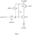
In a possible embodiment of the present disclosure, as shown in FIG. 5, the driving unit 1 may be of various structures, e.g., the driving unit 1 may include a driving thin film transistor (DTFT).
When the driving unit 1 includes the driving transistor DTFT, there may exist various connection modes for the pixel driving circuit. Some of the connection modes will be given, and corresponding operation procedures will be described hereinafter.
In a first connection mode, as shown in FIGS. 2 and 5, a first electrode of the driving transistor DTFT may be connected to the light-emitting unit 10. The first end of the capacitor unit 2 and the data write-in unit 3 may be connected to a gate electrode of the driving transistor DTFT. The power source control unit 4 may be connected to a second electrode of the driving transistor DTFT. The first light-emitting control unit 5 may be connected to the gate electrode of the driving transistor DTFT, and configured to, within the predetermined time period T3 of the light-emitting stage, control the power source signal input end ELVDD to be electrically connected to the gate electrode of the driving transistor DTFT under the control of the second light-emitting control end EM2.
To be specific, as shown in FIG. 6, the operation procedure of the pixel driving circuit in the first connection mode will be described as follows.
At the data write-in stage T1, as shown in FIG. 7a , a data voltage may be applied to the corresponding data line Data, and a gate driving signal may be applied to the corresponding gate line Gate. The data write-in unit 3 may be in an operating state under the control of the gate driving signal, so as to enable the corresponding data line Data to be electrically connected to the gate electrode of the driving transistor DTFT, thereby to write the data voltage into the gate electrode of the driving transistor DTFT and store the data voltage in the capacitor unit 2.
Within the actual light-emitting time period T2 of the light-emitting stage, as shown in FIG. 7b , the power source control unit 4 may be in an operating state under the control of the first light-emitting control end EM1, so as to enable the power source signal input end ELVDD to be electrically connected to the second electrode of the driving transistor DTFT, thereby to transmit a power source signal from the power source signal input end ELVDD to the second electrode of the driving transistor DTFT. At this time, the driving transistor DTFT may be turned on under the control of the data voltage and the power source signal, so as to drive the light-emitting unit 10 to emit light.
Within the predetermined time period T3 of the light-emitting stage, as shown in FIG. 7c , the first light-emitting control unit 5 may control the power source signal input end ELVDD to be electrically connected to the gate electrode of the driving transistor DTFT under the control of the second light-emitting control end EM2, so as to turn off the driving transistor DTFT, thereby to enable the light-emitting unit 10 not to emit light.
In a possible embodiment of the present disclosure, in the first connection mode, the data write-in unit 3, the power source control unit 4 and the first light-emitting control unit 5 may each be of various structures. As shown in FIG. 5, the data write-in unit 3 may include a first switching transistor M1, a gate electrode of which is connected to the corresponding gate line Gate, a first electrode of which is connected to the gate electrode of the driving transistor DTFT, and a second electrode of which is connected to the corresponding data line Data. The power source control unit 4 may include a second switching transistor M2, a gate electrode of which is connected to the first light-emitting control end EM1, a first electrode of which is connected to the second electrode of the driving transistor DTFT, and a second electrode of which is connected to the power source signal input end ELVDD. The first light-emitting control unit 5 may include a third switching transistor M3, a gate electrode of which is connected to the second light-emitting control end EM2, a first electrode of which is connected to the power source signal input end ELVDD, and a second electrode of which is connected to the gate electrode of the driving transistor DTFT.
It should be appreciated that, when the data write-in unit 3 is in the operating state, the first switching transistor M1 may be turned on, and when the data write-in unit 3 is not in the operating state, the first switching transistor M1 may be turned off. When the power source control unit 4 is in the operating state, the first switching transistor M2 may be turned on, and when the power source control unit 4 is not in the operating state, the second switching transistor M2 may be turned off. When the first light-emitting control unit 5 is in the operating state, the third switching transistor M3 may be turned on, and when the first light-emitting control unit 5 is not in the operating state, the third transistor M3 may be turned off.
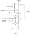
In a second connection mode, as shown in FIGS. 4 and 8, the first electrode of the driving transistor DTFT may be connected to the light-emitting unit 10, the first end of the capacitor unit 2 may be connected to the gate electrode of the driving transistor DTFT, and the data write-in unit 3 and the power source control unit 4 may be connected to the second electrode of the driving transistor DTFT. The first light-emitting control unit 5 may be connected to the gate electrode of the driving transistor DTFT, and configured to, within the predetermined time period T3 of the light-emitting stage, control the power source signal input end ELVDD to be electrically connected to the gate electrode of the driving transistor DTFT under the control of the second light-emitting control end EM2.
In the second connection mode, the pixel driving circuit may further include a first resetting unit 6 and a compensation unit 7. The first resetting unit 6 may be connected to a resetting control end Reset, the gate electrode of the driving transistor DTFT and a reference signal input end Vref, and configured to control the gate electrode of the driving transistor DTFT to be electrically connected to, or electrically disconnected from, the reference signal input end Vref under the control of the resetting control end Reset. The compensation unit 7 may be connected to the corresponding gate line Gate, and the gate electrode and the first electrode of the driving transistor DTFT, and configured to control the gate electrode of the driving transistor DTFT to be electrically connected to, or electrically disconnected from, the first electrode of the driving transistor DTFT under the control of the corresponding gate line Gate.
To be specific, as shown in FIG. 9, an operation procedure of the pixel driving circuit in the second connection mode will be described as follows.
At a resetting stage T0, a reference voltage may be applied to the reference signal input end Vref. The first resetting unit 6 may control the gate electrode of the driving transistor DTFT to be electrically connected to the reference signal input end Vref under the control of the resetting control end Reset, so as to enable a potential at the gate electrode of the driving transistor DTFT to be the reference voltage. The power source control unit 4 may not be in the operating state under the control of the first light-emitting control end EM1, so as to control the power source signal input end ELVDD to be electrically disconnected from the second electrode of the driving transistor DTFT.
At the data write-in stage T1, the driving transistor DTFT may be turned on under the control of the reference voltage. The first resetting unit 6 may control the gate electrode of the driving transistor DTFT to be electrically disconnected from the reference signal input end Vref under the control of the resetting control end Reset. The power source control unit 4 may not be in the operating state under the control of the first light-emitting control end EM1, so it may continuously control the power source signal input end ELVDD to be electrically disconnected from the second electrode of the driving transistor DTFT. A data voltage may be applied to the corresponding data line Data, and a gate driving signal may be applied to the corresponding gate line Gate. The data write-in unit 3 may be in the operating state under the control of the gate driving signal, so as to enable the corresponding data line Data to be electrically connected to the second electrode of the driving transistor DTFT. In addition, the compensation unit 7 may be in an operating state under the control of the gate driving signal, so as to control the gate electrode of the driving transistor DTFT to be electrically connected to, or electrically disconnected from, the first electrode of the driving transistor DTFT, thereby to write the data voltage Vdata into the gate electrode of the driving transistor DTFT through the data write-in unit 3, the driving transistor DTFT and the compensation unit 7 until a voltage applied to the gate electrode of the driving transistor DTFT is equal to Vdata+Vth (where Vth represents a threshold voltage of the driving transistor DTFT), and store Vdata+Vth in the capacitor unit 2.
Within the actual light-emitting time period T2 of the light-emitting stage, the data write-in unit 3 and the compensation unit 7 may each not be in the operating state under the control of the corresponding gate line Gate. The power source control unit 4 may be in the operating state under the control of the first light-emitting control end EM1, so as to control the power source signal input end ELVDD to be electrically connected to the second electrode of the driving transistor DTFT, thereby to apply the power source signal from the power source signal input end ELVDD to the second electrode of the driving transistor DTFT. At this time, the driving transistor DTFT may be turned on under the control of the potential at the gate electrode of the driving transistor DTFT (i.e., Vdata+Vth) and the power source signal, so as to drive the light-emitting unit 10 to emit light.
Within the predetermined time period T3 of the light-emitting stage, the first light-emitting control unit 5 may control the power source signal input end ELVDD to be electrically connected to the gate electrode of the driving transistor DTFT under the control of the second light-emitting control end EM2, so as to turn off the driving transistor DTFT, thereby to enable the light-emitting unit 10 not to emit light.
In a possible embodiment of the present disclosure, as shown in FIGS. 4 and 8 again, the pixel driving circuit may further include a second resetting unit 8 and a second light-emitting control unit 9. The second resetting unit 8 may be connected to the corresponding gate line Gate, the light-emitting unit 10 and the reference signal input end Vref, and configured to control the light-emitting unit 10 to be electrically connected to, or electrically disconnected from, the reference signal input end Vref under the control of the corresponding gate line Gate. The first electrode of the driving transistor DTFT may be connected to the light-emitting unit 10 through the second light-emitting control unit 9. The second light-emitting control unit 9 may be connected to the first light-emitting control end EM1, the first electrode of the driving transistor DTFT and the light-emitting unit 10, and configured to control the first electrode of the driving transistor DTFT to be electrically connected to, or electrically disconnected from, the light-emitting unit 10 under the control of the first light-emitting control end EM1.
To be specific, when the pixel diving circuit further includes the second resetting unit 8 and the second light-emitting control unit 9, the operation procedure of the pixel driving circuit will be described as follows.
At the data write-in state T1, the second resetting unit 8 may control the light-emitting unit 10 to be electrically connected to the reference signal input end Vref under the control of the corresponding gate line Gate, so as to reset the light-emitting unit 10. At the stages other than data write-in stage, the second resetting unit 8 may control the light-emitting unit 10 to be electrically disconnected from the reference signal input end Vref under the control of the corresponding gate line Gate.
At the light-emitting stage (including T2 and T3), the second light-emitting control unit 9 may control the first electrode of the driving transistor DTFT to be electrically connected to the light-emitting unit 10 under the control of the first light-emitting control end EM1. At the resetting stage T0 and the data write-in stage T1, the second light-emitting control unit 9 may control the first electrode of the driving transistor DTFT to be electrically connected to the light-emitting unit 10 under the control of the first light-emitting control end EM1.
It should be appreciated that, the light-emitting unit 10 may be an OLED, an anode of which is connected to the second resetting unit 8.
In a possible embodiment of the present disclosure, as shown in FIG. 8, in the second connection mode, the data write-in unit 3, the power source control unit 4, the first light-emitting control unit 5, the first resetting unit 6, the second resetting unit 8, the compensation unit 7 and the second light-emitting control unit 9 may each be of various structures. For example, the power source control unit 4 may include a second switching transistor M2, a gate electrode of which is connected to the first light-emitting control end EM1, a first electrode of which is connected to the second electrode of the driving transistor DTFT, and a second electrode of which is connected to the power source signal input end ELVDD. The first light-emitting control unit 5 may include a third switching transistor M3, a gate electrode of which is connected to the second light-emitting control end EM2, a first electrode of which is connected to the power source signal input end ELVDD, and a second electrode of which is connected to the gate electrode of the driving transistor DTFT. The first resetting unit 6 may include a fourth switching transistor M4, a gate electrode of which is connected to the resetting control end Reset, a first electrode of which is connected to the gate electrode of the driving transistor DTFT, and a second electrode of which is connected to the reference signal input end Vref. The second resetting unit 8 may include a fifth switching transistor M5, a gate electrode of which is connected to the corresponding gate line Gate, a first electrode of which is connected to the light-emitting unit 10, and a second electrode of which is connected to the reference signal input end Vref. The compensation unit 7 may include a sixth switching transistor M6, a gate electrode of which is connected to the corresponding gate line Gate, a first electrode of which is connected to the gate electrode of the driving transistor DTFT, and a second electrode of which is connected to the first electrode of the driving transistor DTFT. The second light-emitting control unit 9 may include a seventh switching transistor M7, a gate electrode of which is connected to the first light-emitting control end EM1, a first electrode of which is connected to the light-emitting unit 10, and a second electrode of which is connected to the first electrode of the driving transistor DTFT. The data write-in unit 3 may include an eighth switching transistor M8, a gate electrode of which is connected to the corresponding gate line Gate, a first electrode of which is connected to the second electrode of the driving transistor DTFT, and a second electrode of which is connected to the corresponding data line Data. It should be appreciated that, the capacitor unit 2 may include a first capacitor C1.
In a possible embodiment of the present disclosure, the predetermined time period T3 may be a time period between a predetermined time point and an ending time point. The ending time point may be a time point where the light-emitting stage is ended. The predetermined time point may be any time point between T/16+D and T/4+D, where D represents a start time point of the light-emitting stage, and T represents a frame.
To be specific, the light-emitting stage may include the actual light-emitting time period T2 and the predetermined time period T3. Within the light-emitting time period T2, the light-emitting unit 10 may emit light, and within the predetermined time period T3, the light-emitting unit 10 may not emit light. A range of the predetermined time period T3 may be set according to the practical need, as long as it is able for the viewer to clearly view each image and it is able to prevent the occurrence of the ghosts. In a possible embodiment of the present disclosure, the predetermined time period may be any time point Y between T/16+D and T/4+D, and the ending time point may be a time point where the light-emitting stage is ended, i.e., the actual light-emitting time period T2 may be between the start time point of the light-emitting stage and the time point Y, and the predetermined time period T3 may be between the time point Y and the ending time point of the light-emitting stage.
It should be appreciated that, the pixel driving circuit has been described hereinabove merely on the basis of the above-mentioned circuit structure. In some other embodiments of the present disclosure, each unit of the pixel driving circuit may also be of any other structure, which will not be particularly defined herein. In addition, the driving transistor DTFT and the switching transistors may each be a TFT, a field effect transistor (FET) or any other element having a same characteristic. In order to differentiate two electrodes other than a gate electrode from each other, one of the two electrodes is called as first electrode and the other is called as second electrode. In actual use, the first electrode may be a drain electrode while the second electrode may be a source electrode, or the first electrode may be a source electrode while the second electrode may be a drain electrode. In addition, the driving transistor DTFT and the switching transistors may each be an N-type or a P-type transistor according to the practical need.
The present disclosure further provides in some embodiments a method of driving the above-mentioned pixel driving circuit, which includes: at the data write-in stage T1, applying a data voltage to the corresponding data line Data, and applying a gate driving signal to a corresponding gate line Gate, so as to control the data write-in unit 3 to be in an operating state under the control of the gate driving signal and control the corresponding data line Data to be electrically connected to the driving unit 1, thereby to write the data voltage into the driving unit 1 and store the data voltage in the capacitor unit 2; within the actual light-emitting time period T2 of the light-emitting stage, controlling the power source control unit 4 to be in an operating state under the control of the first light-emitting control end EM1, so as to control the power source signal input end ELVDD to be electrically connected to the driving unit 1, transmit a power source signal from the power source signal input end ELVDD to the driving unit 1, and enable the driving unit 1 to be in the operating state under the control of the data voltage and the power source signal, thereby to drive the light-emitting unit 10 to emit light; and within the predetermined time period T3 of the light-emitting stage, controlling, by the first light-emitting control unit 5, the power source signal input end ELVDD to be electrically connected to the driving unit 1 under the control of the second light-emitting control end EM2, thereby to disable the driving unit 1 and enable the light-emitting unit 10 not to emit light.
On the basis of the driving procedure of the pixel driving circuit, the light-emitting unit 10 may emit light after the light-emitting stage begins, and the light-emitting unit 10 may not emit light within the predetermined time period T3 of the light-emitting stage. As a result, it is able to reduce a light-emitting duty ratio of the light-emitting unit 10 and reduce a retention time of each image, thereby to prevent the occurrence of dynamic ghosts.
The present disclosure further provides in some embodiments a display device including N above-mentioned pixel driving circuits, where N is a positive integer.
When the pixel driving circuit drives the light-emitting unit 10 to emit light, it is able to prevent the occurrence of ghosts. Hence, when the display device includes the above-mentioned pixel driving circuit, it is also able to prevent the occurrence of dynamic ghosts when an image is displayed, thereby to improve a display effect of the display device.
In a possible embodiment of the present disclosure, the display device may further include: N pixel units 300 arranged in a matrix form and in X rows (as shown in FIG. 10), the pixel units 300 corresponding to the pixel driving circuits respectively; X gate lines corresponding to the X rows of pixel units 300 respectively; and X light-emitting control lines corresponding to the X rows of pixel units 300 respectively, the first light-emitting control end EM1 being connected to a corresponding light-emitting control line. A second light-emitting control end EM2 may be connected to an Mth gate line randomly selected from an (X/16+C)th gate line to an (X/4+C)th gate line, or connected to an Mth light-emitting control line randomly selected from an (X/16+C)th light-emitting control line to an (X/4+C)th light-emitting control line, where C has a value acquired by subtracting 1 from the number of rows corresponding to the second light-emitting control end EM2. When M is greater than X, the second light-emitting control end EM2 may be connected to an (M−X)th gate line or an (M−X)th light-emitting control line.
To be specific, the display device may include X gate lines, and each gate line may be connected to the data write-in unit 3 of a corresponding pixel driving circuit. The display device may further include X light-emitting control lines, and each light-emitting control line may be connected to the power source control unit 4 of the corresponding pixel driving circuit, i.e., the first light-emitting control end EM1 connected to the power source control unit 4 may be connected to a corresponding light-emitting control line.
In a possible embodiment of the present disclosure, in order to prevent the introduction of any other additional signal line into the display device, the second light-emitting control end EM2 connected to the first light-emitting control unit 5 of the pixel driving circuit may be connected to the corresponding gate line or light-emitting control line of the display device according to the practical need. For example, the second light-emitting control end EM2 may be connected to the Mth gate line randomly selected from the (X/16+C)th gate line to the (X/4+C)th gate line, or connected to an Mth light-emitting control line randomly selected from the (X/16+C)th light-emitting control line to the (X/4+C)th light-emitting control line. In addition, when M is greater than X, the second light-emitting control end EM2 may be connected to the (M−X)th gate line or the (M−X)th light-emitting control line.
More specifically, a connection mode of the second light-emitting control end EM2 may be determined in accordance with a type of the third switching transistor M3 of the first light-emitting control unit 5. For example, when the third switching transistor is an N-type transistor, the second light-emitting control end EM2 may be connected to the corresponding light-emitting control line, so as to control an on state and an off state of the third switching transistor M3 through the corresponding light-emitting control line. When the third switching transistor is a P-type transistor, the second light-emitting control end EM2 may be connected to the corresponding gate line, so as to control the on state and the off state of the third switching transistor M3 through the corresponding gate line.
A connection relationship of the display device will be described hereinafter illustratively. As shown in FIG. 10, EOA represents a light-emitting control signal output unit, an output end of which is connected to a corresponding light-emitting control line connected to the corresponding first light-emitting control end EM1. EOA1 represents a light-emitting control signal output unit corresponding to the pixel units 300 in a first row, EOA481 represents a light-emitting control signal output unit corresponding to the pixel units 300 in a 481st row, EOA961 represents a light-emitting control signal output unit corresponding to the pixel units 300 in a 961st row, and EOA1441 represents a light-emitting control signal output unit corresponding to the pixel units 300 in a 1441st row. The second light-emitting control end EM2 corresponding to the pixel units in the first row may be connected to a 481st light-emitting control line which is connected to EOA481. The second light-emitting control end EM2 corresponding to the pixel units 300 in the 481st row may be connected to a 961st light-emitting control line which is connected to EOA961. The second light-emitting control end EM2 corresponding to the pixel units 300 in the 961st row may be connected to a 1441st light-emitting control line which is connected to EOA1441. The second light-emitting control end EM2 corresponding to the pixel units 300 in the 1441st row may be connected to the first light-emitting control line which is connected to EOA1.
It should be appreciated that, the features, structures or materials may be combined in any embodiment or embodiments in an appropriate manner.
The above embodiments are for illustrative purposes only, but the present disclosure is not limited thereto. Obviously, a person skilled in the art may make further modifications and improvements without departing from the spirit of the present disclosure, and these modifications and improvements shall also fall within the scope of the present disclosure.

Claims (20)

What is claimed is:
1. A pixel driving circuit for driving a light-emitting unit, comprising:
a driving unit connected to the light-emitting unit;
a capacitor unit, one end of the capacitor unit is connected to the driving unit, and a second end of the capacitor unit is connected to a power source signal input end;
a data write-in unit connected to a corresponding gate line in a row direction, a corresponding data line in a column direction and the driving unit;
a power source control unit connected to a first light-emitting control end, the power source signal input end and the driving unit; and
a first light-emitting control unit connected to a second light-emitting control end, the power source signal input end and the driving unit, and configured to, within a predetermined time period of a light-emitting stage, control the power source signal input end to be electrically connected to the driving unit under the control of the second light-emitting control end, stop the operation of the driving unit, and enable the light-emitting unit stop emitting light.
2. The pixel driving circuit according to claim 1, wherein the driving unit comprises a driving transistor, a first electrode of the driving transistor is connected to the light-emitting unit;
the first end of the capacitor unit is connected to a gate electrode of the driving transistor;
the data write-in unit is connected to the gate electrode of the driving transistor;
the power source control unit is connected to a second electrode of the driving transistor; and
the first light-emitting control unit is connected to the gate electrode of the driving transistor, and further configured to, within the predetermined time period of the light-emitting stage, control the power source signal input end to be electrically connected to the gate electrode of the driving transistor under the control of the second light-emitting control end.
3. The pixel driving circuit according to claim 2, wherein the predetermined time period is a time period between a predetermined time point and an ending time point, the ending time point is a time point where the light-emitting stage is ended, and the predetermined time point is any time point between T/16+D and T/4+D, where D represents a start time point of the light-emitting stage, and T represents a frame of time for display.
4. The pixel driving circuit according to claim 2, wherein the data write-in unit comprises a first switching transistor, a gate electrode of which is connected to the corresponding gate line, a first electrode of which is connected to the gate electrode of the driving transistor, and a second electrode of which is connected to the corresponding data line;
the power source control unit comprises a second switching transistor, a gate electrode of which is connected to the first light-emitting control end, a first electrode of which is connected to the second electrode of the driving transistor, and a second electrode of which is connected to the power source signal input end; and
the first light-emitting control unit comprises a third switching transistor, a gate electrode of which is connected to the second light-emitting control end, a first electrode of which is connected to the power source signal input end, and a second electrode of which is connected to the gate electrode of the driving transistor.
5. The pixel driving circuit according to claim 1, wherein the driving unit comprises a driving transistor, a first electrode of the driving transistor is connected to the light-emitting unit;
the first end of the capacitor unit is connected to a gate electrode of the driving unit;
the data write-in unit is connected to a second electrode of the driving transistor;
the power source control unit is connected to a second electrode of the driving transistor; and
the first light-emitting control unit is connected to the gate electrode of the driving transistor, and further configured to, within the predetermined time period of the light-emitting stage, control the power source signal input end to be electrically connected to the gate electrode of the driving transistor under the control of the second light-emitting control end,
wherein the pixel driving circuit further comprises:
a first resetting unit connected to a resetting control end, the gate electrode of the driving transistor and a reference signal input end respectively, and configured to control the gate electrode of the driving transistor to be electrically connected to, or electrically disconnected from, the reference signal input end under the control of the resetting control end; and
a compensation unit connected to the corresponding gate line, the gate electrode of the driving transistor and the first electrode of the driving transistor respectively, and configured to control the gate electrode of the driving transistor to be electrically connected to, or electrically disconnected from, the first electrode of the driving transistor under the control of the corresponding gate line.
6. The pixel driving circuit according to claim 5, further comprising:
a second resetting unit connected to the corresponding gate line, the light-emitting unit and the reference signal input end, and configured to control the light-emitting unit to be electrically connected to, or electrically disconnected from, the reference signal input end under the control of the corresponding, gate line; and
a second light-emitting control unit, a first electrode of the driving transistor being connected to the light-emitting unit via the second light-emitting control unit, the second light-emitting control unit being connected to the first light-emitting control end, the first electrode of the driving transistor and the light-emitting unit, and configured to control the first electrode of the driving transistor to be electrically connected to, or electrically disconnected from, the light-emitting unit under the control of the first light-emitting control end.
7. The pixel driving circuit according to claim 6, wherein the power source control unit comprises a second switching transistor, a gate electrode of which is connected to the first light-emitting control end, a first electrode of which is connected to the second electrode of the driving transistor, and a second electrode of which is connected to the power source signal input end;
the first light-emitting control unit comprises a third switching transistor, a gate electrode of which is connected to the second light-emitting control end, a first electrode of which is connected to the power source signal input end, and a second electrode of which is connected to the gate electrode of the driving transistor;
the first resetting unit comprises a fourth switching transistor, a gate electrode of which is connected to the resetting control end, a first electrode of which is connected to the gate electrode of the driving transistor, and a second electrode of which is connected to the reference signal input end;
the second resetting unit comprises a fifth switching transistor, a gate electrode of which is connected to the corresponding gate line, a first electrode of which is connected to the light-emitting unit, and a second electrode of which is connected to the reference signal input end;
the compensation unit comprises a sixth switching transistor, a gate electrode of which is connected to the corresponding gate line, a first electrode of which is connected to the gate electrode of the driving transistor, and a second electrode of which is connected to the first electrode of the driving transistor;
the second light-emitting control unit comprises a seventh switching transistor, a gate electrode of which is connected to the first light-emitting control end, a first electrode of which is connected to the light-emitting unit, and a second electrode of which is connected to the first electrode of the driving transistor; and
the data write-in unit comprises an eighth switching transistor, a gate electrode of which is connected to the corresponding gate line, a first electrode of which is connected to the second electrode of the driving transistor, and a second electrode of which is connected to the corresponding data line.
8. The pixel driving circuit according to claim 5, wherein the predetermined time period is a time period between a predetermined time point and an ending time point, the ending time point is a time point where the light-emitting stage is ended, and the predetermined time point is any time point between T/16+D and T/4+D, where D represents a start time point of the light-emitting stage, and T represents a frame of time for display.
9. A method of driving the pixel driving circuit according to claim 1, comprising, within the predetermined time period of the light-emitting stage, controlling, by a first light-emitting control unit, a power source signal input end to be electrically connected to a driving unit under the control of a second light-emitting control end, stop the operation of the driving unit, and enable the light-emitting unit stop emitting light.
10. The method according to claim 9, wherein the driving unit comprises a driving transistor, a first electrode of the driving transistor is connected to the light-emitting unit;
the first end of the capacitor unit is connected to a gate electrode of the driving transistor;
the data write-in unit is connected to the gate electrode of the driving transistor;
the power source control unit is connected to a second electrode of the driving transistor; and
the first light-emitting control unit is connected to the gate electrode of the driving transistor, and further configured to, within the predetermined time period of the light-emitting stage, control the power source signal input end to be electrically connected to the gate electrode of the driving transistor under the control of the second light-emitting control end.
11. The method according to claim 9, wherein the driving unit comprises a driving transistor, a first electrode of the driving transistor is connected to the light-emitting unit;
the first end of the capacitor unit is connected to a gate electrode of the driving unit;
the data write-in unit is connected to a second electrode of the driving transistor;
the power source control unit is connected to a second electrode of the driving transistor; and
the first light-emitting control unit is connected to the gate electrode of the driving transistor, and further configured to, within the predetermined time period of the light-emitting stage, control the power source signal input end to be electrically connected to the gate electrode of the driving transistor under the control of the second light-emitting control end,
wherein the pixel driving circuit further comprises:
a first resetting unit connected to a resetting, control end, the gate electrode of the driving transistor and a reference signal input end respectively, and configured to control the gate electrode of the driving transistor to be electrically connected to, or electrically disconnected from, the reference signal input end under the control of the resetting control end; and
a compensation unit connected to the corresponding gate line, the gate electrode of the driving transistor and the first electrode of the driving transistor respectively, and configured to control the gate electrode of the driving transistor to be electrically connected to, or electrically disconnected from, the first electrode of the driving transistor under the control of the corresponding gate line.
12. The method according to claim 11, wherein the pixel driving circuit further comprises:
a second resetting unit connected to the corresponding gate line, the light-emitting unit and the reference signal input end, and configured to control the light-emitting unit to be electrically connected to, or electrically disconnected from, the reference signal input end under the control of the corresponding gate line; and
a second light-emitting control unit, a first electrode of the driving transistor being connected to the light-emitting unit via the second light-emitting control unit, the second light-emitting control unit being connected to the first light-emitting control end, the first electrode of the driving transistor and the light-emitting unit, and configured to control the first electrode of the driving transistor to be electrically connected to, or electrically disconnected from, the light-emitting unit under the control of the first light-emitting control end.
13. A display device, comprising N pixel driving circuits according to claim 1, wherein N is a positive integer.
14. The display device according to claim 13, further comprising:
N pixel units arranged in a matrix form and in X rows, the pixel units corresponding to the pixel driving circuits respectively;
X gate lines corresponding to the X rows of pixel units respectively; and
X light-emitting control lines corresponding to the X rows of pixel units respectively, a first light-emitting control end being connected to a corresponding light-emitting control line,
wherein a second light-emitting control end is connected to an Mth gate line randomly selected from an (X/16+C)th gate line to an (X/4+C)th gate line, or connected to an Mth light-emitting control line randomly selected from an (X/16+C)th light-emitting control line to an (X/4+C)th light-emitting control line, where C has a value acquired by subtracting 1 from the number of rows corresponding to the second light-emitting control end,
wherein when M is greater than X, the second light-emitting control end is connected to an (M−X)th gate line or an (M−X)th light-emitting control line.
15. The display device according to claim 13, wherein the driving unit comprises a driving transistor, a first electrode of the driving transistor is connected to the light-emitting unit;
the first end of the capacitor unit is connected to a gate electrode of the driving transistor;
the data write-in unit is connected to the gate electrode of the driving transistor;
the power source control unit is connected to a second electrode of the driving transistor; and
the first light-emitting, control unit is connected to the gate electrode of the driving transistor, and further configured to, within the predetermined time period of the light-emitting stage, control the power source signal input end to be electrically connected to the gate electrode of the driving transistor under the control of the second light-emitting control end.
16. The display device according to claim 15, wherein the predetermined time period is a time period between a predetermined time point and an ending time point, the ending time point is a time point where the light-emitting stage is ended, and the predetermined time point is any time point between T/16+D and T/4+D, where D represents a start time point of the light-emitting stage, and T represents a frame of time for display.
17. The display device according to claim 15, wherein the data write-in unit comprises a first switching transistor, a gate electrode of which is connected to the corresponding gate line, a first electrode of which is connected to the gate electrode of the driving transistor, and a second electrode of which is connected to the corresponding data line;
the power source control unit comprises a second switching transistor, a gate electrode of which is connected to the first light-emitting control end, a first electrode of which is connected to the second electrode of the driving transistor, and a second electrode of which is connected to the power source signal input end; and
the first light-emitting control unit comprises a third switching transistor, a gate electrode of which is connected to the second light-emitting control end, a first electrode of which is connected to the power source signal input end, and a second electrode of which is connected to the gate electrode of the driving transistor.
18. The display device according to claim 13, wherein the driving unit comprises a driving transistor, a first electrode of the driving transistor is connected to the light-emitting unit;
the first end of the capacitor unit is connected to a gate electrode of the driving unit;
the data write-in unit is connected to a second electrode of the driving transistor;
the power source control unit is connected to a second electrode of the driving transistor; and
the first light-emitting control unit is connected to the gate electrode of the driving transistor, and further configured to, within the predetermined time period of the light-emitting stage, control the power source signal input end to be electrically connected to the gate electrode of the driving transistor under the control of the second light-emitting control end,
wherein the pixel driving circuit further comprises:
a first resetting unit connected to a resetting control end, the gate electrode of the driving transistor and a reference signal input end respectively, and configured to control the gate electrode of the driving transistor to be electrically connected to, or electrically disconnected from, the reference signal input end under the control of the resetting control end; and
a compensation unit connected to the corresponding gate line, the gate electrode of the driving transistor and the first electrode of the driving transistor respectively, and configured to control the gate electrode of the driving transistor to be electrically connected to, or electrically disconnected from, the first electrode of the driving transistor under the control of the corresponding gate line.
19. The display device according to claim 18, further comprising:
a second resetting unit connected to the corresponding gate line, the light-emitting unit and the reference signal input end, and configured to control the light-emitting unit to be electrically connected to, or electrically disconnected from, the reference signal input end under the control of the corresponding gate line; and
a second light-emitting control unit, a first electrode of the driving transistor being connected to the light-emitting unit via the second light-emitting control unit, the second light-emitting control unit being connected to the first light-emitting control end, the first electrode of the driving transistor and the light-emitting unit, and configured to control the first electrode of the driving transistor to be electrically connected to, or electrically disconnected from, the light-emitting unit under the control of the first light-emitting control end.
20. The display device according to claim 18, wherein the power source control unit comprises a second switching transistor, a gate electrode of which is connected to the first light-emitting control end, a first electrode of which is connected to the second electrode of the driving transistor, and a second electrode of which is connected to the power source signal input end;
the first light-emitting control unit comprises a third switching transistor, a gate electrode of which is connected to the second light-emitting control end, a first electrode of which is connected to the power source signal input end, and a second electrode of which is connected to the gate electrode of the driving transistor;
the first resetting unit comprises a fourth switching transistor, a gate electrode of which is connected to the resetting control end, a first electrode of which is connected to the gate electrode of the driving transistor, and a second electrode of which is connected to the reference signal input end;
the second resetting unit comprises a fifth switching transistor, a gate electrode of which is connected to the corresponding gate line, a first electrode of which is connected to the light-emitting unit, and a second electrode of which is connected to the reference signal input end;
the compensation unit comprises a sixth switching transistor, a gate electrode of which is connected to the corresponding gate line, a first electrode of which is connected to the gate electrode of the driving transistor, and a second electrode of which is connected to the first electrode of the driving transistor;
the second light-emitting control unit comprises a seventh switching transistor, a gate electrode of which is connected to the first light-emitting control end, a first electrode of which is connected to the light-emitting unit, and a second electrode of Which is connected to the first electrode of the driving transistor; and
the data write-in unit comprises an eighth switching transistor, a gate electrode of which is connected to the corresponding gate line, a first electrode of which is connected to the second electrode of the driving transistor, and a second electrode of which is connected to the corresponding data line.
US16/616,234 2018-04-28 2019-04-18 Pixel driving circuit, driving method thereof and display device Active US10971069B2 (en)

Applications Claiming Priority (3)

Application Number Priority Date Filing Date Title
CN201810401414.3 2018-04-28
CN201810401414.3A CN108288456B (en) 2018-04-28 2018-04-28 A pixel driving circuit, a driving method thereof, and a display device
PCT/CN2019/083223 WO2019206018A1 (en) 2018-04-28 2019-04-18 Pixel drive circuit and drive method thereof, and display device

Publications (2)

Publication Number Publication Date
US20200090591A1 US20200090591A1 (en) 2020-03-19
US10971069B2 true US10971069B2 (en) 2021-04-06

Family

ID=62834662

Family Applications (1)

Application Number Title Priority Date Filing Date
US16/616,234 Active US10971069B2 (en) 2018-04-28 2019-04-18 Pixel driving circuit, driving method thereof and display device

Country Status (3)

Country Link
US (1) US10971069B2 (en)
CN (1) CN108288456B (en)
WO (1) WO2019206018A1 (en)

Cited By (1)

* Cited by examiner, † Cited by third party
Publication number Priority date Publication date Assignee Title
US12020640B2 (en) 2020-10-21 2024-06-25 Lg Display Co., Ltd. Pixel and organic light emitting display device comprising the same

Families Citing this family (14)

* Cited by examiner, † Cited by third party
Publication number Priority date Publication date Assignee Title
CN108288456B (en) * 2018-04-28 2021-03-19 京东方科技集团股份有限公司 A pixel driving circuit, a driving method thereof, and a display device
WO2020061886A1 (en) * 2018-09-27 2020-04-02 深圳市柔宇科技有限公司 Pixel circuit and display panel
CN111312168B (en) * 2018-12-11 2022-10-04 成都辰显光电有限公司 Pixel circuit, display device and driving method of pixel circuit
CN111312162B (en) * 2018-12-11 2023-03-31 成都辰显光电有限公司 Pixel circuit, display device and driving method of pixel circuit
US11315480B2 (en) 2019-01-25 2022-04-26 Boe Technology Group Co., Ltd. Pixel driving circuit, driving method thereof, and display panel
CN110517631B (en) * 2019-08-30 2021-05-18 成都辰显光电有限公司 Pixel driving circuit, display panel and driving method of pixel driving circuit
CN110619851A (en) * 2019-09-24 2019-12-27 京东方科技集团股份有限公司 Pixel circuit, driving method and display device
CN111179851A (en) * 2020-02-25 2020-05-19 合肥鑫晟光电科技有限公司 Pixel circuit and driving method thereof, and display device
CN111445861A (en) * 2020-05-06 2020-07-24 合肥京东方卓印科技有限公司 Pixel drive circuit and drive method, shift register circuit, and display device
CN112017609B (en) * 2020-09-03 2021-07-23 Tcl华星光电技术有限公司 Control method of display panel, display panel and display device
CN112037714A (en) * 2020-09-14 2020-12-04 京东方科技集团股份有限公司 A pixel circuit, a driving method thereof, a display panel and a display device
CN114863885A (en) * 2022-06-21 2022-08-05 义乌清越光电技术研究院有限公司 Pixel circuit, array substrate and display device
CN115101004B (en) * 2022-06-30 2024-09-24 厦门天马微电子有限公司 Pixel driving circuit, driving method thereof, light-emitting panel and display device
CN115440167B (en) * 2022-08-30 2023-11-07 惠科股份有限公司 Pixel circuit, display panel and display device

Citations (19)

* Cited by examiner, † Cited by third party
Publication number Priority date Publication date Assignee Title
WO2001020591A1 (en) 1999-09-11 2001-03-22 Koninklijke Philips Electronics N.V. Active matrix electroluminescent display device
CN1685390A (en) 2002-09-23 2005-10-19 皇家飞利浦电子股份有限公司 Matrix display device with photosensitive element
US20050237001A1 (en) 2004-04-27 2005-10-27 Tohoku Pioneer Corporation Light emitting display device and drive control method thereof
CN1835057A (en) 2005-03-18 2006-09-20 精工爱普生株式会社 Organic electroluminescent device, driving method thereof and electronic apparatus
US20080068312A1 (en) 2006-09-18 2008-03-20 Samsung Sdi Co., Ltd. Organic light emitting display apparatus and method of driving the same
US20110025586A1 (en) 2009-08-03 2011-02-03 Lee Baek-Woon Organic light emitting display and driving method thereof
US20110090208A1 (en) * 2009-10-21 2011-04-21 Boe Technology Group Co., Ltd. Voltage-driving pixel unit, driving method and oled display
CN104021762A (en) 2014-05-30 2014-09-03 京东方科技集团股份有限公司 Pixel circuit, driving method thereof, and display device
CN104658483A (en) 2015-03-16 2015-05-27 深圳市华星光电技术有限公司 AMOLED (Active Matrix Organic Light Emitting Display) pixel driving circuit and method
US20170124958A1 (en) 2015-10-28 2017-05-04 Samsung Display Co., Ltd. Display device
CN106652912A (en) 2016-12-13 2017-05-10 上海天马有机发光显示技术有限公司 Organic light emitting pixel driving circuit, driving method and organic light emitting display panel
US20170263188A1 (en) * 2016-03-09 2017-09-14 Samsung Display Co., Ltd. Scan driver and display apparatus having the same
US20180068611A1 (en) * 2015-07-24 2018-03-08 Ignis Innovation Inc. Pixels and reference circuits and timing techniques
US10008153B2 (en) * 2015-08-13 2018-06-26 Boe Technology Group Co., Ltd. Pixel circuit and driving method thereof, array substrate, display device
CN108288456A (en) 2018-04-28 2018-07-17 京东方科技集团股份有限公司 A kind of pixel-driving circuit and its driving method, display device
US20180218677A1 (en) * 2015-10-22 2018-08-02 Boe Technology Group Co., Ltd. Pixel driving circuit, display apparatus and driving method thereof
US20190073955A1 (en) * 2017-09-06 2019-03-07 Boe Technology Group Co., Ltd. Pixel driving circuit and driving method thereof, display device
US20190096322A1 (en) * 2017-09-28 2019-03-28 Boe Technology Group Co., Ltd. Pixel driving circuit and method thereof, and display device
US20200312244A1 (en) * 2018-05-09 2020-10-01 Boe Technology Group Co., Ltd. Pixel circuit and drive method thereof, display substrate, display device

Family Cites Families (2)

* Cited by examiner, † Cited by third party
Publication number Priority date Publication date Assignee Title
JP6257225B2 (en) * 2013-08-30 2018-01-10 キヤノン株式会社 Display control device, display control device control method, and program
CN105161053B (en) * 2015-09-11 2017-08-11 深圳市明微电子股份有限公司 A kind of anti-smear row sweeps control chip and anti-smear LED display circuit

Patent Citations (27)

* Cited by examiner, † Cited by third party
Publication number Priority date Publication date Assignee Title
WO2001020591A1 (en) 1999-09-11 2001-03-22 Koninklijke Philips Electronics N.V. Active matrix electroluminescent display device
CN1685390A (en) 2002-09-23 2005-10-19 皇家飞利浦电子股份有限公司 Matrix display device with photosensitive element
US20060038751A1 (en) 2002-09-23 2006-02-23 Koninkijkle Phillips Electroncis N.V. Matrix display device with photosensitive element
US20050237001A1 (en) 2004-04-27 2005-10-27 Tohoku Pioneer Corporation Light emitting display device and drive control method thereof
CN1691111A (en) 2004-04-27 2005-11-02 东北先锋电子股份有限公司 Light emitting display device and drive control method thereof
CN1835057A (en) 2005-03-18 2006-09-20 精工爱普生株式会社 Organic electroluminescent device, driving method thereof and electronic apparatus
US20060208974A1 (en) 2005-03-18 2006-09-21 Seiko Epson Corporation Organic electroluminescent device, driving method thereof and electronic apparatus
US20080068312A1 (en) 2006-09-18 2008-03-20 Samsung Sdi Co., Ltd. Organic light emitting display apparatus and method of driving the same
US20110025586A1 (en) 2009-08-03 2011-02-03 Lee Baek-Woon Organic light emitting display and driving method thereof
CN101989404A (en) 2009-08-03 2011-03-23 三星移动显示器株式会社 Organic light emitting display and driving method thereof
US20110090208A1 (en) * 2009-10-21 2011-04-21 Boe Technology Group Co., Ltd. Voltage-driving pixel unit, driving method and oled display
CN104021762A (en) 2014-05-30 2014-09-03 京东方科技集团股份有限公司 Pixel circuit, driving method thereof, and display device
CN104658483A (en) 2015-03-16 2015-05-27 深圳市华星光电技术有限公司 AMOLED (Active Matrix Organic Light Emitting Display) pixel driving circuit and method
US20160307502A1 (en) 2015-03-16 2016-10-20 Shenzhen China Star Optoelectronics Technology Co. Ltd. Amoled pixel driving circuit and pixel driving method
US20180068611A1 (en) * 2015-07-24 2018-03-08 Ignis Innovation Inc. Pixels and reference circuits and timing techniques
US10008153B2 (en) * 2015-08-13 2018-06-26 Boe Technology Group Co., Ltd. Pixel circuit and driving method thereof, array substrate, display device
US20180218677A1 (en) * 2015-10-22 2018-08-02 Boe Technology Group Co., Ltd. Pixel driving circuit, display apparatus and driving method thereof
CN106652905A (en) 2015-10-28 2017-05-10 三星显示有限公司 Display device
US20170124958A1 (en) 2015-10-28 2017-05-04 Samsung Display Co., Ltd. Display device
US20170263188A1 (en) * 2016-03-09 2017-09-14 Samsung Display Co., Ltd. Scan driver and display apparatus having the same
US20170221420A1 (en) 2016-12-13 2017-08-03 Shanghai Tianma AM-OLED Co., Ltd. Organic light-emitting pixel driving circuit, driving method, and organic light-emitting display panel
CN106652912A (en) 2016-12-13 2017-05-10 上海天马有机发光显示技术有限公司 Organic light emitting pixel driving circuit, driving method and organic light emitting display panel
US20190073955A1 (en) * 2017-09-06 2019-03-07 Boe Technology Group Co., Ltd. Pixel driving circuit and driving method thereof, display device
US20190096322A1 (en) * 2017-09-28 2019-03-28 Boe Technology Group Co., Ltd. Pixel driving circuit and method thereof, and display device
CN108288456A (en) 2018-04-28 2018-07-17 京东方科技集团股份有限公司 A kind of pixel-driving circuit and its driving method, display device
US20200090591A1 (en) 2018-04-28 2020-03-19 Boe Technology Group Co., Ltd. Pixel driving circuit, driving method thereof and display device
US20200312244A1 (en) * 2018-05-09 2020-10-01 Boe Technology Group Co., Ltd. Pixel circuit and drive method thereof, display substrate, display device

Non-Patent Citations (15)

* Cited by examiner, † Cited by third party
Title
1st Chinese Office Action, English Translation.
2nd Chinese Office Action, English Translation.
CN101989404A, English Abstract and U.S. Equivalent U.S. Pub. No. 2011/0025586.
CN104021762A, English Abstract and Machine Translation.
CN104658483A, English Abstract and U.S. Equivalent U.S. Pub. No. 2016/0307502.
CN106652905A, English Abstract and U.S. Equivalent U.S. Pub. No. 2017/0124958.
CN106652912A, English Abstract and U.S. Equivalent U.S. Pub. No. 2017/0221420.
CN108288456A, English Abstract and U.S. Equivalent U.S. Pub. No. 2020/0090591.
CN1685390A, English Abstract and U.S. Equivalent U.S. Pub. No. 2006/0038751.
CN1691111A, English Abstract and U.S. Equivalent U.S. Pub. No. 2005/0237001.
CN1835057A, English Abstract and U.S. Equivalent U.S. Pub. No. 2006/0208974.
First Office Action for Chinese Application No. 201810401414.3, dated Jun. 4, 2019, 5 Pages.
International Search Report and Written Opinion for Application No. PCT/CN2019/083223, dated Jul. 24, 2019, 11 Pages.
International Search Report and Written Opinion, English Translation.
Second Office Action for Chinese Application No. 201810401414.3, dated Dec. 4, 2019, 8 Pages.

Cited By (2)

* Cited by examiner, † Cited by third party
Publication number Priority date Publication date Assignee Title
US12020640B2 (en) 2020-10-21 2024-06-25 Lg Display Co., Ltd. Pixel and organic light emitting display device comprising the same
US12437718B2 (en) 2020-10-21 2025-10-07 Lg Display Co., Ltd. Pixel and organic light emitting display device comprising the same

Also Published As

Publication number Publication date
WO2019206018A1 (en) 2019-10-31
CN108288456A (en) 2018-07-17
US20200090591A1 (en) 2020-03-19
CN108288456B (en) 2021-03-19

Similar Documents

Publication Publication Date Title
US10971069B2 (en) Pixel driving circuit, driving method thereof and display device
US20220139321A1 (en) Pixel circuit and method of driving the same, display device
US10916199B2 (en) Display panel and driving method of pixel circuit
US10650751B2 (en) Pixel driving circuit and driving method thereof, display device
US10551903B2 (en) Organic light emitting display apparatus
US9747839B2 (en) Pixel driving circuit, driving method, array substrate and display apparatus
US10403201B2 (en) Pixel driving circuit, pixel driving method, display panel and display device
US10290260B2 (en) Pixel circuit having third drive circuit connected to first drive circuit and second drive circuit respectively, display panel and driving method
US9084331B2 (en) Active matrix organic light emitting diode circuit and operating method of the same
US11132951B2 (en) Pixel circuit, pixel driving method and display device
US11127342B2 (en) Pixel circuit for driving light emitting diode to emit light and method of controlling the pixel circuit
US9852687B2 (en) Display device and driving method
US9286830B2 (en) Display apparatus
CN112908246A (en) Pixel circuit, driving method thereof and display panel
CN103946912B (en) Display device and control method thereof
US10937368B2 (en) Voltage compensation method, voltage compensation device, display device and computer-readable storage medium
CN112908245B (en) Pixel circuit, driving method thereof and display panel
JP2015102793A (en) Display device and method for driving display device
WO2020155902A1 (en) Pixel driving circuit, pixel driving method and display apparatus
CN104599641A (en) OLED pixel unit and driving method thereof, as well as OLED display device
JP2019082548A (en) Pixel circuit, display device, driving method of pixel circuit, and electronic apparatus
US9990887B2 (en) Pixel driving circuit, method for driving the same, shift register, display panel and display device
CN110675826A (en) Display panel, driving method thereof and display device
US10997912B2 (en) Method of driving display panel, driving circuit, and display unit
WO2019080256A1 (en) Oled pixel driving circuit and driving method thereof

Legal Events

Date Code Title Description
FEPP Fee payment procedure

Free format text: ENTITY STATUS SET TO UNDISCOUNTED (ORIGINAL EVENT CODE: BIG.); ENTITY STATUS OF PATENT OWNER: LARGE ENTITY

AS Assignment

Owner name: BOE TECHNOLOGY GROUP CO., LTD., CHINA

Free format text: ASSIGNMENT OF ASSIGNORS INTEREST;ASSIGNORS:WANG, TIESHI;PENG, KUANJUN;QIN, WEI;AND OTHERS;SIGNING DATES FROM 20190909 TO 20191118;REEL/FRAME:051098/0154

STPP Information on status: patent application and granting procedure in general

Free format text: NOTICE OF ALLOWANCE MAILED -- APPLICATION RECEIVED IN OFFICE OF PUBLICATIONS

STPP Information on status: patent application and granting procedure in general

Free format text: PUBLICATIONS -- ISSUE FEE PAYMENT RECEIVED

STPP Information on status: patent application and granting procedure in general

Free format text: PUBLICATIONS -- ISSUE FEE PAYMENT VERIFIED

STCF Information on status: patent grant

Free format text: PATENTED CASE

MAFP Maintenance fee payment

Free format text: PAYMENT OF MAINTENANCE FEE, 4TH YEAR, LARGE ENTITY (ORIGINAL EVENT CODE: M1551); ENTITY STATUS OF PATENT OWNER: LARGE ENTITY

Year of fee payment: 4