US10968208B2 - Compound for organic electronic element, organic electronic element comprising the same, and electronic device thereof - Google Patents
Compound for organic electronic element, organic electronic element comprising the same, and electronic device thereof Download PDFInfo
- Publication number
- US10968208B2 US10968208B2 US15/758,827 US201615758827A US10968208B2 US 10968208 B2 US10968208 B2 US 10968208B2 US 201615758827 A US201615758827 A US 201615758827A US 10968208 B2 US10968208 B2 US 10968208B2
- Authority
- US
- United States
- Prior art keywords
- group
- mmol
- core
- organic
- compound
- Prior art date
- Legal status (The legal status is an assumption and is not a legal conclusion. Google has not performed a legal analysis and makes no representation as to the accuracy of the status listed.)
- Active, expires
Links
- 150000001875 compounds Chemical class 0.000 title claims abstract description 73
- 239000011368 organic material Substances 0.000 claims abstract description 37
- 238000000034 method Methods 0.000 claims description 53
- 239000000463 material Substances 0.000 claims description 48
- 125000003118 aryl group Chemical group 0.000 claims description 29
- 125000000623 heterocyclic group Chemical group 0.000 claims description 29
- 125000005842 heteroatom Chemical group 0.000 claims description 27
- 229910052760 oxygen Inorganic materials 0.000 claims description 23
- 229910052757 nitrogen Inorganic materials 0.000 claims description 21
- 229910052717 sulfur Inorganic materials 0.000 claims description 21
- 229910052698 phosphorus Inorganic materials 0.000 claims description 20
- 229910052710 silicon Inorganic materials 0.000 claims description 20
- 125000003983 fluorenyl group Chemical group C1(=CC=CC=2C3=CC=CC=C3CC12)* 0.000 claims description 16
- 125000000217 alkyl group Chemical group 0.000 claims description 15
- YZCKVEUIGOORGS-OUBTZVSYSA-N Deuterium Chemical compound [2H] YZCKVEUIGOORGS-OUBTZVSYSA-N 0.000 claims description 11
- 229910052805 deuterium Inorganic materials 0.000 claims description 11
- 125000001424 substituent group Chemical group 0.000 claims description 11
- 125000003545 alkoxy group Chemical group 0.000 claims description 10
- 229910052736 halogen Inorganic materials 0.000 claims description 10
- 150000002367 halogens Chemical class 0.000 claims description 10
- 125000006749 (C6-C60) aryl group Chemical group 0.000 claims description 9
- 125000005567 fluorenylene group Chemical group 0.000 claims description 9
- 125000003358 C2-C20 alkenyl group Chemical group 0.000 claims description 8
- 229910052739 hydrogen Inorganic materials 0.000 claims description 8
- 239000001257 hydrogen Substances 0.000 claims description 8
- 125000004104 aryloxy group Chemical group 0.000 claims description 7
- 125000006761 (C6-C60) arylene group Chemical group 0.000 claims description 6
- 125000006736 (C6-C20) aryl group Chemical group 0.000 claims description 5
- 150000002431 hydrogen Chemical class 0.000 claims description 5
- 125000003837 (C1-C20) alkyl group Chemical group 0.000 claims description 3
- 125000006649 (C2-C20) alkynyl group Chemical group 0.000 claims description 3
- ZOXJGFHDIHLPTG-UHFFFAOYSA-N Boron Chemical group [B] ZOXJGFHDIHLPTG-UHFFFAOYSA-N 0.000 claims description 3
- BLRPTPMANUNPDV-UHFFFAOYSA-N Silane Chemical group [SiH4] BLRPTPMANUNPDV-UHFFFAOYSA-N 0.000 claims description 3
- GNPVGFCGXDBREM-UHFFFAOYSA-N germanium atom Chemical group [Ge] GNPVGFCGXDBREM-UHFFFAOYSA-N 0.000 claims description 3
- 125000000449 nitro group Chemical group [O-][N+](*)=O 0.000 claims description 3
- 230000008569 process Effects 0.000 claims description 3
- 229910052705 radium Inorganic materials 0.000 claims description 3
- 229910052701 rubidium Inorganic materials 0.000 claims description 3
- 239000011248 coating agent Substances 0.000 claims description 2
- 238000000576 coating method Methods 0.000 claims description 2
- 239000004020 conductor Substances 0.000 claims description 2
- 125000004093 cyano group Chemical group *C#N 0.000 claims description 2
- 238000003618 dip coating Methods 0.000 claims description 2
- 238000005286 illumination Methods 0.000 claims description 2
- 238000007641 inkjet printing Methods 0.000 claims description 2
- 238000007639 printing Methods 0.000 claims description 2
- 125000005373 siloxane group Chemical group [SiH2](O*)* 0.000 claims description 2
- 238000004528 spin coating Methods 0.000 claims description 2
- 239000010410 layer Substances 0.000 description 116
- 230000015572 biosynthetic process Effects 0.000 description 105
- 238000003786 synthesis reaction Methods 0.000 description 105
- 239000000047 product Substances 0.000 description 49
- BWHMMNNQKKPAPP-UHFFFAOYSA-L potassium carbonate Chemical compound [K+].[K+].[O-]C([O-])=O BWHMMNNQKKPAPP-UHFFFAOYSA-L 0.000 description 36
- 229910001868 water Inorganic materials 0.000 description 33
- JGFZNNIVVJXRND-UHFFFAOYSA-N N,N-Diisopropylethylamine (DIPEA) Chemical compound CCN(C(C)C)C(C)C JGFZNNIVVJXRND-UHFFFAOYSA-N 0.000 description 30
- YXFVVABEGXRONW-UHFFFAOYSA-N Toluene Chemical compound CC1=CC=CC=C1 YXFVVABEGXRONW-UHFFFAOYSA-N 0.000 description 30
- XLYOFNOQVPJJNP-UHFFFAOYSA-N water Chemical compound O XLYOFNOQVPJJNP-UHFFFAOYSA-N 0.000 description 23
- CTQNGGLPUBDAKN-UHFFFAOYSA-N O-Xylene Chemical group CC1=CC=CC=C1C CTQNGGLPUBDAKN-UHFFFAOYSA-N 0.000 description 20
- 238000002347 injection Methods 0.000 description 20
- 239000007924 injection Substances 0.000 description 20
- XHXFXVLFKHQFAL-UHFFFAOYSA-N phosphoryl trichloride Chemical compound ClP(Cl)(Cl)=O XHXFXVLFKHQFAL-UHFFFAOYSA-N 0.000 description 20
- LPNYRYFBWFDTMA-UHFFFAOYSA-N potassium tert-butoxide Chemical compound [K+].CC(C)(C)[O-] LPNYRYFBWFDTMA-UHFFFAOYSA-N 0.000 description 20
- RIOQSEWOXXDEQQ-UHFFFAOYSA-N triphenylphosphine Chemical compound C1=CC=CC=C1P(C=1C=CC=CC=1)C1=CC=CC=C1 RIOQSEWOXXDEQQ-UHFFFAOYSA-N 0.000 description 20
- NFHFRUOZVGFOOS-UHFFFAOYSA-N Pd(PPh3)4 Substances [Pd].C1=CC=CC=C1P(C=1C=CC=CC=1)C1=CC=CC=C1.C1=CC=CC=C1P(C=1C=CC=CC=1)C1=CC=CC=C1.C1=CC=CC=C1P(C=1C=CC=CC=1)C1=CC=CC=C1.C1=CC=CC=C1P(C=1C=CC=CC=1)C1=CC=CC=C1 NFHFRUOZVGFOOS-UHFFFAOYSA-N 0.000 description 18
- 229910000027 potassium carbonate Inorganic materials 0.000 description 18
- 230000000052 comparative effect Effects 0.000 description 16
- 0 *c(c(*)c1*)c(*)c(*)c1-c1c(cccc2)c2sc(-c2nc(c([s]c3ccccc33)c3c3ccccc33)c3c3c2cccc3)n1 Chemical compound *c(c(*)c1*)c(*)c(*)c1-c1c(cccc2)c2sc(-c2nc(c([s]c3ccccc33)c3c3ccccc33)c3c3c2cccc3)n1 0.000 description 14
- 230000005525 hole transport Effects 0.000 description 13
- KZPYGQFFRCFCPP-UHFFFAOYSA-N 1,1'-bis(diphenylphosphino)ferrocene Chemical compound [Fe+2].C1=CC=C[C-]1P(C=1C=CC=CC=1)C1=CC=CC=C1.C1=CC=C[C-]1P(C=1C=CC=CC=1)C1=CC=CC=C1 KZPYGQFFRCFCPP-UHFFFAOYSA-N 0.000 description 10
- CSNNHWWHGAXBCP-UHFFFAOYSA-L Magnesium sulfate Chemical compound [Mg+2].[O-][S+2]([O-])([O-])[O-] CSNNHWWHGAXBCP-UHFFFAOYSA-L 0.000 description 10
- 229910019213 POCl3 Inorganic materials 0.000 description 10
- 229910002666 PdCl2 Inorganic materials 0.000 description 10
- IPWKHHSGDUIRAH-UHFFFAOYSA-N bis(pinacolato)diboron Chemical compound O1C(C)(C)C(C)(C)OB1B1OC(C)(C)C(C)(C)O1 IPWKHHSGDUIRAH-UHFFFAOYSA-N 0.000 description 10
- 229940078552 o-xylene Drugs 0.000 description 10
- PIBWKRNGBLPSSY-UHFFFAOYSA-L palladium(II) chloride Chemical compound Cl[Pd]Cl PIBWKRNGBLPSSY-UHFFFAOYSA-L 0.000 description 10
- SCVFZCLFOSHCOH-UHFFFAOYSA-M potassium acetate Chemical compound [K+].CC([O-])=O SCVFZCLFOSHCOH-UHFFFAOYSA-M 0.000 description 10
- XEKOWRVHYACXOJ-UHFFFAOYSA-N Ethyl acetate Chemical compound CCOC(C)=O XEKOWRVHYACXOJ-UHFFFAOYSA-N 0.000 description 9
- SMWDFEZZVXVKRB-UHFFFAOYSA-N Quinoline Chemical compound N1=CC=CC2=CC=CC=C21 SMWDFEZZVXVKRB-UHFFFAOYSA-N 0.000 description 9
- 239000007795 chemical reaction product Substances 0.000 description 9
- ZUOUZKKEUPVFJK-UHFFFAOYSA-N diphenyl Chemical compound C1=CC=CC=C1C1=CC=CC=C1 ZUOUZKKEUPVFJK-UHFFFAOYSA-N 0.000 description 9
- 239000000203 mixture Substances 0.000 description 9
- NHNAEZDWNCRWRW-UHFFFAOYSA-N 2-bromobenzamide Chemical compound NC(=O)C1=CC=CC=C1Br NHNAEZDWNCRWRW-UHFFFAOYSA-N 0.000 description 8
- 125000004432 carbon atom Chemical group C* 0.000 description 8
- IYYZUPMFVPLQIF-UHFFFAOYSA-N dibenzothiophene Chemical compound C1=CC=C2C3=CC=CC=C3SC2=C1 IYYZUPMFVPLQIF-UHFFFAOYSA-N 0.000 description 8
- 238000000434 field desorption mass spectrometry Methods 0.000 description 8
- 239000002019 doping agent Substances 0.000 description 7
- 125000001997 phenyl group Chemical group [H]C1=C([H])C([H])=C(*)C([H])=C1[H] 0.000 description 7
- 125000003367 polycyclic group Chemical group 0.000 description 7
- UFWIBTONFRDIAS-UHFFFAOYSA-N Naphthalene Chemical compound C1=CC=CC2=CC=CC=C21 UFWIBTONFRDIAS-UHFFFAOYSA-N 0.000 description 6
- 238000000429 assembly Methods 0.000 description 6
- 230000000712 assembly Effects 0.000 description 6
- 238000006243 chemical reaction Methods 0.000 description 6
- YNPNZTXNASCQKK-UHFFFAOYSA-N phenanthrene Chemical compound C1=CC=C2C3=CC=CC=C3C=CC2=C1 YNPNZTXNASCQKK-UHFFFAOYSA-N 0.000 description 6
- VYPSYNLAJGMNEJ-UHFFFAOYSA-N Silicium dioxide Chemical compound O=[Si]=O VYPSYNLAJGMNEJ-UHFFFAOYSA-N 0.000 description 5
- 125000000732 arylene group Chemical group 0.000 description 5
- 235000010290 biphenyl Nutrition 0.000 description 5
- 230000000875 corresponding effect Effects 0.000 description 5
- 125000000524 functional group Chemical group 0.000 description 5
- 229910052943 magnesium sulfate Inorganic materials 0.000 description 5
- 239000012044 organic layer Substances 0.000 description 5
- 150000003413 spiro compounds Chemical class 0.000 description 5
- 239000000758 substrate Substances 0.000 description 5
- UJOBWOGCFQCDNV-UHFFFAOYSA-N 9H-carbazole Chemical compound C1=CC=C2C3=CC=CC=C3NC2=C1 UJOBWOGCFQCDNV-UHFFFAOYSA-N 0.000 description 4
- OKTJSMMVPCPJKN-UHFFFAOYSA-N Carbon Chemical group [C] OKTJSMMVPCPJKN-UHFFFAOYSA-N 0.000 description 4
- JUJWROOIHBZHMG-UHFFFAOYSA-N Pyridine Chemical compound C1=CC=NC=C1 JUJWROOIHBZHMG-UHFFFAOYSA-N 0.000 description 4
- CZPWVGJYEJSRLH-UHFFFAOYSA-N Pyrimidine Chemical compound C1=CN=CN=C1 CZPWVGJYEJSRLH-UHFFFAOYSA-N 0.000 description 4
- 125000001931 aliphatic group Chemical group 0.000 description 4
- 239000004305 biphenyl Substances 0.000 description 4
- 230000000903 blocking effect Effects 0.000 description 4
- 229910052799 carbon Inorganic materials 0.000 description 4
- 239000012141 concentrate Substances 0.000 description 4
- 125000000753 cycloalkyl group Chemical group 0.000 description 4
- 238000000151 deposition Methods 0.000 description 4
- RDOWQLZANAYVLL-UHFFFAOYSA-N phenanthridine Chemical compound C1=CC=C2C3=CC=CC=C3C=NC2=C1 RDOWQLZANAYVLL-UHFFFAOYSA-N 0.000 description 4
- 239000000741 silica gel Substances 0.000 description 4
- 229910002027 silica gel Inorganic materials 0.000 description 4
- 125000004429 atom Chemical group 0.000 description 3
- 230000008901 benefit Effects 0.000 description 3
- 125000004122 cyclic group Chemical group 0.000 description 3
- 238000005401 electroluminescence Methods 0.000 description 3
- 125000002950 monocyclic group Chemical group 0.000 description 3
- 125000006574 non-aromatic ring group Chemical group 0.000 description 3
- 239000001301 oxygen Substances 0.000 description 3
- -1 oxygen radical Chemical class 0.000 description 3
- 238000006467 substitution reaction Methods 0.000 description 3
- 125000006757 (C2-C30) heterocyclic group Chemical group 0.000 description 2
- JYEUMXHLPRZUAT-UHFFFAOYSA-N 1,2,3-triazine Chemical compound C1=CN=NN=C1 JYEUMXHLPRZUAT-UHFFFAOYSA-N 0.000 description 2
- YJTKZCDBKVTVBY-UHFFFAOYSA-N 1,3-Diphenylbenzene Chemical group C1=CC=CC=C1C1=CC=CC(C=2C=CC=CC=2)=C1 YJTKZCDBKVTVBY-UHFFFAOYSA-N 0.000 description 2
- MYKQKWIPLZEVOW-UHFFFAOYSA-N 11h-benzo[a]carbazole Chemical compound C1=CC2=CC=CC=C2C2=C1C1=CC=CC=C1N2 MYKQKWIPLZEVOW-UHFFFAOYSA-N 0.000 description 2
- PEZWWBDREVNGLQ-UHFFFAOYSA-N 2-(3-chlorophenyl)-3-phenylquinoxaline Chemical compound ClC1=CC=CC(C=2C(=NC3=CC=CC=C3N=2)C=2C=CC=CC=2)=C1 PEZWWBDREVNGLQ-UHFFFAOYSA-N 0.000 description 2
- RUVUDYBTZRIRHH-UHFFFAOYSA-N 6-[(4-bromophenyl)methyl]indolo[3,2-b]quinoxaline Chemical compound C1=CC(Br)=CC=C1CN1C2=NC3=CC=CC=C3N=C2C2=CC=CC=C21 RUVUDYBTZRIRHH-UHFFFAOYSA-N 0.000 description 2
- NJBMMMJOXRZENQ-UHFFFAOYSA-N 6H-pyrrolo[2,3-f]quinoline Chemical compound c1cc2ccc3[nH]cccc3c2n1 NJBMMMJOXRZENQ-UHFFFAOYSA-N 0.000 description 2
- MMSSNAOTILFWIO-UHFFFAOYSA-N C1=CC2=C(C=C1)C1=C(O2)C2=C(C3=C(C=CC=C3)C(C3=CC=C(N4C5=C(C=CC=C5)C5=C4C=CC=C5)C=C3)=N2)C2=C1C=CC=C2.C1=CC2=C3C(=C1)C=CC1=C3C(=CC(C3=NC4=C(C5=C3C=CC=C5)C3=C(C=CC=C3)C3=C4OC4=C3C=CC=C4)=C1)/C=C\2.C1=CC2=NC(C3=NC4=C(C5=C3C=CC=C5)C3=C(C=CC=C3)C3=C4OC4=C3C=CC=C4)=C3C=CC=CC3=C2C=C1 Chemical compound C1=CC2=C(C=C1)C1=C(O2)C2=C(C3=C(C=CC=C3)C(C3=CC=C(N4C5=C(C=CC=C5)C5=C4C=CC=C5)C=C3)=N2)C2=C1C=CC=C2.C1=CC2=C3C(=C1)C=CC1=C3C(=CC(C3=NC4=C(C5=C3C=CC=C5)C3=C(C=CC=C3)C3=C4OC4=C3C=CC=C4)=C1)/C=C\2.C1=CC2=NC(C3=NC4=C(C5=C3C=CC=C5)C3=C(C=CC=C3)C3=C4OC4=C3C=CC=C4)=C3C=CC=CC3=C2C=C1 MMSSNAOTILFWIO-UHFFFAOYSA-N 0.000 description 2
- OZVBMIRHHMCIRI-UHFFFAOYSA-N C1=CC2=CC=C(C3=C4C(=NC(C5=NC6=C(C7=C5C=CC=C7)C5=C(C=CC=C5)C5=C6SC6=C5C=CC=C6)=N3)SC3=C4C=CC=C3)C=C2C=C1.C1=CC2=CC=CC(C3=C4OC5=C(C=CC=C5)C4=NC(C4=NC5=C(C6=C4C=CC=C6)C4=C(C=CC=C4)C4=C5SC5=C4C=CC=C5)=N3)=C2C=C1.C1=CC=C(N(C2=CC=C(C3=NC4=C(C5=C3C=CC=C5)C3=C(C=CC=C3)C3=C4SC4=C3C=CC=C4)C=C2)C2=CC=C3C=CC=CC3=C2)C=C1 Chemical compound C1=CC2=CC=C(C3=C4C(=NC(C5=NC6=C(C7=C5C=CC=C7)C5=C(C=CC=C5)C5=C6SC6=C5C=CC=C6)=N3)SC3=C4C=CC=C3)C=C2C=C1.C1=CC2=CC=CC(C3=C4OC5=C(C=CC=C5)C4=NC(C4=NC5=C(C6=C4C=CC=C6)C4=C(C=CC=C4)C4=C5SC5=C4C=CC=C5)=N3)=C2C=C1.C1=CC=C(N(C2=CC=C(C3=NC4=C(C5=C3C=CC=C5)C3=C(C=CC=C3)C3=C4SC4=C3C=CC=C4)C=C2)C2=CC=C3C=CC=CC3=C2)C=C1 OZVBMIRHHMCIRI-UHFFFAOYSA-N 0.000 description 2
- PIBVLKMSJPPSOX-UHFFFAOYSA-N C1=CC2=CC=C(C3=C4C=CC=CC4=NC(C4=NC5=C(C6=C4C=CC=C6)C4=C(C=CC=C4)C4=C5SC5=C4C=CC=C5)=N3)C=C2C=C1.C1=CC=C(C2=C3C=CC4=C(C=CC=C4)C3=NC(C3=NC4=C(C5=C3C=CC=C5)C3=C(C=CC=C3)C3=C4SC4=C3C=CC=C4)=N2)C=C1.C1=CC=C(N(C2=CC=CC=C2)C2=CC=C(C3=C4C=CC=CC4=NC(C4=NC5=C(C6=C4C=CC=C6)C4=C(C=CC=C4)C4=C5SC5=C4C=CC=C5)=N3)C=C2)C=C1 Chemical compound C1=CC2=CC=C(C3=C4C=CC=CC4=NC(C4=NC5=C(C6=C4C=CC=C6)C4=C(C=CC=C4)C4=C5SC5=C4C=CC=C5)=N3)C=C2C=C1.C1=CC=C(C2=C3C=CC4=C(C=CC=C4)C3=NC(C3=NC4=C(C5=C3C=CC=C5)C3=C(C=CC=C3)C3=C4SC4=C3C=CC=C4)=N2)C=C1.C1=CC=C(N(C2=CC=CC=C2)C2=CC=C(C3=C4C=CC=CC4=NC(C4=NC5=C(C6=C4C=CC=C6)C4=C(C=CC=C4)C4=C5SC5=C4C=CC=C5)=N3)C=C2)C=C1 PIBVLKMSJPPSOX-UHFFFAOYSA-N 0.000 description 2
- UITFSEXTNDFDLL-UHFFFAOYSA-N C1=CC2=NC(C3=NC4=C(C5=C3C=CC=C5)C3=C(C=CC=C3)C3=C4SC4=C3C=CC=C4)=NC(C3=CC4=C(C=C3)SC3=C4C=CC=C3)=C2C=C1.C1=CC=C(C2=CC(C3=C4C=CC=CC4=NC(C4=NC5=C(C6=C4C=CC=C6)C4=C(C=CC=C4)C4=C5SC5=C4C=CC=C5)=N3)=CC=C2)C=C1.CC1=CC=C(C2=C3C=CC=CC3=NC(C3=NC4=C(C5=C3C=CC=C5)C3=C(C=CC=C3)C3=C4SC4=C3C=CC=C4)=N2)C=C1 Chemical compound C1=CC2=NC(C3=NC4=C(C5=C3C=CC=C5)C3=C(C=CC=C3)C3=C4SC4=C3C=CC=C4)=NC(C3=CC4=C(C=C3)SC3=C4C=CC=C3)=C2C=C1.C1=CC=C(C2=CC(C3=C4C=CC=CC4=NC(C4=NC5=C(C6=C4C=CC=C6)C4=C(C=CC=C4)C4=C5SC5=C4C=CC=C5)=N3)=CC=C2)C=C1.CC1=CC=C(C2=C3C=CC=CC3=NC(C3=NC4=C(C5=C3C=CC=C5)C3=C(C=CC=C3)C3=C4SC4=C3C=CC=C4)=N2)C=C1 UITFSEXTNDFDLL-UHFFFAOYSA-N 0.000 description 2
- NBZIOQGGIMGCKY-UHFFFAOYSA-N C1=CC2=NC(C3=NC4=C(C=CC5=C4SC4=C5C=CC=C4)C4=C3C=CC=C4)=NC(C3=CC=CC4=C3SC3=C4C=CC=C3)=C2C=C1.C1=CC=C(C2=C3C=CC=CC3=NC(C3=NC4=C(C=CC5=C4SC4=C5C=CC=C4)C4=C3C=CC=C4)=N2)C=C1.C1=CC=C(C2=CC=C(C3=C4C=CC=CC4=NC(C4=NC5=C(C=CC6=C5SC5=C6C=CC=C5)C5=C4C=CC=C5)=N3)C3=C2C=CC=C3)C=C1 Chemical compound C1=CC2=NC(C3=NC4=C(C=CC5=C4SC4=C5C=CC=C4)C4=C3C=CC=C4)=NC(C3=CC=CC4=C3SC3=C4C=CC=C3)=C2C=C1.C1=CC=C(C2=C3C=CC=CC3=NC(C3=NC4=C(C=CC5=C4SC4=C5C=CC=C4)C4=C3C=CC=C4)=N2)C=C1.C1=CC=C(C2=CC=C(C3=C4C=CC=CC4=NC(C4=NC5=C(C=CC6=C5SC5=C6C=CC=C5)C5=C4C=CC=C5)=N3)C3=C2C=CC=C3)C=C1 NBZIOQGGIMGCKY-UHFFFAOYSA-N 0.000 description 2
- XLQBTQYQLVNLNA-UHFFFAOYSA-N C1=CC=C(C2=C3C(=NC(C4=NC5=C(C6=C4C=CC=C6)C4=C(C=C5)OC5=CC=CC=C54)=N2)OC2=C3C=CC=C2)C=C1.C1=CC=C(C2=C3C=CC=CC3=NC(N3C4=C(C=CC=C4)C4=C3C=CC(C3=NC5=C(C6=C3C=CC=C6)C3=C(C=C5)OC5=CC=CC=C53)=C4)=N2)C=C1.C1=CC=C(C2=CC=C(N(C3=CC=C(C4=NC5=C(C6=C4C=CC=C6)C4=C(C=C5)OC5=CC=CC=C54)C=C3)C3=CC=C4C(=C3)C(C3=CC=CC=C3)(C3=CC=CC=C3)C3=C4C=CC=C3)C=C2)C=C1 Chemical compound C1=CC=C(C2=C3C(=NC(C4=NC5=C(C6=C4C=CC=C6)C4=C(C=C5)OC5=CC=CC=C54)=N2)OC2=C3C=CC=C2)C=C1.C1=CC=C(C2=C3C=CC=CC3=NC(N3C4=C(C=CC=C4)C4=C3C=CC(C3=NC5=C(C6=C3C=CC=C6)C3=C(C=C5)OC5=CC=CC=C53)=C4)=N2)C=C1.C1=CC=C(C2=CC=C(N(C3=CC=C(C4=NC5=C(C6=C4C=CC=C6)C4=C(C=C5)OC5=CC=CC=C54)C=C3)C3=CC=C4C(=C3)C(C3=CC=CC=C3)(C3=CC=CC=C3)C3=C4C=CC=C3)C=C2)C=C1 XLQBTQYQLVNLNA-UHFFFAOYSA-N 0.000 description 2
- ZSRCCPYNMLWYKN-UHFFFAOYSA-N C1=CC=C(C2=C3C(=NC(C4=NC5=C(C6=C4C=CC=C6)C4=C(OC6=CC=CC=C64)C4=C5C=CC=C4)=N2)OC2=C3C=CC=C2)C=C1.C1=CC=C(C2=C3C=CC=CC3=NC(N3C4=C(C=CC=C4)C4=C3C=CC(C3=NC5=C(C6=C3C=CC=C6)C3=C(OC6=CC=CC=C63)C3=C5C=CC=C3)=C4)=N2)C=C1.CC1(C)C2=CC(N(C3=CC=C(C4=CC=CC=C4)C=C3)C3=CC=C(C4=NC5=C(C6=C4C=CC=C6)C4=C(OC6=CC=CC=C64)C4=C5C=CC=C4)C=C3)=CC=C2C2=C1C=CC=C2 Chemical compound C1=CC=C(C2=C3C(=NC(C4=NC5=C(C6=C4C=CC=C6)C4=C(OC6=CC=CC=C64)C4=C5C=CC=C4)=N2)OC2=C3C=CC=C2)C=C1.C1=CC=C(C2=C3C=CC=CC3=NC(N3C4=C(C=CC=C4)C4=C3C=CC(C3=NC5=C(C6=C3C=CC=C6)C3=C(OC6=CC=CC=C63)C3=C5C=CC=C3)=C4)=N2)C=C1.CC1(C)C2=CC(N(C3=CC=C(C4=CC=CC=C4)C=C3)C3=CC=C(C4=NC5=C(C6=C4C=CC=C6)C4=C(OC6=CC=CC=C64)C4=C5C=CC=C4)C=C3)=CC=C2C2=C1C=CC=C2 ZSRCCPYNMLWYKN-UHFFFAOYSA-N 0.000 description 2
- PBVNVEYYWQIKMZ-UHFFFAOYSA-N C1=CC=C(C2=C3C(=NC(C4=NC5=C(C=CC6=C5SC5=C6C=CC=C5)C5=C4C=CC=C5)=N2)SC2=C3C=CC=C2)C=C1.C1=CC=C(C2=C3C=CC4=C(C=CC=C4)C3=NC(C3=NC4=C(C=CC5=C4SC4=C5C=CC=C4)C4=C3C=CC=C4)=N2)C=C1.C1=CC=C(C2=NC3=C(C=C(C4=NC5=C(C=CC6=C5OC5=C6C=CC=C5)C5=C4C=CC=C5)C=C3)C3=C2C=CC=C3)C=C1 Chemical compound C1=CC=C(C2=C3C(=NC(C4=NC5=C(C=CC6=C5SC5=C6C=CC=C5)C5=C4C=CC=C5)=N2)SC2=C3C=CC=C2)C=C1.C1=CC=C(C2=C3C=CC4=C(C=CC=C4)C3=NC(C3=NC4=C(C=CC5=C4SC4=C5C=CC=C4)C4=C3C=CC=C4)=N2)C=C1.C1=CC=C(C2=NC3=C(C=C(C4=NC5=C(C=CC6=C5OC5=C6C=CC=C5)C5=C4C=CC=C5)C=C3)C3=C2C=CC=C3)C=C1 PBVNVEYYWQIKMZ-UHFFFAOYSA-N 0.000 description 2
- FBYAJCKIKMQMNT-UHFFFAOYSA-N C1=CC=C(C2=C3C=CC4=C(C=CC=C4)C3=NC(C3=NC4=C(C5=C3C=CC=C5)C3=C(C=C4)SC4=CC=CC=C43)=N2)C=C1.C1=CC=C(C2=C3SC4=C(C=CC=C4)C3=NC(C3=NC4=C(C5=C3C=CC=C5)C3=C(C=C4)SC4=CC=CC=C43)=N2)C=C1.C1=CC=C(N(C2=CC=CC=C2)C2=CC=C(C3=C4C=CC=CC4=NC(C4=NC5=C(C6=C4C=CC=C6)C4=C(C=C5)SC5=CC=CC=C54)=N3)C=C2)C=C1 Chemical compound C1=CC=C(C2=C3C=CC4=C(C=CC=C4)C3=NC(C3=NC4=C(C5=C3C=CC=C5)C3=C(C=C4)SC4=CC=CC=C43)=N2)C=C1.C1=CC=C(C2=C3SC4=C(C=CC=C4)C3=NC(C3=NC4=C(C5=C3C=CC=C5)C3=C(C=C4)SC4=CC=CC=C43)=N2)C=C1.C1=CC=C(N(C2=CC=CC=C2)C2=CC=C(C3=C4C=CC=CC4=NC(C4=NC5=C(C6=C4C=CC=C6)C4=C(C=C5)SC5=CC=CC=C54)=N3)C=C2)C=C1 FBYAJCKIKMQMNT-UHFFFAOYSA-N 0.000 description 2
- HRRLATORIRVTIU-UHFFFAOYSA-N C1=CC=C(C2=C3C=CC4=C(C=CC=C4)C3=NC(C3=NC4=C(C5=C3C=CC=C5)C3=C(SC5=CC=CC=C53)C3=C4C=CC=C3)=N2)C=C1.C1=CC=C(N(C2=CC=CC=C2)C2=CC=C(C3=C4C=CC=CC4=NC(C4=NC5=C(C6=C4C=CC=C6)C4=C(SC6=CC=CC=C64)C4=C5C=CC=C4)=N3)C=C2)C=C1.C1=CC=C2C(=C1)SC1=C2C2=C(N=C(C3=NC(C4=CC=C5C=CC=CC5=C4)=C4C(=N3)SC3=C4C=CC=C3)C3=C2C=CC=C3)C2=C1C=CC=C2 Chemical compound C1=CC=C(C2=C3C=CC4=C(C=CC=C4)C3=NC(C3=NC4=C(C5=C3C=CC=C5)C3=C(SC5=CC=CC=C53)C3=C4C=CC=C3)=N2)C=C1.C1=CC=C(N(C2=CC=CC=C2)C2=CC=C(C3=C4C=CC=CC4=NC(C4=NC5=C(C6=C4C=CC=C6)C4=C(SC6=CC=CC=C64)C4=C5C=CC=C4)=N3)C=C2)C=C1.C1=CC=C2C(=C1)SC1=C2C2=C(N=C(C3=NC(C4=CC=C5C=CC=CC5=C4)=C4C(=N3)SC3=C4C=CC=C3)C3=C2C=CC=C3)C2=C1C=CC=C2 HRRLATORIRVTIU-UHFFFAOYSA-N 0.000 description 2
- LJVFTQXTWYUSCV-UHFFFAOYSA-N C1=CC=C(C2=C3C=CC=CC3=NC(C3=NC4=C(C5=C3C=CC=C5)C3=C(C=C4)SC4=CC=CC=C43)=N2)C=C1.C1=CC=C2C(=C1)SC1=C2C2=C(C=C1)N=C(C1=CN=C(C3=CN=CC=C3)N=C1C1=CN=CC=C1)C1=C2C=CC=C1.C1=CC=C2C(=C1)SC1=C2C2=C(C=C1)N=C(C1=NC(C3=CC4=C(C=C3)SC3=C4C=CC=C3)=C3C=CC=CC3=N1)C1=C2C=CC=C1 Chemical compound C1=CC=C(C2=C3C=CC=CC3=NC(C3=NC4=C(C5=C3C=CC=C5)C3=C(C=C4)SC4=CC=CC=C43)=N2)C=C1.C1=CC=C2C(=C1)SC1=C2C2=C(C=C1)N=C(C1=CN=C(C3=CN=CC=C3)N=C1C1=CN=CC=C1)C1=C2C=CC=C1.C1=CC=C2C(=C1)SC1=C2C2=C(C=C1)N=C(C1=NC(C3=CC4=C(C=C3)SC3=C4C=CC=C3)=C3C=CC=CC3=N1)C1=C2C=CC=C1 LJVFTQXTWYUSCV-UHFFFAOYSA-N 0.000 description 2
- VVYLBJOLGXRTJT-UHFFFAOYSA-N C1=CC=C(C2=C3C=CC=CC3=NC(C3=NC4=C(C5=C3C=CC=C5)C3=C(SC5=CC=CC=C53)C3=C4C=CC=C3)=N2)C=C1.C1=CC=C(C2=NC=C(C3=NC4=C(C5=C3C=CC=C5)C3=C(SC5=CC=CC=C53)C3=C4C=CC=C3)C(C3=CC=CC=C3)=N2)C=C1.C1=CC=C2C(=C1)SC1=C2C2=C(N=C(C3=NC(C4=CC5=C(C=C4)SC4=C5C=CC=C4)=C4C=CC=CC4=N3)C3=C2C=CC=C3)C2=C1C=CC=C2 Chemical compound C1=CC=C(C2=C3C=CC=CC3=NC(C3=NC4=C(C5=C3C=CC=C5)C3=C(SC5=CC=CC=C53)C3=C4C=CC=C3)=N2)C=C1.C1=CC=C(C2=NC=C(C3=NC4=C(C5=C3C=CC=C5)C3=C(SC5=CC=CC=C53)C3=C4C=CC=C3)C(C3=CC=CC=C3)=N2)C=C1.C1=CC=C2C(=C1)SC1=C2C2=C(N=C(C3=NC(C4=CC5=C(C=C4)SC4=C5C=CC=C4)=C4C=CC=CC4=N3)C3=C2C=CC=C3)C2=C1C=CC=C2 VVYLBJOLGXRTJT-UHFFFAOYSA-N 0.000 description 2
- NBGHHFROQZHZGV-UHFFFAOYSA-N C1=CC=C(C2=C3C=CC=CC3=NC(N3C4=C(C=C(C5=NC6=C(C7=C5C=CC=C7)C5=C(C=C6)OC6=CC=CC=C65)C=C4)C4=C3N=CC=C4)=N2)C=C1.C1=CC=C(C2=C3C=CC=CC3=NC(N3C4=C(C=CC=C4)C4=C3C3=C(C=CC=C3)C(C3=NC5=C(C6=C3C=CC=C6)C3=C(C=C5)OC5=CC=CC=C53)=C4)=N2)C=C1 Chemical compound C1=CC=C(C2=C3C=CC=CC3=NC(N3C4=C(C=C(C5=NC6=C(C7=C5C=CC=C7)C5=C(C=C6)OC6=CC=CC=C65)C=C4)C4=C3N=CC=C4)=N2)C=C1.C1=CC=C(C2=C3C=CC=CC3=NC(N3C4=C(C=CC=C4)C4=C3C3=C(C=CC=C3)C(C3=NC5=C(C6=C3C=CC=C6)C3=C(C=C5)OC5=CC=CC=C53)=C4)=N2)C=C1 NBGHHFROQZHZGV-UHFFFAOYSA-N 0.000 description 2
- DYNKIFFQSDUYPQ-UHFFFAOYSA-N C1=CC=C(C2=C3C=CC=CC3=NC(N3C4=C(C=C(C5=NC6=C(C7=C5C=CC=C7)C5=C(C=CC=C5)C5=C6C6=CC=CC=C6S5)C=C4)C4=C3N=CC=C4)=N2)C=C1.C1=CC=C(C2=C3C=CC=CC3=NC(N3C4=C(C=CC(C5=NC6=C(C7=C5C=CC=C7)C5=C(C=CC=C5)C5=C6C6=CC=CC=C6S5)=C4)C4=C3C=CC=N4)=N2)C=C1.C1=CC=C2C(=C1)OC1=C2C2=C(C3=C(C=CC=C3)C(C3=CC4=C5C(=C3)C=CC3=C5C(=CC=C3)/C=C\4)=N2)C2=C1C=CC=C2 Chemical compound C1=CC=C(C2=C3C=CC=CC3=NC(N3C4=C(C=C(C5=NC6=C(C7=C5C=CC=C7)C5=C(C=CC=C5)C5=C6C6=CC=CC=C6S5)C=C4)C4=C3N=CC=C4)=N2)C=C1.C1=CC=C(C2=C3C=CC=CC3=NC(N3C4=C(C=CC(C5=NC6=C(C7=C5C=CC=C7)C5=C(C=CC=C5)C5=C6C6=CC=CC=C6S5)=C4)C4=C3C=CC=N4)=N2)C=C1.C1=CC=C2C(=C1)OC1=C2C2=C(C3=C(C=CC=C3)C(C3=CC4=C5C(=C3)C=CC3=C5C(=CC=C3)/C=C\4)=N2)C2=C1C=CC=C2 DYNKIFFQSDUYPQ-UHFFFAOYSA-N 0.000 description 2
- LYHCREIMUXXBGT-UHFFFAOYSA-N C1=CC=C(C2=C3C=CC=CC3=NC(N3C4=C(C=C(C5=NC6=C(C=CC7=C6C6=CC=CC=C6S7)C6=C5C=CC=C6)C=C4)C4=C3C=NC=C4)=N2)C=C1.C1=CC=C(C2=C3C=CC=CC3=NC(N3C4=C(C=NC=C4)C4=C3C=CC(C3=NC5=C(C=CC6=C5C5=CC=CC=C5S6)C5=C3C=CC=C5)=C4)=N2)C=C1.C1=CC=C2C(=C1)OC1=C2C2=C(C=C1)C1=C(C=CC=C1)C(C1=CC(C3=CC=CC4=C3C=CC=C4)=CC=C1)=N2 Chemical compound C1=CC=C(C2=C3C=CC=CC3=NC(N3C4=C(C=C(C5=NC6=C(C=CC7=C6C6=CC=CC=C6S7)C6=C5C=CC=C6)C=C4)C4=C3C=NC=C4)=N2)C=C1.C1=CC=C(C2=C3C=CC=CC3=NC(N3C4=C(C=NC=C4)C4=C3C=CC(C3=NC5=C(C=CC6=C5C5=CC=CC=C5S6)C5=C3C=CC=C5)=C4)=N2)C=C1.C1=CC=C2C(=C1)OC1=C2C2=C(C=C1)C1=C(C=CC=C1)C(C1=CC(C3=CC=CC4=C3C=CC=C4)=CC=C1)=N2 LYHCREIMUXXBGT-UHFFFAOYSA-N 0.000 description 2
- UAAZOJVDUPTOMZ-UHFFFAOYSA-N C1=CC=C(C2=C3C=CC=CC3=NC(N3C4=C(C=C(C5=NC6=CC7=C(C=C6C6=C5C=CC=C6)OC5=CC=CC=C57)C=C4)C4=C3N=CC=C4)=N2)C=C1.C1=CC=C(C2=C3C=CC=CC3=NC(N3C4=C(C=CC=C4)C4=C3C3=C(C=CC=C3)C(C3=NC5=CC6=C(C=C5C5=C3C=CC=C5)OC3=CC=CC=C36)=C4)=N2)C=C1 Chemical compound C1=CC=C(C2=C3C=CC=CC3=NC(N3C4=C(C=C(C5=NC6=CC7=C(C=C6C6=C5C=CC=C6)OC5=CC=CC=C57)C=C4)C4=C3N=CC=C4)=N2)C=C1.C1=CC=C(C2=C3C=CC=CC3=NC(N3C4=C(C=CC=C4)C4=C3C3=C(C=CC=C3)C(C3=NC5=CC6=C(C=C5C5=C3C=CC=C5)OC3=CC=CC=C36)=C4)=N2)C=C1 UAAZOJVDUPTOMZ-UHFFFAOYSA-N 0.000 description 2
- MVWJHMGQKIJNMJ-UHFFFAOYSA-N C1=CC=C(C2=C3C=CC=CC3=NC(N3C4=C(C=CC(C5=NC6=C(C7=C5C=CC=C7)C5=C(C=CC=C5)C5=C6SC6=C5C=CC=C6)=C4)C4=C3C=CC=N4)=N2)C=C1.C1=CC=C(C2=C3C=CC=CC3=NC(N3C4=C(C=CC(C5=NC6=C(C7=C5C=CC=C7)C5=C(C=CC=C5)C5=C6SC6=C5C=CC=C6)=C4)C4=C3N=CC=C4)=N2)C=C1.C1=CC=C(C2=C3C=CC=CC3=NC(N3C4=C(C=CC=C4)C4=C3C=CC(C3=NC5=C(C6=C3C=CC=C6)C3=C(C=CC=C3)C3=C5SC5=C3C=CC=C5)=C4)=N2)C=C1 Chemical compound C1=CC=C(C2=C3C=CC=CC3=NC(N3C4=C(C=CC(C5=NC6=C(C7=C5C=CC=C7)C5=C(C=CC=C5)C5=C6SC6=C5C=CC=C6)=C4)C4=C3C=CC=N4)=N2)C=C1.C1=CC=C(C2=C3C=CC=CC3=NC(N3C4=C(C=CC(C5=NC6=C(C7=C5C=CC=C7)C5=C(C=CC=C5)C5=C6SC6=C5C=CC=C6)=C4)C4=C3N=CC=C4)=N2)C=C1.C1=CC=C(C2=C3C=CC=CC3=NC(N3C4=C(C=CC=C4)C4=C3C=CC(C3=NC5=C(C6=C3C=CC=C6)C3=C(C=CC=C3)C3=C5SC5=C3C=CC=C5)=C4)=N2)C=C1 MVWJHMGQKIJNMJ-UHFFFAOYSA-N 0.000 description 2
- MLFQQHASFOSGDI-UHFFFAOYSA-N C1=CC=C(C2=C3C=CC=CC3=NC(N3C4=C(C=CC=C4)C4=C3C=C(C3=NC5=C(C6=C3C=CC=C6)C3=C(C=C5)C5=CC=CC=C5S3)C=C4)=N2)C=C1.C1=CC=C(C2=C3C=CC=CC3=NC(N3C4=C(C=CN=C4)C4=C3C=C(C3=NC5=C(C6=C3C=CC=C6)C3=C(C=C5)C5=CC=CC=C5S3)C=C4)=N2)C=C1.C1=CC=C(C2=C3C=CC=CC3=NC(N3C4=C(C=NC=C4)C4=C3C=C(C3=NC5=C(C6=C3C=CC=C6)C3=C(C=C5)C5=CC=CC=C5S3)C=C4)=N2)C=C1 Chemical compound C1=CC=C(C2=C3C=CC=CC3=NC(N3C4=C(C=CC=C4)C4=C3C=C(C3=NC5=C(C6=C3C=CC=C6)C3=C(C=C5)C5=CC=CC=C5S3)C=C4)=N2)C=C1.C1=CC=C(C2=C3C=CC=CC3=NC(N3C4=C(C=CN=C4)C4=C3C=C(C3=NC5=C(C6=C3C=CC=C6)C3=C(C=C5)C5=CC=CC=C5S3)C=C4)=N2)C=C1.C1=CC=C(C2=C3C=CC=CC3=NC(N3C4=C(C=NC=C4)C4=C3C=C(C3=NC5=C(C6=C3C=CC=C6)C3=C(C=C5)C5=CC=CC=C5S3)C=C4)=N2)C=C1 MLFQQHASFOSGDI-UHFFFAOYSA-N 0.000 description 2
- XREOUDSVVUAXLI-UHFFFAOYSA-N C1=CC=C(C2=C3C=CC=CC3=NC(N3C4=C(C=CC=C4)C4=C3C=CC(C3=NC5=C(C6=C3C=CC=C6)C3=C(C=CC=C3)C3=C5C5=CC=CC=C5S3)=C4)=N2)C=C1.C1=CC=C(N(C2=CC=C(C3=NC4=C(C5=C3C=CC=C5)C3=C(C=CC=C3)C3=C4C4=CC=CC=C4S3)C=C2)C2=CC=C3C=CC=CC3=C2)C=C1.C1=CC=C2C(=C1)SC1=C2C2=C(C3=C(C=CC=C3)C(C3=NC(C4=C5C=CC=CC5=CC=C4)=C4OC5=C(C=CC=C5)C4=N3)=N2)C2=C1C=CC=C2 Chemical compound C1=CC=C(C2=C3C=CC=CC3=NC(N3C4=C(C=CC=C4)C4=C3C=CC(C3=NC5=C(C6=C3C=CC=C6)C3=C(C=CC=C3)C3=C5C5=CC=CC=C5S3)=C4)=N2)C=C1.C1=CC=C(N(C2=CC=C(C3=NC4=C(C5=C3C=CC=C5)C3=C(C=CC=C3)C3=C4C4=CC=CC=C4S3)C=C2)C2=CC=C3C=CC=CC3=C2)C=C1.C1=CC=C2C(=C1)SC1=C2C2=C(C3=C(C=CC=C3)C(C3=NC(C4=C5C=CC=CC5=CC=C4)=C4OC5=C(C=CC=C5)C4=N3)=N2)C2=C1C=CC=C2 XREOUDSVVUAXLI-UHFFFAOYSA-N 0.000 description 2
- RTUWRPGQVLJIDQ-UHFFFAOYSA-N C1=CC=C(C2=C3C=CC=CC3=NC(N3C4=C(C=CC=C4)C4=C3C=CC(C3=NC5=C(C=CC6=C5C5=CC=CC=C5S6)C5=C3C=CC=C5)=C4)=N2)C=C1.C1=CC=C(C2=C3OC4=C(C=CC=C4)C3=NC(C3=NC4=C(C=CC5=C4C4=CC=CC=C4S5)C4=C3C=CC=C4)=N2)C=C1.CC1(C)C2=CC(N(C3=CC=CC=C3)C3=CC=C(C4=NC5=C(C=CC6=C5C5=CC=CC=C5S6)C5=C4C=CC=C5)C=C3)=CC=C2C2=C1C=CC=C2 Chemical compound C1=CC=C(C2=C3C=CC=CC3=NC(N3C4=C(C=CC=C4)C4=C3C=CC(C3=NC5=C(C=CC6=C5C5=CC=CC=C5S6)C5=C3C=CC=C5)=C4)=N2)C=C1.C1=CC=C(C2=C3OC4=C(C=CC=C4)C3=NC(C3=NC4=C(C=CC5=C4C4=CC=CC=C4S5)C4=C3C=CC=C4)=N2)C=C1.CC1(C)C2=CC(N(C3=CC=CC=C3)C3=CC=C(C4=NC5=C(C=CC6=C5C5=CC=CC=C5S6)C5=C4C=CC=C5)C=C3)=CC=C2C2=C1C=CC=C2 RTUWRPGQVLJIDQ-UHFFFAOYSA-N 0.000 description 2
- RVBHQVREIWJRHV-UHFFFAOYSA-N C1=CC=C(C2=CC(C3=C4C=CC=CC4=NC(C4=NC5=C(C6=C4C=CC=C6)C4=C(C=C5)C5=CC=CC=C5S4)=N3)=CC=C2)C=C1.C1=CC=C(C2=CC(C3=NC4=C(C5=C3C=CC=C5)C3=C(C=C4)C4=CC=CC=C4S3)=NC(C3=CC=CC=C3)=N2)C=C1.C1=CC=C2C(=C1)SC1=C2C=CC2=C1C1=C(C=CC=C1)C(C1=CC=C(C3=NC(C4=CC=CC5=C4C=CC=C5)=NC(C4=CC=CC5=C4C=CC=C5)=N3)C=C1)=N2 Chemical compound C1=CC=C(C2=CC(C3=C4C=CC=CC4=NC(C4=NC5=C(C6=C4C=CC=C6)C4=C(C=C5)C5=CC=CC=C5S4)=N3)=CC=C2)C=C1.C1=CC=C(C2=CC(C3=NC4=C(C5=C3C=CC=C5)C3=C(C=C4)C4=CC=CC=C4S3)=NC(C3=CC=CC=C3)=N2)C=C1.C1=CC=C2C(=C1)SC1=C2C=CC2=C1C1=C(C=CC=C1)C(C1=CC=C(C3=NC(C4=CC=CC5=C4C=CC=C5)=NC(C4=CC=CC5=C4C=CC=C5)=N3)C=C1)=N2 RVBHQVREIWJRHV-UHFFFAOYSA-N 0.000 description 2
- ZRUMJPGYOSWZQR-UHFFFAOYSA-N C1=CC=C(C2=CC(C3=C4C=CC=CC4=NC(C4=NC5=C(C6=C4C=CC=C6)C4=C(C=C5)SC5=CC=CC=C54)=N3)=CC=C2)C=C1.C1=CC=C2C(=C1)SC1=C2C2=C(C=C1)N=C(C1=NC(C3=CC=C4C=C(C5=CC6=C(C=CC=C6)C=C5)C=CC4=C3)=C3C=CC=CC3=N1)C1=C2C=CC=C1.C1=CC=C2C(=C1)SC1=C2C2=C(C=C1)N=C(C1=NC(C3=CC=C4C=CC=CC4=C3)=C3C=CC=CC3=N1)C1=C2C=CC=C1 Chemical compound C1=CC=C(C2=CC(C3=C4C=CC=CC4=NC(C4=NC5=C(C6=C4C=CC=C6)C4=C(C=C5)SC5=CC=CC=C54)=N3)=CC=C2)C=C1.C1=CC=C2C(=C1)SC1=C2C2=C(C=C1)N=C(C1=NC(C3=CC=C4C=C(C5=CC6=C(C=CC=C6)C=C5)C=CC4=C3)=C3C=CC=CC3=N1)C1=C2C=CC=C1.C1=CC=C2C(=C1)SC1=C2C2=C(C=C1)N=C(C1=NC(C3=CC=C4C=CC=CC4=C3)=C3C=CC=CC3=N1)C1=C2C=CC=C1 ZRUMJPGYOSWZQR-UHFFFAOYSA-N 0.000 description 2
- BVZUOTOQOBYMBA-UHFFFAOYSA-N C1=CC=C(C2=CC(C3=C4C=CC=CC4=NC(C4=NC5=C(C6=C4C=CC=C6)C4=C(SC6=CC=CC=C64)C4=C5C=CC=C4)=N3)=CC=C2)C=C1.C1=CC=C2C(=C1)SC1=C2C2=C(N=C(C3=NC(C4=CC=C5C=CC=CC5=C4)=C4C=CC=CC4=N3)C3=C2C=CC=C3)C2=C1C=CC=C2.C1=CC=C2C(=C1)SC1=C2C2=C(N=C(C3=NC(C4=CC=CC5=C4C=CC=C5)=C4C=CC=CC4=N3)C3=C2C=CC=C3)C2=C1C=CC=C2 Chemical compound C1=CC=C(C2=CC(C3=C4C=CC=CC4=NC(C4=NC5=C(C6=C4C=CC=C6)C4=C(SC6=CC=CC=C64)C4=C5C=CC=C4)=N3)=CC=C2)C=C1.C1=CC=C2C(=C1)SC1=C2C2=C(N=C(C3=NC(C4=CC=C5C=CC=CC5=C4)=C4C=CC=CC4=N3)C3=C2C=CC=C3)C2=C1C=CC=C2.C1=CC=C2C(=C1)SC1=C2C2=C(N=C(C3=NC(C4=CC=CC5=C4C=CC=C5)=C4C=CC=CC4=N3)C3=C2C=CC=C3)C2=C1C=CC=C2 BVZUOTOQOBYMBA-UHFFFAOYSA-N 0.000 description 2
- IJEIXNBSBHULRN-UHFFFAOYSA-N C1=CC=C(C2=CC(C3=C4SC5=C(C=CC=C5)C4=NC(C4=NC5=C(C6=C4C=CC=C6)C4=C(C=C5)C5=CC=CC=C5S4)=N3)=CC=C2)C=C1.C1=CC=C(N(C2=CC=CC=C2)C2=CC=C(C3=C4C=CC=CC4=NC(C4=NC5=C(C6=C4C=CC=C6)C4=C(C=C5)C5=CC=CC=C5S4)=N3)C=C2)C=C1.C1=CC=C2C(=C1)SC1=C2C=CC2=C1C1=C(C=CC=C1)C(C1=NC(C3=CC=C4C=CC=CC4=C3)=C3C=CC=CC3=N1)=N2 Chemical compound C1=CC=C(C2=CC(C3=C4SC5=C(C=CC=C5)C4=NC(C4=NC5=C(C6=C4C=CC=C6)C4=C(C=C5)C5=CC=CC=C5S4)=N3)=CC=C2)C=C1.C1=CC=C(N(C2=CC=CC=C2)C2=CC=C(C3=C4C=CC=CC4=NC(C4=NC5=C(C6=C4C=CC=C6)C4=C(C=C5)C5=CC=CC=C5S4)=N3)C=C2)C=C1.C1=CC=C2C(=C1)SC1=C2C=CC2=C1C1=C(C=CC=C1)C(C1=NC(C3=CC=C4C=CC=CC4=C3)=C3C=CC=CC3=N1)=N2 IJEIXNBSBHULRN-UHFFFAOYSA-N 0.000 description 2
- IVARIHHCHKOGSD-UHFFFAOYSA-N C1=CC=C(C2=CC(C3=CC=CC=C3)=CC(C3=NC4=C(C=CC5=C4C4=CC=CC=C4O5)C4=C3C=CC=C4)=C2)C=C1.C1=CC=C(C2=NC3=C(C=C(C4=NC5=C(C=CC6=C5C5=CC=CC=C5O6)C5=C4C=CC=C5)C=C3)C3=C2C=CC=C3)C=C1.C1=CC=C2C(=C1)OC1=C2C2=C(C=C1)C1=C(C=CC=C1)C(C1=CC3=C(C=CC=C3)C3=C1C=CC=C3)=N2.C1=CC=C2C(=C1)OC1=C2C2=C(C=C1)C1=C(C=CC=C1)C(C1=CC=CC(C3=C4SC5=C(C=CC=C5)C4=CC=C3)=C1)=N2 Chemical compound C1=CC=C(C2=CC(C3=CC=CC=C3)=CC(C3=NC4=C(C=CC5=C4C4=CC=CC=C4O5)C4=C3C=CC=C4)=C2)C=C1.C1=CC=C(C2=NC3=C(C=C(C4=NC5=C(C=CC6=C5C5=CC=CC=C5O6)C5=C4C=CC=C5)C=C3)C3=C2C=CC=C3)C=C1.C1=CC=C2C(=C1)OC1=C2C2=C(C=C1)C1=C(C=CC=C1)C(C1=CC3=C(C=CC=C3)C3=C1C=CC=C3)=N2.C1=CC=C2C(=C1)OC1=C2C2=C(C=C1)C1=C(C=CC=C1)C(C1=CC=CC(C3=C4SC5=C(C=CC=C5)C4=CC=C3)=C1)=N2 IVARIHHCHKOGSD-UHFFFAOYSA-N 0.000 description 2
- IREFENDNCZGIRO-UHFFFAOYSA-N C1=CC=C(C2=CC(C3=CC=CC=C3)=NC(C3=NC4=C(C5=C3C=CC=C5)C3=C(C=C4)C4=CC=CC=C4S3)=N2)C=C1.C1=CC=C(C2=NC(C3=CC=CC=C3)=NC(C3=NC4=C(C5=C3C=CC=C5)C3=C(C=C4)C4=CC=CC=C4S3)=N2)C=C1.C1=CC=C2C(=C1)SC1=C2C=CC2=C1C1=C(C=CC=C1)C(C1=NC(C3=CC=CN=C3)=NC(C3=CC=CN=C3)=N1)=N2 Chemical compound C1=CC=C(C2=CC(C3=CC=CC=C3)=NC(C3=NC4=C(C5=C3C=CC=C5)C3=C(C=C4)C4=CC=CC=C4S3)=N2)C=C1.C1=CC=C(C2=NC(C3=CC=CC=C3)=NC(C3=NC4=C(C5=C3C=CC=C5)C3=C(C=C4)C4=CC=CC=C4S3)=N2)C=C1.C1=CC=C2C(=C1)SC1=C2C=CC2=C1C1=C(C=CC=C1)C(C1=NC(C3=CC=CN=C3)=NC(C3=CC=CN=C3)=N1)=N2 IREFENDNCZGIRO-UHFFFAOYSA-N 0.000 description 2
- XGFSNXAMAPKUQR-UHFFFAOYSA-N C1=CC=C(C2=CC(C3=CC=CC=C3)=NC(C3=NC4=C(C=CC5=C4SC4=C5C=CC=C4)C4=C3C=CC=C4)=N2)C=C1.C1=CC=C(C2=CC(C3=NC4=C(C=CC5=C4SC4=C5C=CC=C4)C4=C3C=CC=C4)=NC(C3=CC=CC=C3)=N2)C=C1.C1=CC=C(C2=NC(C3=CC=CC=C3)=NC(C3=NC4=C(C=CC5=C4SC4=C5C=CC=C4)C4=C3C=CC=C4)=N2)C=C1.C1=CN=CC(C2=NC(C3=CC=CN=C3)=NC(C3=NC4=C(C=CC5=C4SC4=C5C=CC=C4)C4=C3C=CC=C4)=N2)=C1 Chemical compound C1=CC=C(C2=CC(C3=CC=CC=C3)=NC(C3=NC4=C(C=CC5=C4SC4=C5C=CC=C4)C4=C3C=CC=C4)=N2)C=C1.C1=CC=C(C2=CC(C3=NC4=C(C=CC5=C4SC4=C5C=CC=C4)C4=C3C=CC=C4)=NC(C3=CC=CC=C3)=N2)C=C1.C1=CC=C(C2=NC(C3=CC=CC=C3)=NC(C3=NC4=C(C=CC5=C4SC4=C5C=CC=C4)C4=C3C=CC=C4)=N2)C=C1.C1=CN=CC(C2=NC(C3=CC=CN=C3)=NC(C3=NC4=C(C=CC5=C4SC4=C5C=CC=C4)C4=C3C=CC=C4)=N2)=C1 XGFSNXAMAPKUQR-UHFFFAOYSA-N 0.000 description 2
- JSOHTLVUTIQSKR-UHFFFAOYSA-N C1=CC=C(C2=CC(C3=NC4=C(C5=C3C=CC=C5)C3=C(C=C4)C4=CC=CC=C4O3)=CC(C3=CC=CC=C3)=N2)C=C1.C1=CC=C(C2=NC3=C(C=CC(C4=NC5=C(C6=C4C=CC=C6)C4=C(C=C5)C5=CC=CC=C5O4)=C3)C3=C2C=CC=C3)C=C1.C1=CC=C2C(=C1)OC1=C2C=CC2=C1C1=C(C=CC=C1)C(C1=CC=C(C3=CC=CC4=C3C=CC=C4)C=C1)=N2 Chemical compound C1=CC=C(C2=CC(C3=NC4=C(C5=C3C=CC=C5)C3=C(C=C4)C4=CC=CC=C4O3)=CC(C3=CC=CC=C3)=N2)C=C1.C1=CC=C(C2=NC3=C(C=CC(C4=NC5=C(C6=C4C=CC=C6)C4=C(C=C5)C5=CC=CC=C5O4)=C3)C3=C2C=CC=C3)C=C1.C1=CC=C2C(=C1)OC1=C2C=CC2=C1C1=C(C=CC=C1)C(C1=CC=C(C3=CC=CC4=C3C=CC=C4)C=C1)=N2 JSOHTLVUTIQSKR-UHFFFAOYSA-N 0.000 description 2
- VFVSBTGJCPPTLU-UHFFFAOYSA-N C1=CC=C(C2=CC(C3=NC4=C(C5=C3C=CC=C5)C3=C(C=C4)SC4=CC=CC=C43)=NC(C3=CC=CC=C3)=C2)C=C1.C1=CC=C(C2=NC(C3=CC=CC=C3)=NC(C3=NC4=C(C5=C3C=CC=C5)C3=C(C=C4)SC4=CC=CC=C43)=N2)C=C1.C1=CC=C2C(=C1)SC1=C2C2=C(C=C1)N=C(C1=NC(C3=CC=CN=C3)=CC(C3=CC=CN=C3)=N1)C1=C2C=CC=C1 Chemical compound C1=CC=C(C2=CC(C3=NC4=C(C5=C3C=CC=C5)C3=C(C=C4)SC4=CC=CC=C43)=NC(C3=CC=CC=C3)=C2)C=C1.C1=CC=C(C2=NC(C3=CC=CC=C3)=NC(C3=NC4=C(C5=C3C=CC=C5)C3=C(C=C4)SC4=CC=CC=C43)=N2)C=C1.C1=CC=C2C(=C1)SC1=C2C2=C(C=C1)N=C(C1=NC(C3=CC=CN=C3)=CC(C3=CC=CN=C3)=N1)C1=C2C=CC=C1 VFVSBTGJCPPTLU-UHFFFAOYSA-N 0.000 description 2
- BMGBSYFSHQIUAB-UHFFFAOYSA-N C1=CC=C(C2=CC(C3=NC4=C(C5=C3C=CC=C5)C3=C(C=CC=C3)C3=C4C4=CC=CC=C4S3)=NC(C3=CC=CC=C3)=C2)C=C1.C1=CC=C(C2=CC(C3=NC4=C(C5=C3C=CC=C5)C3=C(C=CC=C3)C3=C4C4=CC=CC=C4S3)=NC(C3=CC=CC=C3)=N2)C=C1.C1=CC=C(C2=NC(C3=CC=CC=C3)=NC(C3=NC4=C(C5=C3C=CC=C5)C3=C(C=CC=C3)C3=C4C4=CC=CC=C4S3)=N2)C=C1.C1=CC=C2C(=C1)SC1=C2C2=C(C3=C(C=CC=C3)C(C3=NC(C4=CC=CN=C4)=CC(C4=CC=CN=C4)=N3)=N2)C2=C1C=CC=C2 Chemical compound C1=CC=C(C2=CC(C3=NC4=C(C5=C3C=CC=C5)C3=C(C=CC=C3)C3=C4C4=CC=CC=C4S3)=NC(C3=CC=CC=C3)=C2)C=C1.C1=CC=C(C2=CC(C3=NC4=C(C5=C3C=CC=C5)C3=C(C=CC=C3)C3=C4C4=CC=CC=C4S3)=NC(C3=CC=CC=C3)=N2)C=C1.C1=CC=C(C2=NC(C3=CC=CC=C3)=NC(C3=NC4=C(C5=C3C=CC=C5)C3=C(C=CC=C3)C3=C4C4=CC=CC=C4S3)=N2)C=C1.C1=CC=C2C(=C1)SC1=C2C2=C(C3=C(C=CC=C3)C(C3=NC(C4=CC=CN=C4)=CC(C4=CC=CN=C4)=N3)=N2)C2=C1C=CC=C2 BMGBSYFSHQIUAB-UHFFFAOYSA-N 0.000 description 2
- FRSSJKISHDKRAT-UHFFFAOYSA-N C1=CC=C(C2=CC(C3=NC4=C(C5=C3C=CC=C5)C3=C(SC5=CC=CC=C53)C3=C4C=CC=C3)=CC(C3=CC=CC=C3)=N2)C=C1.C1=CC=C(C2=NC(C3=CC=CC=C3)=NC(C3=NC4=C(C5=C3C=CC=C5)C3=C(SC5=CC=CC=C53)C3=C4C=CC=C3)=N2)C=C1.C1=CC=C2C(=C1)SC1=C2C2=C(N=C(C3=NC(C4=CC=NC=C4)=NC(C4=CC=NC=C4)=N3)C3=C2C=CC=C3)C2=C1C=CC=C2 Chemical compound C1=CC=C(C2=CC(C3=NC4=C(C5=C3C=CC=C5)C3=C(SC5=CC=CC=C53)C3=C4C=CC=C3)=CC(C3=CC=CC=C3)=N2)C=C1.C1=CC=C(C2=NC(C3=CC=CC=C3)=NC(C3=NC4=C(C5=C3C=CC=C5)C3=C(SC5=CC=CC=C53)C3=C4C=CC=C3)=N2)C=C1.C1=CC=C2C(=C1)SC1=C2C2=C(N=C(C3=NC(C4=CC=NC=C4)=NC(C4=CC=NC=C4)=N3)C3=C2C=CC=C3)C2=C1C=CC=C2 FRSSJKISHDKRAT-UHFFFAOYSA-N 0.000 description 2
- CGDQLEMCAKGNCU-UHFFFAOYSA-N C1=CC=C(C2=CC(C3=NC4=C(C5=C3C=CC=C5)C3=C(SC5=CC=CC=C53)C3=C4C=CC=C3)=NC(C3=CC=CC=C3)=N2)C=C1.C1=CC=C(C2=NC(C3=CC=CC=C3)=NC(C3=CC=C(C4=NC5=C(C6=C4C=CC=C6)C4=C(SC6=CC=CC=C64)C4=C5C=CC=C4)C=C3)=N2)C=C1.C1=CC=C(C2=NC(C3=CC=CC=C3)=NC(C3=CC=CC(C4=NC5=C(C6=C4C=CC=C6)C4=C(SC6=CC=CC=C64)C4=C5C=CC=C4)=C3)=N2)C=C1 Chemical compound C1=CC=C(C2=CC(C3=NC4=C(C5=C3C=CC=C5)C3=C(SC5=CC=CC=C53)C3=C4C=CC=C3)=NC(C3=CC=CC=C3)=N2)C=C1.C1=CC=C(C2=NC(C3=CC=CC=C3)=NC(C3=CC=C(C4=NC5=C(C6=C4C=CC=C6)C4=C(SC6=CC=CC=C64)C4=C5C=CC=C4)C=C3)=N2)C=C1.C1=CC=C(C2=NC(C3=CC=CC=C3)=NC(C3=CC=CC(C4=NC5=C(C6=C4C=CC=C6)C4=C(SC6=CC=CC=C64)C4=C5C=CC=C4)=C3)=N2)C=C1 CGDQLEMCAKGNCU-UHFFFAOYSA-N 0.000 description 2
- LYOIUCYNPQYYJU-UHFFFAOYSA-N C1=CC=C(C2=CC=C(C3=C4SC5=C(C=CC=C5)C4=NC(C4=NC5=C(C6=C4C=CC=C6)C4=C(C=C5)C5=CC=CC=C5S4)=N3)C=C2)C=C1.C1=CC=C2C(=C1)SC1=C2C=CC2=C1C1=C(C=CC=C1)C(C1=CC=C(N(C3=CC4=C(C=CC=C4)C=C3)C3=CC4=C(C=CC=C4)C=C3)C=C1)=N2.C1=CC=C2C(=C1)SC1=C2C=CC2=C1C1=C(C=CC=C1)C(C1=NC(C3=CC=C4C=CC=CC4=C3)=C3SC4=C(C=CC=C4)C3=N1)=N2 Chemical compound C1=CC=C(C2=CC=C(C3=C4SC5=C(C=CC=C5)C4=NC(C4=NC5=C(C6=C4C=CC=C6)C4=C(C=C5)C5=CC=CC=C5S4)=N3)C=C2)C=C1.C1=CC=C2C(=C1)SC1=C2C=CC2=C1C1=C(C=CC=C1)C(C1=CC=C(N(C3=CC4=C(C=CC=C4)C=C3)C3=CC4=C(C=CC=C4)C=C3)C=C1)=N2.C1=CC=C2C(=C1)SC1=C2C=CC2=C1C1=C(C=CC=C1)C(C1=NC(C3=CC=C4C=CC=CC4=C3)=C3SC4=C(C=CC=C4)C3=N1)=N2 LYOIUCYNPQYYJU-UHFFFAOYSA-N 0.000 description 2
- RZQGSJVSJNDILC-UHFFFAOYSA-N C1=CC=C(C2=NC(C3=CC=CC=C3)=NC(C3=CC(C4=NC5=C(C=CC6=C5SC5=C6C=CC=C5)C5=C4C=CC=C5)=CC=C3)=N2)C=C1.C1=CC=C(C2=NC(C3=CC=CC=C3)=NC(C3=CC=C(C4=NC5=C(C=CC6=C5SC5=C6C=CC=C5)C5=C4C=CC=C5)C=C3)=N2)C=C1.C1=CC=C(C2=NC=C(C3=NC4=C(C=CC5=C4SC4=C5C=CC=C4)C4=C3C=CC=C4)C(C3=CC=CC=C3)=N2)C=C1 Chemical compound C1=CC=C(C2=NC(C3=CC=CC=C3)=NC(C3=CC(C4=NC5=C(C=CC6=C5SC5=C6C=CC=C5)C5=C4C=CC=C5)=CC=C3)=N2)C=C1.C1=CC=C(C2=NC(C3=CC=CC=C3)=NC(C3=CC=C(C4=NC5=C(C=CC6=C5SC5=C6C=CC=C5)C5=C4C=CC=C5)C=C3)=N2)C=C1.C1=CC=C(C2=NC=C(C3=NC4=C(C=CC5=C4SC4=C5C=CC=C4)C4=C3C=CC=C4)C(C3=CC=CC=C3)=N2)C=C1 RZQGSJVSJNDILC-UHFFFAOYSA-N 0.000 description 2
- SYGSXSGUCITMOW-UHFFFAOYSA-N C1=CC=C2C(=C1)OC1=C2C=CC2=C1C1=C(C=CC=C1)C(C1=CC=C(C3=C4SC5=C(C=CC=C5)C4=CC=C3)C=C1)=N2.C1=CC=C2C(=C1)OC1=C2C=CC2=C1C1=C(C=CC=C1)C(C1=NC3=C(C=N1)C1=C(C=CC=C1)C=C3)=N2 Chemical compound C1=CC=C2C(=C1)OC1=C2C=CC2=C1C1=C(C=CC=C1)C(C1=CC=C(C3=C4SC5=C(C=CC=C5)C4=CC=C3)C=C1)=N2.C1=CC=C2C(=C1)OC1=C2C=CC2=C1C1=C(C=CC=C1)C(C1=NC3=C(C=N1)C1=C(C=CC=C1)C=C3)=N2 SYGSXSGUCITMOW-UHFFFAOYSA-N 0.000 description 2
- ZJIMWUSTCCZTHX-TZKJCLTKSA-N C1=CC=C2C(=C1)SC1=C2C2=C(C3=C(C=CC=C3)C(C3=NC(C4=CC5=C(C=C4)SC4=C5C=CC=C4)=C4C=CC=CC4=N3)=N2)C2=C1C=CC=C2.CC1=CC=C(C2=C3C=CC=CC3=NC(C3=NC4=C(C5=C3C=CC=C5)C3=C(C=CC=C3)C3=C4C4=CC=CC=C4S3)=N2)C=C1.[2H]C1=C([2H])C([2H])=C(C2=C3C=CC=CC3=NC(C3=NC4=C(C5=C3C=CC=C5)C3=C(C=CC=C3)C3=C4C4=CC=CC=C4S3)=N2)C([2H])=C1[2H] Chemical compound C1=CC=C2C(=C1)SC1=C2C2=C(C3=C(C=CC=C3)C(C3=NC(C4=CC5=C(C=C4)SC4=C5C=CC=C4)=C4C=CC=CC4=N3)=N2)C2=C1C=CC=C2.CC1=CC=C(C2=C3C=CC=CC3=NC(C3=NC4=C(C5=C3C=CC=C5)C3=C(C=CC=C3)C3=C4C4=CC=CC=C4S3)=N2)C=C1.[2H]C1=C([2H])C([2H])=C(C2=C3C=CC=CC3=NC(C3=NC4=C(C5=C3C=CC=C5)C3=C(C=CC=C3)C3=C4C4=CC=CC=C4S3)=N2)C([2H])=C1[2H] ZJIMWUSTCCZTHX-TZKJCLTKSA-N 0.000 description 2
- VNNHUTQOYGWUAB-UHFFFAOYSA-N CC(C)C(C)(C)C.CCC(C)(C)C Chemical compound CC(C)C(C)(C)C.CCC(C)(C)C VNNHUTQOYGWUAB-UHFFFAOYSA-N 0.000 description 2
- UFHFLCQGNIYNRP-UHFFFAOYSA-N Hydrogen Chemical compound [H][H] UFHFLCQGNIYNRP-UHFFFAOYSA-N 0.000 description 2
- ITOKSWHFPQBNSE-UHFFFAOYSA-N [1]benzofuro[3,2-d]pyrimidine Chemical compound N1=CN=C2C3=CC=CC=C3OC2=C1 ITOKSWHFPQBNSE-UHFFFAOYSA-N 0.000 description 2
- OICJTSLHQGDCTQ-UHFFFAOYSA-N [1]benzothiolo[3,2-d]pyrimidine Chemical compound N1=CN=C2C3=CC=CC=C3SC2=C1 OICJTSLHQGDCTQ-UHFFFAOYSA-N 0.000 description 2
- 125000003342 alkenyl group Chemical group 0.000 description 2
- 125000005129 aryl carbonyl group Chemical group 0.000 description 2
- PQIUGRLKNKSKTC-UHFFFAOYSA-N benzo[h]quinazoline Chemical compound N1=CN=C2C3=CC=CC=C3C=CC2=C1 PQIUGRLKNKSKTC-UHFFFAOYSA-N 0.000 description 2
- QANYPDGUKIHIGQ-UHFFFAOYSA-N c(cc1)ccc1-c1nc(-[n]2c3cc(-c4nc(ccc5c6[s]c7c5cccc7)c6c5c4cccc5)ccc3c3c2ccnc3)nc2c1cccc2 Chemical compound c(cc1)ccc1-c1nc(-[n]2c3cc(-c4nc(ccc5c6[s]c7c5cccc7)c6c5c4cccc5)ccc3c3c2ccnc3)nc2c1cccc2 QANYPDGUKIHIGQ-UHFFFAOYSA-N 0.000 description 2
- 125000002915 carbonyl group Chemical group [*:2]C([*:1])=O 0.000 description 2
- 238000005229 chemical vapour deposition Methods 0.000 description 2
- 239000000460 chlorine Substances 0.000 description 2
- WDECIBYCCFPHNR-UHFFFAOYSA-N chrysene Chemical compound C1=CC=CC2=CC=C3C4=CC=CC=C4C=CC3=C21 WDECIBYCCFPHNR-UHFFFAOYSA-N 0.000 description 2
- JNGZXGGOCLZBFB-IVCQMTBJSA-N compound E Chemical compound N([C@@H](C)C(=O)N[C@@H]1C(N(C)C2=CC=CC=C2C(C=2C=CC=CC=2)=N1)=O)C(=O)CC1=CC(F)=CC(F)=C1 JNGZXGGOCLZBFB-IVCQMTBJSA-N 0.000 description 2
- 125000001188 haloalkyl group Chemical group 0.000 description 2
- 125000001072 heteroaryl group Chemical group 0.000 description 2
- 238000004519 manufacturing process Methods 0.000 description 2
- 125000001624 naphthyl group Chemical group 0.000 description 2
- IJGRMHOSHXDMSA-UHFFFAOYSA-N nitrogen Substances N#N IJGRMHOSHXDMSA-UHFFFAOYSA-N 0.000 description 2
- QJGQUHMNIGDVPM-UHFFFAOYSA-N nitrogen group Chemical group [N] QJGQUHMNIGDVPM-UHFFFAOYSA-N 0.000 description 2
- 238000005240 physical vapour deposition Methods 0.000 description 2
- LVTJOONKWUXEFR-FZRMHRINSA-N protoneodioscin Natural products O(C[C@@H](CC[C@]1(O)[C@H](C)[C@@H]2[C@]3(C)[C@H]([C@H]4[C@@H]([C@]5(C)C(=CC4)C[C@@H](O[C@@H]4[C@H](O[C@H]6[C@@H](O)[C@@H](O)[C@@H](O)[C@H](C)O6)[C@@H](O)[C@H](O[C@H]6[C@@H](O)[C@@H](O)[C@@H](O)[C@H](C)O6)[C@H](CO)O4)CC5)CC3)C[C@@H]2O1)C)[C@H]1[C@H](O)[C@H](O)[C@H](O)[C@@H](CO)O1 LVTJOONKWUXEFR-FZRMHRINSA-N 0.000 description 2
- BBEAQIROQSPTKN-UHFFFAOYSA-N pyrene Chemical compound C1=CC=C2C=CC3=CC=CC4=CC=C1C2=C43 BBEAQIROQSPTKN-UHFFFAOYSA-N 0.000 description 2
- UMJSCPRVCHMLSP-UHFFFAOYSA-N pyridine Natural products COC1=CC=CN=C1 UMJSCPRVCHMLSP-UHFFFAOYSA-N 0.000 description 2
- JWVCLYRUEFBMGU-UHFFFAOYSA-N quinazoline Chemical compound N1=CN=CC2=CC=CC=C21 JWVCLYRUEFBMGU-UHFFFAOYSA-N 0.000 description 2
- 239000002904 solvent Substances 0.000 description 2
- 238000012546 transfer Methods 0.000 description 2
- TVIVIEFSHFOWTE-UHFFFAOYSA-K tri(quinolin-8-yloxy)alumane Chemical compound [Al+3].C1=CN=C2C([O-])=CC=CC2=C1.C1=CN=C2C([O-])=CC=CC2=C1.C1=CN=C2C([O-])=CC=CC2=C1 TVIVIEFSHFOWTE-UHFFFAOYSA-K 0.000 description 2
- LPCWDYWZIWDTCV-UHFFFAOYSA-N 1-phenylisoquinoline Chemical compound C1=CC=CC=C1C1=NC=CC2=CC=CC=C12 LPCWDYWZIWDTCV-UHFFFAOYSA-N 0.000 description 1
- PYXBCVWIECUMDW-UHFFFAOYSA-N 2-bromoanthracene Chemical compound C1=CC=CC2=CC3=CC(Br)=CC=C3C=C21 PYXBCVWIECUMDW-UHFFFAOYSA-N 0.000 description 1
- AZFHXIBNMPIGOD-UHFFFAOYSA-N 4-hydroxypent-3-en-2-one iridium Chemical compound [Ir].CC(O)=CC(C)=O.CC(O)=CC(C)=O.CC(O)=CC(C)=O AZFHXIBNMPIGOD-UHFFFAOYSA-N 0.000 description 1
- KDOQMLIRFUVJNT-UHFFFAOYSA-N 4-n-naphthalen-2-yl-1-n,1-n-bis[4-(n-naphthalen-2-ylanilino)phenyl]-4-n-phenylbenzene-1,4-diamine Chemical compound C1=CC=CC=C1N(C=1C=C2C=CC=CC2=CC=1)C1=CC=C(N(C=2C=CC(=CC=2)N(C=2C=CC=CC=2)C=2C=C3C=CC=CC3=CC=2)C=2C=CC(=CC=2)N(C=2C=CC=CC=2)C=2C=C3C=CC=CC3=CC=2)C=C1 KDOQMLIRFUVJNT-UHFFFAOYSA-N 0.000 description 1
- ZCYVEMRRCGMTRW-UHFFFAOYSA-N 7553-56-2 Chemical compound [I] ZCYVEMRRCGMTRW-UHFFFAOYSA-N 0.000 description 1
- ZHQNDEHZACHHTA-UHFFFAOYSA-N 9,9-dimethylfluorene Chemical compound C1=CC=C2C(C)(C)C3=CC=CC=C3C2=C1 ZHQNDEHZACHHTA-UHFFFAOYSA-N 0.000 description 1
- BKQXUNGELBDWLS-UHFFFAOYSA-N 9,9-diphenylfluorene Chemical compound C1=CC=CC=C1C1(C=2C=CC=CC=2)C2=CC=CC=C2C2=CC=CC=C21 BKQXUNGELBDWLS-UHFFFAOYSA-N 0.000 description 1
- MIYNMSMCESXVLM-GJRKBJFXSA-N BrC1=CC(C2=CC=C3C=CC=CC3=C2)=CC=C1.BrC1=CC=CC(C2=NC(C3=CC=CC=C3)=NC(C3=CC=CC=C3)=N2)=C1.ClC1=NC(C2=CC=C(C3=CC=CC=C3)C=C2)=C2/C=C\C=C/C2=N1.ClC1=NC(C2=CC=C(C3=CC=CC=C3)C=C2)=C2SC3=C(C=CC=C3)C2=N1.ClC1=NC(C2=CC=CC3=C2C=CC=C3)=NC(C2=CC=CC3=C2C=CC=C3)=N1.[2H]C1=C([2H])C([2H])=C(C2=C3C=CC=CC3=NC(Cl)=N2)C([2H])=C1[2H] Chemical compound BrC1=CC(C2=CC=C3C=CC=CC3=C2)=CC=C1.BrC1=CC=CC(C2=NC(C3=CC=CC=C3)=NC(C3=CC=CC=C3)=N2)=C1.ClC1=NC(C2=CC=C(C3=CC=CC=C3)C=C2)=C2/C=C\C=C/C2=N1.ClC1=NC(C2=CC=C(C3=CC=CC=C3)C=C2)=C2SC3=C(C=CC=C3)C2=N1.ClC1=NC(C2=CC=CC3=C2C=CC=C3)=NC(C2=CC=CC3=C2C=CC=C3)=N1.[2H]C1=C([2H])C([2H])=C(C2=C3C=CC=CC3=NC(Cl)=N2)C([2H])=C1[2H] MIYNMSMCESXVLM-GJRKBJFXSA-N 0.000 description 1
- HKRSADRWCAIOOG-UHFFFAOYSA-N BrC1=CC(C2=CC=CC3=C2C=CC=C3)=CC=C1.BrC1=CC2=C(/C=C\C=C/2)C2=C1C=CC=C2.BrC1=CC2=C(C=C1)C1=C(C=NC=C1)N2C1=NC(C2=CC=CC=C2)=C2C=CC=CC2=N1.BrC1=CC2=C(C=C1)C1=C(N=CC=C1)N2C1=NC(C2=CC=CC=C2)=C2C=CC=CC2=N1.ClC1=NC(C2=CC=C(N(C3=CC=CC=C3)C3=CC=CC=C3)C=C2)=C2C=CC=CC2=N1.ClC1=NC(C2=CC=C3C=CC=CC3=C2)=C2SC3=C(C=CC=C3)C2=N1 Chemical compound BrC1=CC(C2=CC=CC3=C2C=CC=C3)=CC=C1.BrC1=CC2=C(/C=C\C=C/2)C2=C1C=CC=C2.BrC1=CC2=C(C=C1)C1=C(C=NC=C1)N2C1=NC(C2=CC=CC=C2)=C2C=CC=CC2=N1.BrC1=CC2=C(C=C1)C1=C(N=CC=C1)N2C1=NC(C2=CC=CC=C2)=C2C=CC=CC2=N1.ClC1=NC(C2=CC=C(N(C3=CC=CC=C3)C3=CC=CC=C3)C=C2)=C2C=CC=CC2=N1.ClC1=NC(C2=CC=C3C=CC=CC3=C2)=C2SC3=C(C=CC=C3)C2=N1 HKRSADRWCAIOOG-UHFFFAOYSA-N 0.000 description 1
- ZMGZOUSHWXORCV-UHFFFAOYSA-N BrC1=CC(C2=CC=CC=C2)=CC(C2=CC=CC=C2)=C1.ClC1=NC(C2=CC3=C(C=C2)SC2=C3C=CC=C2)=C2C=CC=CC2=N1.ClC1=NC(C2=CC=C(N(C3=CC=C4C=CC=CC4=C3)C3=CC=C4C=CC=CC4=C3)C=C2)=C2C=CC=CC2=N1.ClC1=NC(C2=CC=CC=C2)=C2C=CC=CC2=N1.ClC1=NC(C2=CC=NC=C2)=NC(C2=CC=NC=C2)=N1.ClC1=NC2=C(C=N1)C1=C(C=C2)/C=C\C=C/1 Chemical compound BrC1=CC(C2=CC=CC=C2)=CC(C2=CC=CC=C2)=C1.ClC1=NC(C2=CC3=C(C=C2)SC2=C3C=CC=C2)=C2C=CC=CC2=N1.ClC1=NC(C2=CC=C(N(C3=CC=C4C=CC=CC4=C3)C3=CC=C4C=CC=CC4=C3)C=C2)=C2C=CC=CC2=N1.ClC1=NC(C2=CC=CC=C2)=C2C=CC=CC2=N1.ClC1=NC(C2=CC=NC=C2)=NC(C2=CC=NC=C2)=N1.ClC1=NC2=C(C=N1)C1=C(C=C2)/C=C\C=C/1 ZMGZOUSHWXORCV-UHFFFAOYSA-N 0.000 description 1
- YZFQYYRWNWHQDJ-UHFFFAOYSA-N BrC1=CC2=C(C3=C1C=CC=C3)N(C1=NC(C3=CC=CC=C3)=C3C=CC=CC3=N1)C1=C2C=CC=C1.BrC1=CC2=C3C(=C1)/C=C\C1=C3C(=CC=C1)/C=C\2.ClC1=CC(C2=CC=CC=C2)=NC(C2=CC=CC=C2)=C1.ClC1=NC(C2=CC=C3C=C(C4=CC5=C(C=CC=C5)C=C4)C=CC3=C2)=C2/C=C\C=C/C2=N1.ClC1=NC(C2=CC=CC3=C2C=CC=C3)=C2C=CC=CC2=N1.ClC1=NC(C2=CC=CN=C2)=NC(C2=CC=CN=C2)=N1 Chemical compound BrC1=CC2=C(C3=C1C=CC=C3)N(C1=NC(C3=CC=CC=C3)=C3C=CC=CC3=N1)C1=C2C=CC=C1.BrC1=CC2=C3C(=C1)/C=C\C1=C3C(=CC=C1)/C=C\2.ClC1=CC(C2=CC=CC=C2)=NC(C2=CC=CC=C2)=C1.ClC1=NC(C2=CC=C3C=C(C4=CC5=C(C=CC=C5)C=C4)C=CC3=C2)=C2/C=C\C=C/C2=N1.ClC1=NC(C2=CC=CC3=C2C=CC=C3)=C2C=CC=CC2=N1.ClC1=NC(C2=CC=CN=C2)=NC(C2=CC=CN=C2)=N1 YZFQYYRWNWHQDJ-UHFFFAOYSA-N 0.000 description 1
- CTKOVZATHRNROH-UHFFFAOYSA-N BrC1=CC2=C(C=C1)C1=C(C=CC=C1)C(C1=CC=CC=C1)=N2.BrC1=CC=C(C2=C3SC4=C(/C=C\C=C/4)C3=CC=C2)C=C1.BrC1=CC=C(C2=CC=CC3=C2C=CC=C3)C=C1.BrC1=CC=C2C(=C1)C1=C(C=CC=C1)N2C1=CC=CC=C1.CC1(C)C2=CC(N(C3=CC=CC=C3)C3=CC=C(Br)C=C3)=CC=C2C2=C1C=CC=C2.ClC1=NC(C2=CC=C3C=CC=CC3=C2)=C2C=CC3=C(C=CC=C3)C2=N1 Chemical compound BrC1=CC2=C(C=C1)C1=C(C=CC=C1)C(C1=CC=CC=C1)=N2.BrC1=CC=C(C2=C3SC4=C(/C=C\C=C/4)C3=CC=C2)C=C1.BrC1=CC=C(C2=CC=CC3=C2C=CC=C3)C=C1.BrC1=CC=C2C(=C1)C1=C(C=CC=C1)N2C1=CC=CC=C1.CC1(C)C2=CC(N(C3=CC=CC=C3)C3=CC=C(Br)C=C3)=CC=C2C2=C1C=CC=C2.ClC1=NC(C2=CC=C3C=CC=CC3=C2)=C2C=CC3=C(C=CC=C3)C2=N1 CTKOVZATHRNROH-UHFFFAOYSA-N 0.000 description 1
- JNOFWCJAZCVIKO-UHFFFAOYSA-N BrC1=CC2=C(C=C1)C1=C(C=CC=C1)N2C1=NC(C2=CC=CC=C2)=C2C=CC=CC2=N1.BrC1=CC=C(C2=CC=CC=C2)C=C1.ClC1=NC(C2=CC=C3C=C(C4=CC=CC=C4)C=CC3=C2)=C2C=CC=CC2=N1.ClC1=NC(C2=CC=CC=C2)=CC(C2=CC=CC=C2)=C1.ClC1=NC(C2=CC=CC=C2)=CC(C2=CC=CC=C2)=N1.ClC1=NC(C2=CC=CC=C2)=NC(C2=CC=CC=C2)=N1 Chemical compound BrC1=CC2=C(C=C1)C1=C(C=CC=C1)N2C1=NC(C2=CC=CC=C2)=C2C=CC=CC2=N1.BrC1=CC=C(C2=CC=CC=C2)C=C1.ClC1=NC(C2=CC=C3C=C(C4=CC=CC=C4)C=CC3=C2)=C2C=CC=CC2=N1.ClC1=NC(C2=CC=CC=C2)=CC(C2=CC=CC=C2)=C1.ClC1=NC(C2=CC=CC=C2)=CC(C2=CC=CC=C2)=N1.ClC1=NC(C2=CC=CC=C2)=NC(C2=CC=CC=C2)=N1 JNOFWCJAZCVIKO-UHFFFAOYSA-N 0.000 description 1
- QXHZRYBDDHLAEK-UHFFFAOYSA-N BrC1=CC2=C(C=C1)C1=C(C=CC=N1)N2C1=NC(C2=CC=CC=C2)=C2C=CC=CC2=N1.BrC1=CC2=C(C=C1)C1=C(C=CN=C1)N2C1=NC(C2=CC=CC=C2)=C2C=CC=CC2=N1.BrC1=CC=C(C2=NC(C3=CC=CC4=C3C=CC=C4)=NC(C3=CC=CC4=C3C=CC=C4)=N2)C=C1.BrC1=CC=C(C2=NC(C3=CC=CC=C3)=NC(C3=CC=CC=C3)=N2)C=C1.ClC1=NC(C2=CC=CC(C3=CC=CC=C3)=C2)=C2C=CC=CC2=N1.ClC1=NC(C2=CC=CC3=C2C=CC=C3C2=CC=CC=C2)=C2C=CC=CC2=N1 Chemical compound BrC1=CC2=C(C=C1)C1=C(C=CC=N1)N2C1=NC(C2=CC=CC=C2)=C2C=CC=CC2=N1.BrC1=CC2=C(C=C1)C1=C(C=CN=C1)N2C1=NC(C2=CC=CC=C2)=C2C=CC=CC2=N1.BrC1=CC=C(C2=NC(C3=CC=CC4=C3C=CC=C4)=NC(C3=CC=CC4=C3C=CC=C4)=N2)C=C1.BrC1=CC=C(C2=NC(C3=CC=CC=C3)=NC(C3=CC=CC=C3)=N2)C=C1.ClC1=NC(C2=CC=CC(C3=CC=CC=C3)=C2)=C2C=CC=CC2=N1.ClC1=NC(C2=CC=CC3=C2C=CC=C3C2=CC=CC=C2)=C2C=CC=CC2=N1 QXHZRYBDDHLAEK-UHFFFAOYSA-N 0.000 description 1
- AAJCGLNBTHKVRF-UHFFFAOYSA-N BrC1=CC2=C(C=C1)N(C1=NC(C3=CC=CC=C3)=C3C=CC=CC3=N1)C1=C2C=CC=C1.BrC1=CC2=C(C=C1)N(C1=NC(C3=CC=CC=C3)=C3C=CC=CC3=N1)C1=C2C=NC=C1.BrC1=CC2=C(C=C1)N(C1=NC(C3=CC=CC=C3)=C3C=CC=CC3=N1)C1=C2N=CC=C1.ClC1=NC(C2=CC=C3C=CC=CC3=C2)=C2C=CC=CC2=N1.ClC1=NC(C2=CC=C3C=CC=CC3=C2)=CC(C2=CC=C3C=CC=CC3=C2)=N1 Chemical compound BrC1=CC2=C(C=C1)N(C1=NC(C3=CC=CC=C3)=C3C=CC=CC3=N1)C1=C2C=CC=C1.BrC1=CC2=C(C=C1)N(C1=NC(C3=CC=CC=C3)=C3C=CC=CC3=N1)C1=C2C=NC=C1.BrC1=CC2=C(C=C1)N(C1=NC(C3=CC=CC=C3)=C3C=CC=CC3=N1)C1=C2N=CC=C1.ClC1=NC(C2=CC=C3C=CC=CC3=C2)=C2C=CC=CC2=N1.ClC1=NC(C2=CC=C3C=CC=CC3=C2)=CC(C2=CC=C3C=CC=CC3=C2)=N1 AAJCGLNBTHKVRF-UHFFFAOYSA-N 0.000 description 1
- AULDORSPZQLJLF-UHFFFAOYSA-N BrC1=CC2=C(C=C1)N(C1=NC(C3=CC=CC=C3)=C3C=CC=CC3=N1)C1=C2C=CC=N1.BrC1=CC=C(C2=NC(C3=CC=C4C=CC=CC4=C3)=NC(C3=CC=CC=C3)=N2)C=C1.BrC1=CC=C(C2=NC(C3=CC=CC=C3)=NC(C3=CC=CC=C3)=N2)C2=C1C=CC=C2.ClC1=CN=C(C2=CN=CC=C2)N=C1C1=CN=CC=C1.ClC1=NC(C2=CC=CC=C2)=C2C(=N1)SC1=C2C=CC=C1 Chemical compound BrC1=CC2=C(C=C1)N(C1=NC(C3=CC=CC=C3)=C3C=CC=CC3=N1)C1=C2C=CC=N1.BrC1=CC=C(C2=NC(C3=CC=C4C=CC=CC4=C3)=NC(C3=CC=CC=C3)=N2)C=C1.BrC1=CC=C(C2=NC(C3=CC=CC=C3)=NC(C3=CC=CC=C3)=N2)C2=C1C=CC=C2.ClC1=CN=C(C2=CN=CC=C2)N=C1C1=CN=CC=C1.ClC1=NC(C2=CC=CC=C2)=C2C(=N1)SC1=C2C=CC=C1 AULDORSPZQLJLF-UHFFFAOYSA-N 0.000 description 1
- JFFJFZOKKBXXAD-UHFFFAOYSA-N BrC1=CC2=C(C=C1)N(C1=NC(C3=CC=CC=C3)=C3C=CC=CC3=N1)C1=C2C=CN=C1.BrC1=CC=C(N(C2=CC=C(C3=CC=CC=C3)C=C2)C2=CC=C3C(=C2)C(C2=CC=CC=C2)(C2=CC=CC=C2)C2=C3C=CC=C2)C=C1.BrC1=CC=C(N2C3=C(C=CC=C3)C3=C2C=CC=C3)C=C1.CC1=CC=C(C2=C3C=CC=CC3=NC(Cl)=N2)C=C1.ClC1=CN=C(C2=CC=CC=C2)N=C1C1=CC=CC=C1.ClC1=NC(C2=CC=CC=C2)=NC(C2=CC=CC=C2)=C1 Chemical compound BrC1=CC2=C(C=C1)N(C1=NC(C3=CC=CC=C3)=C3C=CC=CC3=N1)C1=C2C=CN=C1.BrC1=CC=C(N(C2=CC=C(C3=CC=CC=C3)C=C2)C2=CC=C3C(=C2)C(C2=CC=CC=C2)(C2=CC=CC=C2)C2=C3C=CC=C2)C=C1.BrC1=CC=C(N2C3=C(C=CC=C3)C3=C2C=CC=C3)C=C1.CC1=CC=C(C2=C3C=CC=CC3=NC(Cl)=N2)C=C1.ClC1=CN=C(C2=CC=CC=C2)N=C1C1=CC=CC=C1.ClC1=NC(C2=CC=CC=C2)=NC(C2=CC=CC=C2)=C1 JFFJFZOKKBXXAD-UHFFFAOYSA-N 0.000 description 1
- PSEKTBFHKAESMS-UHFFFAOYSA-N BrC1=CC2=C(C=C1)N=C(C1=CC=CC=C1)C1=C2C=CC=C1.BrC1=CC=C(N(C2=CC3=C(C=CC=C3)C=C2)C2=CC3=C(C=CC=C3)C=C2)C=C1.ClC1=NC(C2=CC=C3C=CC=CC3=C2)=C2C(=N1)SC1=C2C=CC=C1.ClC1=NC(C2=CC=CC=C2)=C2C(=N1)OC1=C2C=CC=C1.ClC1=NC(C2=CC=CC=C2)=C2C=CC3=C(C=CC=C3)C2=N1.ClC1=NC(C2=CC=CC=C2)=C2OC3=C(C=CC=C3)C2=N1 Chemical compound BrC1=CC2=C(C=C1)N=C(C1=CC=CC=C1)C1=C2C=CC=C1.BrC1=CC=C(N(C2=CC3=C(C=CC=C3)C=C2)C2=CC3=C(C=CC=C3)C=C2)C=C1.ClC1=NC(C2=CC=C3C=CC=CC3=C2)=C2C(=N1)SC1=C2C=CC=C1.ClC1=NC(C2=CC=CC=C2)=C2C(=N1)OC1=C2C=CC=C1.ClC1=NC(C2=CC=CC=C2)=C2C=CC3=C(C=CC=C3)C2=N1.ClC1=NC(C2=CC=CC=C2)=C2OC3=C(C=CC=C3)C2=N1 PSEKTBFHKAESMS-UHFFFAOYSA-N 0.000 description 1
- CVVPEWLGLHJEOR-UHFFFAOYSA-N BrC1=CC=C(N(C2=CC=CC=C2)C2=CC=C3C=CC=CC3=C2)C=C1.CC1(C)C2=CC(N(C3=CC=C(Br)C=C3)C3=CC=C(C4=CC=CC=C4)C=C3)=CC=C2C2=C1C=CC=C2.ClC1=NC(C2=C3C=CC=CC3=CC=C2)=C2OC3=C(C=CC=C3)C2=N1.ClC1=NC(C2=CC=CC(C3=CC=CC=C3)=C2)=C2SC3=C(C=CC=C3)C2=N1.ClC1=NC(C2=CC=CC=C2)=C2CC3=C(C=CC=C3)C2=N1 Chemical compound BrC1=CC=C(N(C2=CC=CC=C2)C2=CC=C3C=CC=CC3=C2)C=C1.CC1(C)C2=CC(N(C3=CC=C(Br)C=C3)C3=CC=C(C4=CC=CC=C4)C=C3)=CC=C2C2=C1C=CC=C2.ClC1=NC(C2=C3C=CC=CC3=CC=C2)=C2OC3=C(C=CC=C3)C2=N1.ClC1=NC(C2=CC=CC(C3=CC=CC=C3)=C2)=C2SC3=C(C=CC=C3)C2=N1.ClC1=NC(C2=CC=CC=C2)=C2CC3=C(C=CC=C3)C2=N1 CVVPEWLGLHJEOR-UHFFFAOYSA-N 0.000 description 1
- YGUUWUWELZQHMQ-UHFFFAOYSA-N BrC1=CC=C2C(=C1)C1=C(C=CC=C1)C1=C2/C=C\C=C/1.BrC1=CC=C2C(=C1)C=CC1=C2C=CC2=C1/C=C\C=C/2.BrC1=CC=CC(C2=C3SC4=C(C=CC=C4)C3=CC=C2)=C1.ClC1=C2C=CC=CC2=C2/C=C\C=C/C2=N1.ClC1=NC(C2=CC=C(C3=CC=CC=C3)C3=C2C=CC=C3)=C2C=CC=CC2=N1.ClC1=NC(C2=CC=CC3=C2SC2=C3C=CC=C2)=C2C=CC=CC2=N1.ClC1=NC(C2=CC=CN=C2)=CC(C2=CC=CN=C2)=N1 Chemical compound BrC1=CC=C2C(=C1)C1=C(C=CC=C1)C1=C2/C=C\C=C/1.BrC1=CC=C2C(=C1)C=CC1=C2C=CC2=C1/C=C\C=C/2.BrC1=CC=CC(C2=C3SC4=C(C=CC=C4)C3=CC=C2)=C1.ClC1=C2C=CC=CC2=C2/C=C\C=C/C2=N1.ClC1=NC(C2=CC=C(C3=CC=CC=C3)C3=C2C=CC=C3)=C2C=CC=CC2=N1.ClC1=NC(C2=CC=CC3=C2SC2=C3C=CC=C2)=C2C=CC=CC2=N1.ClC1=NC(C2=CC=CN=C2)=CC(C2=CC=CN=C2)=N1 YGUUWUWELZQHMQ-UHFFFAOYSA-N 0.000 description 1
- WKBOTKDWSSQWDR-UHFFFAOYSA-N Bromine atom Chemical compound [Br] WKBOTKDWSSQWDR-UHFFFAOYSA-N 0.000 description 1
- 125000003860 C1-C20 alkoxy group Chemical group 0.000 description 1
- UBLFXJJYZVBEOP-UHFFFAOYSA-N C1=CC(C2=C3SC4=C(C=CC=C4)C3=CC=C2)=CC(C2=NC3=C(C4=C2C=CC=C4)C2=C(C4=C(C=CC=C4)O2)C2=C3C=CC=C2)=C1.C1=CC2=C(C=C1)C1=C(C=CC=C1)C(C1=NC3=C(C4=C1C=CC=C4)C1=C(C4=C(C=CC=C4)O1)C1=C3C=CC=C1)=C2 Chemical compound C1=CC(C2=C3SC4=C(C=CC=C4)C3=CC=C2)=CC(C2=NC3=C(C4=C2C=CC=C4)C2=C(C4=C(C=CC=C4)O2)C2=C3C=CC=C2)=C1.C1=CC2=C(C=C1)C1=C(C=CC=C1)C(C1=NC3=C(C4=C1C=CC=C4)C1=C(C4=C(C=CC=C4)O1)C1=C3C=CC=C1)=C2 UBLFXJJYZVBEOP-UHFFFAOYSA-N 0.000 description 1
- HSOUHEDGXNKZIG-UHFFFAOYSA-N C1=CC(C2=C3SC4=C(C=CC=C4)C3=CC=C2)=CC(C2=NC3=C(C4=C2C=CC=C4)C2=C(C4=C(C=CC=C4)O2)C2=C3C=CC=C2)=C1.C1=CC2=C(C=C1)C1=C(C=CC=C1)C(C1=NC3=C(C4=C1C=CC=C4)C1=C(C4=C(C=CC=C4)O1)C1=C3C=CC=C1)=C2.C1=CC=C(C2=NC3=C(C=C(C4=NC5=C(C6=C4C=CC=C6)C4=C(C6=C(C=CC=C6)O4)C4=C5C=CC=C4)C=C3)C3=C2C=CC=C3)C=C1 Chemical compound C1=CC(C2=C3SC4=C(C=CC=C4)C3=CC=C2)=CC(C2=NC3=C(C4=C2C=CC=C4)C2=C(C4=C(C=CC=C4)O2)C2=C3C=CC=C2)=C1.C1=CC2=C(C=C1)C1=C(C=CC=C1)C(C1=NC3=C(C4=C1C=CC=C4)C1=C(C4=C(C=CC=C4)O1)C1=C3C=CC=C1)=C2.C1=CC=C(C2=NC3=C(C=C(C4=NC5=C(C6=C4C=CC=C6)C4=C(C6=C(C=CC=C6)O4)C4=C5C=CC=C4)C=C3)C3=C2C=CC=C3)C=C1 HSOUHEDGXNKZIG-UHFFFAOYSA-N 0.000 description 1
- IGGYCMXVZZZWAR-UHFFFAOYSA-N C1=CC(C2=NC3=C(C4=C2C=CC=C4)C2=C(C4=C(C=CC=C4)O2)C2=C3C=CC=C2)=CC(C2=CC=CC3=C2C=CC=C3)=C1.C1=CC=C(/C2=N/C3=C(C=C(C4=NC5=C(C6=C4C=CC=C6)C4=C(C6=C(C=CC=C6)O4)C4=C5C=CC=C4)C=C3)C3=C2C=CC=C3)C=C1.C1=CC=C(C2=CC(C3=CC=CC=C3)=CC(C3=NC4=C(C5=C3C=CC=C5)C3=C(C5=C(C=CC=C5)O3)C3=C4C=CC=C3)=C2)C=C1 Chemical compound C1=CC(C2=NC3=C(C4=C2C=CC=C4)C2=C(C4=C(C=CC=C4)O2)C2=C3C=CC=C2)=CC(C2=CC=CC3=C2C=CC=C3)=C1.C1=CC=C(/C2=N/C3=C(C=C(C4=NC5=C(C6=C4C=CC=C6)C4=C(C6=C(C=CC=C6)O4)C4=C5C=CC=C4)C=C3)C3=C2C=CC=C3)C=C1.C1=CC=C(C2=CC(C3=CC=CC=C3)=CC(C3=NC4=C(C5=C3C=CC=C5)C3=C(C5=C(C=CC=C5)O3)C3=C4C=CC=C3)=C2)C=C1 IGGYCMXVZZZWAR-UHFFFAOYSA-N 0.000 description 1
- XTKFFAGTZWOQBX-UHFFFAOYSA-N C1=CC(C2=NC3=C(C4=C2C=CC=C4)C2=C(C4=C(C=CC=C4)O2)C2=C3C=CC=C2)=CC(C2=CC=CC3=C2C=CC=C3)=C1.C1=CC=C(C2=C3C=CC=CC3=NC(N3C4=C(C=C(C5=NC6=C(C7=C5C=CC=C7)C5=C(C7=C(C=CC=C7)S5)C5=C6C=CC=C5)C=C4)C4=C3C=NC=C4)=N2)C=C1.C1=CC=C(C2=CC(C3=CC=CC=C3)=CC(C3=NC4=C(C5=C3C=CC=C5)C3=C(C5=C(C=CC=C5)O3)C3=C4C=CC=C3)=C2)C=C1 Chemical compound C1=CC(C2=NC3=C(C4=C2C=CC=C4)C2=C(C4=C(C=CC=C4)O2)C2=C3C=CC=C2)=CC(C2=CC=CC3=C2C=CC=C3)=C1.C1=CC=C(C2=C3C=CC=CC3=NC(N3C4=C(C=C(C5=NC6=C(C7=C5C=CC=C7)C5=C(C7=C(C=CC=C7)S5)C5=C6C=CC=C5)C=C4)C4=C3C=NC=C4)=N2)C=C1.C1=CC=C(C2=CC(C3=CC=CC=C3)=CC(C3=NC4=C(C5=C3C=CC=C5)C3=C(C5=C(C=CC=C5)O3)C3=C4C=CC=C3)=C2)C=C1 XTKFFAGTZWOQBX-UHFFFAOYSA-N 0.000 description 1
- KYGVULQDEXWBGO-UHFFFAOYSA-N C1=CC2=C(C=C1)C1=C(C=C2)C2=CC=C(/C3=N/C4=C(C=CC5=C4OC4=C5C=CC=C4)C4=C3C=CC=C4)C=C2/C=C\1 Chemical compound C1=CC2=C(C=C1)C1=C(C=C2)C2=CC=C(/C3=N/C4=C(C=CC5=C4OC4=C5C=CC=C4)C4=C3C=CC=C4)C=C2/C=C\1 KYGVULQDEXWBGO-UHFFFAOYSA-N 0.000 description 1
- AKFPOTNKRSQYBR-UHFFFAOYSA-N C1=CC2=C(C=C1)C1=C(C=C2)C2=CC=C(C3=NC4=C(C=CC5=C4OC4=C5C=CC=C4)C4=C3C=CC=C4)C=C2C=C1.C1=CC2=C(C=C1)C1=C(O2)C2=C(C=C1)C1=C(C=CC=C1)C(C1=CC=C3C(=C1)C1=C(C=CC=C1)C1=C3C=CC=C1)=N2.C1=CC2=CC=C(C3=CC=CC(C4=NC5=C(C=CC6=C5OC5=C6C=CC=C5)C5=C4C=CC=C5)=C3)C=C2C=C1.C1=CC=C(C2=CC=C(C3=NC4=C(C=CC5=C4OC4=C5C=CC=C4)C4=C3C=CC=C4)C=C2)C=C1 Chemical compound C1=CC2=C(C=C1)C1=C(C=C2)C2=CC=C(C3=NC4=C(C=CC5=C4OC4=C5C=CC=C4)C4=C3C=CC=C4)C=C2C=C1.C1=CC2=C(C=C1)C1=C(O2)C2=C(C=C1)C1=C(C=CC=C1)C(C1=CC=C3C(=C1)C1=C(C=CC=C1)C1=C3C=CC=C1)=N2.C1=CC2=CC=C(C3=CC=CC(C4=NC5=C(C=CC6=C5OC5=C6C=CC=C5)C5=C4C=CC=C5)=C3)C=C2C=C1.C1=CC=C(C2=CC=C(C3=NC4=C(C=CC5=C4OC4=C5C=CC=C4)C4=C3C=CC=C4)C=C2)C=C1 AKFPOTNKRSQYBR-UHFFFAOYSA-N 0.000 description 1
- HVRMIZNVHDWOPS-UHFFFAOYSA-N C1=CC2=C(C=C1)C1=C(O2)C2=C(C=C1)C1=C(C=CC=C1)/C(C1=CC=C3C(=C1)C1=C(C=CC=C1)C1=C3C=CC=C1)=N\2.C1=CC2=CC=C(C3=CC=CC(/C4=N/C5=C(C=CC6=C5OC5=C6C=CC=C5)C5=C4C=CC=C5)=C3)C=C2C=C1.C1=CC=C(C2=CC=C(/C3=N/C4=C(C=CC5=C4OC4=C5C=CC=C4)C4=C3C=CC=C4)C=C2)C=C1 Chemical compound C1=CC2=C(C=C1)C1=C(O2)C2=C(C=C1)C1=C(C=CC=C1)/C(C1=CC=C3C(=C1)C1=C(C=CC=C1)C1=C3C=CC=C1)=N\2.C1=CC2=CC=C(C3=CC=CC(/C4=N/C5=C(C=CC6=C5OC5=C6C=CC=C5)C5=C4C=CC=C5)=C3)C=C2C=C1.C1=CC=C(C2=CC=C(/C3=N/C4=C(C=CC5=C4OC4=C5C=CC=C4)C4=C3C=CC=C4)C=C2)C=C1 HVRMIZNVHDWOPS-UHFFFAOYSA-N 0.000 description 1
- OENAJFIZMGXJKN-UHFFFAOYSA-N C1=CC2=C(C=C1)C1=C(S2)C2=C(N=C(C3=NC(C4=CC=NC=C4)=NC(C4=CC=NC=C4)=N3)C3=C2C=CC=C3)C2=C1C=CC=C2.C1=CC=C(C2=CC(C3=NC4=C(C5=C3C=CC=C5)C3=C(C5=C(C=CC=C5)S3)C3=C4C=CC=C3)=CC(C3=CC=CC=C3)=N2)C=C1.C1=CC=C(C2=CC(C3=NC4=C(C5=C3C=CC=C5)C3=C(C5=C(C=CC=C5)S3)C3=C4C=CC=C3)=NC(C3=CC=CC=C3)=N2)C=C1 Chemical compound C1=CC2=C(C=C1)C1=C(S2)C2=C(N=C(C3=NC(C4=CC=NC=C4)=NC(C4=CC=NC=C4)=N3)C3=C2C=CC=C3)C2=C1C=CC=C2.C1=CC=C(C2=CC(C3=NC4=C(C5=C3C=CC=C5)C3=C(C5=C(C=CC=C5)S3)C3=C4C=CC=C3)=CC(C3=CC=CC=C3)=N2)C=C1.C1=CC=C(C2=CC(C3=NC4=C(C5=C3C=CC=C5)C3=C(C5=C(C=CC=C5)S3)C3=C4C=CC=C3)=NC(C3=CC=CC=C3)=N2)C=C1 OENAJFIZMGXJKN-UHFFFAOYSA-N 0.000 description 1
- VEZHJBCAPWMIQE-UHFFFAOYSA-N C1=CC2=C(C=C1)C1=C(S2)C2=C(N=C(C3=NC(C4=CC=NC=C4)=NC(C4=CC=NC=C4)=N3)C3=C2C=CC=C3)C2=C1C=CC=C2.C1=CC=C(C2=CC(C3=NC4=C(C5=C3C=CC=C5)C3=C(C5=C(C=CC=C5)S3)C3=C4C=CC=C3)=CC(C3=CC=CC=C3)=N2)C=C1.C1=CC=C(C2=NC(C3=CC=CC=C3)=NC(C3=NC4=C(C5=C3C=CC=C5)C3=C(C5=C(C=CC=C5)S3)C3=C4C=CC=C3)=N2)C=C1 Chemical compound C1=CC2=C(C=C1)C1=C(S2)C2=C(N=C(C3=NC(C4=CC=NC=C4)=NC(C4=CC=NC=C4)=N3)C3=C2C=CC=C3)C2=C1C=CC=C2.C1=CC=C(C2=CC(C3=NC4=C(C5=C3C=CC=C5)C3=C(C5=C(C=CC=C5)S3)C3=C4C=CC=C3)=CC(C3=CC=CC=C3)=N2)C=C1.C1=CC=C(C2=NC(C3=CC=CC=C3)=NC(C3=NC4=C(C5=C3C=CC=C5)C3=C(C5=C(C=CC=C5)S3)C3=C4C=CC=C3)=N2)C=C1 VEZHJBCAPWMIQE-UHFFFAOYSA-N 0.000 description 1
- LIZFFMIKKGNZJH-UHFFFAOYSA-N C1=CC2=CC=C(C3=C4SC5=C(C=CC=C5)C4=NC(C4=NC5=C(C6=C4C=CC=C6)C4=C(C=C5)C5=C(C=CC=C5)S4)=N3)C=C2C=C1.CC1(C)OB(C2=NC3=C(C4=C2C=CC=C4)C2=C(C=C3)C3=C(C=CC=C3)S2)OC1(C)C.ClC1=NC(C2=CC=C3C=CC=CC3=C2)=C2SC3=C(C=CC=C3)C2=N1 Chemical compound C1=CC2=CC=C(C3=C4SC5=C(C=CC=C5)C4=NC(C4=NC5=C(C6=C4C=CC=C6)C4=C(C=C5)C5=C(C=CC=C5)S4)=N3)C=C2C=C1.CC1(C)OB(C2=NC3=C(C4=C2C=CC=C4)C2=C(C=C3)C3=C(C=CC=C3)S2)OC1(C)C.ClC1=NC(C2=CC=C3C=CC=CC3=C2)=C2SC3=C(C=CC=C3)C2=N1 LIZFFMIKKGNZJH-UHFFFAOYSA-N 0.000 description 1
- YCRULORGDQHRHG-UHFFFAOYSA-N C1=CC2=NC(/C3=N/C4=C(C=CC5=C4SC4=C5C=CC=C4)C4=C3C=CC=C4)=NC(C3=CC=CC4=C3C=CC=C4)=C2C=C1.C1=CC=C(C2=CC=C(C3=C4C=CC=CC4=NC(/C4=N/C5=C(C=CC6=C5SC5=C6C=CC=C5)C5=C4C=CC=C5)=N3)C=C2)C=C1.C1=CC=C([SH](C2=CC=CC=C2)C2=CC=C(C3=C4C=CC=CC4=NC(/C4=N/C5=C(C=CC6=C5SC5=C6C=CC=C5)C5=C4C=CC=C5)=N3)C=C2)C=C1 Chemical compound C1=CC2=NC(/C3=N/C4=C(C=CC5=C4SC4=C5C=CC=C4)C4=C3C=CC=C4)=NC(C3=CC=CC4=C3C=CC=C4)=C2C=C1.C1=CC=C(C2=CC=C(C3=C4C=CC=CC4=NC(/C4=N/C5=C(C=CC6=C5SC5=C6C=CC=C5)C5=C4C=CC=C5)=N3)C=C2)C=C1.C1=CC=C([SH](C2=CC=CC=C2)C2=CC=C(C3=C4C=CC=CC4=NC(/C4=N/C5=C(C=CC6=C5SC5=C6C=CC=C5)C5=C4C=CC=C5)=N3)C=C2)C=C1 YCRULORGDQHRHG-UHFFFAOYSA-N 0.000 description 1
- UVIBJKLINLQOQV-UHFFFAOYSA-N C1=CC2=NC(C3=NC4=C(C5=C3C=CC=C5)C3=C(C5=C(C=CC=C5)S3)C3=C4C=CC=C3)=NC(C3=CC=CC4=C3SC3=C4C=CC=C3)=C2C=C1.C1=CC=C(C2=C3C=CC=CC3=NC(C3=NC4=C(C5=C3C=CC=C5)C3=C(C5=C(C=CC=C5)S3)C3=C4C=CC=C3)=N2)C=C1.C1=CC=C(C2=CC3=CC=C(C4=C5C=CC=CC5=NC(C5=NC6=C(C7=C5C=CC=C7)C5=C(C7=C(C=CC=C7)S5)C5=C6C=CC=C5)=N4)C=C3C=C2)C=C1 Chemical compound C1=CC2=NC(C3=NC4=C(C5=C3C=CC=C5)C3=C(C5=C(C=CC=C5)S3)C3=C4C=CC=C3)=NC(C3=CC=CC4=C3SC3=C4C=CC=C3)=C2C=C1.C1=CC=C(C2=C3C=CC=CC3=NC(C3=NC4=C(C5=C3C=CC=C5)C3=C(C5=C(C=CC=C5)S3)C3=C4C=CC=C3)=N2)C=C1.C1=CC=C(C2=CC3=CC=C(C4=C5C=CC=CC5=NC(C5=NC6=C(C7=C5C=CC=C7)C5=C(C7=C(C=CC=C7)S5)C5=C6C=CC=C5)=N4)C=C3C=C2)C=C1 UVIBJKLINLQOQV-UHFFFAOYSA-N 0.000 description 1
- MDIWIHUZAWHUDT-UHFFFAOYSA-N C1=CC2=NC(C3=NC4=C(C5=C3C=CC=C5)C3=C(C5=C(C=CC=C5)S3)C3=C4C=CC=C3)=NC(C3=CC=CC4=C3SC3=C4C=CC=C3)=C2C=C1.C1=CC=C(C2=C3C=CC=CC3=NC(C3=NC4=C(C5=C3C=CC=C5)C3=C(C5=C(C=CC=C5)S3)C3=C4C=CC=C3)=N2)C=C1.C1=CC=C(C2=NC=C(C3=NC4=C(C5=C3C=CC=C5)C3=C(C5=C(C=CC=C5)S3)C3=C4C=CC=C3)C(C3=CC=CC=C3)=N2)C=C1 Chemical compound C1=CC2=NC(C3=NC4=C(C5=C3C=CC=C5)C3=C(C5=C(C=CC=C5)S3)C3=C4C=CC=C3)=NC(C3=CC=CC4=C3SC3=C4C=CC=C3)=C2C=C1.C1=CC=C(C2=C3C=CC=CC3=NC(C3=NC4=C(C5=C3C=CC=C5)C3=C(C5=C(C=CC=C5)S3)C3=C4C=CC=C3)=N2)C=C1.C1=CC=C(C2=NC=C(C3=NC4=C(C5=C3C=CC=C5)C3=C(C5=C(C=CC=C5)S3)C3=C4C=CC=C3)C(C3=CC=CC=C3)=N2)C=C1 MDIWIHUZAWHUDT-UHFFFAOYSA-N 0.000 description 1
- ZCGUWDPPSNHXMY-UHFFFAOYSA-N C1=CC2=NC(C3=NC4=C(C=CC5=C4SC4=C5C=CC=C4)C4=C3C=CC=C4)=NC(C3=CC=CC4=C3C=CC=C4)=C2C=C1.C1=CC=C(C2=CC=C(C3=C4C=CC=CC4=NC(C4=NC5=C(C=CC6=C5SC5=C6C=CC=C5)C5=C4C=CC=C5)=N3)C=C2)C=C1.C1=CC=C(N(C2=CC=CC=C2)C2=CC=C(C3=C4C=CC=CC4=NC(C4=NC5=C(C=CC6=C5SC5=C6C=CC=C5)C5=C4C=CC=C5)=N3)C=C2)C=C1 Chemical compound C1=CC2=NC(C3=NC4=C(C=CC5=C4SC4=C5C=CC=C4)C4=C3C=CC=C4)=NC(C3=CC=CC4=C3C=CC=C4)=C2C=C1.C1=CC=C(C2=CC=C(C3=C4C=CC=CC4=NC(C4=NC5=C(C=CC6=C5SC5=C6C=CC=C5)C5=C4C=CC=C5)=N3)C=C2)C=C1.C1=CC=C(N(C2=CC=CC=C2)C2=CC=C(C3=C4C=CC=CC4=NC(C4=NC5=C(C=CC6=C5SC5=C6C=CC=C5)C5=C4C=CC=C5)=N3)C=C2)C=C1 ZCGUWDPPSNHXMY-UHFFFAOYSA-N 0.000 description 1
- PKOQBSOSFGZASW-UHFFFAOYSA-N C1=CC=C(C2=C3C(=NC(C4=NC5=CC6=C(C=C5C5=C4C=CC=C5)OC4=CC=CC=C46)=N2)OC2=C3C=CC=C2)C=C1.C1=CC=C(C2=C3C=CC=CC3=NC(N3C4=C(C=CC=C4)C4=C3C=CC(C3=NC5=CC6=C(C=C5C5=C3C=CC=C5)OC3=CC=CC=C36)=C4)=N2)C=C1.C1=CC=C(C2=CC=C(N(C3=CC=C(C4=NC5=CC6=C(C=C5C5=C4C=CC=C5)OC4=CC=CC=C46)C=C3)C3=CC=C4C(=C3)C(C3=CC=CC=C3)(C3=CC=CC=C3)C3=C4C=CC=C3)C=C2)C=C1 Chemical compound C1=CC=C(C2=C3C(=NC(C4=NC5=CC6=C(C=C5C5=C4C=CC=C5)OC4=CC=CC=C46)=N2)OC2=C3C=CC=C2)C=C1.C1=CC=C(C2=C3C=CC=CC3=NC(N3C4=C(C=CC=C4)C4=C3C=CC(C3=NC5=CC6=C(C=C5C5=C3C=CC=C5)OC3=CC=CC=C36)=C4)=N2)C=C1.C1=CC=C(C2=CC=C(N(C3=CC=C(C4=NC5=CC6=C(C=C5C5=C4C=CC=C5)OC4=CC=CC=C46)C=C3)C3=CC=C4C(=C3)C(C3=CC=CC=C3)(C3=CC=CC=C3)C3=C4C=CC=C3)C=C2)C=C1 PKOQBSOSFGZASW-UHFFFAOYSA-N 0.000 description 1
- AYGOBGISXDTNGD-UHFFFAOYSA-N C1=CC=C(C2=C3C(=NC(C4=NC5=CC6=C(C=C5C5=C4C=CC=C5)OC4=CC=CC=C46)=N2)OC2=C3C=CC=C2)C=C1.C1=CC=C(C2=C3SC4=C(C=CC=C4)C3=NC(C3=NC4=CC5=C(C=C4C4=C3C=CC=C4)SC3=CC=CC=C35)=N2)C=C1.C1=CC=C2C(=C1)SC1=C2C=C2N=C(C3=NC(C4=CC=C5C=CC=CC5=C4)=C4C=CC5=C(C=CC=C5)C4=N3)C3=C(C=CC=C3)C2=C1 Chemical compound C1=CC=C(C2=C3C(=NC(C4=NC5=CC6=C(C=C5C5=C4C=CC=C5)OC4=CC=CC=C46)=N2)OC2=C3C=CC=C2)C=C1.C1=CC=C(C2=C3SC4=C(C=CC=C4)C3=NC(C3=NC4=CC5=C(C=C4C4=C3C=CC=C4)SC3=CC=CC=C35)=N2)C=C1.C1=CC=C2C(=C1)SC1=C2C=C2N=C(C3=NC(C4=CC=C5C=CC=CC5=C4)=C4C=CC5=C(C=CC=C5)C4=N3)C3=C(C=CC=C3)C2=C1 AYGOBGISXDTNGD-UHFFFAOYSA-N 0.000 description 1
- DEFBENOYBIOZSG-UHFFFAOYSA-N C1=CC=C(C2=C3C=CC4=C(C=CC=C4)C3=NC(/C3=N/C4=CC5=C(C=C4C4=C3C=CC=C4)C3=CC=CC=C3S5)=N2)C=C1.C1=CC=C2C(=C1)SC1=C2C=C2C(=C1)/N=C(/C1=NC(C3=C4C=CC=CC4=CC=C3)=C3OC4=C(C=CC=C4)C3=N1)C1=C2C=CC=C1.C1=CC=C2C(=C1)SC1=C2C=C2C(=C1)/N=C(/C1=NC(C3=CC=C4C=CC=CC4=C3)=C3SC4=C(C=CC=C4)C3=N1)C1=C2C=CC=C1 Chemical compound C1=CC=C(C2=C3C=CC4=C(C=CC=C4)C3=NC(/C3=N/C4=CC5=C(C=C4C4=C3C=CC=C4)C3=CC=CC=C3S5)=N2)C=C1.C1=CC=C2C(=C1)SC1=C2C=C2C(=C1)/N=C(/C1=NC(C3=C4C=CC=CC4=CC=C3)=C3OC4=C(C=CC=C4)C3=N1)C1=C2C=CC=C1.C1=CC=C2C(=C1)SC1=C2C=C2C(=C1)/N=C(/C1=NC(C3=CC=C4C=CC=CC4=C3)=C3SC4=C(C=CC=C4)C3=N1)C1=C2C=CC=C1 DEFBENOYBIOZSG-UHFFFAOYSA-N 0.000 description 1
- KXOYPSAUWRHUIS-UHFFFAOYSA-N C1=CC=C(C2=C3C=CC4=C(C=CC=C4)C3=NC(C3=NC4=C(C=CC5=C4C4=CC=CC=C4S5)C4=C3C=CC=C4)=N2)C=C1.C1=CC=C(C2=C3SC4=C(C=CC=C4)C3=NC(C3=NC4=C(C=CC5=C4C4=CC=CC=C4S5)C4=C3C=CC=C4)=N2)C=C1.C1=CC=C(N(C2=CC=CC=C2)C2=CC=C(C3=C4C=CC=CC4=NC(C4=NC5=C(C=CC6=C5C5=CC=CC=C5S6)C5=C4C=CC=C5)=N3)C=C2)C=C1 Chemical compound C1=CC=C(C2=C3C=CC4=C(C=CC=C4)C3=NC(C3=NC4=C(C=CC5=C4C4=CC=CC=C4S5)C4=C3C=CC=C4)=N2)C=C1.C1=CC=C(C2=C3SC4=C(C=CC=C4)C3=NC(C3=NC4=C(C=CC5=C4C4=CC=CC=C4S5)C4=C3C=CC=C4)=N2)C=C1.C1=CC=C(N(C2=CC=CC=C2)C2=CC=C(C3=C4C=CC=CC4=NC(C4=NC5=C(C=CC6=C5C5=CC=CC=C5S6)C5=C4C=CC=C5)=N3)C=C2)C=C1 KXOYPSAUWRHUIS-UHFFFAOYSA-N 0.000 description 1
- ZRXBARKAVLPFNR-UHFFFAOYSA-N C1=CC=C(C2=C3C=CC4=C(C=CC=C4)C3=NC(C3=NC4=C(C=CC5=C4C4=CC=CC=C4S5)C4=C3C=CC=C4)=N2)C=C1.C1=CC=C(C2=C3SC4=C(C=CC=C4)C3=NC(C3=NC4=C(C=CC5=C4C4=CC=CC=C4S5)C4=C3C=CC=C4)=N2)C=C1.C1=CC=C(N(C2=CC=CC=C2)C2=CC=C(C3=C4C=CC=CC4=NC(C4=NC5=C(C=CC6=C5C5=CC=CC=C5S6)C5=C4C=CC=C5)=N3)C=C2)C=C1.C1=CC=C2C(=C1)SC1=C2C2=C(C=C1)C1=C(C=CC=C1)C(C1=NC(C3=CC=C4C=CC=CC4=C3)=C3C=CC=CC3=N1)=N2 Chemical compound C1=CC=C(C2=C3C=CC4=C(C=CC=C4)C3=NC(C3=NC4=C(C=CC5=C4C4=CC=CC=C4S5)C4=C3C=CC=C4)=N2)C=C1.C1=CC=C(C2=C3SC4=C(C=CC=C4)C3=NC(C3=NC4=C(C=CC5=C4C4=CC=CC=C4S5)C4=C3C=CC=C4)=N2)C=C1.C1=CC=C(N(C2=CC=CC=C2)C2=CC=C(C3=C4C=CC=CC4=NC(C4=NC5=C(C=CC6=C5C5=CC=CC=C5S6)C5=C4C=CC=C5)=N3)C=C2)C=C1.C1=CC=C2C(=C1)SC1=C2C2=C(C=C1)C1=C(C=CC=C1)C(C1=NC(C3=CC=C4C=CC=CC4=C3)=C3C=CC=CC3=N1)=N2 ZRXBARKAVLPFNR-UHFFFAOYSA-N 0.000 description 1
- VRTQGWIIEXEFPM-UHFFFAOYSA-N C1=CC=C(C2=C3C=CC4=C(C=CC=C4)C3=NC(C3=NC4=C(C=CC5=C4SC4=C5C=CC=C4)C4=C3C=CC=C4)=N2)C=C1.CC1(C)OB(C2=NC3=C(C=CC4=C3SC3=C4C=CC=C3)C3=C2C=CC=C3)OC1(C)C.ClC1=NC(C2=CC=CC=C2)=C2C=CC3=C(C=CC=C3)C2=N1 Chemical compound C1=CC=C(C2=C3C=CC4=C(C=CC=C4)C3=NC(C3=NC4=C(C=CC5=C4SC4=C5C=CC=C4)C4=C3C=CC=C4)=N2)C=C1.CC1(C)OB(C2=NC3=C(C=CC4=C3SC3=C4C=CC=C3)C3=C2C=CC=C3)OC1(C)C.ClC1=NC(C2=CC=CC=C2)=C2C=CC3=C(C=CC=C3)C2=N1 VRTQGWIIEXEFPM-UHFFFAOYSA-N 0.000 description 1
- PGAYVFGSSVUROH-UHFFFAOYSA-N C1=CC=C(C2=C3C=CC4=C(C=CC=C4)C3=NC(C3=NC4=CC5=C(C=C4C4=C3C=CC=C4)C3=CC=CC=C3S5)=N2)C=C1.C1=CC=C(N(C2=CC=CC=C2)C2=CC=C(C3=C4C=CC=CC4=NC(C4=NC5=CC6=C(C=C5C5=C4C=CC=C5)C4=CC=CC=C4S6)=N3)C=C2)C=C1.C1=CC=C2C(=C1)SC1=C2C=C2C(=C1)N=C(C1=NC(C3=CC=C4C=CC=CC4=C3)=C3C=CC=CC3=N1)C1=C2C=CC=C1 Chemical compound C1=CC=C(C2=C3C=CC4=C(C=CC=C4)C3=NC(C3=NC4=CC5=C(C=C4C4=C3C=CC=C4)C3=CC=CC=C3S5)=N2)C=C1.C1=CC=C(N(C2=CC=CC=C2)C2=CC=C(C3=C4C=CC=CC4=NC(C4=NC5=CC6=C(C=C5C5=C4C=CC=C5)C4=CC=CC=C4S6)=N3)C=C2)C=C1.C1=CC=C2C(=C1)SC1=C2C=C2C(=C1)N=C(C1=NC(C3=CC=C4C=CC=CC4=C3)=C3C=CC=CC3=N1)C1=C2C=CC=C1 PGAYVFGSSVUROH-UHFFFAOYSA-N 0.000 description 1
- FKZTXCSXKFCKJH-UHFFFAOYSA-N C1=CC=C(C2=C3C=CC=CC3=NC(/C3=N/C4=CC5=C(C=C4C4=C3C=CC=C4)C3=CC=CC=C3O5)=N2)C=C1.C1=CC=C(C2=CC(/C3=N/C4=CC5=C(C=C4C4=C3C=CC=C4)C3=CC=CC=C3O5)=CC(C3=CC=CC=C3)=N2)C=C1.C1=CC=C2C(=C1)OC1=C2C=C2C(=C1)/N=C(/C1=CC=C(C3=CC=CC4=C3C=CC=C4)C=C1)C1=C2C=CC=C1 Chemical compound C1=CC=C(C2=C3C=CC=CC3=NC(/C3=N/C4=CC5=C(C=C4C4=C3C=CC=C4)C3=CC=CC=C3O5)=N2)C=C1.C1=CC=C(C2=CC(/C3=N/C4=CC5=C(C=C4C4=C3C=CC=C4)C3=CC=CC=C3O5)=CC(C3=CC=CC=C3)=N2)C=C1.C1=CC=C2C(=C1)OC1=C2C=C2C(=C1)/N=C(/C1=CC=C(C3=CC=CC4=C3C=CC=C4)C=C1)C1=C2C=CC=C1 FKZTXCSXKFCKJH-UHFFFAOYSA-N 0.000 description 1
- CRGMJGWXNPGJJG-UHFFFAOYSA-N C1=CC=C(C2=C3C=CC=CC3=NC(C3=NC4=C(C=CC5=C4C4=CC=CC=C4S5)C4=C3C=CC=C4)=N2)C=C1.C1=CC=C(C2=NC(C3=CC=CC=C3)=NC(C3=CC=CC(C4=NC5=C(C=CC6=C5C5=CC=CC=C5S6)C5=C4C=CC=C5)=C3)=N2)C=C1.C1=CC=C(C2=NC=C(C3=NC4=C(C=CC5=C4C4=CC=CC=C4S5)C4=C3C=CC=C4)C(C3=CC=CC=C3)=N2)C=C1 Chemical compound C1=CC=C(C2=C3C=CC=CC3=NC(C3=NC4=C(C=CC5=C4C4=CC=CC=C4S5)C4=C3C=CC=C4)=N2)C=C1.C1=CC=C(C2=NC(C3=CC=CC=C3)=NC(C3=CC=CC(C4=NC5=C(C=CC6=C5C5=CC=CC=C5S6)C5=C4C=CC=C5)=C3)=N2)C=C1.C1=CC=C(C2=NC=C(C3=NC4=C(C=CC5=C4C4=CC=CC=C4S5)C4=C3C=CC=C4)C(C3=CC=CC=C3)=N2)C=C1 CRGMJGWXNPGJJG-UHFFFAOYSA-N 0.000 description 1
- QDWVMYVTJPKINA-UHFFFAOYSA-N C1=CC=C(C2=C3C=CC=CC3=NC(C3=NC4=C(C=CC5=C4C4=CC=CC=C4S5)C4=C3C=CC=C4)=N2)C=C1.C1=CC=C(C2=NC=C(C3=NC4=C(C=CC5=C4C4=CC=CC=C4S5)C4=C3C=CC=C4)C(C3=CC=CC=C3)=N2)C=C1.C1=CC=C2C(=C1)SC1=C2C2=C(C=C1)C1=C(C=CC=C1)C(C1=NC(C3=CC=CC4=C3SC3=C4C=CC=C3)=C3C=CC=CC3=N1)=N2 Chemical compound C1=CC=C(C2=C3C=CC=CC3=NC(C3=NC4=C(C=CC5=C4C4=CC=CC=C4S5)C4=C3C=CC=C4)=N2)C=C1.C1=CC=C(C2=NC=C(C3=NC4=C(C=CC5=C4C4=CC=CC=C4S5)C4=C3C=CC=C4)C(C3=CC=CC=C3)=N2)C=C1.C1=CC=C2C(=C1)SC1=C2C2=C(C=C1)C1=C(C=CC=C1)C(C1=NC(C3=CC=CC4=C3SC3=C4C=CC=C3)=C3C=CC=CC3=N1)=N2 QDWVMYVTJPKINA-UHFFFAOYSA-N 0.000 description 1
- FVBMLCRLENMHTB-UHFFFAOYSA-N C1=CC=C(C2=C3C=CC=CC3=NC(C3=NC4=C(C=CC5=C4C4=CC=CC=C4S5)C4=C3C=CC=C4)=N2)C=C1.CC1(C)OB(C2=NC3=C(C=CC4=C3C3=CC=CC=C3S4)C3=C2C=CC=C3)OC1(C)C.ClC1=NC(C2=CC=CC=C2)=C2C=CC=CC2=N1 Chemical compound C1=CC=C(C2=C3C=CC=CC3=NC(C3=NC4=C(C=CC5=C4C4=CC=CC=C4S5)C4=C3C=CC=C4)=N2)C=C1.CC1(C)OB(C2=NC3=C(C=CC4=C3C3=CC=CC=C3S4)C3=C2C=CC=C3)OC1(C)C.ClC1=NC(C2=CC=CC=C2)=C2C=CC=CC2=N1 FVBMLCRLENMHTB-UHFFFAOYSA-N 0.000 description 1
- SXPNDUUNNGSWRG-UHFFFAOYSA-N C1=CC=C(C2=C3C=CC=CC3=NC(C3=NC4=CC5=C(C=C4C4=C3C=CC=C4)C3=CC=CC=C3O5)=N2)C=C1.C1=CC=C2C(=C1)OC1=C2C=C2C(=C1)N=C(C1=CC=C(C3=C4SC5=C(C=CC=C5)C4=CC=C3)C=C1)C1=C2C=CC=C1.C1=CC=C2C(=C1)OC1=C2C=C2C(=C1)N=C(C1=NC3=C(C=N1)C1=C(C=CC=C1)C=C3)C1=C2C=CC=C1 Chemical compound C1=CC=C(C2=C3C=CC=CC3=NC(C3=NC4=CC5=C(C=C4C4=C3C=CC=C4)C3=CC=CC=C3O5)=N2)C=C1.C1=CC=C2C(=C1)OC1=C2C=C2C(=C1)N=C(C1=CC=C(C3=C4SC5=C(C=CC=C5)C4=CC=C3)C=C1)C1=C2C=CC=C1.C1=CC=C2C(=C1)OC1=C2C=C2C(=C1)N=C(C1=NC3=C(C=N1)C1=C(C=CC=C1)C=C3)C1=C2C=CC=C1 SXPNDUUNNGSWRG-UHFFFAOYSA-N 0.000 description 1
- RALQGBLUKBVLAW-UHFFFAOYSA-N C1=CC=C(C2=C3C=CC=CC3=NC(C3=NC4=CC5=C(C=C4C4=C3C=CC=C4)SC3=CC=CC=C35)=N2)C=C1.C1=CC=C(C2=CC=CC3=C2C=CC=C3C2=C3C=CC=CC3=NC(C3=NC4=CC5=C(C=C4C4=C3C=CC=C4)SC3=CC=CC=C35)=N2)C=C1.C1=CC=C2C(=C1)SC1=C2C=C2N=C(C3=NC(C4=CC=C5SC6=C(C=CC=C6)C5=C4)=C4C=CC=CC4=N3)C3=C(C=CC=C3)C2=C1 Chemical compound C1=CC=C(C2=C3C=CC=CC3=NC(C3=NC4=CC5=C(C=C4C4=C3C=CC=C4)SC3=CC=CC=C35)=N2)C=C1.C1=CC=C(C2=CC=CC3=C2C=CC=C3C2=C3C=CC=CC3=NC(C3=NC4=CC5=C(C=C4C4=C3C=CC=C4)SC3=CC=CC=C35)=N2)C=C1.C1=CC=C2C(=C1)SC1=C2C=C2N=C(C3=NC(C4=CC=C5SC6=C(C=CC=C6)C5=C4)=C4C=CC=CC4=N3)C3=C(C=CC=C3)C2=C1 RALQGBLUKBVLAW-UHFFFAOYSA-N 0.000 description 1
- HUVXZLLPIPATGD-UHFFFAOYSA-N C1=CC=C(C2=C3C=CC=CC3=NC(C3=NC4=CC5=C(C=C4C4=C3C=CC=C4)SC3=CC=CC=C35)=N2)C=C1.C1=CC=C(C2=NC=C(C3=NC4=CC5=C(C=C4C4=C3C=CC=C4)SC3=CC=CC=C35)C(C3=CC=CC=C3)=N2)C=C1.C1=CC=C2C(=C1)SC1=C2C=C2N=C(C3=NC(C4=CC=C5SC6=C(C=CC=C6)C5=C4)=C4C=CC=CC4=N3)C3=C(C=CC=C3)C2=C1 Chemical compound C1=CC=C(C2=C3C=CC=CC3=NC(C3=NC4=CC5=C(C=C4C4=C3C=CC=C4)SC3=CC=CC=C35)=N2)C=C1.C1=CC=C(C2=NC=C(C3=NC4=CC5=C(C=C4C4=C3C=CC=C4)SC3=CC=CC=C35)C(C3=CC=CC=C3)=N2)C=C1.C1=CC=C2C(=C1)SC1=C2C=C2N=C(C3=NC(C4=CC=C5SC6=C(C=CC=C6)C5=C4)=C4C=CC=CC4=N3)C3=C(C=CC=C3)C2=C1 HUVXZLLPIPATGD-UHFFFAOYSA-N 0.000 description 1
- HTCZVLLOJHRDSH-UHFFFAOYSA-N C1=CC=C(C2=C3C=CC=CC3=NC(N3C4=C(C=C(/C5=N/C6=CC7=C(C=C6C6=C5C=CC=C6)C5=CC=CC=C5S7)C=C4)C4=C3C=NC=C4)=N2)C=C1.C1=CC=C(C2=C3C=CC=CC3=NC(N3C4=C(C=NC=C4)C4=C3C=CC(/C3=N/C5=CC6=C(C=C5C5=C3C=CC=C5)C3=CC=CC=C3S6)=C4)=N2)C=C1 Chemical compound C1=CC=C(C2=C3C=CC=CC3=NC(N3C4=C(C=C(/C5=N/C6=CC7=C(C=C6C6=C5C=CC=C6)C5=CC=CC=C5S7)C=C4)C4=C3C=NC=C4)=N2)C=C1.C1=CC=C(C2=C3C=CC=CC3=NC(N3C4=C(C=NC=C4)C4=C3C=CC(/C3=N/C5=CC6=C(C=C5C5=C3C=CC=C5)C3=CC=CC=C3S6)=C4)=N2)C=C1 HTCZVLLOJHRDSH-UHFFFAOYSA-N 0.000 description 1
- WNDHWYNGJSEDJN-UHFFFAOYSA-N C1=CC=C(C2=C3C=CC=CC3=NC(N3C4=C(C=C(C5=NC6=C(C7=C5C=CC=C7)C5=C(C7=C(C=CC=C7)S5)C5=C6C=CC=C5)C=C4)C4=C3C=NC=C4)=N2)C=C1.C1=CC=C(C2=C3C=CC=CC3=NC(N3C4=C(C=NC=C4)C4=C3C=CC(C3=NC5=C(C6=C3C=CC=C6)C3=C(C6=C(C=CC=C6)S3)C3=C5C=CC=C3)=C4)=N2)C=C1 Chemical compound C1=CC=C(C2=C3C=CC=CC3=NC(N3C4=C(C=C(C5=NC6=C(C7=C5C=CC=C7)C5=C(C7=C(C=CC=C7)S5)C5=C6C=CC=C5)C=C4)C4=C3C=NC=C4)=N2)C=C1.C1=CC=C(C2=C3C=CC=CC3=NC(N3C4=C(C=NC=C4)C4=C3C=CC(C3=NC5=C(C6=C3C=CC=C6)C3=C(C6=C(C=CC=C6)S3)C3=C5C=CC=C3)=C4)=N2)C=C1 WNDHWYNGJSEDJN-UHFFFAOYSA-N 0.000 description 1
- OOCGHGVTXXSBLG-UHFFFAOYSA-N C1=CC=C(C2=C3C=CC=CC3=NC(N3C4=C(C=C(C5=NC6=C(C7=C5C=CC=C7)C5=C(OC7=CC=CC=C75)C5=C6C=CC=C5)C=C4)C4=C3C=CC=N4)=N2)C=C1.C1=CC=C(C2=C3C=CC=CC3=NC(N3C4=C(C=C(C5=NC6=C(C7=C5C=CC=C7)C5=C(OC7=CC=CC=C75)C5=C6C=CC=C5)C=C4)C4=C3N=CC=C4)=N2)C=C1 Chemical compound C1=CC=C(C2=C3C=CC=CC3=NC(N3C4=C(C=C(C5=NC6=C(C7=C5C=CC=C7)C5=C(OC7=CC=CC=C75)C5=C6C=CC=C5)C=C4)C4=C3C=CC=N4)=N2)C=C1.C1=CC=C(C2=C3C=CC=CC3=NC(N3C4=C(C=C(C5=NC6=C(C7=C5C=CC=C7)C5=C(OC7=CC=CC=C75)C5=C6C=CC=C5)C=C4)C4=C3N=CC=C4)=N2)C=C1 OOCGHGVTXXSBLG-UHFFFAOYSA-N 0.000 description 1
- BNYSFRREEXGCIM-UHFFFAOYSA-N C1=CC=C(C2=C3C=CC=CC3=NC(N3C4=C(C=C(C5=NC6=C(C7=C5C=CC=C7)C5=C(OC7=CC=CC=C75)C5=C6C=CC=C5)C=C4)C4=C3C=CC=N4)=N2)C=C1.C1=CC=C(C2=C3C=CC=CC3=NC(N3C4=C(C=C(C5=NC6=C(C7=C5C=CC=C7)C5=C(OC7=CC=CC=C75)C5=C6C=CC=C5)C=C4)C4=C3N=CC=C4)=N2)C=C1.C1=CC=C(C2=NC(C3=CC=CC=C3)=NC(C3=CC=CC(C4=NC5=C(C=CC6=C5C5=CC=CC=C5S6)C5=C4C=CC=C5)=C3)=N2)C=C1 Chemical compound C1=CC=C(C2=C3C=CC=CC3=NC(N3C4=C(C=C(C5=NC6=C(C7=C5C=CC=C7)C5=C(OC7=CC=CC=C75)C5=C6C=CC=C5)C=C4)C4=C3C=CC=N4)=N2)C=C1.C1=CC=C(C2=C3C=CC=CC3=NC(N3C4=C(C=C(C5=NC6=C(C7=C5C=CC=C7)C5=C(OC7=CC=CC=C75)C5=C6C=CC=C5)C=C4)C4=C3N=CC=C4)=N2)C=C1.C1=CC=C(C2=NC(C3=CC=CC=C3)=NC(C3=CC=CC(C4=NC5=C(C=CC6=C5C5=CC=CC=C5S6)C5=C4C=CC=C5)=C3)=N2)C=C1 BNYSFRREEXGCIM-UHFFFAOYSA-N 0.000 description 1
- ORNADWNIJPWIST-UHFFFAOYSA-N C1=CC=C(C2=C3C=CC=CC3=NC(N3C4=C(C=C(C5=NC6=CC7=C(C=C6C6=C5C=CC=C6)C5=CC=CC=C5S7)C=C4)C4=C3C=NC=C4)=N2)C=C1.C1=CC=C(C2=CC(C3=NC4=CC5=C(C=C4C4=C3C=CC=C4)C3=CC=CC=C3O5)=CC(C3=CC=CC=C3)=N2)C=C1.C1=CC=C2C(=C1)OC1=C2C=C2C(=C1)N=C(C1=CC=C(C3=CC=CC4=C3C=CC=C4)C=C1)C1=C2C=CC=C1 Chemical compound C1=CC=C(C2=C3C=CC=CC3=NC(N3C4=C(C=C(C5=NC6=CC7=C(C=C6C6=C5C=CC=C6)C5=CC=CC=C5S7)C=C4)C4=C3C=NC=C4)=N2)C=C1.C1=CC=C(C2=CC(C3=NC4=CC5=C(C=C4C4=C3C=CC=C4)C3=CC=CC=C3O5)=CC(C3=CC=CC=C3)=N2)C=C1.C1=CC=C2C(=C1)OC1=C2C=C2C(=C1)N=C(C1=CC=C(C3=CC=CC4=C3C=CC=C4)C=C1)C1=C2C=CC=C1 ORNADWNIJPWIST-UHFFFAOYSA-N 0.000 description 1
- YWYWSBSWWNDDSM-UHFFFAOYSA-N C1=CC=C(C2=C3C=CC=CC3=NC(N3C4=C(C=CC=C4)C4=C3C=CC(/C3=N/C5=CC6=C(C=C5C5=C3C=CC=C5)C3=CC=CC=C3S6)=C4)=N2)C=C1.C1=CC=C2C(=C1)SC1=C2C=C2C(=C1)/N=C(/C1=CC=C(N(C3=CC4=C(C=CC=C4)C=C3)C3=CC4=C(C=CC=C4)C=C3)C=C1)C1=C2C=CC=C1 Chemical compound C1=CC=C(C2=C3C=CC=CC3=NC(N3C4=C(C=CC=C4)C4=C3C=CC(/C3=N/C5=CC6=C(C=C5C5=C3C=CC=C5)C3=CC=CC=C3S6)=C4)=N2)C=C1.C1=CC=C2C(=C1)SC1=C2C=C2C(=C1)/N=C(/C1=CC=C(N(C3=CC4=C(C=CC=C4)C=C3)C3=CC4=C(C=CC=C4)C=C3)C=C1)C1=C2C=CC=C1 YWYWSBSWWNDDSM-UHFFFAOYSA-N 0.000 description 1
- VYRUZTZSELCHSU-UHFFFAOYSA-N C1=CC=C(C2=C3C=CC=CC3=NC(N3C4=C(C=CC=C4)C4=C3C=CC(C3=NC5=C(C6=C3C=CC=C6)C3=C(C6=C(C=CC=C6)S3)C3=C5C=CC=C3)=C4)=N2)C=C1.C1=CC=C(C2=C3C=CC=CC3=NC(N3C4=C(C=NC=C4)C4=C3C=CC(C3=NC5=C(C6=C3C=CC=C6)C3=C(C6=C(C=CC=C6)S3)C3=C5C=CC=C3)=C4)=N2)C=C1 Chemical compound C1=CC=C(C2=C3C=CC=CC3=NC(N3C4=C(C=CC=C4)C4=C3C=CC(C3=NC5=C(C6=C3C=CC=C6)C3=C(C6=C(C=CC=C6)S3)C3=C5C=CC=C3)=C4)=N2)C=C1.C1=CC=C(C2=C3C=CC=CC3=NC(N3C4=C(C=NC=C4)C4=C3C=CC(C3=NC5=C(C6=C3C=CC=C6)C3=C(C6=C(C=CC=C6)S3)C3=C5C=CC=C3)=C4)=N2)C=C1 VYRUZTZSELCHSU-UHFFFAOYSA-N 0.000 description 1
- SUNRYLKZBBDXSP-UHFFFAOYSA-N C1=CC=C(C2=C3C=CC=CC3=NC(N3C4=C(C=CC=C4)C4=C3C=CC(C3=NC5=C(C6=C3C=CC=C6)C3=C(C6=C(C=CC=C6)S3)C3=C5C=CC=C3)=C4)=N2)C=C1.C1=CC=C(C2=C3OC4=C(C=CC=C4)C3=NC(C3=NC4=C(C5=C3C=CC=C5)C3=C(C5=C(C=CC=C5)S3)C3=C4C=CC=C3)=N2)C=C1.CC1(C)C2=CC(N(C3=CC=CC=C3)C3=CC=C(C4=NC5=C(C6=C4C=CC=C6)C4=C(C6=C(C=CC=C6)S4)C4=C5C=CC=C4)C=C3)=CC=C2C2=C1C=CC=C2 Chemical compound C1=CC=C(C2=C3C=CC=CC3=NC(N3C4=C(C=CC=C4)C4=C3C=CC(C3=NC5=C(C6=C3C=CC=C6)C3=C(C6=C(C=CC=C6)S3)C3=C5C=CC=C3)=C4)=N2)C=C1.C1=CC=C(C2=C3OC4=C(C=CC=C4)C3=NC(C3=NC4=C(C5=C3C=CC=C5)C3=C(C5=C(C=CC=C5)S3)C3=C4C=CC=C3)=N2)C=C1.CC1(C)C2=CC(N(C3=CC=CC=C3)C3=CC=C(C4=NC5=C(C6=C4C=CC=C6)C4=C(C6=C(C=CC=C6)S4)C4=C5C=CC=C4)C=C3)=CC=C2C2=C1C=CC=C2 SUNRYLKZBBDXSP-UHFFFAOYSA-N 0.000 description 1
- PNVGXQBFGYUBCD-UHFFFAOYSA-N C1=CC=C(C2=C3C=CC=CC3=NC(N3C4=C(C=CC=C4)C4=C3C=CC(C3=NC5=CC6=C(C=C5C5=C3C=CC=C5)C3=CC=CC=C3S6)=C4)=N2)C=C1.C1=CC=C(C2=C3C=CC=CC3=NC(N3C4=C(C=NC=C4)C4=C3C=CC(C3=NC5=CC6=C(C=C5C5=C3C=CC=C5)C3=CC=CC=C3S6)=C4)=N2)C=C1 Chemical compound C1=CC=C(C2=C3C=CC=CC3=NC(N3C4=C(C=CC=C4)C4=C3C=CC(C3=NC5=CC6=C(C=C5C5=C3C=CC=C5)C3=CC=CC=C3S6)=C4)=N2)C=C1.C1=CC=C(C2=C3C=CC=CC3=NC(N3C4=C(C=NC=C4)C4=C3C=CC(C3=NC5=CC6=C(C=C5C5=C3C=CC=C5)C3=CC=CC=C3S6)=C4)=N2)C=C1 PNVGXQBFGYUBCD-UHFFFAOYSA-N 0.000 description 1
- ITAWKJGKEPTOSI-UHFFFAOYSA-N C1=CC=C(C2=C3C=CC=CC3=NC(N3C4=C(C=CC=C4)C4=C3C=CC(C3=NC5=CC6=C(C=C5C5=C3C=CC=C5)OC3=CC=CC=C36)=C4)=N2)C=C1.C1=CC=C(C2=CC=C(N(C3=CC=C(C4=NC5=CC6=C(C=C5C5=C4C=CC=C5)OC4=CC=CC=C46)C=C3)C3=CC=C4C(=C3)C(C3=CC=CC=C3)(C3=CC=CC=C3)C3=C4C=CC=C3)C=C2)C=C1 Chemical compound C1=CC=C(C2=C3C=CC=CC3=NC(N3C4=C(C=CC=C4)C4=C3C=CC(C3=NC5=CC6=C(C=C5C5=C3C=CC=C5)OC3=CC=CC=C36)=C4)=N2)C=C1.C1=CC=C(C2=CC=C(N(C3=CC=C(C4=NC5=CC6=C(C=C5C5=C4C=CC=C5)OC4=CC=CC=C46)C=C3)C3=CC=C4C(=C3)C(C3=CC=CC=C3)(C3=CC=CC=C3)C3=C4C=CC=C3)C=C2)C=C1 ITAWKJGKEPTOSI-UHFFFAOYSA-N 0.000 description 1
- XMUPRCYZEPWEGR-UHFFFAOYSA-N C1=CC=C(C2=C3OC4=C(C=CC=C4)C3=NC(C3=NC4=C(C5=C3C=CC=C5)C3=C(C5=C(C=CC=C5)S3)C3=C4C=CC=C3)=N2)C=C1.C1=CC=C(C2=CC3=CC=C(C4=C5C=CC=CC5=NC(C5=NC6=C(C7=C5C=CC=C7)C5=C(C7=C(C=CC=C7)S5)C5=C6C=CC=C5)=N4)C=C3C=C2)C=C1.CC1(C)C2=CC(N(C3=CC=CC=C3)C3=CC=C(C4=NC5=C(C6=C4C=CC=C6)C4=C(C6=C(C=CC=C6)S4)C4=C5C=CC=C4)C=C3)=CC=C2C2=C1C=CC=C2 Chemical compound C1=CC=C(C2=C3OC4=C(C=CC=C4)C3=NC(C3=NC4=C(C5=C3C=CC=C5)C3=C(C5=C(C=CC=C5)S3)C3=C4C=CC=C3)=N2)C=C1.C1=CC=C(C2=CC3=CC=C(C4=C5C=CC=CC5=NC(C5=NC6=C(C7=C5C=CC=C7)C5=C(C7=C(C=CC=C7)S5)C5=C6C=CC=C5)=N4)C=C3C=C2)C=C1.CC1(C)C2=CC(N(C3=CC=CC=C3)C3=CC=C(C4=NC5=C(C6=C4C=CC=C6)C4=C(C6=C(C=CC=C6)S4)C4=C5C=CC=C4)C=C3)=CC=C2C2=C1C=CC=C2 XMUPRCYZEPWEGR-UHFFFAOYSA-N 0.000 description 1
- ZIJZDXDKNNHVGV-UHFFFAOYSA-N C1=CC=C(C2=C3OC4=C(C=CC=C4)C3=NC(C3=NC4=C(C5=C3C=CC=C5)C3=C(C5=C(C=CC=C5)S3)C3=C4C=CC=C3)=N2)C=C1.CC1(C)OB(C2=NC3=C(C4=C2C=CC=C4)C2=C(C4=C(C=CC=C4)S2)C2=C3C=CC=C2)OC1(C)C.ClC1=NC(C2=CC=CC=C2)=C2OC3=C(C=CC=C3)C2=N1 Chemical compound C1=CC=C(C2=C3OC4=C(C=CC=C4)C3=NC(C3=NC4=C(C5=C3C=CC=C5)C3=C(C5=C(C=CC=C5)S3)C3=C4C=CC=C3)=N2)C=C1.CC1(C)OB(C2=NC3=C(C4=C2C=CC=C4)C2=C(C4=C(C=CC=C4)S2)C2=C3C=CC=C2)OC1(C)C.ClC1=NC(C2=CC=CC=C2)=C2OC3=C(C=CC=C3)C2=N1 ZIJZDXDKNNHVGV-UHFFFAOYSA-N 0.000 description 1
- MFHMJRLTVLPDOH-UHFFFAOYSA-N C1=CC=C(C2=C3SC4=C(C=CC=C4)C3=NC(C3=NC4=CC5=C(C=C4C4=C3C=CC=C4)SC3=CC=CC=C35)=N2)C=C1.C1=CC=C2C(=C1)SC1=C2C=C2N=C(C3=NC(C4=CC=C(N(C5=CC=C6C=CC=CC6=C5)C5=CC=C6C=CC=CC6=C5)C=C4)=C4C=CC=CC4=N3)C3=C(C=CC=C3)C2=C1.C1=CC=C2C(=C1)SC1=C2C=C2N=C(C3=NC(C4=CC=C5C=CC=CC5=C4)=C4C=CC5=C(C=CC=C5)C4=N3)C3=C(C=CC=C3)C2=C1 Chemical compound C1=CC=C(C2=C3SC4=C(C=CC=C4)C3=NC(C3=NC4=CC5=C(C=C4C4=C3C=CC=C4)SC3=CC=CC=C35)=N2)C=C1.C1=CC=C2C(=C1)SC1=C2C=C2N=C(C3=NC(C4=CC=C(N(C5=CC=C6C=CC=CC6=C5)C5=CC=C6C=CC=CC6=C5)C=C4)=C4C=CC=CC4=N3)C3=C(C=CC=C3)C2=C1.C1=CC=C2C(=C1)SC1=C2C=C2N=C(C3=NC(C4=CC=C5C=CC=CC5=C4)=C4C=CC5=C(C=CC=C5)C4=N3)C3=C(C=CC=C3)C2=C1 MFHMJRLTVLPDOH-UHFFFAOYSA-N 0.000 description 1
- VUTABHSGFREACV-UHFFFAOYSA-N C1=CC=C(C2=CC(/C3=N/C4=CC5=C(C=C4C4=C3C=CC=C4)C3=CC=CC=C3S5)=NC(C3=CC=CC=C3)=N2)C=C1.C1=CC=C(C2=NC(C3=CC=CC=C3)=NC(C3=CC=C(/C4=N/C5=CC6=C(C=C5C5=C4C=CC=C5)C4=CC=CC=C4S6)C=C3)=N2)C=C1.C1=CC=C2C(=C1)SC1=C2C=C2C(=C1)/N=C(/C1=NC(C3=CC=CN=C3)=NC(C3=CC=CN=C3)=N1)C1=C2C=CC=C1 Chemical compound C1=CC=C(C2=CC(/C3=N/C4=CC5=C(C=C4C4=C3C=CC=C4)C3=CC=CC=C3S5)=NC(C3=CC=CC=C3)=N2)C=C1.C1=CC=C(C2=NC(C3=CC=CC=C3)=NC(C3=CC=C(/C4=N/C5=CC6=C(C=C5C5=C4C=CC=C5)C4=CC=CC=C4S6)C=C3)=N2)C=C1.C1=CC=C2C(=C1)SC1=C2C=C2C(=C1)/N=C(/C1=NC(C3=CC=CN=C3)=NC(C3=CC=CN=C3)=N1)C1=C2C=CC=C1 VUTABHSGFREACV-UHFFFAOYSA-N 0.000 description 1
- OQYPCNBLMFYGDG-UHFFFAOYSA-N C1=CC=C(C2=CC(C3=C4C=CC=CC4=NC(/C4=N/C5=CC6=C(C=C5C5=C4C=CC=C5)C4=CC=CC=C4S6)=N3)=CC=C2)C=C1.C1=CC=C(N(C2=CC=CC=C2)C2=CC=C(C3=C4C=CC=CC4=NC(/C4=N/C5=CC6=C(C=C5C5=C4C=CC=C5)C4=CC=CC=C4S6)=N3)C=C2)C=C1.C1=CC=C2C(=C1)SC1=C2C=C2C(=C1)/N=C(/C1=NC(C3=CC=C4C=CC=CC4=C3)=C3C=CC=CC3=N1)C1=C2C=CC=C1 Chemical compound C1=CC=C(C2=CC(C3=C4C=CC=CC4=NC(/C4=N/C5=CC6=C(C=C5C5=C4C=CC=C5)C4=CC=CC=C4S6)=N3)=CC=C2)C=C1.C1=CC=C(N(C2=CC=CC=C2)C2=CC=C(C3=C4C=CC=CC4=NC(/C4=N/C5=CC6=C(C=C5C5=C4C=CC=C5)C4=CC=CC=C4S6)=N3)C=C2)C=C1.C1=CC=C2C(=C1)SC1=C2C=C2C(=C1)/N=C(/C1=NC(C3=CC=C4C=CC=CC4=C3)=C3C=CC=CC3=N1)C1=C2C=CC=C1 OQYPCNBLMFYGDG-UHFFFAOYSA-N 0.000 description 1
- KAQLHAINXLDFDP-UHFFFAOYSA-N C1=CC=C(C2=CC(C3=C4C=CC=CC4=NC(C4=NC5=C(C6=C4C=CC=C6)C4=C(C=CC=C4)C4=C5SC5C=CC=CC45)=N3)=CC=C2)C=C1.CC1(C)OB(C2=NC3=C(C4=C2C=CC=C4)C2=C(C=CC=C2)C2=C3SC3=C2C=CC=C3)OC1(C)C.ClC1=NC(C2=CC=CC(C3=CC=CC=C3)=C2)=C2C=CC=CC2=N1 Chemical compound C1=CC=C(C2=CC(C3=C4C=CC=CC4=NC(C4=NC5=C(C6=C4C=CC=C6)C4=C(C=CC=C4)C4=C5SC5C=CC=CC45)=N3)=CC=C2)C=C1.CC1(C)OB(C2=NC3=C(C4=C2C=CC=C4)C2=C(C=CC=C2)C2=C3SC3=C2C=CC=C3)OC1(C)C.ClC1=NC(C2=CC=CC(C3=CC=CC=C3)=C2)=C2C=CC=CC2=N1 KAQLHAINXLDFDP-UHFFFAOYSA-N 0.000 description 1
- CHXULLWXRWFMGY-UHFFFAOYSA-N C1=CC=C(C2=CC(C3=C4C=CC=CC4=NC(C4=NC5=C(C=CC6=C5C5=CC=CC=C5S6)C5=C4C=CC=C5)=N3)=CC=C2)C=C1.C1=CC=C(C2=CC3=CC=C(C4=C5C=CC=CC5=NC(C5=NC6=C(C=CC7=C6C6=CC=CC=C6S7)C6=C5C=CC=C6)=N4)C=C3C=C2)C=C1.C1=CC=C2C(=C1)SC1=C2C2=C(C=C1)C1=C(C=CC=C1)C(C1=NC(C3=CC=C4C=CC=CC4=C3)=C3C=CC=CC3=N1)=N2 Chemical compound C1=CC=C(C2=CC(C3=C4C=CC=CC4=NC(C4=NC5=C(C=CC6=C5C5=CC=CC=C5S6)C5=C4C=CC=C5)=N3)=CC=C2)C=C1.C1=CC=C(C2=CC3=CC=C(C4=C5C=CC=CC5=NC(C5=NC6=C(C=CC7=C6C6=CC=CC=C6S7)C6=C5C=CC=C6)=N4)C=C3C=C2)C=C1.C1=CC=C2C(=C1)SC1=C2C2=C(C=C1)C1=C(C=CC=C1)C(C1=NC(C3=CC=C4C=CC=CC4=C3)=C3C=CC=CC3=N1)=N2 CHXULLWXRWFMGY-UHFFFAOYSA-N 0.000 description 1
- LXHMBKGENHLICI-UHFFFAOYSA-N C1=CC=C(C2=CC(C3=C4C=CC=CC4=NC(C4=NC5=C(C=CC6=C5C5=CC=CC=C5S6)C5=C4C=CC=C5)=N3)=CC=C2)C=C1.C1=CC=C(C2=CC3=CC=C(C4=C5C=CC=CC5=NC(C5=NC6=C(C=CC7=C6C6=CC=CC=C6S7)C6=C5C=CC=C6)=N4)C=C3C=C2)C=C1.C1=CC=C2C(=C1)SC1=C2C2=C(C=C1)C1=C(C=CC=C1)C(C1=NC(C3=CC=CC4=C3SC3=C4C=CC=C3)=C3C=CC=CC3=N1)=N2 Chemical compound C1=CC=C(C2=CC(C3=C4C=CC=CC4=NC(C4=NC5=C(C=CC6=C5C5=CC=CC=C5S6)C5=C4C=CC=C5)=N3)=CC=C2)C=C1.C1=CC=C(C2=CC3=CC=C(C4=C5C=CC=CC5=NC(C5=NC6=C(C=CC7=C6C6=CC=CC=C6S7)C6=C5C=CC=C6)=N4)C=C3C=C2)C=C1.C1=CC=C2C(=C1)SC1=C2C2=C(C=C1)C1=C(C=CC=C1)C(C1=NC(C3=CC=CC4=C3SC3=C4C=CC=C3)=C3C=CC=CC3=N1)=N2 LXHMBKGENHLICI-UHFFFAOYSA-N 0.000 description 1
- UUILRQRVPYNWBB-UHFFFAOYSA-N C1=CC=C(C2=CC(C3=C4C=CC=CC4=NC(C4=NC5=CC6=C(C=C5C5=C4C=CC=C5)C4=CC=CC=C4S6)=N3)=CC=C2)C=C1.C1=CC=C(C2=CC(C3=NC4=CC5=C(C=C4C4=C3C=CC=C4)C3=CC=CC=C3S5)=NC(C3=CC=CC=C3)=N2)C=C1.C1=CC=C(C2=NC(C3=CC=CC=C3)=NC(C3=CC=C(C4=NC5=CC6=C(C=C5C5=C4C=CC=C5)C4=CC=CC=C4S6)C=C3)=N2)C=C1 Chemical compound C1=CC=C(C2=CC(C3=C4C=CC=CC4=NC(C4=NC5=CC6=C(C=C5C5=C4C=CC=C5)C4=CC=CC=C4S6)=N3)=CC=C2)C=C1.C1=CC=C(C2=CC(C3=NC4=CC5=C(C=C4C4=C3C=CC=C4)C3=CC=CC=C3S5)=NC(C3=CC=CC=C3)=N2)C=C1.C1=CC=C(C2=NC(C3=CC=CC=C3)=NC(C3=CC=C(C4=NC5=CC6=C(C=C5C5=C4C=CC=C5)C4=CC=CC=C4S6)C=C3)=N2)C=C1 UUILRQRVPYNWBB-UHFFFAOYSA-N 0.000 description 1
- OMAZSEXWHZMGQC-UHFFFAOYSA-N C1=CC=C(C2=CC(C3=C4C=CC=CC4=NC(C4=NC5=CC6=C(C=C5C5=C4C=CC=C5)SC4=CC=CC=C46)=N3)=CC=C2)C=C1.C1=CC=C(C2=CC=CC3=C2C=CC=C3C2=C3C=CC=CC3=NC(C3=NC4=CC5=C(C=C4C4=C3C=CC=C4)SC3=CC=CC=C35)=N2)C=C1.C1=CC=C2C(=C1)SC1=C2C=C2N=C(C3=NC(C4=CC=C5C=CC=CC5=C4)=C4C=CC=CC4=N3)C3=C(C=CC=C3)C2=C1 Chemical compound C1=CC=C(C2=CC(C3=C4C=CC=CC4=NC(C4=NC5=CC6=C(C=C5C5=C4C=CC=C5)SC4=CC=CC=C46)=N3)=CC=C2)C=C1.C1=CC=C(C2=CC=CC3=C2C=CC=C3C2=C3C=CC=CC3=NC(C3=NC4=CC5=C(C=C4C4=C3C=CC=C4)SC3=CC=CC=C35)=N2)C=C1.C1=CC=C2C(=C1)SC1=C2C=C2N=C(C3=NC(C4=CC=C5C=CC=CC5=C4)=C4C=CC=CC4=N3)C3=C(C=CC=C3)C2=C1 OMAZSEXWHZMGQC-UHFFFAOYSA-N 0.000 description 1
- PRBQHZJKSUGRCX-UHFFFAOYSA-N C1=CC=C(C2=CC(C3=C4C=CC=CC4=NC(C4=NC5=CC6=C(C=C5C5=C4C=CC=C5)SC4=CC=CC=C46)=N3)=CC=C2)C=C1.C1=CC=C2C(=C1)SC1=C2C=C2N=C(C3=NC(C4=CC=C(N(C5=CC=C6C=CC=CC6=C5)C5=CC=C6C=CC=CC6=C5)C=C4)=C4C=CC=CC4=N3)C3=C(C=CC=C3)C2=C1.C1=CC=C2C(=C1)SC1=C2C=C2N=C(C3=NC(C4=CC=C5C=CC=CC5=C4)=C4C=CC=CC4=N3)C3=C(C=CC=C3)C2=C1 Chemical compound C1=CC=C(C2=CC(C3=C4C=CC=CC4=NC(C4=NC5=CC6=C(C=C5C5=C4C=CC=C5)SC4=CC=CC=C46)=N3)=CC=C2)C=C1.C1=CC=C2C(=C1)SC1=C2C=C2N=C(C3=NC(C4=CC=C(N(C5=CC=C6C=CC=CC6=C5)C5=CC=C6C=CC=CC6=C5)C=C4)=C4C=CC=CC4=N3)C3=C(C=CC=C3)C2=C1.C1=CC=C2C(=C1)SC1=C2C=C2N=C(C3=NC(C4=CC=C5C=CC=CC5=C4)=C4C=CC=CC4=N3)C3=C(C=CC=C3)C2=C1 PRBQHZJKSUGRCX-UHFFFAOYSA-N 0.000 description 1
- DJALKXKNLOWDKP-UHFFFAOYSA-N C1=CC=C(C2=CC(C3=CC=C(C4=NC5=C(C6=C4C=CC=C6)C4=C(C=CC=C4)C4=C5C5=CC=CC=C5S4)C=C3)=NC(C3=CC=C4C=CC=CC4=C3)=N2)C=C1.C1=CC=C(C2=NC(C3=CC(C4=NC5=C(C6=C4C=CC=C6)C4=C(C=CC=C4)C4=C5C5=CC=CC=C5S4)=CC=C3)=[SH]C(C3=CC=CC=C3)=N2)C=C1.C1=CC=C(C2=NC=C(C3=NC4=C(C5=C3C=CC=C5)C3=C(C=CC=C3)C3=C4C4=CC=CC=C4S3)C(C3=CC=CC=C3)=N2)C=C1 Chemical compound C1=CC=C(C2=CC(C3=CC=C(C4=NC5=C(C6=C4C=CC=C6)C4=C(C=CC=C4)C4=C5C5=CC=CC=C5S4)C=C3)=NC(C3=CC=C4C=CC=CC4=C3)=N2)C=C1.C1=CC=C(C2=NC(C3=CC(C4=NC5=C(C6=C4C=CC=C6)C4=C(C=CC=C4)C4=C5C5=CC=CC=C5S4)=CC=C3)=[SH]C(C3=CC=CC=C3)=N2)C=C1.C1=CC=C(C2=NC=C(C3=NC4=C(C5=C3C=CC=C5)C3=C(C=CC=C3)C3=C4C4=CC=CC=C4S3)C(C3=CC=CC=C3)=N2)C=C1 DJALKXKNLOWDKP-UHFFFAOYSA-N 0.000 description 1
- FUWMSKUVKZRIIG-UHFFFAOYSA-N C1=CC=C(C2=CC(C3=CC=CC=C3)=NC(/C3=N/C4=CC5=C(C=C4C4=C3C=CC=C4)C3=CC=CC=C3S5)=N2)C=C1.C1=CC=C(C2=NC(C3=CC=CC=C3)=NC(/C3=N/C4=CC5=C(C=C4C4=C3C=CC=C4)C3=CC=CC=C3S5)=N2)C=C1.C1=CC=C(C2=NC(C3=CC=CC=C3)=NC(C3=NC4=C(C5=C3C=CC=C5)C3=C(C=CC=C3)C3=C4C4=CC=CC=C4O3)=N2)C=C1 Chemical compound C1=CC=C(C2=CC(C3=CC=CC=C3)=NC(/C3=N/C4=CC5=C(C=C4C4=C3C=CC=C4)C3=CC=CC=C3S5)=N2)C=C1.C1=CC=C(C2=NC(C3=CC=CC=C3)=NC(/C3=N/C4=CC5=C(C=C4C4=C3C=CC=C4)C3=CC=CC=C3S5)=N2)C=C1.C1=CC=C(C2=NC(C3=CC=CC=C3)=NC(C3=NC4=C(C5=C3C=CC=C5)C3=C(C=CC=C3)C3=C4C4=CC=CC=C4O3)=N2)C=C1 FUWMSKUVKZRIIG-UHFFFAOYSA-N 0.000 description 1
- PTHSSSRWDZPRDU-UHFFFAOYSA-N C1=CC=C(C2=CC(C3=CC=CC=C3)=NC(C3=NC4=CC5=C(C=C4C4=C3C=CC=C4)C3=CC=CC=C3S5)=N2)C=C1.C1=CC=C(C2=NC(C3=CC=CC=C3)=NC(C3=NC4=CC5=C(C=C4C4=C3C=CC=C4)C3=CC=CC=C3S5)=N2)C=C1.C1=CC=C2C(=C1)SC1=C2C=C2C(=C1)N=C(C1=NC(C3=CC=CN=C3)=NC(C3=CC=CN=C3)=N1)C1=C2C=CC=C1 Chemical compound C1=CC=C(C2=CC(C3=CC=CC=C3)=NC(C3=NC4=CC5=C(C=C4C4=C3C=CC=C4)C3=CC=CC=C3S5)=N2)C=C1.C1=CC=C(C2=NC(C3=CC=CC=C3)=NC(C3=NC4=CC5=C(C=C4C4=C3C=CC=C4)C3=CC=CC=C3S5)=N2)C=C1.C1=CC=C2C(=C1)SC1=C2C=C2C(=C1)N=C(C1=NC(C3=CC=CN=C3)=NC(C3=CC=CN=C3)=N1)C1=C2C=CC=C1 PTHSSSRWDZPRDU-UHFFFAOYSA-N 0.000 description 1
- JDTHWEAZHGAALW-UHFFFAOYSA-N C1=CC=C(C2=CC(C3=NC4=C(C5=C3C=CC=C5)C3=C(C5=C(C=CC=C5)S3)C3=C4C=CC=C3)=NC(C3=CC=CC=C3)=N2)C=C1.C1=CC=C(C2=NC(C3=CC=CC=C3)=NC(C3=CC=C(C4=NC5=C(C6=C4C=CC=C6)C4=C(C6=C(C=CC=C6)S4)C4=C5C=CC=C4)C=C3)=N2)C=C1.C1=CC=C(C2=NC(C3=CC=CC=C3)=NC(C3=CC=CC(C4=NC5=C(C6=C4C=CC=C6)C4=C(C6=C(C=CC=C6)S4)C4=C5C=CC=C4)=C3)=N2)C=C1 Chemical compound C1=CC=C(C2=CC(C3=NC4=C(C5=C3C=CC=C5)C3=C(C5=C(C=CC=C5)S3)C3=C4C=CC=C3)=NC(C3=CC=CC=C3)=N2)C=C1.C1=CC=C(C2=NC(C3=CC=CC=C3)=NC(C3=CC=C(C4=NC5=C(C6=C4C=CC=C6)C4=C(C6=C(C=CC=C6)S4)C4=C5C=CC=C4)C=C3)=N2)C=C1.C1=CC=C(C2=NC(C3=CC=CC=C3)=NC(C3=CC=CC(C4=NC5=C(C6=C4C=CC=C6)C4=C(C6=C(C=CC=C6)S4)C4=C5C=CC=C4)=C3)=N2)C=C1 JDTHWEAZHGAALW-UHFFFAOYSA-N 0.000 description 1
- AHUWZINVBPRRAB-UHFFFAOYSA-N C1=CC=C(C2=CC(C3=NC4=C(C5=C3C=CC=C5)C3=C(C=C4)SC4=CC=CC=C43)=NC(C3=CC=CC=C3)=N2)C=C1.C1=CC=C(C2=NC(C3=CC=C(C4=NC5=C(C6=C4C=CC=C6)C4=C(C=C5)SC5=CC=CC=C54)C=C3)=NC(C3=CC=C4C=CC=CC4=C3)=N2)C=C1.C1=CC=C(C2=NC(C3=CC=CC=C3)=NC(C3=CC=CC(C4=NC5=C(C6=C4C=CC=C6)C4=C(C=C5)SC5=CC=CC=C54)=C3)=N2)C=C1 Chemical compound C1=CC=C(C2=CC(C3=NC4=C(C5=C3C=CC=C5)C3=C(C=C4)SC4=CC=CC=C43)=NC(C3=CC=CC=C3)=N2)C=C1.C1=CC=C(C2=NC(C3=CC=C(C4=NC5=C(C6=C4C=CC=C6)C4=C(C=C5)SC5=CC=CC=C54)C=C3)=NC(C3=CC=C4C=CC=CC4=C3)=N2)C=C1.C1=CC=C(C2=NC(C3=CC=CC=C3)=NC(C3=CC=CC(C4=NC5=C(C6=C4C=CC=C6)C4=C(C=C5)SC5=CC=CC=C54)=C3)=N2)C=C1 AHUWZINVBPRRAB-UHFFFAOYSA-N 0.000 description 1
- SKLJSMBGSUFBOY-UHFFFAOYSA-N C1=CC=C(C2=CC(C3=NC4=C(C5=C3C=CC=C5)C3=C(C=C4)SC4=CC=CC=C43)=NC(C3=CC=CC=C3)=N2)C=C1.C1=CC=C(C2=NC(C3=CC=CC=C3)=NC(C3=CC=CC(C4=NC5=C(C6=C4C=CC=C6)C4=C(C=C5)SC5=CC=CC=C54)=C3)=N2)C=C1.C1=CC=C(C2=NC(C3=NC4=C(C5=C3C=CC=C5)C3=C(C=C4)SC4=CC=CC=C43)=NC(C3=CC=C4C=CC=CC4=C3)=N2)C=C1 Chemical compound C1=CC=C(C2=CC(C3=NC4=C(C5=C3C=CC=C5)C3=C(C=C4)SC4=CC=CC=C43)=NC(C3=CC=CC=C3)=N2)C=C1.C1=CC=C(C2=NC(C3=CC=CC=C3)=NC(C3=CC=CC(C4=NC5=C(C6=C4C=CC=C6)C4=C(C=C5)SC5=CC=CC=C54)=C3)=N2)C=C1.C1=CC=C(C2=NC(C3=NC4=C(C5=C3C=CC=C5)C3=C(C=C4)SC4=CC=CC=C43)=NC(C3=CC=C4C=CC=CC4=C3)=N2)C=C1 SKLJSMBGSUFBOY-UHFFFAOYSA-N 0.000 description 1
- XJALKEOCCRMFDG-UHFFFAOYSA-N C1=CC=C(C2=CC(C3=NC4=CC5=C(C=C4C4=C3C=CC=C4)SC3=CC=CC=C35)=NC(C3=CC=CC=C3)=N2)C=C1.C1=CC=C(C2=NC(C3=CC=CC=C3)=NC(C3=CC=C(C4=NC5=CC6=C(C=C5C5=C4C=CC=C5)SC4=CC=CC=C46)C4=C3C=CC=C4)=N2)C=C1.C1=CC=C(C2=NC(C3=CC=CC=C3)=NC(C3=CC=CC(C4=NC5=CC6=C(C=C5C5=C4C=CC=C5)SC4=CC=CC=C46)=C3)=N2)C=C1 Chemical compound C1=CC=C(C2=CC(C3=NC4=CC5=C(C=C4C4=C3C=CC=C4)SC3=CC=CC=C35)=NC(C3=CC=CC=C3)=N2)C=C1.C1=CC=C(C2=NC(C3=CC=CC=C3)=NC(C3=CC=C(C4=NC5=CC6=C(C=C5C5=C4C=CC=C5)SC4=CC=CC=C46)C4=C3C=CC=C4)=N2)C=C1.C1=CC=C(C2=NC(C3=CC=CC=C3)=NC(C3=CC=CC(C4=NC5=CC6=C(C=C5C5=C4C=CC=C5)SC4=CC=CC=C46)=C3)=N2)C=C1 XJALKEOCCRMFDG-UHFFFAOYSA-N 0.000 description 1
- HOVJJPBQBREXDL-UHFFFAOYSA-N C1=CC=C(C2=CC(C3=NC4=CC5=C(C=C4C4=C3C=CC=C4)SC3=CC=CC=C35)=NC(C3=CC=CC=C3)=N2)C=C1.C1=CC=C2C(=C1)SC1=C2C=C2N=C(C3=NC(C4=CC=C5C=CC=CC5=C4)=CC(C4=CC=C5C=CC=CC5=C4)=N3)C3=C(C=CC=C3)C2=C1.C1=CC=C2C(=C1)SC1=C2C=C2N=C(C3=NC(C4=CC=CC5=C4C=CC=C5)=NC(C4=CC=CC5=C4C=CC=C5)=N3)C3=C(C=CC=C3)C2=C1 Chemical compound C1=CC=C(C2=CC(C3=NC4=CC5=C(C=C4C4=C3C=CC=C4)SC3=CC=CC=C35)=NC(C3=CC=CC=C3)=N2)C=C1.C1=CC=C2C(=C1)SC1=C2C=C2N=C(C3=NC(C4=CC=C5C=CC=CC5=C4)=CC(C4=CC=C5C=CC=CC5=C4)=N3)C3=C(C=CC=C3)C2=C1.C1=CC=C2C(=C1)SC1=C2C=C2N=C(C3=NC(C4=CC=CC5=C4C=CC=C5)=NC(C4=CC=CC5=C4C=CC=C5)=N3)C3=C(C=CC=C3)C2=C1 HOVJJPBQBREXDL-UHFFFAOYSA-N 0.000 description 1
- DVDAUHDRAWWZQF-UHFFFAOYSA-N C1=CC=C(C2=NC(C3=CC=C(C4=NC5=C(C6=C4C=CC=C6)C4=C(C=CC=C4)C4=C5C5=CC=CC=C5S4)C=C3)=NC(C3=CC=C4C=CC=CC4=C3)=N2)C=C1.C1=CC=C(C2=NC(C3=CC=CC=C3)=NC(C3=CC(C4=NC5=C(C6=C4C=CC=C6)C4=C(C=CC=C4)C4=C5C5=CC=CC=C5S4)=CC=C3)=N2)C=C1.C1=CC=C(C2=NC=C(C3=NC4=C(C5=C3C=CC=C5)C3=C(C=CC=C3)C3=C4C4=CC=CC=C4S3)C(C3=CC=CC=C3)=N2)C=C1 Chemical compound C1=CC=C(C2=NC(C3=CC=C(C4=NC5=C(C6=C4C=CC=C6)C4=C(C=CC=C4)C4=C5C5=CC=CC=C5S4)C=C3)=NC(C3=CC=C4C=CC=CC4=C3)=N2)C=C1.C1=CC=C(C2=NC(C3=CC=CC=C3)=NC(C3=CC(C4=NC5=C(C6=C4C=CC=C6)C4=C(C=CC=C4)C4=C5C5=CC=CC=C5S4)=CC=C3)=N2)C=C1.C1=CC=C(C2=NC=C(C3=NC4=C(C5=C3C=CC=C5)C3=C(C=CC=C3)C3=C4C4=CC=CC=C4S3)C(C3=CC=CC=C3)=N2)C=C1 DVDAUHDRAWWZQF-UHFFFAOYSA-N 0.000 description 1
- POYSPIVROWUHLG-UHFFFAOYSA-N C1=CC=C(C2=NC(C3=CC=CC=C3)=NC(C3=CC=C(C4=NC5=C(C6=C4C=CC=C6)C4=C(C6=C(C=CC=C6)S4)C4=C5C=CC=C4)C=C3)=N2)C=C1.C1=CC=C(C2=NC(C3=CC=CC=C3)=NC(C3=CC=CC(C4=NC5=C(C6=C4C=CC=C6)C4=C(C6=C(C=CC=C6)S4)C4=C5C=CC=C4)=C3)=N2)C=C1.C1=CC=C(C2=NC=C(C3=NC4=C(C5=C3C=CC=C5)C3=C(C5=C(C=CC=C5)S3)C3=C4C=CC=C3)C(C3=CC=CC=C3)=N2)C=C1 Chemical compound C1=CC=C(C2=NC(C3=CC=CC=C3)=NC(C3=CC=C(C4=NC5=C(C6=C4C=CC=C6)C4=C(C6=C(C=CC=C6)S4)C4=C5C=CC=C4)C=C3)=N2)C=C1.C1=CC=C(C2=NC(C3=CC=CC=C3)=NC(C3=CC=CC(C4=NC5=C(C6=C4C=CC=C6)C4=C(C6=C(C=CC=C6)S4)C4=C5C=CC=C4)=C3)=N2)C=C1.C1=CC=C(C2=NC=C(C3=NC4=C(C5=C3C=CC=C5)C3=C(C5=C(C=CC=C5)S3)C3=C4C=CC=C3)C(C3=CC=CC=C3)=N2)C=C1 POYSPIVROWUHLG-UHFFFAOYSA-N 0.000 description 1
- OJAKSSZVVYKCSU-TZKJCLTKSA-N C1=CC=C(C2=NC(C3=CC=CC=C3)=NC(C3=CC=C(C4=NC5=C(C6=C4C=CC=C6)C4=C(C=CC=C4)C4=C5SC5=C4C=CC=C5)C=C3)=N2)C=C1.C1=CC=C(C2=NC=C(C3=NC4=C(C5=C3C=CC=C5)C3=C(C=CC=C3)C3=C4SC4=C3C=CC=C4)C(C3=CC=CC=C3)=N2)C=C1.[2H]C1=C([2H])C([2H])=C(C2=C3C=CC=CC3=NC(C3=NC4=C(C5=C3C=CC=C5)C3=C(C=CC=C3)C3=C4SC4=C3C=CC=C4)=N2)C([2H])=C1[2H] Chemical compound C1=CC=C(C2=NC(C3=CC=CC=C3)=NC(C3=CC=C(C4=NC5=C(C6=C4C=CC=C6)C4=C(C=CC=C4)C4=C5SC5=C4C=CC=C5)C=C3)=N2)C=C1.C1=CC=C(C2=NC=C(C3=NC4=C(C5=C3C=CC=C5)C3=C(C=CC=C3)C3=C4SC4=C3C=CC=C4)C(C3=CC=CC=C3)=N2)C=C1.[2H]C1=C([2H])C([2H])=C(C2=C3C=CC=CC3=NC(C3=NC4=C(C5=C3C=CC=C5)C3=C(C=CC=C3)C3=C4SC4=C3C=CC=C4)=N2)C([2H])=C1[2H] OJAKSSZVVYKCSU-TZKJCLTKSA-N 0.000 description 1
- BXPMWOKHNSGFDA-TZKJCLTKSA-N C1=CC=C(C2=NC(C3=CC=CC=C3)=NC(C3=CC=C(C4=NC5=C(C6=C4C=CC=C6)C4=C(C=CC=C4)C4=C5SC5=C4C=CC=C5)C=C3)=N2)C=C1.C1=CC=C(C2=NC=C(C3=NC4=C(C5=C3C=CC=C5)C3=C(C=CC=C3)C3=C4SC4=C3C=CC=C4)C(C3=CC=CC=C3)=N2)C=C1.[2H]C1=C([2H])C([2H])=C(C2=C3C=CC=CC3=[SH]C(C3=NC4=C(C5=C3C=CC=C5)C3=C(C=CC=C3)C3=C4SC4=C3C=CC=C4)=N2)C([2H])=C1[2H] Chemical compound C1=CC=C(C2=NC(C3=CC=CC=C3)=NC(C3=CC=C(C4=NC5=C(C6=C4C=CC=C6)C4=C(C=CC=C4)C4=C5SC5=C4C=CC=C5)C=C3)=N2)C=C1.C1=CC=C(C2=NC=C(C3=NC4=C(C5=C3C=CC=C5)C3=C(C=CC=C3)C3=C4SC4=C3C=CC=C4)C(C3=CC=CC=C3)=N2)C=C1.[2H]C1=C([2H])C([2H])=C(C2=C3C=CC=CC3=[SH]C(C3=NC4=C(C5=C3C=CC=C5)C3=C(C=CC=C3)C3=C4SC4=C3C=CC=C4)=N2)C([2H])=C1[2H] BXPMWOKHNSGFDA-TZKJCLTKSA-N 0.000 description 1
- SPPVGYSFBLLWJH-UHFFFAOYSA-N C1=CC=C(C2=NC(C3=CC=CC=C3)=NC(C3=CC=C(C4=NC5=CC6=C(C=C5C5=C4C=CC=C5)SC4=CC=CC=C46)C4=C3C=CC=C4)=N2)C=C1.C1=CC=C(C2=NC(C3=CC=CC=C3)=NC(C3=CC=CC(C4=NC5=CC6=C(C=C5C5=C4C=CC=C5)SC4=CC=CC=C46)=C3)=N2)C=C1.C1=CC=C(C2=NC=C(C3=NC4=CC5=C(C=C4C4=C3C=CC=C4)SC3=CC=CC=C35)C(C3=CC=CC=C3)=N2)C=C1 Chemical compound C1=CC=C(C2=NC(C3=CC=CC=C3)=NC(C3=CC=C(C4=NC5=CC6=C(C=C5C5=C4C=CC=C5)SC4=CC=CC=C46)C4=C3C=CC=C4)=N2)C=C1.C1=CC=C(C2=NC(C3=CC=CC=C3)=NC(C3=CC=CC(C4=NC5=CC6=C(C=C5C5=C4C=CC=C5)SC4=CC=CC=C46)=C3)=N2)C=C1.C1=CC=C(C2=NC=C(C3=NC4=CC5=C(C=C4C4=C3C=CC=C4)SC3=CC=CC=C35)C(C3=CC=CC=C3)=N2)C=C1 SPPVGYSFBLLWJH-UHFFFAOYSA-N 0.000 description 1
- WBKUCSFQVVAYKZ-UHFFFAOYSA-N C1=CC=C(C2=NC(C3=CC=CC=C3)=NC(C3=NC4=C(C5=C3C=CC=C5)C3=C(C5=C(C=CC=C5)S3)C3=C4C=CC=C3)=N2)C=C1.C1=CC=C(C2=NC(C3=CC=CC=C3)=NC(C3=NC4=C(C5=C3C=CC=C5)C3=C(C=CC=C3)C3=C4OC4=C3C=CC=C4)=N2)C=C1.C1=CC=C(C2=NC(C3=NC4=C(C5=C3C=CC=C5)C3=C(C=CC=C3)C3=C4OC4=C3C=CC=C4)=NC3=C2C=CC=C3)C=C1 Chemical compound C1=CC=C(C2=NC(C3=CC=CC=C3)=NC(C3=NC4=C(C5=C3C=CC=C5)C3=C(C5=C(C=CC=C5)S3)C3=C4C=CC=C3)=N2)C=C1.C1=CC=C(C2=NC(C3=CC=CC=C3)=NC(C3=NC4=C(C5=C3C=CC=C5)C3=C(C=CC=C3)C3=C4OC4=C3C=CC=C4)=N2)C=C1.C1=CC=C(C2=NC(C3=NC4=C(C5=C3C=CC=C5)C3=C(C=CC=C3)C3=C4OC4=C3C=CC=C4)=NC3=C2C=CC=C3)C=C1 WBKUCSFQVVAYKZ-UHFFFAOYSA-N 0.000 description 1
- DUSKWSWTJLLEDA-UHFFFAOYSA-N C1=CC=C(C2=NC(C3=CC=CC=C3)=NC(C3=NC4=C(C5=C3C=CC=C5)C3=C(C=C4)SC4=CC=CC=C43)=N2)C=C1.CC1(C)OB(C2=NC3=C(C4=C2C=CC=C4)C2=C(C=C3)SC3=CC=CC=C32)OC1(C)C.ClC1=NC(C2=CC=CC=C2)=NC(C2=CC=CC=C2)=N1 Chemical compound C1=CC=C(C2=NC(C3=CC=CC=C3)=NC(C3=NC4=C(C5=C3C=CC=C5)C3=C(C=C4)SC4=CC=CC=C43)=N2)C=C1.CC1(C)OB(C2=NC3=C(C4=C2C=CC=C4)C2=C(C=C3)SC3=CC=CC=C32)OC1(C)C.ClC1=NC(C2=CC=CC=C2)=NC(C2=CC=CC=C2)=N1 DUSKWSWTJLLEDA-UHFFFAOYSA-N 0.000 description 1
- NTKWGLVGRLHHDQ-UHFFFAOYSA-N C1=CC=C(C2=NC(C3=CC=CC=C3)=NC(C3=NC4=C(C5=C3C=CC=C5)C3=C(C=CC=C3)C3=C4C4=CC=CC=C4O3)=N2)C=C1.C1=CC=C(C2=NC(C3=NC4=C(C5=C3C=CC=C5)C3=C(C=CC=C3)C3=C4C4=CC=CC=C4O3)=NC3=C2SC2=C3C=CC=C2)C=C1.C1=CC=C(N2C3=CC=C(C4=NC5=C(C6=C4C=CC=C6)C4=C(C=CC=C4)C4=C5C5=CC=CC=C5O4)C=C3C3=C2C=CC=C3)C=C1.C1=CC=C2C(=C1)OC1=C2C2=C(C3=C(C=CC=C3)C(C3=C4C=CC=CC4=C4C=CC=CC4=N3)=N2)C2=C1C=CC=C2 Chemical compound C1=CC=C(C2=NC(C3=CC=CC=C3)=NC(C3=NC4=C(C5=C3C=CC=C5)C3=C(C=CC=C3)C3=C4C4=CC=CC=C4O3)=N2)C=C1.C1=CC=C(C2=NC(C3=NC4=C(C5=C3C=CC=C5)C3=C(C=CC=C3)C3=C4C4=CC=CC=C4O3)=NC3=C2SC2=C3C=CC=C2)C=C1.C1=CC=C(N2C3=CC=C(C4=NC5=C(C6=C4C=CC=C6)C4=C(C=CC=C4)C4=C5C5=CC=CC=C5O4)C=C3C3=C2C=CC=C3)C=C1.C1=CC=C2C(=C1)OC1=C2C2=C(C3=C(C=CC=C3)C(C3=C4C=CC=CC4=C4C=CC=CC4=N3)=N2)C2=C1C=CC=C2 NTKWGLVGRLHHDQ-UHFFFAOYSA-N 0.000 description 1
- ZSHIFEIWBQLCOG-UHFFFAOYSA-N C1=CC=C(C2=NC(C3=CC=CC=C3)=NC(C3=NC4=C(C5=C3C=CC=C5)C3=C(C=CC=C3)C3=C4OC4=C3C=CC=C4)=N2)C=C1.C1=CC=C(C2=NC(C3=NC4=C(C5=C3C=CC=C5)C3=C(C=CC=C3)C3=C4OC4=C3C=CC=C4)=NC3=C2C=CC=C3)C=C1 Chemical compound C1=CC=C(C2=NC(C3=CC=CC=C3)=NC(C3=NC4=C(C5=C3C=CC=C5)C3=C(C=CC=C3)C3=C4OC4=C3C=CC=C4)=N2)C=C1.C1=CC=C(C2=NC(C3=NC4=C(C5=C3C=CC=C5)C3=C(C=CC=C3)C3=C4OC4=C3C=CC=C4)=NC3=C2C=CC=C3)C=C1 ZSHIFEIWBQLCOG-UHFFFAOYSA-N 0.000 description 1
- ZIEFKOLCXIGXAN-UHFFFAOYSA-N C1=CC=C(C2=NC(C3=CC=CC=C3)=NC(C3=NC4=C(C5=C3C=CC=C5)C3=C(SC5=CC=CC=C53)C3=C4C=CC=C3)=N2)C=C1.CC1(C)OB(C2=NC3=C(C4=C2C=CC=C4)C2=C(SC4=CC=CC=C42)C2=C3C=CC=C2)OC1(C)C.ClC1=NC(C2=CC=CC=C2)=NC(C2=CC=CC=C2)=N1 Chemical compound C1=CC=C(C2=NC(C3=CC=CC=C3)=NC(C3=NC4=C(C5=C3C=CC=C5)C3=C(SC5=CC=CC=C53)C3=C4C=CC=C3)=N2)C=C1.CC1(C)OB(C2=NC3=C(C4=C2C=CC=C4)C2=C(SC4=CC=CC=C42)C2=C3C=CC=C2)OC1(C)C.ClC1=NC(C2=CC=CC=C2)=NC(C2=CC=CC=C2)=N1 ZIEFKOLCXIGXAN-UHFFFAOYSA-N 0.000 description 1
- UFJHFOCPYRRKSC-UHFFFAOYSA-N C1=CC=C(C2=NC(C3=CC=CC=C3)=NC(C3=NC4=CC5=C(C=C4C4=C3C=CC=C4)SC3=CC=CC=C35)=N2)C=C1.C1=CC=C2C(=C1)OC1=C2C=C2C(=C1)/N=C(/C1=CC=C(C3=C4SC5=C(C=CC=C5)C4=CC=C3)C=C1)C1=C2C=CC=C1.C1=CC=C2C(=C1)OC1=C2C=C2C(=C1)/N=C(/C1=NC3=C(C=N1)C1=C(C=CC=C1)C=C3)C1=C2C=CC=C1 Chemical compound C1=CC=C(C2=NC(C3=CC=CC=C3)=NC(C3=NC4=CC5=C(C=C4C4=C3C=CC=C4)SC3=CC=CC=C35)=N2)C=C1.C1=CC=C2C(=C1)OC1=C2C=C2C(=C1)/N=C(/C1=CC=C(C3=C4SC5=C(C=CC=C5)C4=CC=C3)C=C1)C1=C2C=CC=C1.C1=CC=C2C(=C1)OC1=C2C=C2C(=C1)/N=C(/C1=NC3=C(C=N1)C1=C(C=CC=C1)C=C3)C1=C2C=CC=C1 UFJHFOCPYRRKSC-UHFFFAOYSA-N 0.000 description 1
- JVRNRCZIPSKMKS-UHFFFAOYSA-N C1=CC=C(C2=NC(C3=CC=CC=C3)=NC(C3=NC4=CC5=C(C=C4C4=C3C=CC=C4)SC3=CC=CC=C35)=N2)C=C1.C1=CC=C2C(=C1)SC1=C2C=C2N=C(C3=NC(C4=CC=C5C=CC=CC5=C4)=CC(C4=CC=C5C=CC=CC5=C4)=N3)C3=C(C=CC=C3)C2=C1.C1=CC=C2C(=C1)SC1=C2C=C2N=C(C3=NC(C4=CC=CC5=C4C=CC=C5)=NC(C4=CC=CC5=C4C=CC=C5)=N3)C3=C(C=CC=C3)C2=C1 Chemical compound C1=CC=C(C2=NC(C3=CC=CC=C3)=NC(C3=NC4=CC5=C(C=C4C4=C3C=CC=C4)SC3=CC=CC=C35)=N2)C=C1.C1=CC=C2C(=C1)SC1=C2C=C2N=C(C3=NC(C4=CC=C5C=CC=CC5=C4)=CC(C4=CC=C5C=CC=CC5=C4)=N3)C3=C(C=CC=C3)C2=C1.C1=CC=C2C(=C1)SC1=C2C=C2N=C(C3=NC(C4=CC=CC5=C4C=CC=C5)=NC(C4=CC=CC5=C4C=CC=C5)=N3)C3=C(C=CC=C3)C2=C1 JVRNRCZIPSKMKS-UHFFFAOYSA-N 0.000 description 1
- KYCFNTUDWXSOCC-UHFFFAOYSA-N C1=CC=C(C2=NC(C3=NC4=C(C5=C3C=CC=C5)C3=C(C=CC=C3)C3=C4C4=CC=CC=C4O3)=NC3=C2SC2=C3C=CC=C2)C=C1.C1=CC=C(N2C3=C(C=CC=C3)C3=C\C(C4=NC5=C(C6=C4C=CC=C6)C4=C(C=CC=C4)C4=C5C5=CC=CC=C5O4)=C/C=C\32)C=C1.C1=CC=C2C(=C1)OC1=C2C2=C(C3=C(C=CC=C3)C(C3=C4C=CC=CC4=C4C=CC=CC4=N3)=N2)C2=C1C=CC=C2 Chemical compound C1=CC=C(C2=NC(C3=NC4=C(C5=C3C=CC=C5)C3=C(C=CC=C3)C3=C4C4=CC=CC=C4O3)=NC3=C2SC2=C3C=CC=C2)C=C1.C1=CC=C(N2C3=C(C=CC=C3)C3=C\C(C4=NC5=C(C6=C4C=CC=C6)C4=C(C=CC=C4)C4=C5C5=CC=CC=C5O4)=C/C=C\32)C=C1.C1=CC=C2C(=C1)OC1=C2C2=C(C3=C(C=CC=C3)C(C3=C4C=CC=CC4=C4C=CC=CC4=N3)=N2)C2=C1C=CC=C2 KYCFNTUDWXSOCC-UHFFFAOYSA-N 0.000 description 1
- ITQHUNLMXHBNHA-UHFFFAOYSA-N C1=CC=C2C(=C1)SC1=C2C=C2C(=C1)N=C(C1=CC=C(N(C3=CC4=C(C=CC=C4)C=C3)C3=CC4=C(C=CC=C4)C=C3)C=C1)C1=C2C=CC=C1.C1=CC=C2C(=C1)SC1=C2C=C2C(=C1)N=C(C1=NC(C3=C4C=CC=CC4=CC=C3)=C3OC4=C(C=CC=C4)C3=N1)C1=C2C=CC=C1.C1=CC=C2C(=C1)SC1=C2C=C2C(=C1)N=C(C1=NC(C3=CC=C4C=CC=CC4=C3)=C3SC4=C(C=CC=C4)C3=N1)C1=C2C=CC=C1 Chemical compound C1=CC=C2C(=C1)SC1=C2C=C2C(=C1)N=C(C1=CC=C(N(C3=CC4=C(C=CC=C4)C=C3)C3=CC4=C(C=CC=C4)C=C3)C=C1)C1=C2C=CC=C1.C1=CC=C2C(=C1)SC1=C2C=C2C(=C1)N=C(C1=NC(C3=C4C=CC=CC4=CC=C3)=C3OC4=C(C=CC=C4)C3=N1)C1=C2C=CC=C1.C1=CC=C2C(=C1)SC1=C2C=C2C(=C1)N=C(C1=NC(C3=CC=C4C=CC=CC4=C3)=C3SC4=C(C=CC=C4)C3=N1)C1=C2C=CC=C1 ITQHUNLMXHBNHA-UHFFFAOYSA-N 0.000 description 1
- BBWRNDHNJIIDBI-UHFFFAOYSA-N C1=CC=C2C(=C1)SC1=C2C=C2C(=C1)N=C(C1=NC(C3=CC=C4C=CC=CC4=C3)=C3C=CC=CC3=N1)C1=C2C=CC=C1.CC1(C)OB(C2=NC3=CC4=C(C=C3C3=C2C=CC=C3)C2=CC=CC=C2S4)OC1(C)C.ClC1=NC(C2=CC=C3C=CC=CC3=C2)=C2C=CC=CC2=N1 Chemical compound C1=CC=C2C(=C1)SC1=C2C=C2C(=C1)N=C(C1=NC(C3=CC=C4C=CC=CC4=C3)=C3C=CC=CC3=N1)C1=C2C=CC=C1.CC1(C)OB(C2=NC3=CC4=C(C=C3C3=C2C=CC=C3)C2=CC=CC=C2S4)OC1(C)C.ClC1=NC(C2=CC=C3C=CC=CC3=C2)=C2C=CC=CC2=N1 BBWRNDHNJIIDBI-UHFFFAOYSA-N 0.000 description 1
- YPQFDSMKVIGOLD-UHFFFAOYSA-N C1=CC=C2C(=C1)SC1=C2C=C2N=C(C3=NC(C4=CC=CC5=C4C=CC=C5)=NC(C4=CC=CC5=C4C=CC=C5)=N3)C3=C(C=CC=C3)C2=C1.CC1(C)OB(C2=NC3=CC4=C(C=C3C3=C2C=CC=C3)SC2=CC=CC=C24)OC1(C)C.ClC1=NC(C2=CC=CC3=C2C=CC=C3)=NC(C2=C3C=CC=CC3=CC=C2)=N1 Chemical compound C1=CC=C2C(=C1)SC1=C2C=C2N=C(C3=NC(C4=CC=CC5=C4C=CC=C5)=NC(C4=CC=CC5=C4C=CC=C5)=N3)C3=C(C=CC=C3)C2=C1.CC1(C)OB(C2=NC3=CC4=C(C=C3C3=C2C=CC=C3)SC2=CC=CC=C24)OC1(C)C.ClC1=NC(C2=CC=CC3=C2C=CC=C3)=NC(C2=C3C=CC=CC3=CC=C2)=N1 YPQFDSMKVIGOLD-UHFFFAOYSA-N 0.000 description 1
- BTMRYSYEOPOPBR-UHFFFAOYSA-N C1=CC=CC=C1.CC Chemical compound C1=CC=CC=C1.CC BTMRYSYEOPOPBR-UHFFFAOYSA-N 0.000 description 1
- OTSKAWQGLLKDNK-IDEIXCOCSA-N CC1(C)OB(C2=NC3=C(C4=C2C=CC=C4)C2=C(C4=C(C=CC=C4)S2)C2=C3C=CC=C2)OC1(C)C.ClC1=NC2=C(C3=C1C=CC=C3)C1=C(C3=C(C=CC=C3)S1)C1=C2C=CC=C1.NC(=O)C1=C(/C2=C/C3=C(C=CC=C3)C3=C2SC2=C3C=CC=C2)C=CC=C1.NC(=O)C1=CC=CC=C1Br.O=C1NC2=C(C3=C1C=CC=C3)C1=C(C3=C(C=CC=C3)S1)C1=C2C=CC=C1.O=P(Cl)(Cl)Cl.OB(O)/C1=C/C2=C(C=CC=C2)C2=C1SC1=C2C=CC=C1.[2H]CF Chemical compound CC1(C)OB(C2=NC3=C(C4=C2C=CC=C4)C2=C(C4=C(C=CC=C4)S2)C2=C3C=CC=C2)OC1(C)C.ClC1=NC2=C(C3=C1C=CC=C3)C1=C(C3=C(C=CC=C3)S1)C1=C2C=CC=C1.NC(=O)C1=C(/C2=C/C3=C(C=CC=C3)C3=C2SC2=C3C=CC=C2)C=CC=C1.NC(=O)C1=CC=CC=C1Br.O=C1NC2=C(C3=C1C=CC=C3)C1=C(C3=C(C=CC=C3)S1)C1=C2C=CC=C1.O=P(Cl)(Cl)Cl.OB(O)/C1=C/C2=C(C=CC=C2)C2=C1SC1=C2C=CC=C1.[2H]CF OTSKAWQGLLKDNK-IDEIXCOCSA-N 0.000 description 1
- IFAQHXAMXMQFQW-IDEIXCOCSA-N CC1(C)OB(C2=NC3=C(C4=C2C=CC=C4)C2=C(C=C3)C3=C(C=CC=C3)S2)OC1(C)C.ClC1=NC2=C(C3=C1C=CC=C3)C1=C(C=C2)C2=C(C=CC=C2)S1.NC(=O)C1=C(C2=CC=CC3=C2SC2=C3C=CC=C2)C=CC=C1.NC(=O)C1=CC=CC=C1Br.O=C1NC2=C(C3=C1C=CC=C3)C1=C(C=C2)C2=C(C=CC=C2)S1.O=P(Cl)(Cl)Cl.OB(O)C1=CC=CC2=C1SC1=C2C=CC=C1.[2H]CF Chemical compound CC1(C)OB(C2=NC3=C(C4=C2C=CC=C4)C2=C(C=C3)C3=C(C=CC=C3)S2)OC1(C)C.ClC1=NC2=C(C3=C1C=CC=C3)C1=C(C=C2)C2=C(C=CC=C2)S1.NC(=O)C1=C(C2=CC=CC3=C2SC2=C3C=CC=C2)C=CC=C1.NC(=O)C1=CC=CC=C1Br.O=C1NC2=C(C3=C1C=CC=C3)C1=C(C=C2)C2=C(C=CC=C2)S1.O=P(Cl)(Cl)Cl.OB(O)C1=CC=CC2=C1SC1=C2C=CC=C1.[2H]CF IFAQHXAMXMQFQW-IDEIXCOCSA-N 0.000 description 1
- KGUKPMAXLASJGF-IDEIXCOCSA-N CC1(C)OB(C2=NC3=C(C4=C2C=CC=C4)C2=C(C=C3)SC3=CC=CC=C32)OC1(C)C.ClC1=NC2=C(C3=C1C=CC=C3)C1=C(C=C2)SC2=CC=CC=C21.NC(=O)C1=C(C2=CC=CC3=C2C2=CC=CC=C2S3)C=CC=C1.NC(=O)C1=CC=CC=C1Br.O=C1NC2=C(C3=C1C=CC=C3)C1=C(C=C2)SC2=CC=CC=C21.O=[PH](Cl)Cl.OB(O)C1=CC=CC2=C1C1=CC=CC=C1S2.[2H]CF Chemical compound CC1(C)OB(C2=NC3=C(C4=C2C=CC=C4)C2=C(C=C3)SC3=CC=CC=C32)OC1(C)C.ClC1=NC2=C(C3=C1C=CC=C3)C1=C(C=C2)SC2=CC=CC=C21.NC(=O)C1=C(C2=CC=CC3=C2C2=CC=CC=C2S3)C=CC=C1.NC(=O)C1=CC=CC=C1Br.O=C1NC2=C(C3=C1C=CC=C3)C1=C(C=C2)SC2=CC=CC=C21.O=[PH](Cl)Cl.OB(O)C1=CC=CC2=C1C1=CC=CC=C1S2.[2H]CF KGUKPMAXLASJGF-IDEIXCOCSA-N 0.000 description 1
- IWPVBCFAFGFMRP-IDEIXCOCSA-N CC1(C)OB(C2=NC3=C(C4=C2C=CC=C4)C2=C(C=CC=C2)C2=C3C3=CC=CC=C3S2)OC1(C)C.ClC1=NC2=C(C3=C1C=CC=C3)C1=C(C=CC=C1)C1=C2C2=CC=CC=C2S1.NC(=O)C1=C(C2=CC3=C(SC4=CC=CC=C43)C3=C2C=CC=C3)C=CC=C1.NC(=O)C1=CC=CC=C1Br.O=C1NC2=C(C3=C1C=CC=C3)C1=C(C=CC=C1)C1=C2C2=CC=CC=C2S1.O=P(Cl)(Cl)Cl.OB(O)C1=CC2=C(SC3=CC=CC=C32)C2=C1C=CC=C2.[2H]CF Chemical compound CC1(C)OB(C2=NC3=C(C4=C2C=CC=C4)C2=C(C=CC=C2)C2=C3C3=CC=CC=C3S2)OC1(C)C.ClC1=NC2=C(C3=C1C=CC=C3)C1=C(C=CC=C1)C1=C2C2=CC=CC=C2S1.NC(=O)C1=C(C2=CC3=C(SC4=CC=CC=C43)C3=C2C=CC=C3)C=CC=C1.NC(=O)C1=CC=CC=C1Br.O=C1NC2=C(C3=C1C=CC=C3)C1=C(C=CC=C1)C1=C2C2=CC=CC=C2S1.O=P(Cl)(Cl)Cl.OB(O)C1=CC2=C(SC3=CC=CC=C32)C2=C1C=CC=C2.[2H]CF IWPVBCFAFGFMRP-IDEIXCOCSA-N 0.000 description 1
- QTWRMPHYXOVSLD-IDEIXCOCSA-N CC1(C)OB(C2=NC3=C(C4=C2C=CC=C4)C2=C(C=CC=C2)C2=C3SC3=C2C=CC=C3)OC1(C)C.ClC1=NC2=C(C3=C1C=CC=C3)C1=C(C=CC=C1)C1=C2SC2=C1C=CC=C2.NC(=O)C1=C(C2=CC3=C(C4=C(C=CC=C4)S3)C3=C2C=CC=C3)C=CC=C1.NC(=O)C1=CC=CC=C1Br.O=C1NC2=C(C3=C1C=CC=C3)C1=C(C=CC=C1)C1=C2SC2=C1C=CC=C2.O=P(Cl)(Cl)Cl.OB(O)C1=CC2=C(C3=C(C=CC=C3)S2)C2=C1C=CC=C2.[2H]CF Chemical compound CC1(C)OB(C2=NC3=C(C4=C2C=CC=C4)C2=C(C=CC=C2)C2=C3SC3=C2C=CC=C3)OC1(C)C.ClC1=NC2=C(C3=C1C=CC=C3)C1=C(C=CC=C1)C1=C2SC2=C1C=CC=C2.NC(=O)C1=C(C2=CC3=C(C4=C(C=CC=C4)S3)C3=C2C=CC=C3)C=CC=C1.NC(=O)C1=CC=CC=C1Br.O=C1NC2=C(C3=C1C=CC=C3)C1=C(C=CC=C1)C1=C2SC2=C1C=CC=C2.O=P(Cl)(Cl)Cl.OB(O)C1=CC2=C(C3=C(C=CC=C3)S2)C2=C1C=CC=C2.[2H]CF QTWRMPHYXOVSLD-IDEIXCOCSA-N 0.000 description 1
- WDMSRIRMFNWEKR-IDEIXCOCSA-N CC1(C)OB(C2=NC3=C(C4=C2C=CC=C4)C2=C(SC4=CC=CC=C42)C2=C3C=CC=C2)OC1(C)C.ClC1=NC2=C(C3=C1C=CC=C3)C1=C(SC3=CC=CC=C31)C1=C2C=CC=C1.NC(=O)C1=C(C2=CC3=C(C=CC=C3)C3=C2C2=CC=CC=C2S3)C=CC=C1.NC(=O)C1=CC=CC=C1Br.O=C1NC2=C(C3=C1C=CC=C3)C1=C(SC3=CC=CC=C31)C1=C2C=CC=C1.O=P(Cl)(Cl)Cl.OB(O)C1=CC2=C(C=CC=C2)C2=C1C1=CC=CC=C1S2.[2H]CF Chemical compound CC1(C)OB(C2=NC3=C(C4=C2C=CC=C4)C2=C(SC4=CC=CC=C42)C2=C3C=CC=C2)OC1(C)C.ClC1=NC2=C(C3=C1C=CC=C3)C1=C(SC3=CC=CC=C31)C1=C2C=CC=C1.NC(=O)C1=C(C2=CC3=C(C=CC=C3)C3=C2C2=CC=CC=C2S3)C=CC=C1.NC(=O)C1=CC=CC=C1Br.O=C1NC2=C(C3=C1C=CC=C3)C1=C(SC3=CC=CC=C31)C1=C2C=CC=C1.O=P(Cl)(Cl)Cl.OB(O)C1=CC2=C(C=CC=C2)C2=C1C1=CC=CC=C1S2.[2H]CF WDMSRIRMFNWEKR-IDEIXCOCSA-N 0.000 description 1
- KKPYIGTYSOYQRM-IDEIXCOCSA-N CC1(C)OB(C2=NC3=C(C=CC4=C3C3=CC=CC=C3S4)C3=C2C=CC=C3)OC1(C)C.ClC1=NC2=C(C=CC3=C2C2=CC=CC=C2S3)C2=C1C=CC=C2.NC(=O)C1=C(C2=CC3=C(C=C2)SC2=CC=CC=C23)C=CC=C1.NC(=O)C1=CC=CC=C1Br.O=C1NC2=C(C=CC3=C2C2=CC=CC=C2S3)C2=C1C=CC=C2.O=P(Cl)(Cl)Cl.OB(O)C1=CC2=C(C=C1)SC1=CC=CC=C12.[2H]CF Chemical compound CC1(C)OB(C2=NC3=C(C=CC4=C3C3=CC=CC=C3S4)C3=C2C=CC=C3)OC1(C)C.ClC1=NC2=C(C=CC3=C2C2=CC=CC=C2S3)C2=C1C=CC=C2.NC(=O)C1=C(C2=CC3=C(C=C2)SC2=CC=CC=C23)C=CC=C1.NC(=O)C1=CC=CC=C1Br.O=C1NC2=C(C=CC3=C2C2=CC=CC=C2S3)C2=C1C=CC=C2.O=P(Cl)(Cl)Cl.OB(O)C1=CC2=C(C=C1)SC1=CC=CC=C12.[2H]CF KKPYIGTYSOYQRM-IDEIXCOCSA-N 0.000 description 1
- ANJPMZCGSHALLN-YGJXFZMTSA-N CC1(C)OB(C2=NC3=C(C=CC4=C3SC3=C4C=CC=C3)C3=C2C=CC=C3)OC1(C)C.ClC1=NC2=C(C=CC3=C2SC2=C3C=CC=C2)C2=C1C=CC=C2.NC(=O)C1=C(C2=CC3=C(C=C2)C2=C(C=CC=C2)S3)C=CC=C1.O=C1NC2=C(C=CC3=C2SC2=C3C=CC=C2)C2=C1C=CC=C2.O=P(Cl)(Cl)Cl.[2H]CF Chemical compound CC1(C)OB(C2=NC3=C(C=CC4=C3SC3=C4C=CC=C3)C3=C2C=CC=C3)OC1(C)C.ClC1=NC2=C(C=CC3=C2SC2=C3C=CC=C2)C2=C1C=CC=C2.NC(=O)C1=C(C2=CC3=C(C=C2)C2=C(C=CC=C2)S3)C=CC=C1.O=C1NC2=C(C=CC3=C2SC2=C3C=CC=C2)C2=C1C=CC=C2.O=P(Cl)(Cl)Cl.[2H]CF ANJPMZCGSHALLN-YGJXFZMTSA-N 0.000 description 1
- VYMRQFSZMFFZCF-YGJXFZMTSA-N CC1(C)OB(C2=NC3=CC4=C(C=C3C3=C2C=CC=C3)C2=CC=CC=C2S4)OC1(C)C.ClC1=NC2=CC3=C(C=C2C2=C1C=CC=C2)C1=CC=CC=C1S3.NC(=O)C1=C(C2=CC3=C(C=C2)SC2=CC=CC=C23)C=CC=C1.O=C1NC2=CC3=C(C=C2C2=C1C=CC=C2)C1=CC=CC=C1S3.O=P(Cl)(Cl)Cl.[2H]CF Chemical compound CC1(C)OB(C2=NC3=CC4=C(C=C3C3=C2C=CC=C3)C2=CC=CC=C2S4)OC1(C)C.ClC1=NC2=CC3=C(C=C2C2=C1C=CC=C2)C1=CC=CC=C1S3.NC(=O)C1=C(C2=CC3=C(C=C2)SC2=CC=CC=C23)C=CC=C1.O=C1NC2=CC3=C(C=C2C2=C1C=CC=C2)C1=CC=CC=C1S3.O=P(Cl)(Cl)Cl.[2H]CF VYMRQFSZMFFZCF-YGJXFZMTSA-N 0.000 description 1
- JEZDIQFIJMINLB-IDEIXCOCSA-N CC1(C)OB(C2=NC3=CC4=C(C=C3C3=C2C=CC=C3)SC2=CC=CC=C24)OC1(C)C.ClC1=NC2=CC3=C(C=C2C2=C1C=CC=C2)SC1=CC=CC=C13.NC(=O)C1=C(C2=CC3=C(C=C2)C2=CC=CC=C2S3)C=CC=C1.NC(=O)C1=CC=CC=C1Br.O=C1NC2=CC3=C(C=C2C2=C1C=CC=C2)SC1=CC=CC=C13.O=P(Cl)(Cl)Cl.OB(O)C1=CC2=C(C=C1)C1=CC=CC=C1S2.[2H]CF Chemical compound CC1(C)OB(C2=NC3=CC4=C(C=C3C3=C2C=CC=C3)SC2=CC=CC=C24)OC1(C)C.ClC1=NC2=CC3=C(C=C2C2=C1C=CC=C2)SC1=CC=CC=C13.NC(=O)C1=C(C2=CC3=C(C=C2)C2=CC=CC=C2S3)C=CC=C1.NC(=O)C1=CC=CC=C1Br.O=C1NC2=CC3=C(C=C2C2=C1C=CC=C2)SC1=CC=CC=C13.O=P(Cl)(Cl)Cl.OB(O)C1=CC2=C(C=C1)C1=CC=CC=C1S2.[2H]CF JEZDIQFIJMINLB-IDEIXCOCSA-N 0.000 description 1
- OIJFMSQCDQOJKA-MTUXPRBMSA-N CO1C(C2=NC3=C(C4=C2C=CC=C4)C2=C(C=CC=C2)C2=C3C3=CC=CC=C3S2)OC(C)(C)C1(C)C.[2H]C1=C([2H])C([2H])=C(C2=C3C=CC=CC3=NC(Cl)=N2)C([2H])=C1[2H].[2H]C1=C([2H])C([2H])=C(C2=NC(C3=NC4=C(C5=C3C=CC=C5)C3=C(C=CC=C3)C3=C4C4=CC=CC=C4S3)=NC3=C2C=CC=C3)C([2H])=C1[2H] Chemical compound CO1C(C2=NC3=C(C4=C2C=CC=C4)C2=C(C=CC=C2)C2=C3C3=CC=CC=C3S2)OC(C)(C)C1(C)C.[2H]C1=C([2H])C([2H])=C(C2=C3C=CC=CC3=NC(Cl)=N2)C([2H])=C1[2H].[2H]C1=C([2H])C([2H])=C(C2=NC(C3=NC4=C(C5=C3C=CC=C5)C3=C(C=CC=C3)C3=C4C4=CC=CC=C4S3)=NC3=C2C=CC=C3)C([2H])=C1[2H] OIJFMSQCDQOJKA-MTUXPRBMSA-N 0.000 description 1
- BTAKWINIYFMWGP-UHFFFAOYSA-N Cc(cc1)ccc1-c1c(cccc2)c2nc(-c2nc(c([s]c3c4cccc3)c4c3ccccc33)c3c3c2cccc3)n1 Chemical compound Cc(cc1)ccc1-c1c(cccc2)c2nc(-c2nc(c([s]c3c4cccc3)c4c3ccccc33)c3c3c2cccc3)n1 BTAKWINIYFMWGP-UHFFFAOYSA-N 0.000 description 1
- ZAMOUSCENKQFHK-UHFFFAOYSA-N Chlorine atom Chemical compound [Cl] ZAMOUSCENKQFHK-UHFFFAOYSA-N 0.000 description 1
- 229940126062 Compound A Drugs 0.000 description 1
- PXGOKWXKJXAPGV-UHFFFAOYSA-N Fluorine Chemical compound FF PXGOKWXKJXAPGV-UHFFFAOYSA-N 0.000 description 1
- NLDMNSXOCDLTTB-UHFFFAOYSA-N Heterophylliin A Natural products O1C2COC(=O)C3=CC(O)=C(O)C(O)=C3C3=C(O)C(O)=C(O)C=C3C(=O)OC2C(OC(=O)C=2C=C(O)C(O)=C(O)C=2)C(O)C1OC(=O)C1=CC(O)=C(O)C(O)=C1 NLDMNSXOCDLTTB-UHFFFAOYSA-N 0.000 description 1
- IKJFYINYNJYDTA-UHFFFAOYSA-N O=S1(=O)C2=C(C=CC=C2)C2=C1/C=C\C=C/2 Chemical compound O=S1(=O)C2=C(C=CC=C2)C2=C1/C=C\C=C/2 IKJFYINYNJYDTA-UHFFFAOYSA-N 0.000 description 1
- NINIDFKCEFEMDL-UHFFFAOYSA-N Sulfur Chemical group [S] NINIDFKCEFEMDL-UHFFFAOYSA-N 0.000 description 1
- SLGBZMMZGDRARJ-UHFFFAOYSA-N Triphenylene Natural products C1=CC=C2C3=CC=CC=C3C3=CC=CC=C3C2=C1 SLGBZMMZGDRARJ-UHFFFAOYSA-N 0.000 description 1
- CUJRVFIICFDLGR-UHFFFAOYSA-N acetylacetonate Chemical compound CC(=O)[CH-]C(C)=O CUJRVFIICFDLGR-UHFFFAOYSA-N 0.000 description 1
- 238000007792 addition Methods 0.000 description 1
- 125000002723 alicyclic group Chemical group 0.000 description 1
- 229910052783 alkali metal Inorganic materials 0.000 description 1
- 150000001340 alkali metals Chemical class 0.000 description 1
- 125000004453 alkoxycarbonyl group Chemical group 0.000 description 1
- 125000000304 alkynyl group Chemical group 0.000 description 1
- 229910052782 aluminium Inorganic materials 0.000 description 1
- XAGFODPZIPBFFR-UHFFFAOYSA-N aluminium Chemical compound [Al] XAGFODPZIPBFFR-UHFFFAOYSA-N 0.000 description 1
- 125000003277 amino group Chemical group 0.000 description 1
- 125000002102 aryl alkyloxo group Chemical group 0.000 description 1
- QVGXLLKOCUKJST-UHFFFAOYSA-N atomic oxygen Chemical compound [O] QVGXLLKOCUKJST-UHFFFAOYSA-N 0.000 description 1
- UFVXQDWNSAGPHN-UHFFFAOYSA-K bis[(2-methylquinolin-8-yl)oxy]-(4-phenylphenoxy)alumane Chemical compound [Al+3].C1=CC=C([O-])C2=NC(C)=CC=C21.C1=CC=C([O-])C2=NC(C)=CC=C21.C1=CC([O-])=CC=C1C1=CC=CC=C1 UFVXQDWNSAGPHN-UHFFFAOYSA-K 0.000 description 1
- GDTBXPJZTBHREO-UHFFFAOYSA-N bromine Substances BrBr GDTBXPJZTBHREO-UHFFFAOYSA-N 0.000 description 1
- 229910052794 bromium Inorganic materials 0.000 description 1
- RWKQXLKUESJWSJ-UHFFFAOYSA-N c(cc1)cc(c2c3)c1[s]c2cc(c1c2cccc1)c3nc2-c1nc(-c2cccc3c2cccc3)nc(-c2cccc3ccccc23)n1 Chemical compound c(cc1)cc(c2c3)c1[s]c2cc(c1c2cccc1)c3nc2-c1nc(-c2cccc3c2cccc3)nc(-c2cccc3ccccc23)n1 RWKQXLKUESJWSJ-UHFFFAOYSA-N 0.000 description 1
- PPJWEQJVUYRFCC-UHFFFAOYSA-N c(cc1)cc2c1[o]c1c2ccc2c1c(cccc1)c1c(-c1ncc(c(cccc3)c3cc3)c3n1)n2 Chemical compound c(cc1)cc2c1[o]c1c2ccc2c1c(cccc1)c1c(-c1ncc(c(cccc3)c3cc3)c3n1)n2 PPJWEQJVUYRFCC-UHFFFAOYSA-N 0.000 description 1
- QWEPFNFRIYNXSE-UHFFFAOYSA-N c(cc1)ccc1-c(cc1)ccc1-c1c2[s]c(cccc3)c3c2nc(-c2nc(ccc3c4[s]c5ccccc35)c4c3c2cccc3)n1 Chemical compound c(cc1)ccc1-c(cc1)ccc1-c1c2[s]c(cccc3)c3c2nc(-c2nc(ccc3c4[s]c5ccccc35)c4c3c2cccc3)n1 QWEPFNFRIYNXSE-UHFFFAOYSA-N 0.000 description 1
- CGKOKKALLNDYFP-UHFFFAOYSA-N c(cc1)ccc1-c(nc(-c1ccccc1)nc1)c1-c1nc(c([s]c2c3cccc2)c3c2c3cccc2)c3c2c1cccc2 Chemical compound c(cc1)ccc1-c(nc(-c1ccccc1)nc1)c1-c1nc(c([s]c2c3cccc2)c3c2c3cccc2)c3c2c1cccc2 CGKOKKALLNDYFP-UHFFFAOYSA-N 0.000 description 1
- ZWZJARPJQRLJGK-UHFFFAOYSA-N c(cc1)ccc1-c1c(c(cccc2)c2[o]2)c2nc(-c2nc(cc(c3ccccc3[o]3)c3c3)c3c3c2cccc3)n1 Chemical compound c(cc1)ccc1-c1c(c(cccc2)c2[o]2)c2nc(-c2nc(cc(c3ccccc3[o]3)c3c3)c3c3c2cccc3)n1 ZWZJARPJQRLJGK-UHFFFAOYSA-N 0.000 description 1
- FRJCMQGPDAHDHI-UHFFFAOYSA-N c(cc1)ccc1-c1cc(-c2c(cccc3)c3nc(-c3nc(c([s]c4ccccc44)c4c4c5cccc4)c5c4c3cccc4)n2)ccc1 Chemical compound c(cc1)ccc1-c1cc(-c2c(cccc3)c3nc(-c3nc(c([s]c4ccccc44)c4c4c5cccc4)c5c4c3cccc4)n2)ccc1 FRJCMQGPDAHDHI-UHFFFAOYSA-N 0.000 description 1
- AXJJOLIYVMFGRX-UHFFFAOYSA-N c(cc1)ccc1-c1cc(-c2c3[s]c(cccc4)c4c3nc(-c3nc(ccc4c5[s]c6ccccc46)c5c4c3cccc4)n2)ccc1 Chemical compound c(cc1)ccc1-c1cc(-c2c3[s]c(cccc4)c4c3nc(-c3nc(ccc4c5[s]c6ccccc46)c5c4c3cccc4)n2)ccc1 AXJJOLIYVMFGRX-UHFFFAOYSA-N 0.000 description 1
- ALFOGMHSJIBYPH-UHFFFAOYSA-N c(cc1)ccc1-c1nc(-[n]2c(cc(cc3)-c4nc(ccc5c6[s]c7ccccc57)c6c5c4cccc5)c3c3ccccc23)nc2c1cccc2 Chemical compound c(cc1)ccc1-c1nc(-[n]2c(cc(cc3)-c4nc(ccc5c6[s]c7ccccc57)c6c5c4cccc5)c3c3ccccc23)nc2c1cccc2 ALFOGMHSJIBYPH-UHFFFAOYSA-N 0.000 description 1
- OGUYMTIXINGTKF-UHFFFAOYSA-N c(cc1)ccc1-c1nc(-[n]2c(cncc3)c3c(cc3)c2cc3-c2nc(ccc3c4[s]c5ccccc35)c4c3c2cccc3)nc2c1cccc2 Chemical compound c(cc1)ccc1-c1nc(-[n]2c(cncc3)c3c(cc3)c2cc3-c2nc(ccc3c4[s]c5ccccc35)c4c3c2cccc3)nc2c1cccc2 OGUYMTIXINGTKF-UHFFFAOYSA-N 0.000 description 1
- YAFWIOXVAFQNAV-UHFFFAOYSA-N c(cc1)ccc1-c1nc(-c2ccccc2)cc(-c2nc(ccc3c4[o]c5ccccc35)c4c3c2cccc3)c1 Chemical compound c(cc1)ccc1-c1nc(-c2ccccc2)cc(-c2nc(ccc3c4[o]c5ccccc35)c4c3c2cccc3)c1 YAFWIOXVAFQNAV-UHFFFAOYSA-N 0.000 description 1
- QNFHSXBAMZOGCJ-UHFFFAOYSA-N c(cc1)ccc1-c1nc(-c2ccccc2)nc(-c(c2c3cccc2)ccc3-c2nc(cc(c(cccc3)c3[s]3)c3c3)c3c3c2cccc3)n1 Chemical compound c(cc1)ccc1-c1nc(-c2ccccc2)nc(-c(c2c3cccc2)ccc3-c2nc(cc(c(cccc3)c3[s]3)c3c3)c3c3c2cccc3)n1 QNFHSXBAMZOGCJ-UHFFFAOYSA-N 0.000 description 1
- CALOSAOQWBNSAD-UHFFFAOYSA-N c(cc1)ccc1-c1nc(-c2ccccc2)nc(-c(cc2)ccc2-c2nc(c([s]c3ccccc33)c3c3c4cccc3)c4c3c2cccc3)n1 Chemical compound c(cc1)ccc1-c1nc(-c2ccccc2)nc(-c(cc2)ccc2-c2nc(c([s]c3ccccc33)c3c3c4cccc3)c4c3c2cccc3)n1 CALOSAOQWBNSAD-UHFFFAOYSA-N 0.000 description 1
- ANXWWIIVRVUGQN-UHFFFAOYSA-N c(cc1)ccc1-c1nc(-c2ccccc2)nc(-c2c(cccc3)c3c(cc3[s]c4ccccc4c3c3)c3n2)n1 Chemical compound c(cc1)ccc1-c1nc(-c2ccccc2)nc(-c2c(cccc3)c3c(cc3[s]c4ccccc4c3c3)c3n2)n1 ANXWWIIVRVUGQN-UHFFFAOYSA-N 0.000 description 1
- XFQPFOLHLAQYTH-UHFFFAOYSA-N c(cc1)ccc1-c1nc(-c2ccccc2)nc(-c2cc(-c3nc(cc(c4ccccc4[s]4)c4c4)c4c4c3cccc4)ccc2)n1 Chemical compound c(cc1)ccc1-c1nc(-c2ccccc2)nc(-c2cc(-c3nc(cc(c4ccccc4[s]4)c4c4)c4c4c3cccc4)ccc2)n1 XFQPFOLHLAQYTH-UHFFFAOYSA-N 0.000 description 1
- YIEISGLPSMKCRQ-UHFFFAOYSA-N c(cc1)ccc1-c1nc(-c2ccccc2)nc(-c2nc(cc(c3ccccc3[s]3)c3c3)c3c3c2cccc3)c1 Chemical compound c(cc1)ccc1-c1nc(-c2ccccc2)nc(-c2nc(cc(c3ccccc3[s]3)c3c3)c3c3c2cccc3)c1 YIEISGLPSMKCRQ-UHFFFAOYSA-N 0.000 description 1
- ACMIENNWCCTJFU-UHFFFAOYSA-N c(cc1)ccc1-c1nc(-c2nc(cc(c(cccc3)c3[s]3)c3c3)c3c3c2cccc3)nc2c1[s]c1c2cccc1 Chemical compound c(cc1)ccc1-c1nc(-c2nc(cc(c(cccc3)c3[s]3)c3c3)c3c3c2cccc3)nc2c1[s]c1c2cccc1 ACMIENNWCCTJFU-UHFFFAOYSA-N 0.000 description 1
- YSMSLPKIKHPVMU-UHFFFAOYSA-N c(cc1)ccc1-c1nc2cc(-c3nc(ccc4c5[o]c6ccccc46)c5c4c3cccc4)ccc2c2c1cccc2 Chemical compound c(cc1)ccc1-c1nc2cc(-c3nc(ccc4c5[o]c6ccccc46)c5c4c3cccc4)ccc2c2c1cccc2 YSMSLPKIKHPVMU-UHFFFAOYSA-N 0.000 description 1
- IQPGZHAGNKAQKN-UHFFFAOYSA-N c(cc1c2c3)ccc1[s]c2cc(c1c2cccc1)c3nc2-c1nc(c(cccc2)c2cc2)c2c(-c2cc(cccc3)c3cc2)n1 Chemical compound c(cc1c2c3)ccc1[s]c2cc(c1c2cccc1)c3nc2-c1nc(c(cccc2)c2cc2)c2c(-c2cc(cccc3)c3cc2)n1 IQPGZHAGNKAQKN-UHFFFAOYSA-N 0.000 description 1
- HMSRVDFNTSXNDA-UHFFFAOYSA-N c(cc1c2c3)ccc1[s]c2cc(c1c2cccc1)c3nc2-c1nc(cccc2)c2c(-c(cc2)ccc2N(c2cc3ccccc3cc2)c2cc3ccccc3cc2)n1 Chemical compound c(cc1c2c3)ccc1[s]c2cc(c1c2cccc1)c3nc2-c1nc(cccc2)c2c(-c(cc2)ccc2N(c2cc3ccccc3cc2)c2cc3ccccc3cc2)n1 HMSRVDFNTSXNDA-UHFFFAOYSA-N 0.000 description 1
- TZNXVBCXXVTGMC-UHFFFAOYSA-N c1ccc(C2(c3cc(N(c(cc4)ccc4-c(cccc4)c4-c(cc4)cc([o]c5c6)c4c5cc4c6c(cccc5)c5c(-c(cc5)cc(c6ccccc66)c5[n]6-c5nc(cccc6)c6c(-c6ccccc6)n5)n4)c(cc4)ccc4-c4nc(cc(c5ccccc5[o]5)c5c5)c5c5c4cccc5)ccc3-c3c2cccc3)c2ccccc2)cc1 Chemical compound c1ccc(C2(c3cc(N(c(cc4)ccc4-c(cccc4)c4-c(cc4)cc([o]c5c6)c4c5cc4c6c(cccc5)c5c(-c(cc5)cc(c6ccccc66)c5[n]6-c5nc(cccc6)c6c(-c6ccccc6)n5)n4)c(cc4)ccc4-c4nc(cc(c5ccccc5[o]5)c5c5)c5c5c4cccc5)ccc3-c3c2cccc3)c2ccccc2)cc1 TZNXVBCXXVTGMC-UHFFFAOYSA-N 0.000 description 1
- JTKZZESJLLGKEW-UHFFFAOYSA-N c1ccc2[o]c(c3c(cc4)nc(-c(cc5)ccc5-c5c(cccc6)c6ccc5)c5c3cccc5)c4c2c1 Chemical compound c1ccc2[o]c(c3c(cc4)nc(-c(cc5)ccc5-c5c(cccc6)c6ccc5)c5c3cccc5)c4c2c1 JTKZZESJLLGKEW-UHFFFAOYSA-N 0.000 description 1
- YXWMPRFVJCNPQH-UHFFFAOYSA-N c1ccc2[s]c(c(c3c4cccc3)c(cc3)nc4-c4nc(-c5cc6ccccc6cc5)c5[s]c(cccc6)c6c5n4)c3c2c1 Chemical compound c1ccc2[s]c(c(c3c4cccc3)c(cc3)nc4-c4nc(-c5cc6ccccc6cc5)c5[s]c(cccc6)c6c5n4)c3c2c1 YXWMPRFVJCNPQH-UHFFFAOYSA-N 0.000 description 1
- PUJNJFAYIBFNIB-UHFFFAOYSA-N c1ccc2[s]c(c3c(cc4)nc(-c(cc5)ccc5N(c5cc(cccc6)c6cc5)c5cc6ccccc6cc5)c5c3cccc5)c4c2c1 Chemical compound c1ccc2[s]c(c3c(cc4)nc(-c(cc5)ccc5N(c5cc(cccc6)c6cc5)c5cc6ccccc6cc5)c5c3cccc5)c4c2c1 PUJNJFAYIBFNIB-UHFFFAOYSA-N 0.000 description 1
- HNDATCQHSXEZNH-UHFFFAOYSA-N c1ccc2[s]c(ccc(-c3c(cccc4)c4nc(-c4nc(c([s]c5ccccc55)c5c5c6cccc5)c6c5c4cccc5)n3)c3)c3c2c1 Chemical compound c1ccc2[s]c(ccc(-c3c(cccc4)c4nc(-c4nc(c([s]c5ccccc55)c5c5c6cccc5)c6c5c4cccc5)n3)c3)c3c2c1 HNDATCQHSXEZNH-UHFFFAOYSA-N 0.000 description 1
- BAZDIOCZMTZHNX-UHFFFAOYSA-N c1ccc2[s]c3cc4c(cccc5)c5c(-c5nc(-c6cc(cccc7)c7cc6)cc(-c6cc(cccc7)c7cc6)n5)nc4cc3c2c1 Chemical compound c1ccc2[s]c3cc4c(cccc5)c5c(-c5nc(-c6cc(cccc7)c7cc6)cc(-c6cc(cccc7)c7cc6)n5)nc4cc3c2c1 BAZDIOCZMTZHNX-UHFFFAOYSA-N 0.000 description 1
- 230000001413 cellular effect Effects 0.000 description 1
- 229910052801 chlorine Inorganic materials 0.000 description 1
- 238000004891 communication Methods 0.000 description 1
- 230000001276 controlling effect Effects 0.000 description 1
- 230000002596 correlated effect Effects 0.000 description 1
- 238000002425 crystallisation Methods 0.000 description 1
- 230000008025 crystallization Effects 0.000 description 1
- 230000008021 deposition Effects 0.000 description 1
- 230000006866 deterioration Effects 0.000 description 1
- JJMKWIWQQJZXDP-UHFFFAOYSA-N dibenzothiophen-1-ylboronic acid Chemical compound S1C2=CC=CC=C2C2=C1C=CC=C2B(O)O JJMKWIWQQJZXDP-UHFFFAOYSA-N 0.000 description 1
- CSLSCVHILGCSTE-UHFFFAOYSA-N dibenzothiophen-2-ylboronic acid Chemical compound C1=CC=C2C3=CC(B(O)O)=CC=C3SC2=C1 CSLSCVHILGCSTE-UHFFFAOYSA-N 0.000 description 1
- NHVNWPIMHDTDPP-UHFFFAOYSA-N dibenzothiophen-3-ylboronic acid Chemical compound C1=CC=C2C3=CC=C(B(O)O)C=C3SC2=C1 NHVNWPIMHDTDPP-UHFFFAOYSA-N 0.000 description 1
- GOXNHPQCCUVWRO-UHFFFAOYSA-N dibenzothiophen-4-ylboronic acid Chemical compound C12=CC=CC=C2SC2=C1C=CC=C2B(O)O GOXNHPQCCUVWRO-UHFFFAOYSA-N 0.000 description 1
- 230000009977 dual effect Effects 0.000 description 1
- 230000000694 effects Effects 0.000 description 1
- 238000005516 engineering process Methods 0.000 description 1
- 238000011156 evaluation Methods 0.000 description 1
- 239000000706 filtrate Substances 0.000 description 1
- 239000012467 final product Substances 0.000 description 1
- GVEPBJHOBDJJJI-UHFFFAOYSA-N fluoranthrene Natural products C1=CC(C2=CC=CC=C22)=C3C2=CC=CC3=C1 GVEPBJHOBDJJJI-UHFFFAOYSA-N 0.000 description 1
- 229910052731 fluorine Inorganic materials 0.000 description 1
- 239000011737 fluorine Substances 0.000 description 1
- 239000011521 glass Substances 0.000 description 1
- 125000001475 halogen functional group Chemical group 0.000 description 1
- 238000010438 heat treatment Methods 0.000 description 1
- 125000005549 heteroarylene group Chemical group 0.000 description 1
- 150000002391 heterocyclic compounds Chemical class 0.000 description 1
- 125000004435 hydrogen atom Chemical group [H]* 0.000 description 1
- 239000005457 ice water Substances 0.000 description 1
- 230000009878 intermolecular interaction Effects 0.000 description 1
- 229910052740 iodine Inorganic materials 0.000 description 1
- 239000011630 iodine Substances 0.000 description 1
- 238000004020 luminiscence type Methods 0.000 description 1
- 238000005259 measurement Methods 0.000 description 1
- 230000007246 mechanism Effects 0.000 description 1
- 229910052751 metal Inorganic materials 0.000 description 1
- 239000002184 metal Substances 0.000 description 1
- 229910044991 metal oxide Inorganic materials 0.000 description 1
- 150000004706 metal oxides Chemical class 0.000 description 1
- 238000010295 mobile communication Methods 0.000 description 1
- 238000012986 modification Methods 0.000 description 1
- 230000004048 modification Effects 0.000 description 1
- IBHBKWKFFTZAHE-UHFFFAOYSA-N n-[4-[4-(n-naphthalen-1-ylanilino)phenyl]phenyl]-n-phenylnaphthalen-1-amine Chemical group C1=CC=CC=C1N(C=1C2=CC=CC=C2C=CC=1)C1=CC=C(C=2C=CC(=CC=2)N(C=2C=CC=CC=2)C=2C3=CC=CC=C3C=CC=2)C=C1 IBHBKWKFFTZAHE-UHFFFAOYSA-N 0.000 description 1
- RJBWGCXCNBFEKY-UHFFFAOYSA-N naphtho[1,2-b][1]benzothiol-5-ylboronic acid Chemical compound S1C2=C3C=CC=C[C]3C(B(O)O)=CC2=C2[C]1C=CC=C2 RJBWGCXCNBFEKY-UHFFFAOYSA-N 0.000 description 1
- OZQRZVUENALSMZ-UHFFFAOYSA-N naphtho[1,2-b][1]benzothiol-6-ylboronic acid Chemical compound S1C2=CC=CC=C2C2=C1C1=CC=CC=C1C=C2B(O)O OZQRZVUENALSMZ-UHFFFAOYSA-N 0.000 description 1
- GDSIVKCZCZDTPN-UHFFFAOYSA-N naphtho[2,1-b][1]benzothiol-5-ylboronic acid Chemical compound C1=CC=CC=2C(=CC3=C(C4=C(S3)C=CC=C4)C12)B(O)O GDSIVKCZCZDTPN-UHFFFAOYSA-N 0.000 description 1
- JJGMGCLDCWZQDP-UHFFFAOYSA-N naphtho[2,1-b][1]benzothiol-6-ylboronic acid Chemical compound C12=CC=CC=C2SC2=C1C1=CC=CC=C1C=C2B(O)O JJGMGCLDCWZQDP-UHFFFAOYSA-N 0.000 description 1
- 125000002560 nitrile group Chemical group 0.000 description 1
- 125000005561 phenanthryl group Chemical group 0.000 description 1
- 125000005562 phenanthrylene group Chemical group 0.000 description 1
- 239000002861 polymer material Substances 0.000 description 1
- 239000011241 protective layer Substances 0.000 description 1
- 125000000714 pyrimidinyl group Chemical group 0.000 description 1
- 125000002943 quinolinyl group Chemical group N1=C(C=CC2=CC=CC=C12)* 0.000 description 1
- 150000003254 radicals Chemical class 0.000 description 1
- 230000009467 reduction Effects 0.000 description 1
- 238000007650 screen-printing Methods 0.000 description 1
- 239000007787 solid Substances 0.000 description 1
- 239000000243 solution Substances 0.000 description 1
- 125000003003 spiro group Chemical group 0.000 description 1
- 239000011593 sulfur Substances 0.000 description 1
- 238000010345 tape casting Methods 0.000 description 1
- 125000005580 triphenylene group Chemical group 0.000 description 1
Images

Classifications
-
- C—CHEMISTRY; METALLURGY
- C07—ORGANIC CHEMISTRY
- C07D—HETEROCYCLIC COMPOUNDS
- C07D411/00—Heterocyclic compounds containing two or more hetero rings, at least one ring having oxygen and sulfur atoms as the only ring hetero atoms
- C07D411/14—Heterocyclic compounds containing two or more hetero rings, at least one ring having oxygen and sulfur atoms as the only ring hetero atoms containing three or more hetero rings
-
- C—CHEMISTRY; METALLURGY
- C07—ORGANIC CHEMISTRY
- C07D—HETEROCYCLIC COMPOUNDS
- C07D401/00—Heterocyclic compounds containing two or more hetero rings, having nitrogen atoms as the only ring hetero atoms, at least one ring being a six-membered ring with only one nitrogen atom
- C07D401/02—Heterocyclic compounds containing two or more hetero rings, having nitrogen atoms as the only ring hetero atoms, at least one ring being a six-membered ring with only one nitrogen atom containing two hetero rings
- C07D401/04—Heterocyclic compounds containing two or more hetero rings, having nitrogen atoms as the only ring hetero atoms, at least one ring being a six-membered ring with only one nitrogen atom containing two hetero rings directly linked by a ring-member-to-ring-member bond
-
- C—CHEMISTRY; METALLURGY
- C07—ORGANIC CHEMISTRY
- C07D—HETEROCYCLIC COMPOUNDS
- C07D401/00—Heterocyclic compounds containing two or more hetero rings, having nitrogen atoms as the only ring hetero atoms, at least one ring being a six-membered ring with only one nitrogen atom
- C07D401/14—Heterocyclic compounds containing two or more hetero rings, having nitrogen atoms as the only ring hetero atoms, at least one ring being a six-membered ring with only one nitrogen atom containing three or more hetero rings
-
- C—CHEMISTRY; METALLURGY
- C07—ORGANIC CHEMISTRY
- C07D—HETEROCYCLIC COMPOUNDS
- C07D405/00—Heterocyclic compounds containing both one or more hetero rings having oxygen atoms as the only ring hetero atoms, and one or more rings having nitrogen as the only ring hetero atom
- C07D405/14—Heterocyclic compounds containing both one or more hetero rings having oxygen atoms as the only ring hetero atoms, and one or more rings having nitrogen as the only ring hetero atom containing three or more hetero rings
-
- C—CHEMISTRY; METALLURGY
- C07—ORGANIC CHEMISTRY
- C07D—HETEROCYCLIC COMPOUNDS
- C07D407/00—Heterocyclic compounds containing two or more hetero rings, at least one ring having oxygen atoms as the only ring hetero atoms, not provided for by group C07D405/00
- C07D407/02—Heterocyclic compounds containing two or more hetero rings, at least one ring having oxygen atoms as the only ring hetero atoms, not provided for by group C07D405/00 containing two hetero rings
-
- C—CHEMISTRY; METALLURGY
- C07—ORGANIC CHEMISTRY
- C07D—HETEROCYCLIC COMPOUNDS
- C07D407/00—Heterocyclic compounds containing two or more hetero rings, at least one ring having oxygen atoms as the only ring hetero atoms, not provided for by group C07D405/00
- C07D407/14—Heterocyclic compounds containing two or more hetero rings, at least one ring having oxygen atoms as the only ring hetero atoms, not provided for by group C07D405/00 containing three or more hetero rings
-
- C—CHEMISTRY; METALLURGY
- C07—ORGANIC CHEMISTRY
- C07D—HETEROCYCLIC COMPOUNDS
- C07D491/00—Heterocyclic compounds containing in the condensed ring system both one or more rings having oxygen atoms as the only ring hetero atoms and one or more rings having nitrogen atoms as the only ring hetero atoms, not provided for by groups C07D451/00 - C07D459/00, C07D463/00, C07D477/00 or C07D489/00
- C07D491/02—Heterocyclic compounds containing in the condensed ring system both one or more rings having oxygen atoms as the only ring hetero atoms and one or more rings having nitrogen atoms as the only ring hetero atoms, not provided for by groups C07D451/00 - C07D459/00, C07D463/00, C07D477/00 or C07D489/00 in which the condensed system contains two hetero rings
- C07D491/04—Ortho-condensed systems
- C07D491/044—Ortho-condensed systems with only one oxygen atom as ring hetero atom in the oxygen-containing ring
- C07D491/048—Ortho-condensed systems with only one oxygen atom as ring hetero atom in the oxygen-containing ring the oxygen-containing ring being five-membered
-
- C—CHEMISTRY; METALLURGY
- C07—ORGANIC CHEMISTRY
- C07D—HETEROCYCLIC COMPOUNDS
- C07D495/00—Heterocyclic compounds containing in the condensed system at least one hetero ring having sulfur atoms as the only ring hetero atoms
- C07D495/02—Heterocyclic compounds containing in the condensed system at least one hetero ring having sulfur atoms as the only ring hetero atoms in which the condensed system contains two hetero rings
- C07D495/04—Ortho-condensed systems
-
- C—CHEMISTRY; METALLURGY
- C07—ORGANIC CHEMISTRY
- C07D—HETEROCYCLIC COMPOUNDS
- C07D519/00—Heterocyclic compounds containing more than one system of two or more relevant hetero rings condensed among themselves or condensed with a common carbocyclic ring system not provided for in groups C07D453/00 or C07D455/00
-
- C—CHEMISTRY; METALLURGY
- C09—DYES; PAINTS; POLISHES; NATURAL RESINS; ADHESIVES; COMPOSITIONS NOT OTHERWISE PROVIDED FOR; APPLICATIONS OF MATERIALS NOT OTHERWISE PROVIDED FOR
- C09K—MATERIALS FOR MISCELLANEOUS APPLICATIONS, NOT PROVIDED FOR ELSEWHERE
- C09K11/00—Luminescent, e.g. electroluminescent, chemiluminescent materials
- C09K11/06—Luminescent, e.g. electroluminescent, chemiluminescent materials containing organic luminescent materials
-
- H01L51/0005—
-
- H01L51/0059—
-
- H01L51/0067—
-
- H01L51/0072—
-
- H01L51/0073—
-
- H01L51/0074—
-
- H—ELECTRICITY
- H10—SEMICONDUCTOR DEVICES; ELECTRIC SOLID-STATE DEVICES NOT OTHERWISE PROVIDED FOR
- H10K—ORGANIC ELECTRIC SOLID-STATE DEVICES
- H10K71/00—Manufacture or treatment specially adapted for the organic devices covered by this subclass
- H10K71/10—Deposition of organic active material
- H10K71/12—Deposition of organic active material using liquid deposition, e.g. spin coating
- H10K71/13—Deposition of organic active material using liquid deposition, e.g. spin coating using printing techniques, e.g. ink-jet printing or screen printing
- H10K71/135—Deposition of organic active material using liquid deposition, e.g. spin coating using printing techniques, e.g. ink-jet printing or screen printing using ink-jet printing
-
- H—ELECTRICITY
- H10—SEMICONDUCTOR DEVICES; ELECTRIC SOLID-STATE DEVICES NOT OTHERWISE PROVIDED FOR
- H10K—ORGANIC ELECTRIC SOLID-STATE DEVICES
- H10K85/00—Organic materials used in the body or electrodes of devices covered by this subclass
- H10K85/60—Organic compounds having low molecular weight
- H10K85/615—Polycyclic condensed aromatic hydrocarbons, e.g. anthracene
-
- H—ELECTRICITY
- H10—SEMICONDUCTOR DEVICES; ELECTRIC SOLID-STATE DEVICES NOT OTHERWISE PROVIDED FOR
- H10K—ORGANIC ELECTRIC SOLID-STATE DEVICES
- H10K85/00—Organic materials used in the body or electrodes of devices covered by this subclass
- H10K85/60—Organic compounds having low molecular weight
- H10K85/631—Amine compounds having at least two aryl rest on at least one amine-nitrogen atom, e.g. triphenylamine
-
- H—ELECTRICITY
- H10—SEMICONDUCTOR DEVICES; ELECTRIC SOLID-STATE DEVICES NOT OTHERWISE PROVIDED FOR
- H10K—ORGANIC ELECTRIC SOLID-STATE DEVICES
- H10K85/00—Organic materials used in the body or electrodes of devices covered by this subclass
- H10K85/60—Organic compounds having low molecular weight
- H10K85/649—Aromatic compounds comprising a hetero atom
- H10K85/654—Aromatic compounds comprising a hetero atom comprising only nitrogen as heteroatom
-
- H—ELECTRICITY
- H10—SEMICONDUCTOR DEVICES; ELECTRIC SOLID-STATE DEVICES NOT OTHERWISE PROVIDED FOR
- H10K—ORGANIC ELECTRIC SOLID-STATE DEVICES
- H10K85/00—Organic materials used in the body or electrodes of devices covered by this subclass
- H10K85/60—Organic compounds having low molecular weight
- H10K85/649—Aromatic compounds comprising a hetero atom
- H10K85/657—Polycyclic condensed heteroaromatic hydrocarbons
- H10K85/6572—Polycyclic condensed heteroaromatic hydrocarbons comprising only nitrogen in the heteroaromatic polycondensed ring system, e.g. phenanthroline or carbazole
-
- H—ELECTRICITY
- H10—SEMICONDUCTOR DEVICES; ELECTRIC SOLID-STATE DEVICES NOT OTHERWISE PROVIDED FOR
- H10K—ORGANIC ELECTRIC SOLID-STATE DEVICES
- H10K85/00—Organic materials used in the body or electrodes of devices covered by this subclass
- H10K85/60—Organic compounds having low molecular weight
- H10K85/649—Aromatic compounds comprising a hetero atom
- H10K85/657—Polycyclic condensed heteroaromatic hydrocarbons
- H10K85/6574—Polycyclic condensed heteroaromatic hydrocarbons comprising only oxygen in the heteroaromatic polycondensed ring system, e.g. cumarine dyes
-
- H—ELECTRICITY
- H10—SEMICONDUCTOR DEVICES; ELECTRIC SOLID-STATE DEVICES NOT OTHERWISE PROVIDED FOR
- H10K—ORGANIC ELECTRIC SOLID-STATE DEVICES
- H10K85/00—Organic materials used in the body or electrodes of devices covered by this subclass
- H10K85/60—Organic compounds having low molecular weight
- H10K85/649—Aromatic compounds comprising a hetero atom
- H10K85/657—Polycyclic condensed heteroaromatic hydrocarbons
- H10K85/6576—Polycyclic condensed heteroaromatic hydrocarbons comprising only sulfur in the heteroaromatic polycondensed ring system, e.g. benzothiophene
-
- H—ELECTRICITY
- H10—SEMICONDUCTOR DEVICES; ELECTRIC SOLID-STATE DEVICES NOT OTHERWISE PROVIDED FOR
- H10K—ORGANIC ELECTRIC SOLID-STATE DEVICES
- H10K2101/00—Properties of the organic materials covered by group H10K85/00
- H10K2101/10—Triplet emission
-
- H—ELECTRICITY
- H10—SEMICONDUCTOR DEVICES; ELECTRIC SOLID-STATE DEVICES NOT OTHERWISE PROVIDED FOR
- H10K—ORGANIC ELECTRIC SOLID-STATE DEVICES
- H10K50/00—Organic light-emitting devices
- H10K50/10—OLEDs or polymer light-emitting diodes [PLED]
- H10K50/11—OLEDs or polymer light-emitting diodes [PLED] characterised by the electroluminescent [EL] layers
-
- H—ELECTRICITY
- H10—SEMICONDUCTOR DEVICES; ELECTRIC SOLID-STATE DEVICES NOT OTHERWISE PROVIDED FOR
- H10K—ORGANIC ELECTRIC SOLID-STATE DEVICES
- H10K85/00—Organic materials used in the body or electrodes of devices covered by this subclass
- H10K85/30—Coordination compounds
- H10K85/341—Transition metal complexes, e.g. Ru(II)polypyridine complexes
- H10K85/342—Transition metal complexes, e.g. Ru(II)polypyridine complexes comprising iridium
-
- Y—GENERAL TAGGING OF NEW TECHNOLOGICAL DEVELOPMENTS; GENERAL TAGGING OF CROSS-SECTIONAL TECHNOLOGIES SPANNING OVER SEVERAL SECTIONS OF THE IPC; TECHNICAL SUBJECTS COVERED BY FORMER USPC CROSS-REFERENCE ART COLLECTIONS [XRACs] AND DIGESTS
- Y02—TECHNOLOGIES OR APPLICATIONS FOR MITIGATION OR ADAPTATION AGAINST CLIMATE CHANGE
- Y02E—REDUCTION OF GREENHOUSE GAS [GHG] EMISSIONS, RELATED TO ENERGY GENERATION, TRANSMISSION OR DISTRIBUTION
- Y02E10/00—Energy generation through renewable energy sources
- Y02E10/50—Photovoltaic [PV] energy
- Y02E10/549—Organic PV cells
Definitions
- the present invention relates to compounds for organic electric elements, organic electric elements comprising the same, and electronic devices thereof.
- organic light emitting phenomenon refers to a phenomenon that converts electric energy into light energy by using an organic material.
- An organic electric element using an organic light emitting phenomenon usually has a structure including an anode, a cathode, and an organic material layer interposed there between.
- the organic material layer is often composed of a multi-layered structure composed of different materials, and for example, may include a hole injection layer, a hole transport layer, an emitting layer, an electron transport layer, an electron injection layer and the like.
- a material used as an organic material layer in an organic electric element may be classified into a light emitting material and a charge transport material, such as a hole injection material, a hole transport material, an electron transport material, an electron injection material and the like depending on its function.
- the light emitting material may be divided into a high molecular weight type and a low molecular weight type according to its molecular weight, and may also be divided into a fluorescent material derived from electronic excited singlet states and a phosphorescent material derived from electronic excited triplet states according to its light emitting mechanism. Further, the light emitting material may be divided into blue, green, and red light emitting materials, and yellow and orange light emitting materials required for better natural color reproduction according to its light emitting color.
- a host/dopant system may be used as the light emitting material in order to enhance the color purity and increase the luminous efficiency through energy transfer. This is based on the principle that if a small amount of dopant having a smaller energy band gap than a host forming a light emitting layer is mixed in the light emitting layer, then excitons generated in the light emitting layer are transported to the dopant, thus emitting light with high efficiency. With regard to this, since the wavelength of the host is shifted to the wavelength band of the dopant, light having a desired wavelength can be obtained according the type of the dopant.
- the power consumption is required more and more as size of display becomes larger and larger in the portable display market. Therefore, the power consumption is a very important factor in the portable display with a limited power source of the battery, and the situation is such that efficiency and life span issue also must be solved.
- Efficiency, life span, driving voltage, and the like are correlated with each other. For example, if efficiency is increased, then driving voltage is relatively lowered, and the crystallization of an organic material due to Joule heating generated during operation is reduced as driving voltage is lowered, as a result of which life span shows a tendency to increase. However, efficiency cannot be maximized only by simply improving the organic material layer. This is because long life span and high efficiency can be simultaneously achieved when an optimal combination of energy levels and T1 values, inherent material properties (mobility, interfacial properties, etc.), and the like among the respective layers included in the organic material layer is given.
- the present invention is to provide a compound lowering driving voltage of the element, improving luminous efficiency, color purity, stability and lifetime of the element, an organic electric element comprising the same, and an electronic device thereof.
- the present invention provides the compound represented by formula below.
- the present invention provides an organic electric element using the compound represented by formula above and an electric device thereof.
- the driving voltage of element can be lowered and the luminous efficiency, color purity and lifetime of the element can be g significantly improved.
- the FIGURE illustrates an example of an organic light emitting diode according to an embodiment of the present invention: 100 is organic electric element, 110 is substrate, 120 is first electrode, 130 is hole injection layer, 140 is hole transport layer, 141 is buffer layer, 150 is light emitting layer, 151 is emission-auxiliary layer, 160 is electron transport layer, 170 is electron injection layer, and 180 is second electrode.
- the FIGURE illustrates an example of an organic electric element according to an embodiment of the present invention.
- first, second, A, B, (a), (b) or the like may be used herein when describing components of the present invention.
- Each of these terminologies is not used for defining an essence, order or sequence of a corresponding component but used merely to distinguish the corresponding component from other component(s).
- a third component may be “connected,” “coupled,” and “joined” between the first and second components, although the first component may be directly connected, coupled or joined to the second component.
- halo or halogen as used herein includes fluorine (F), chlorine (Cl), bromine (Br), or iodine (I).
- alkyl or “alkyl group” as used herein has a single bond of 1 to 60 carbon atoms, and means aliphatic functional radicals including a linear alkyl group, a branched chain alkyl group, a cycloalkyl group (alicyclic), or an alkyl group substituted with a cycloalkyl.
- halo alkyl or “halogen alkyl” as used herein includes an alkyl group substituted with a halogen.
- alkenyl or “alkynyl” as used herein has, but not limited to, double or triple bonds of 2 to 60 carbon atoms, and includes a linear alkyl group, or a branched chain alkyl group.
- cycloalkyl as used herein means, but not limited to, alkyl forming a ring having 3 to 60 carbon atoms.
- alkoxyl group means an oxygen radical attached to an alkyl group, but not limited to, and has 1 to 60 carbon atoms.
- aryloxyl group or “aryloxy group” as used herein means an oxygen radical attached to an aryl group, but not limited to, and has 6 to 60 carbon atoms.
- fluorenyl group or “fluorenylene group” as used herein means, univalent or bivalent functional group which R, R′ and R′′ are all hydrogen in the structural formula below
- substituted fluorenyl group or “substituted fluorenylene group” means, functional group which at least any one of R, R′ and R′′ is a functional group other than hydrogen
- fluorenyl group” or “fluorenylene group” comprises Spiro compound which is formed by linking R and R′ together with the carbon bonded to them.
- aryl group or “arylene group” as used herein has, but not limited to, 6 to 60 carbon atoms.
- the aryl group or arylene group include a monocyclic rings, ring assemblies, fused polycyclic system or Spiro compounds.
- heterocyclic group means, but not limited to, a non-aromatic ring as well as an aromatic ring like “heteroaryl group” or “heteroarylene group”.
- the heterocyclic group as used herein means, but not limited to, a ring containing one or more heteroatoms, and having 2 to 60 carbon atoms.
- heteroatom as used herein represents N, O, S, P or Si.
- the heterocyclic group means a monocyclic, ring assemblies, fused polycyclic system or Spiro compound containing one or more heteroatoms.
- heterocyclic group may include SO 2 instead of carbon consisting of cycle.
- heterocyclic group includes the following compound.
- ring as used herein means, a monocyclic and polycyclic, an aliphatic ring and heterocyclic group containing at least one heteroatom, and an aromatic ring and a non-aromatic ring.
- polycyclic ring as used herein means, ring assemblies like biphenyl and terphenyl, fused polycyclic system and Spiro compound, an aromatic ring and a non-aromatic ring, and an aliphatic ring and heterocyclic group containing at least one heteroatom.
- ring assemblies as used herein means, two or more cyclic systems (single rings or fused systems) which are directly joined to each other by double or single bonds are named ring assemblies when the number of such direct ring junctions is one less than the number of cyclic systems involved.
- the ring assemblies also mean, same or different ring systems are directly joined to each other by double or single bonds.
- fused polycyclic system means, fused ring type which has at least two atoms as the common members, fused two or more aliphatic ring systems and a fused hetero ring system containing at least one heteroatom.
- Fused polycyclic system is an aromatic ring, a hetero aromatic ring, an aliphatic ring, or the combination of these.
- spiro compound as used herein has, a Spiro union which means union having one atom as the only common member of two rings.
- the common atom is designated as ‘spiro atom’.
- the compounds are defined as ‘monospiro-’, ‘dispiro-’ or ‘trispiro-’ depending on the number of spiro atoms in one compound.
- an arylalkoxy means an alkoxy substituted with an aryl
- an alkoxylcarbonyl means a carbonyl substituted with an alkoxyl
- an arylcarbonylalkenyl also means an alkenyl substitutes with an arylcarbonyl, wherein the arylcarbonyl may be a carbonyl substituted with an aryl.
- substituted or unsubstituted means that substitution is carried out by at least one substituent selected from the group consisting of, but not limited to, deuterium, halogen, an amino group, a nitrile group, a nitro group, a C 1 -C 20 alkyl group, a C 1 -C 20 alkoxy group, a C 1 -C 20 alkylamine group, a C 1 -C 20 alkylthiophene group, a C 6 -C 20 arylthiophene group, a C 2 -C 20 alkenyl group, a C 2 -C 20 alkynyl group, a C 3 -C 20 cycloalkyl group, a C 6 -C 20 aryl group, a C 6 -C 20 aryl group substituted by deuterium, a C 8 -C 20 arylalkenyl group, a silane group, a boron
- a ‘group name’ corresponding to an aryl group, an arylene group, a heterocyclic group, and the like exemplified for each symbol and its substituent may be written in the name of functional group reflecting the valence, and may also be described under the name of a parent compound.
- phenanthrene which is a kind of aryl group
- it may be described by distinguishing valence such as ‘phenanthryl (group)’ when it is ‘monovalent group’, and as ‘phenanthrylene (group)’ when it is ‘divalent group’, and it may also be described as a parent compound name, ‘phenanthrene’, regardless of its valence.
- pyrimidine it may be described as ‘pyrimidine’ regardless of its valence, and it may also be described as the name of corresponding functional group such as pyrimidinyl (group) when it is ‘monovalent group’, and as ‘pyrimidylene (group)’ when it is ‘divalent group’.
- the substituent R 1 is absent when a is an integer of zero, the sole R 1 is bonded to any one of the carbon atoms constituting the benzene ring when a is an integer of 1, when a is an integer of 2 or 3, the substituent R's may be bonded as follows and the substituents R's may be the same or different each other, and the substituent R's may be bonded to the carbon of the benzene ring in a similar manner when a is an integer of 4 to 6.
- the indication of the hydrogen bonded to the carbon which forms the benzene ring is omitted.
- FIG. illustrates an organic electric element according to an embodiment of the present invention.
- an organic electric element 100 includes a first electrode 120 formed on a substrate 110 , a second electrode 180 , and an organic material layer formed between the first electrode 110 and the second electrode 180 and comprising the compound of the present invention.
- the first electrode 120 may be an anode (positive electrode)
- the second electrode 180 may be a cathode (negative electrode).
- the first electrode may be a cathode
- the second electrode may be an anode.
- the organic material layer may include a hole injection layer 130 , a hole transport layer 140 , a light emitting layer 150 , an electron transport layer 160 , and an electron injection layer 170 formed in sequence on the first electrode 120 .
- at least one layer of the organic material layer may be omitted, or the organic material layer may further include a hole blocking layer, an electron blocking layer, an emission-auxiliary layer 151 , an electron transport auxiliary layer, a buffer layer 141 , etc., the electron transport layer 160 or the like may serve as the hole blocking layer.
- the organic electric element according to an embodiment of the present invention may further include a protective layer or a layer for improving luminous efficiency formed on at least one side of sides of the first electrode and the second electrode, wherein at least one side is not facing the organic material layer.
- the inventive compound employed in the organic material layer may be used as a material of a hole injection layer 130 , a hole transport layer 140 , an emission-auxiliary layer 151 , an electron transport auxiliary layer, an electron transport layer 160 , an electron injection layer 170 and the like, as a host or a dopant material of a light emitting layer 150 , or as a material of a layer for improving luminous efficiency.
- the inventive compound may be used as material of the light emitting layer 150 , the hole transport layer 140 , and/or the emission-auxiliary layer 151 , preferably, as material of the light emitting layer 150 .
- the core is the same core, the band gap, the electrical characteristics, the interface characteristics, and the like may be different depending on which substituent is bonded at which position. Therefore, it is necessary to study the selection of the core and the combination of the core and the sub-substituent bonded to the core. Specially, long life span and high efficiency can be simultaneously achieved when the optimal combination of energy levels and T 1 values, inherent material properties (mobility, interfacial properties, etc.), and the like among the respective layers of an organic material layer is achieved.
- energy level and T 1 value between the respective layers of the organic material layer, inherent material properties (mobility, interfacial properties, etc.) and the like can be optimized by forming a light emitting layer 150 which comprises the compound represented by the Formula 1, and thus it is possible to simultaneously improve the life span and efficiency of the organic electric element.
- the organic electric element according to an embodiment of the present invention may be manufactured using various deposition methods.
- the organic electric element according to an embodiment of the present invention may be manufactured using a PVD (physical vapor deposition) method or CVD (chemical vapor deposition) method.
- the organic electric element may be manufactured by depositing a metal, a conductive metal oxide, or a mixture thereof on the substrate to form the anode 120 , forming the organic material layer including the hole injection layer 130 , the hole transport layer 140 , the light emitting layer 150 , the electron transport layer 160 , and the electron injection layer 170 thereon, and then depositing a material, which can be used as the cathode 180 , thereon.
- an emitting auxiliary layer 151 may be formed between a hole transport layer 140 and a light emitting layer 150
- an electron transport auxiliary layer may be formed between a light emitting layer 150 and an electron transport layer 160 .
- the organic material layer may be manufactured in such a manner that a smaller number of layers are formed using various polymer materials by a soluble process or solvent process, for example, spin coating, nozzle printing, inkjet printing, slot coating, dip coating, roll-to-roll, doctor blading, screen printing, or thermal transfer, instead of deposition. Since the organic material layer according to the present invention may be formed in various ways, the scope of protection of the present invention is not limited by a method of forming the organic material layer.
- the organic electric element according to an embodiment of the present invention may be of a top emission type, a bottom emission type, or a dual emission type depending on the material used.
- WOLED White Organic Light Emitting Device
- WOLED has advantages of high resolution realization, an excellent processability, and being produced by using conventional color filter technologies for LCDs.
- Various structures for WOLED which mainly used as back light units have been suggested and patented.
- WOLED may employ various arrangement methods, representatively, a parallel side-by-side arrangement method of R (Red), G (Green), B (Blue) light-emitting units, a vertical stack arrangement method of RGB light-emitting units, and a CCM (color conversion material) method in which electroluminescence from a blue (B) organic light emitting layer, and the present invention may be applied to such WOLED.
- the organic electric element may be any one of an organic light emitting diode, an organic solar cell, an organic photo conductor, an organic transistor, and an element for monochromatic or white illumination.
- the electronic device including a display device which includes the above described organic electric element, and a control unit for controlling the display device.
- the electronic device may be a wired/wireless communication terminal which is currently used or will be used in the future, and covers all kinds of electronic devices including a mobile communication terminal such as a cellular phone, a personal digital assistant (PDA), an electronic dictionary, a point-to-multipoint (PMP), a remote controller, a navigation unit, a game player, various kinds of TVs, and various kinds of computers.
- a mobile communication terminal such as a cellular phone, a personal digital assistant (PDA), an electronic dictionary, a point-to-multipoint (PMP), a remote controller, a navigation unit, a game player, various kinds of TVs, and various kinds of computers.
- PDA personal digital assistant
- PMP point-to-multipoint
- L 1 may be selected from the group consisting of a single bond, a C 6 -C 60 arylene group, a fluorenylene group, and a C 2 -C 60 heterocyclic group containing at least one heteroatom selected from the group consisting of O, N, S, Si, and P
- L 2 may be selected from the group consisting of a trivalent C 6 -C 60 arylene group, a trivalent fluorenylene group, and a trivalent C 2 -C 60 heterocyclic group containing at least one heteroatom selected from the group consisting of O, N, S, Si, and P.
- L 1 and L 2 are an arylene group
- L 1 and L 2 may be preferably a C 6 -C 3 O arylene group, more preferably a C 6 -C 12 arylene group, for example, phenyl, biphenyl, naphthalene, etc.
- L 1 and L 2 may be preferably a C 2 -C 30 heterocyclic group, more preferably a C 2 -C 16 heterocyclic group, for example, pyridine, pyrimidine, triazine, quinazoline, benzoquinazoline, benzothienopyrimidine, benzofuropyrimidine, carbazole, benzocarbazole, pyridoindole, phenanthridine and the like.
- Ar 1 and Ar 2 may be each independently selected from the group consisting of a C 6 -C 60 aryl group, a fluorenyl group, a fused ring group of a C 3 -C 60 aliphatic ring and a C 6 -C 60 aromatic ring, a C 2 -C 60 heterocyclic group containing at least one heteroatom selected from the group consisting of O, N, S, Si, and P, and -L′-N(R a )(R b ).
- L′ may be selected from the group consisting of a single bond, a C 6 -C 60 arylene group, a fluorenylene group, a fused ring formed by a C 3 -C 60 aliphatic ring and a C 6 -C 60 aromatic ring, and a C 2 -C 60 heterocyclic group containing at least one heteroatom selected from the group consisting of O, N, S, Si, and P
- R a and R b may be each independently selected from the group consisting of a C 6 -C 60 aryl group, a fluorenyl group, a fused ring formed by a C 3 -C 60 aliphatic ring and a C 6 -C 60 aromatic ring, and a C 2 -C 60 heterocyclic group containing at least one heteroatom selected from the group consisting of O, N, S, Si, and P.
- Ar 2 and Ar a may be preferably a C 6 -C 30 aryl group, more preferably a C 6 -C 18 aryl group, for example, phenyl, naphthyl, biphenyl, terphenyl, phenanthrene, pyrene, triphenylene, chrysene and the like.
- Ar 1 and Ar 2 may be preferably a C 2 -C 30 heterocyclic group, more preferably a C 2 -C 16 heterocyclic group, for example, pyridine, pyrimidine, triazine, quinazoline, benzoquinazoline, dibenzothiophene, benzothienopyrimidine, benzofuropyrimidine, carbazole, benzocarbazole, pyridoindole, phenanthridine and the like.
- R a and R b may be an aryl group such as phenyl, naphthyl, biphenyl and the like, or a fluorenyl group such as 9,9-dimethyl-9H-fluorene, 9,9-diphenyl-9H-fluorene and the like.
- R 2 to R 5 may be each independently selected from the group consisting of hydrogen, deuterium, halogen, a C 6 -C 60 aryl group, a fluorenyl group, a C 2 -C 60 heterocyclic group containing at least one heteroatom selected from the group consisting of O, N, S, Si, and P, a C 1 -C 50 alkyl group, a fused ring group of a C 3 -C 60 aliphatic ring and a C 6 -C 60 aromatic ring, a C 2 -C 20 alkenyl group, a C 1 -C 30 alkoxyl group, a C 6 -C 30 aryloxy group.
- a ring is one of formulas 2 to 4 below.
- X is —O— or —S—.
- R 6 to R 23 may be each independently selected from the group consisting of hydrogen, deuterium, halogen, a C 6 -C 60 aryl group, a fluorenyl group, a C 2 -C 60 heterocyclic group containing at least one heteroatom selected from the group consisting of O, N, S, Si, and P, a C 1 -C 50 alkyl group, a fused ring group of a C 6 -C 60 aromatic ring and a C 3 -C 60 aliphatic ring, a C 2 -C 20 alkenyl group, a C 1 -C 30 alkoxyl group, and a C 6 -C 30 aryloxy group, and neighboring groups of R 6 to R 23 can be linked to each other to form a ring.
- the formed ring may be a C 6 -C 60 aromatic ring, a fluorene group, a C 2 -C 60 heterocyclic group containing at least one heteroatom selected from the group consisting of O, N, S, Si, and P, or a fused ring group of a C 6 -C 60 aromatic ring and a C 3 -C 60 aliphatic ring, for example, a benzene ring.
- R 1 -R 23 , R a , R b , L 1 , L 2 , L′, Ar 1 , Ar 2 , and a ring formed by bonding neighboring groups among R 6 to R 23 to each other may be each optionally further substituted with one or more substituents selected from the group consisting of deuterium, halogen, a silane group, a siloxane group, a boron group, a germanium group, a cyano group, a nitro group, a C 1 -C 20 alkylthio group, a C 1 -C 20 alkoxyl group, a C 1 -C 20 alkyl group, a C 2 -C 20 alkenyl group, a C 2 -C 20 alkynyl group, a C 6 -C 20 aryl group, a C 6 -C 20 aryl group substituted with deuterium, a fluorenyl group, a C 2 -C 20 heterocyclic
- the formula 1 can be represented by one of the following formulas 5 to 10.
- formula 1 may be represented by one of the following formulas 1-1 to 1-4.
- R 24 to R 27 may be each independently selected from the group consisting of hydrogen, deuterium, halogen, a C 6 -C 60 aryl group, a fluorenyl group, a C 2 -C 60 heterocyclic group containing at least one heteroatom selected from the group consisting of O, N, S, Si, and P, a C 1 -C 50 alkyl group, a fused ring group of a C 6 -C 60 aromatic ring and a C 3 -C 60 aliphatic ring, a C 2 -C 20 alkenyl group, a C 1 -C 30 alkoxyl group, and a C 6 -C 30 aryloxy group.
- the compound represented by formula 1 above may be any one of the following compounds.
- the present invention provides a compound for the organic electric element represented by formula 1 above.
- the organic electric element comprises a first electrode, a second electrode, and an organic material layer positioned between the first electrode and the organic material layer may comprise the compound represented by the formula 1.
- the compound represented by formula 1 may be contained in at least one layer of a hole injection layer, a hole transport layer, an emission-auxiliary layer and a light emitting layer. That is, the compound represented by formula 1 may be used as the material of a hole injection layer, a hole transport layer, an emission-auxiliary layer or a light emitting layer.
- the compound represented by formula 1 may be used as a phosphorescent host of the light emitting layer.
- the present invention provides the organic electric element comprising the organic material layer, wherein the organic material layer comprises one of compounds represented by the formulas 5 to 10 or the formulas 1-1 to 1-4, specifically, the compound.
- the compound comprised in the organic material layer may be a single compound or a mixture of two or more kinds.
- a light emitting layer of the organic material layer may be formed by a single compound P-1-1, or a light emitting layer may comprise a mixture of P-1-1 and P-1-2
- the present invention provides an organic electric element further including a layer for improving luminous efficiency, wherein the layer for improving luminous efficiency may be formed on at least one side of the first electrode and/or one side of the second electrode and at least one the side is not facing the organic material layer.
- the compound (final product) according to the present invention is synthesized by reacting Core and Sub 1, but there is no limitation thereto.
- the compound belonging to Sub 1 may be the following compounds but there is no limitation thereto.
- Table 2 shows FD-MS (Field Desorption-Mass Spectrometry) values of compounds belonging to Sub 1.
- an ITO layer (anode) was formed on a glass substrate, and then N 1 -(naphthalen-2-yl)-N 4 ,N 4 -bis(4-(naphthalen-2-yl(phenyl)amino)phenyl)-N 1 -phenylbenzene-1,4-diamine (hereinafter, “2-TNATA”) was vacuum-deposited on the ITO layer to form a hole injection layer with a thickness of 60 nm.
- 2-TNATA N 1 -(naphthalen-2-yl)-N 4 ,N 4 -bis(4-(naphthalen-2-yl(phenyl)amino)phenyl)-N 1 -phenylbenzene-1,4-diamine
- NPB 4,4-bis[N-(1-naphthyl)-N-phenylamino]biphenyl
- BAlq (1,1′-biphenyl)-4-olato)bis(2-methyl-8-quinolinolato)aluminum
- Alq 3 tris-(8-hydroxyquinoline)aluminum
- Alq 3 halogenated alkali metal LiF was deposited with a thickness of 0.2 nm on the electron transport layer to form an electron injection layer
- Al was deposited with a thickness of 150 nm on the electron injection layer to form a cathode. In this way, the OLED was completed.
- the OLEDs were fabricated in the same manner as described in Example 1 except that one of the compounds P-1-2 to P-10-20 according to one embodiment of the present invention described in Table 4 below instead of the compound P-1-1 of the present invention was used as host material of a light emitting layer.
- the OLEDs were fabricated in the same manner as described in Example 1 except that one of the Comparative compounds A to E below instead of the compound P-1-1 of the present invention was used as host material of a light emitting layer.
- Electroluminescence (EL) characteristics were measured with a PR-650 (Photoresearch) by applying a forward bias DC voltage to the OLEDs prepared in Examples 1 to 50 of the present invention and Comparative Examples 1 to 5. And, the T95 life time was measured using a life time measuring apparatus manufactured by Macscience Inc. at reference brightness of 2500 cd/m 2 . The measurement results are shown in Tables 4 below.
- Comparative compound C shows better device results than CBP (Comparative compound A) or Bebq 2 (Comparative compound B), wherein CBP is commonly used as a used a host material and Comparative compound C is a structure in which naphthalene is fused to a dibenzothiophene. Further, driving force is lowered and luminous efficiency gets higher when using Comparative compounds D and E as host material rather than Comparative compounds C, wherein Comparative compounds D and E are a structure in which quinoline is fused to a dibenzothiophene and Comparative compounds C is a structure in which naphthalene is fused to a dibenzothiophene.
- Comparative compound D and Comparative compound E are different from each other in the position at which quinoline is fused to heterocycle such as dibenzothiophen or cabazole.
- heterocycle such as dibenzothiophen or cabazole.
- the compounds of the present invention show better device results than Comparative compounds A to E, wherein the compound of the present invention is similar to Comparative compound E in the position of nitrogen comprised in quinoline and in the fused position of quinoline and heterocyle but differs in that heteroatom is sulfur (S) or oxygen (O), not N.
- heteroatom is sulfur (S) or oxygen (O), not N.
- the compounds represented by formulas 1-1 to 1-4 show the best device results, wherein the compound is a structure in which R 10 and R 11 or R 22 and R 23 are bonded to each other to form a ring. It can be explained that this is because the ring-formed compound has a higher thermal stability and an energy level suitable for improving the energy balance in the device.
Abstract
Description


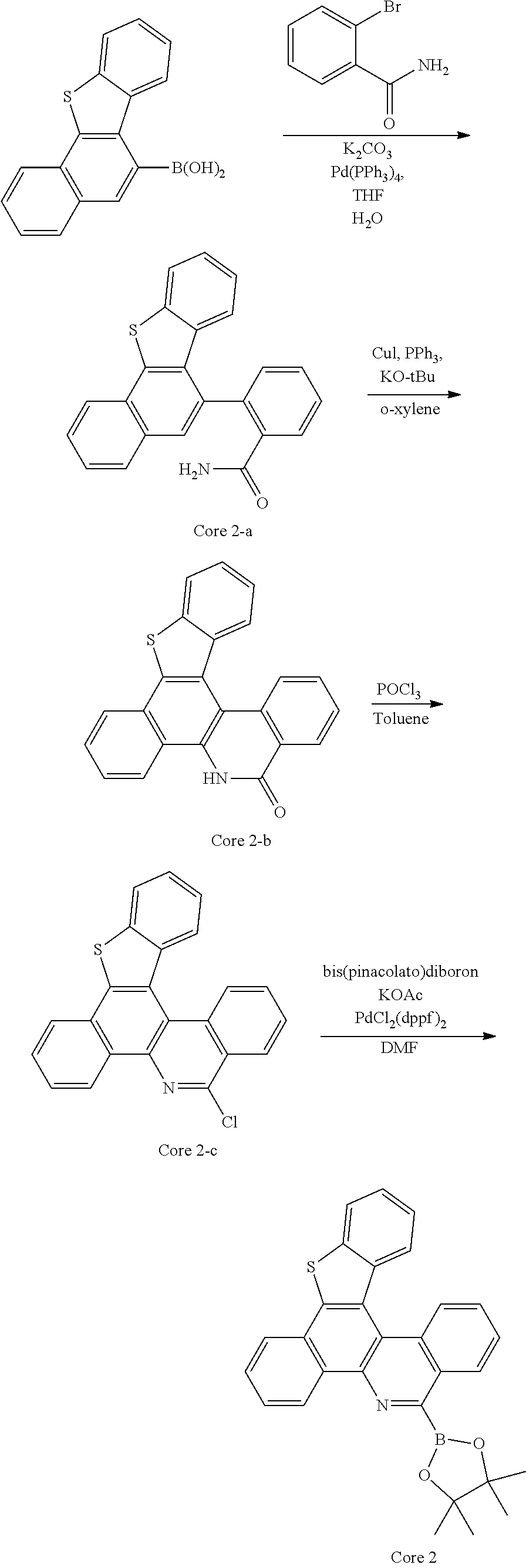


| TABLE 1 | |||
| compound | FD-MS | compound | FD-MS |
| Core 1 | m/z = 411.15(C25H22BNO2S = 411.33) | Core 2 | m/z = 461.16(C29H24BNO2S = 461.39) |
| Core 3 | m/z = 411.15(C25H22BNO2S = 411.33) | Core 4 | m/z = 461.16(C29H24BNO2S = 461.39) |
| Core 5 | m/z = 411.15(C25H22BNO2S = 411.33) | Core 6 | m/z = 411.15(C25H22BNO2S = 411.33) |
| Core 7 | m/z = 461.16(C29H24BNO2S = 461.39) | Core 8 | m/z = 461.16(C29H24BNO2S = 461.39) |
| Core 9 | m/z = 411.15(C25H22BNO2S = 411.33) | Core 10 | m/z = 411.15(C25H22BNO2S = 411.33) |


| TABLE 2 | |||
| compound | FD-MS | compound | FD-MS |
| Sub 1-1 | m/z = 267.06(C15H10ClN3 = 267.72) | Sub 1-2 | m/z = 231.99(C12H9Br = 233.11) |
| Suh 1-3 | m/z = 265.07(C17H12ClN = 265.74) | Sub 1-4 | m/z = 449.05(C26H16BrN3 = 450.34) |
| Sub 1-5 | m/z = 366.09(C24H15ClN2 = 366.85) | Sub 1-6 | m/z = 266.06(C16H11ClN2 = 266.73) |
| Suh 1-7 | m/z = 279.99(C16H9Br = 281.15) | Sub 1-8 | m/z = 499.07(C30H18BrN3 = 500.40) |
| Sub 1-9 | m/z = 269.05(C13H8ClN5 = 269.69) | Sub 1-10 | m/z = 416.11(C26H17ClN2 = 416.91) |
| Sub 1-11 | m/z = 265.07(C17H12ClN = 265.74) | Sub 1-12 | m/z = 290.06(C18H11ClN2 = 290.75) |
| Sub 1-13 | m/z = 254.06(C18H11ClN2 = 290.75) | Sub 1-14 | m/z = 321.02(C18H12BrN = 322.21) |
| Sub 1-15 | m/z = 639.16(C43H30BrN = 640.62) | Sub 1-16 | m/z = 450.05(C25H15BrN4 = 451.33) |
| Sub 1-17 | m/z = 266.06(C16H11ClN2 = 266.73) | Sub 1-18 | m/z = 266.06(C16H11ClN2 = 266.73) |
| Sub 1-19 | m/z = 450.05(C25H15BrN4 = 451.33) | Sub 1-20 | m/z = 437.05(C25H15BrN3 = 438.33) |
| Sub 1-21 | m/z = 268.05(C14H9ClN4 = 268.70) | Sub 1-22 | m/z = 437.05(C25H16BrN3 = 438.33) |
| Sub 1-23 | m/z = 296.06(C16H9ClN2S = 266.73) | Sub 1-24 | m/z = 308.02(C18H13Br = 309.21) |
| Sub 1-25 | m/z = 346.03(C20H11ClN2S = 346.83) | Sub 1-26 | m/z = 507.15(C34H22ClN3 = 508.02) |
| Sub 1-27 | m/z = 240.05(C14H9ClN2 = 240.69) | Sub 1-28 | m/z = 214.03(C12H7ClN2 = 214.65) |
| Sub 1-29 | m/z = 269.05(C13H8ClN5 = 269.69) | Sub 1-30 | m/z = 366.09(C24H15ClN2 = 366.85) |
| Sub 1-31 | m/z = 346.03(C20H11ClN2S = 346.83) | Sub 1-32 | m/z = 306.00(C18H11Br = 307.19) |
| Sub 1-33 | m/z = 337.98(C18H11BrS = 339.25) | Sub 1-34 | m/z = 213.03(C13H8ClN = 213.66) |
| Sub 1-35 | m/z = 306.00(C18H11Br = 307.19) | Sub 1-36 | m/z = 268.05(C14H9ClN4 = 268.70) |
| Sub 1-37 | m/z = 450.05(C25H15BrN4 = 451.33) | Sub 1-38 | m/z = 450.05(C25H15BrN4 = 451.33) |
| Sub 1-39 | m/z = 316.08(C20H13ClN2 = 316.79) | Sub 1-40 | m/z = 387.04(C21H14BrN3 = 388.27) |
| Sub 1-41 | m/z = 366.09(C24H15ClN2 = 366.85) | Sub 1-42 | m/z = 487.07(C29H18BrN3 = 488.39) |
| Sub 1-43 | m/z = 245.08(C14H4D5ClN2 = 245.72) | Sub 1-44 | m/z = 282.00(C16H11Br = 283.17) |
| Sub 1-45 | m/z = 372.05(C22H13ClN2S = 372.87) | Sub 1-46 | m/z = 387.04(C21H14BrN3 = 388.27) |
| Sub 1-47 | m/z = 367.09(C23H14ClN3 = 367.84) | Sub 1-48 | m/z = 316.08(C20H13ClN2 = 316.79) |
| Sub 1-49 | m/z = 449.05(C26H16BrN3 = 450.34) | Sub 1-50 | m/z = 450.05(C25H15BrN4 = 451.33) |
| Sub 1-51 | m/z = 366.09(C24H15ClN2 = 366.85) | Sub 1-52 | m/z = 450.05(C25H15BrN4 = 451.33) |
| Sub 1-53 | m/z = 290.06(C18H11ClN2 = 290.75) | Sub 1-54 | m/z = 407.12(C26H18ClN3 = 407.90) |
| Sub 1-55 | m/z = 450.05(C25H15BrN4 = 451.33) | Sub 1-56 | m/z = 450.05(C25H15BrN4 = 451.33) |
| Sub 1-57 | m/z = 346.03(C20H11ClN2S = 346.83) | Sub 1-58 | m/z = 255.99(C14H9Br = 257.13) |
| Sub 1-59 | m/z = 282.00(C16H11Br = 283.17) | Sub 1-60 | m/z = 290.06(C18H11ClN2 = 290.75) |
| Sub 1-61 | m/z = 280.04(C16H9ClN2O = 280.71) | Sub 1-62 | m/z = 346.03(C20H11ClN2S = 346.83) |
| Sub 1-63 | m/z = 333.02(C19H12BrN = 334.22) | Sub 1-64 | m/z = 280.04(C16H9ClN2O = 280.71) |
| Sub 1-65 | m/z = 423.06(C26H18BrN = 424.34) | Sub 1-66 | m/z = 372.05(C22H13ClN2S = 372.87) |
| Sub 1-67 | m/z = 330.06(C20H11ClN2O = 330.77) | Sub 1-68 | m/z = 515.12(C33H26BrN = 516.48) |
| Sub 1-69 | m/z = 296.02(C16H9ClN2S = 296.77) | Sub 1-70 | m/z = 373.05(C22H16BrN = 374.28) |
| Sub 1-71 | m/z = 321.02(C16H12BrN = 322.21) | Sub 1-72 | m/z = 282.00(C16H11Br = 283.17) |
| Sub 1-73 | m/z = 340.08(C22H13ClN2 = 340.81) | Sub 1-74 | m/z = 337.08(C18H11BrS = 340.81) |
| Sub 1-75 | m/z = 439.09(C27H22BrN = 440.38) | Sub 1-76 | m/z = 333.02(C19H12BrN = 334.22) |


| TABLE 3 | |||
| compound | FD-MS | compound | FD-MS |
| P-1-1 | m/z = 516.14(C34H20N4S = 516.62) | P-1-2 | m/z = 514.15(C36H22N2S = 515.65) |
| P-1-3 | m/z = 517.14(C33 H19N5S = 517.61) | P-1-4 | m/z = 515.15(C35H21N3S = 515.63) |
| P-1-5 | m/z = 642.19(C44H26N4S = 642.78) | P-1-6 | m/z = 592.17(C40H24N4S = 592.72) |
| P-1-7 | m/z = 517.14(C33H19N5S = 517.61) | P-1-8 | m/z = 489.13(C33H19N3S = 489.60) |
| P-1-9 | m/z = 595.12(C39H21N3S2 = 595.74) | P-1-10 | m/z = 665.19(C47H27N3S = 665.81) |
| P-1-11 | m/z = 565.16(C39H23N3S = 565.69) | P-1-12 | m/z = 539.15(C37H21N3S = 539.66) |
| P-1-13 | m/z = 656.20(C45H28N4S = 656.81) | P-1-14 | m/z = 539.15(C37H21N3S = 539.66) |
| P-1-15 | m/z = 545.10(C35H19N3S2 = 5453.68) | P-1-16 | m/z = 513.15(C35H19N3O2 = 513.56) |
| P-1-17 | m/z = 828.31(C62H40N2O = 829.02) | P-1-18 | m/z = 638.21(C45H26N4O = 638.73) |
| P-1-19 | m/z = 688.23(C49H28N4O = 688.79) | P-1-20 | m/z = 639.21(C44H25N5O = 639.72) |
| P-2-1 | m/z = 566.16(C38H22N4S = 566.68) | P-2-2 | m/z = 564.17(C36H20N6S = 564.71) |
| P-2-3 | m/z = 568.15(C36H20N6S = 568.66) | P-2-4 | m/z = 565.16(C39H23N3S = 565.69) |
| P-2-5 | m/z = 642.19(C44H26N4S = 642.78) | P-2-6 | m/z = 642.19(C44H26N4S = 642.78) |
| P-2-7 | m/z = 565.16(C39H23N3S = 565.69) | P-2-8 | m/z = 539.15(C17H21N3S = 539.66) |
| P-2-9 | m/z = 645.13(C43H23N3S2 = 645.80) | P-2-10 | m/z = 589.16(C41H23N3S = 589.72) |
| P-2-11 | m/z = 615.18(C43H25N3S = 615.75) | P-2-12 | m/z = 589.16(C41H23N3S = 589.72) |
| P-2-13 | m/z = 706.22(C49H30N4S = 706.87) | P-2-14 | m/z = 589.16(C41H23N3S = 589.72) |
| P-2-15 | m/z = 645.13(C43H23N3S2 = 645.80) | P-2-16 | m/z = 563.16(C39H21N3O2 = 563.62) |
| P-2-17 | m/z = 754.30(C56H38N2O = 754.93) | P-2-18 | m/z = 688.23(C49H28N4O = 688.79) |
| P-2-19 | m/z = 689.22(C48H27N5O = 689.78) | P-2-20 | m/z = 689.22(C38H27N5O = 689.78) |
| P-3-1 | m/z = 592.17(C40H24N4S = 592.72) | P-3-2 | m/z = 515.15(C35H21N3S = 515.63) |
| P-3-3 | m/z = 489.13(C33H19N3S = 489.13) | P-3-4 | m/z = 595.12(C39H21N3S2 = 595.74) |
| P-3-5 | m/z = 615.18(C43H25N3S = 615.75) | P-3-6 | m/z = 565.16(C39H23N3S = 565.69) |
| P-3-7 | m/z = 539.15(C37H21N3S = 539.66) | P-3-8 | m/z = 656.20(C45H28N4S = 656.81) |
| P-3-9 | m/z = 539.15(C37H21N3S = 539.66) | P-3-10 | m/z = 545.10(C35H19N3S2 = 545.68) |
| P-3-11 | m/z = 529.12(C35H19N3OS = 529.62) | P-3-12 | m/z = 644.23(C46H32N2S = 644.84) |
| P-3-13 | m/z = 654.19(C45H26N4S = 654.79) | P-3-14 | m/z = 655.18(C44H25N5S = 655.78) |
| P-3-15 | m/z = 655.18(C44H25N5S = 655.78) | P-3-16 | m/z = 471.16(C35H21NO = 471.56) |
| P-3-17 | m/z = 497.18(C37H23NO = 497.60) | P-3-18 | m/z = 522.17(C38H22N2O = 522.61) |
| P-3-19 | m/z = 445.15(C33H19NO = 445.52) | P-3-20 | m/z = 527.13(C37H21NOS = 527.64) |
| P-4-1 | m/z = 566.16(C38H22N4S = 566.68) | P-4-2 | m/z = 564.17(C40H24N2S = 564.71) |
| P-4-3 | m/z = 567.15(C37H21N5S = 567.67) | P-4-4 | m/z = 565.16(C39H23N3S = 565.69) |
| P-4-5 | m/z = 692.20(C48H28N4S = 692.84) | P-4-6 | m/z = 642.19(C44H26N4S = 642.78) |
| P-4-7 | m/z = 565.16(C39H23N3S = 565.69) | P-4-8 | m/z = 544.18(C37H16D5N3S = 544.69) |
| P-4-9 | m/z = 553.16(C38H23N3S = 553.68) | P-4-10 | m/z = 645.13(C43H23N3S2 = 645.80) |
| P-4-11 | m/z = 629.16(C43H23N3OS = 629.74) | P-4-12 | m/z = 628.20(C45H28N2S = 628.79) |
| P-4-13 | m/z = 704.20(C49H28N4S = 704.85) | P-4-14 | m/z = 705.20(C48H27N5S = 705.84) |
| P-4-15 | m/z = 705.20(C48H27N5S = 705.84) | P-4-16 | m/z = 519.16(C39H21NO = 519.60) |
| P-4-17 | m/z = 560.19(C41H24N2O = 560.66) | P-4-18 | m/z = 496.16(C36H20N2O = 496.57) |
| P-4-19 | m/z = 579.14(C39H21N3OS = 579.68) | P-4-20 | m/z = 550.18(C38H22N4O = 550.62) |
| P-5-1 | m/z = 516.14(C34H20N4S = 516.62) | P-5-2 | m/z = 515.15(C35H21N3S = 515.63) |
| P-5-3 | m/z = 518.13(C32H18N6S = 518.60) | P-5-4 | m/z = 515.15(C35H21N3S = 515.63) |
| P-5-5 | m/z = 592.17(C40H24N4S = 592.72) | P-5-6 | m/z = 565.16(C39H23N3S = 565.69) |
| P-5-7 | m/z = 539.15(C37H21N3S = 539.66) | P-5-8 | m/z = 656.20(C45H28N4S = 656.81) |
| P-5-9 | m/z = 539.15(C37H21N3S = 539.66) | P-5-10 | m/z = 595.12(C39H21N3S2 = 595.74) |
| P-5-11 | m/z = 579.14(C39H21N3OS = 579.68) | P-5-12 | m/z = 628.20(C45H28N2S = 628.79) |
| P-5-13 | m/z = 654.19(C45H26N4S = 654.79) | P-5-14 | m/z = 655.18(C44H25N5S = 655.78) |
| P-5-15 | m/z = 655.18(C44H25N5S = 655.78) | P-5-16 | m/z = 471.16(C35H21NO = 471.56) |
| P-5-17 | m/z = 498.17(C36H22N2O = 498.59) | P-5-18 | m/z = 473.15(C33H19N3O = 473.54) |
| P-5-19 | m/z = 447. 14(C31H17N3O = 447.50) | P-5-20 | m/z = 527.13(C37H21NOS = 527.64) |
| P-6-1 | m/z = 516.14(C34H20N4S = 516.62) | P-6-2 | m/z = 615.18(C43H25N3S = 615.75) |
| P-6-3 | m/z = 616.14(C42H24N4S = 616.74) | P-6-4 | m/z = 515.15(C35H21N3S = 515.63) |
| P-6-5 | m/z = 642.19(C44H26N4S = 642.78) | P-6-6 | m/z = 592.17(C40H24N4S = 592.72) |
| P-6-7 | m/z = 515.15(C35H21N3S = 515.63) | P-6-8 | m/z = 489.13(C33H19N3S = 489.60) |
| P-6-9 | m/z = 595.12(C39H21N3S2 = 595.74) | P-6-10 | m/z = 615.18(C43H25N3S = 615.75) |
| P-6-11 | m/z = 565.16(C39H23N3S = 565.69) | P-6-12 | m/z = 539.15(C37H21N3S = 539.66) |
| P-6-13 | m/z = 756.23(C53H32N4S = 756.93) | P-6-14 | m/z = 589.16((C41H23N3S = 589.72) |
| P-6-15 | m/z = 545.10(C35H19N3S2 = 545.68) | P-6-16 | m/z = 513.15(C35H19N3O2 = 513.56) |
| P-6-17 | m/z = 828.31(C62H40N2O = 829.02) | P-6-18 | m/z = 638.21(C45H26N4O = 638.73) |
| P-6-19 | m/z = 688.23(C49H28N4O = 688.79) | P-6-20 | m/z = 639.21(C44H25N5O = 639.72) |
| P-7-1 | m/z = 642.19(C44H26N4S = 642.78) | P-7-2 | m/z = 565.16(C39H23N3S = 565.69) |
| P-7-3 | m/z = 544.18(C37H16D5N3S = 544.69) | P-7-4 | m/z = 553.16(C38H23N3S = 553.68) |
| P-7-5 | m/z = 645.13(C43H23N3S2 = 645.80) | P-7-6 | m/z = 615.18(C43H25N3S = 675.75) |
| P-7-7 | m/z = 589.16(C41H23N3S = 589.72) | P-7-8 | m/z = 706.22(C49H30N4S = 706.87) |
| P-7-9 | m/z = 589.16(C41H23N3S = 589.72) | P-7-10 | m/z = 645.13(C43H23N3S2 = 645.80) |
| P-7-11 | m/z = 629.16(C43H23N3OS = 629.74) | P-7-12 | m/z = 628.20(C45H28N2S = 628.79) |
| P-7-13 | m/z = 704.20(C49H28N4S = 704.85) | P-7-14 | m/z = 705.20(C48H27N5S = 705.84) |
| P-7-15 | m/z = 705.20(C48H27N5S = 705.84) | P-7-16 | m/z = 519.16(C39H21NO = 519.60) |
| P-7-17 | m/z = 560.19(C39H21NO = 560.60) | P-7-18 | m/z = 496.16(C36H20N2O = 496.57) |
| P-7-19 | m/z = 523.17(C37H21N3O = 523.60) | P-7-20 | m/z = 550.18(C38H22N4O = 550.62) |
| P-8-1 | m/z = 566.16(C38H22N4S = 566.68) | P-8-2 | m/z = 564.17(C40H24N2S = 564.71) |
| P-8-3 | m/z = 568.16(C36H20N6S = 568.66) | P-8-4 | m/z = 565.16(C39H23N3S = 565.69) |
| P-8-5 | m/z = 642.19(C44H26N4S = 642.78) | P-8-6 | m/z = 642.19(C44H26N4S = 642.78) |
| P-8-7 | m/z = 565.16(C39H23N3S = 565.69) | P-8-8 | m/z = 539.15(C37H21N3S = 539.66) |
| P-8-9 | m/z = 645.13(C43H23N3S2 = 645.80) | P-8-10 | m/z = 665.19(C47H27N3S = 665.81) |
| P-8-11 | m/z = 579.14(C39H21N3OS = 579.68) | P-8-12 | m/z = 694.24(C50H34N2S = 694.90) |
| P-8-13 | m/z = 704.20(C49H28N4S = 704.85) | P-8-14 | m/z = 705.20(C48H27N5S = 705.84) |
| P-8-15 | m/z = 705.20(C48N27N5S = 705.84) | P-8-16 | m/z = 521.18(C39H23NO = 521.62) |
| P-8-17 | m/z = 547.19(C41H25NO = 547.66) | P-8-18 | m/z = 572.19(C42H24N2O = 572.67) |
| P-8-19 | m/z = 495.16(C37H21NO = 495.58) | P-8-20 | m/z = 577.15(C41H23NOS = 577.70) |
| P-9-1 | m/z = 516.14(C34H20N4S = 516.62) | P-9-2 | m/z = 515.15(C35H21N3S = 515.63) |
| P-9-3 | m/z = 518.13(C32H18N6S = 518.60) | P-9-4 | m/z = 515.15(C35H21N3S = 515.63) |
| P-9-5 | m/z = 692.20(C48H28N4S = 692.84) | P-9-6 | m/z = 565.16(C39H23N3S = 565.69) |
| P-9-7 | m/z = 539.15(C37H21N3S = 539.66) | P-9-8 | m/z = 656.20(C45H28N4S = 656.81) |
| P-9-9 | m/z = 621.13(C41H23N3S2 = 621.78) | P-9-10 | m/z = 595.12(C39H21N3S2 = 595.74) |
| P-9-11 | m/z = 621.13(C41H23N3S2 = 621.78) | P-9-12 | m/z = 628.20(C45H28N2S = 628.79) |
| P-9-13 | m/z = 654.19(C45H26N4S = 654.79) | P-9-14 | m/z = 655.18(C44H25N5S = 655.78) |
| P-9-15 | m/z = 655.18(C44H25N5S = 655.78) | P-9-16 | m/z = 471.16(C35H21NO = 471.56) |
| P-9-17 | m/z = 498.17(C36H22N2O = 498.59) | P-9-18 | m/z = 522.17(C38H22N2O = 522.61) |
| P-9-19 | m/z = 447.14(C31H17N3O = 447.50) | P-9-20 | m/z = 527.13(C37H21NOS = 527.64) |
| P-10-1 | m/z = 516.14(C34H20N4S = 516.62) | P-10-2 | m/z = 515.15(C35H21N3S = 515.63) |
| P-10-3 | m/z = 518.13(C32H18N6S = 518.60) | P-10-4 | m/z = 515.15(C35H21N3S = 515.63) |
| P-10-5 | m/z = 592.17(C40H24N4S = 592.72) | P-10-6 | m/z = 592.17(C40H24N4S = 592.72) |
| P-10-7 | m/z = 515.15(C35H21N3S = 515.63) | P-10-8 | m/z = 489.13(C33H19N3S = 489.60) |
| P-10-9 | m/z = 595.12(C39H21N3S = 595.74) | P-10-10 | m/z = 615.18(C43H25N3S = 615.75) |
| P 10 11 | m/z = 565.16(C39H23N3S = 565.69) | P-10-12 | m/z = 539.15(C37H21N3S = 539.66) |
| P-10-13 | m/z = 656.20(C45H28N4S = 656.81) | P-10-14 | m/z = 539.15(C37H21N3S = 539.66) |
| P-10-15 | m/z = 545.10(C35H19N3S2 = 545.68) | P-10-16 | m/z = 522.17(C38H22N2O = 522.61) |
| P-10-17 | m/z = 421.15(C31H19NO = 421.50) | P-10-18 | m/z = 471.16(C35H21NO = 471.56) |
| P-10-19 | m/z = 495.16(C37H21NO = 495.58) | P-10-20 | m/z = 495.16(C37H21NO = 495.58) |

| TABLE 4 | ||||||||
| Current | ||||||||
| Vo1tage | Density | Brightness | Efficiency | Lifetime | CIE | |||
| compound | (V) | (mA/cm2) | (cd/m2) | (cd/A) | T(95) | (x, y) | ||
| comp. Ex (1) | Com. (A) | 6.2 | 34.7 | 2500.0 | 7.2 | 69.1 | (0.66, 0.32) |
| comp. Ex (2) | Com. (B) | 5.7 | 32.5 | 2500.0 | 7.7 | 73.1 | (0.67, 0.32) |
| comp. Ex (3) | Com. (C) | 5.5 | 30.1 | 2500.0 | 8.3 | 90.8 | (0.66, 0.32) |
| comp. Ex (4) | Com. (D) | 5.3 | 27.5 | 2500.0 | 9.1 | 96.4 | (0.66, 0.35) |
| comp. Ex (5) | Com. (E) | 5.1 | 26.3 | 2500.0 | 9.5 | 98.1 | (0.66, 0.35) |
| Ex. (1) | Com. (P-1-1) | 4.6 | 17.8 | 2500.0 | 14.0 | 112.5 | (0.65, 0.35) |
| Ex. (2) | Com. (P-1-8) | 4.5 | 17.9 | 2500.0 | 14.0 | 112.5 | (0.65, 0.35) |
| Ex. (3) | Com. (P-1-14) | 4.6 | 18.5 | 2500.0 | 13.5 | 110.7 | (0.66, 0.35) |
| Ex. (4) | Com. (P-1-15) | 4.6 | 19.3 | 2500.0 | 13.0 | 118.3 | (0.66, 0.35) |
| Ex. (5) | Com. (P-1-18) | 4.8 | 17.2 | 2500.0 | 14.5 | 118.5 | (0.66, 0.35) |
| Ex. (6) | Com. (P-2-1) | 4.4 | 15.4 | 2500.0 | 16.2 | 121.3 | (0.66, 0.35) |
| Ex. (7) | Com. (P-2-8) | 4.4 | 16.4 | 2500.0 | 15.3 | 127.1 | (0.66, 0.35) |
| Ex. (8) | Com. (P-2-14) | 4.5 | 16.3 | 2500.0 | 15.3 | 121.0 | (0.66, 0.35) |
| Ex. (9) | Com. (P-2-15) | 4.4 | 16.1 | 2500.0 | 15.6 | 120.1 | (0.66, 0.35) |
| Ex. (10) | Com. (P-2-18) | 4.4 | 15.4 | 2500.0 | 16.3 | 120.3 | (0.66, 0.35) |
| Ex. (11) | Com. (P-3-1) | 4.6 | 18.6 | 2500.0 | 13.5 | 112.4 | (0.66, 0.35) |
| Ex. (12) | Com. (P-3-8) | 4.5 | 20.0 | 2500.0 | 12.5 | 110.8 | (0.66, 0.35) |
| Ex. (13) | Com. (P-3-14) | 4.6 | 20.3 | 2500.0 | 12.3 | 113.4 | (0.66, 0.35) |
| Ex. (14) | Com. (P-3-15) | 4.7 | 18.1 | 2500.0 | 13.8 | 116.6 | (0.66, 0.35) |
| Ex. (15) | Com. (P-3-18) | 4.7 | 18.9 | 2500.0 | 13.2 | 112.5 | (0.66, 0.35) |
| Ex. (16) | Com. (P-4-1) | 4.5 | 15.0 | 2500.0 | 16.6 | 127.3 | (0.66, 0.35) |
| Ex. (17) | Com. (P-4-8) | 4.4 | 15.3 | 2500.0 | 16.3 | 122.1 | (0.66, 0.35) |
| Ex. (18) | Com. (P-4-14) | 4.3 | 15.3 | 2500.0 | 16.3 | 126.8 | (0.66, 0.35) |
| Ex. (19) | Com. (P-4-15) | 4.4 | 16.2 | 2500.0 | 15.4 | 126.5 | (0.66, 0.35) |
| Ex. (20) | Com. (P-4-18) | 4.5 | 15.8 | 2500.0 | 15.9 | 128.6 | (0.66, 0.35) |
| Ex. (21) | Com. (P-5-1) | 4.8 | 18.3 | 2500.0 | 13.7 | 115.2 | (0.66, 0.35) |
| Ex. (22) | Com. (P-5-8) | 4.6 | 18.8 | 2500.0 | 13.3 | 119.5 | (0.66, 0.35) |
| Ex. (23) | Com. (P-5-14) | 4.7 | 18.1 | 2500.0 | 13.8 | 114.6 | (0.66, 0.35) |
| Ex. (24) | Com. (P-5-15) | 4.6 | 17.1 | 2500.0 | 14.7 | 118.3 | (0.66, 0.35) |
| Ex. (25) | Com. (P-5-18) | 4.5 | 20.4 | 2500.0 | 12.2 | 112.6 | (0.66, 0.35) |
| Ex. (26) | Com. (P-6-1) | 4.7 | 17.2 | 2500.0 | 14.5 | 119.0 | (0.66, 0.35) |
| Ex. (27) | Com. (P-6-8) | 4.6 | 17.0 | 2500.0 | 14.7 | 118.2 | (0.66, 0.35) |
| Ex. (28) | Com. (P-6-14) | 4.8 | 19.6 | 2500.0 | 12.8 | 111.7 | (0.66, 0.35) |
| Ex. (29) | Com. (P-6-15) | 4.5 | 18.8 | 2500.0 | 13.3 | 119.2 | (0.66, 0.35) |
| Ex. (30) | Com. (P-6-18) | 4.5 | 18.3 | 2500.0 | 13.6 | 115.9 | (0.66, 0.35) |
| Ex. (31) | Com. (P-7-1) | 4.4 | 15.9 | 2500.0 | 15.8 | 122.8 | (0.66, 0.35) |
| Ex. (32) | Com. (P-7-8) | 4.3 | 14.9 | 2500.0 | 16.8 | 123.8 | (0.66, 0.35) |
| Ex. (33) | Com. (P-7-14) | 4.4 | 15.6 | 2500.0 | 16.1 | 127.5 | (0.66, 0.35) |
| Ex. (34) | Com. (P-7-15) | 4.5 | 15.6 | 2500.0 | 16.1 | 128.0 | (0.66, 0.35) |
| Ex. (35) | Com. (P-7-18) | 4.4 | 15.7 | 2500.0 | 15.9 | 120.5 | (0.66, 0.35) |
| Ex. (36) | Com. (P-8-1) | 4.4 | 16.1 | 2500.0 | 15.5 | 120.5 | (0.66, 0.35) |
| Ex. (37) | Com. (P-8-8) | 4.4 | 14.9 | 2500.0 | 16.8 | 121.9 | (0.66, 0.35) |
| Ex. (38) | Com. (P-8-14) | 4.3 | 15.6 | 2500.0 | 16.1 | 121.7 | (0.66, 0.35) |
| Ex. (39) | Com. (P-8-15) | 4.4 | 15.8 | 2500.0 | 15.8 | 120.5 | (0.66, 0.35) |
| Ex. (40) | Com. (P-8-18) | 4.4 | 14.8 | 2500.0 | 16.9 | 129.0 | (0.66, 0.35) |
| Ex. (41) | Com. (P-9-1) | 4.6 | 20.2 | 2500.0 | 12.4 | 119.5 | (0.66, 0.35) |
| Ex. (42) | Com. (P-9-8) | 4.7 | 19.0 | 2500.0 | 13.2 | 118.5 | (0.66, 0.35) |
| Ex. (43) | Com. (P-9-14) | 4.7 | 18.5 | 2500.0 | 13.5 | 116.6 | (0.66, 0.35) |
| Ex. (44) | Com. (P-9-15) | 4.6 | 17.3 | 2500.0 | 14.5 | 119.2 | (0.66, 0.35) |
| Ex. (45) | Com. (P-9-18) | 4.7 | 17.1 | 2500.0 | 14.6 | 115.4 | (0.66, 0.35) |
| Ex. (46) | Com. (P-10-1) | 4.6 | 17.5 | 2500.0 | 14.3 | 119.6 | (0.66, 0.35) |
| Ex. (47) | Com. (P-10-8) | 4.7 | 18.4 | 2500.0 | 13.6 | 112.8 | (0.66, 0.35) |
| Ex. (48) | Com. (P-10-14) | 4.8 | 19.1 | 2500.0 | 13.1 | 113.9 | (0.66, 0.35) |
| Ex. (49) | Com. (P-10-15) | 4.5 | 18.0 | 2500.0 | 13.9 | 115.1 | (0.66, 0.35) |
| Ex. (50) | Com. (P-10-18) | 4.7 | 16.9 | 2500.0 | 14.8 | 117.6 | (0.66, 0.35) |
Claims (11)


Applications Claiming Priority (3)
| Application Number | Priority Date | Filing Date | Title |
|---|---|---|---|
| KR1020150127670A KR102370155B1 (en) | 2015-09-09 | 2015-09-09 | Compound for organic electronic element, organic electronic element comprising the same, and electronic device thereof |
| KR10-2015-0127670 | 2015-09-09 | ||
| PCT/KR2016/009642 WO2017043797A1 (en) | 2015-09-09 | 2016-08-30 | Compound for organic electronic element, organic electronic element using same, and electronic device thereof |
Publications (2)
| Publication Number | Publication Date |
|---|---|
| US20200223835A1 US20200223835A1 (en) | 2020-07-16 |
| US10968208B2 true US10968208B2 (en) | 2021-04-06 |
Family
ID=58240018
Family Applications (1)
| Application Number | Title | Priority Date | Filing Date |
|---|---|---|---|
| US15/758,827 Active 2037-10-12 US10968208B2 (en) | 2015-09-09 | 2016-08-30 | Compound for organic electronic element, organic electronic element comprising the same, and electronic device thereof |
Country Status (4)
| Country | Link |
|---|---|
| US (1) | US10968208B2 (en) |
| KR (1) | KR102370155B1 (en) |
| CN (1) | CN108026111B (en) |
| WO (1) | WO2017043797A1 (en) |
Families Citing this family (4)
| Publication number | Priority date | Publication date | Assignee | Title |
|---|---|---|---|---|
| WO2019049965A1 (en) * | 2017-09-11 | 2019-03-14 | 保土谷化学工業株式会社 | Compound having pyrimidine ring structure and organic electroluminescent element |
| KR102531632B1 (en) * | 2017-12-26 | 2023-05-12 | 엘티소재주식회사 | Heterocyclic compound and organic light emitting device comprising the same |
| CN111675707B (en) * | 2019-03-10 | 2023-06-06 | 北京夏禾科技有限公司 | Organic electroluminescent material and device thereof |
| CN111548350A (en) * | 2020-04-16 | 2020-08-18 | 苏州久显新材料有限公司 | Polycyclic aromatic hydrocarbon aza-naphthalene derivative, synthetic method and electronic device thereof |
Citations (6)
| Publication number | Priority date | Publication date | Assignee | Title |
|---|---|---|---|---|
| US20040122230A1 (en) * | 2002-09-18 | 2004-06-24 | The Curators Of The University Of Missouri | Opiate analogs selective for the delta -opioid receptor |
| WO2010114264A2 (en) | 2009-03-31 | 2010-10-07 | Dow Advanced Display Materials,Ltd. | Novel organic electroluminescent compounds and organic electroluminescent device using the same |
| KR20120096383A (en) | 2011-02-22 | 2012-08-30 | (주)씨에스엘쏠라 | Organic light compound and organic light device using the same |
| KR20120116879A (en) | 2011-04-13 | 2012-10-23 | 에스에프씨 주식회사 | Condensed aryl compounds and organic light-diode including the same |
| CN103058987A (en) | 2011-10-19 | 2013-04-24 | 三星显示有限公司 | Condensed-cyclic compound, method for preparing the condensed-cyclic compound and organic light-emitting device including the condensed-cyclic compound |
| KR20130053846A (en) | 2011-11-16 | 2013-05-24 | 롬엔드하스전자재료코리아유한회사 | Novel organic electroluminescence compounds and organic electroluminescence device using the same |
Family Cites Families (2)
| Publication number | Priority date | Publication date | Assignee | Title |
|---|---|---|---|---|
| KR101472295B1 (en) * | 2011-12-19 | 2014-12-15 | 단국대학교 산학협력단 | Multicyclic aromatic compound and organic light emitting device including the same |
| KR102098063B1 (en) * | 2013-05-21 | 2020-04-07 | 덕산네오룩스 주식회사 | Compound for organic electronic element, organic electronic element using the same, and an electronic device thereof |
-
2015
- 2015-09-09 KR KR1020150127670A patent/KR102370155B1/en active IP Right Grant
-
2016
- 2016-08-30 WO PCT/KR2016/009642 patent/WO2017043797A1/en active Application Filing
- 2016-08-30 CN CN201680052331.7A patent/CN108026111B/en active Active
- 2016-08-30 US US15/758,827 patent/US10968208B2/en active Active
Patent Citations (8)
| Publication number | Priority date | Publication date | Assignee | Title |
|---|---|---|---|---|
| US20040122230A1 (en) * | 2002-09-18 | 2004-06-24 | The Curators Of The University Of Missouri | Opiate analogs selective for the delta -opioid receptor |
| WO2010114264A2 (en) | 2009-03-31 | 2010-10-07 | Dow Advanced Display Materials,Ltd. | Novel organic electroluminescent compounds and organic electroluminescent device using the same |
| KR20100108924A (en) | 2009-03-31 | 2010-10-08 | 다우어드밴스드디스플레이머티리얼 유한회사 | Novel organic electroluminescent compounds and organic electroluminescent device using the same |
| KR20120096383A (en) | 2011-02-22 | 2012-08-30 | (주)씨에스엘쏠라 | Organic light compound and organic light device using the same |
| KR20120116879A (en) | 2011-04-13 | 2012-10-23 | 에스에프씨 주식회사 | Condensed aryl compounds and organic light-diode including the same |
| CN103058987A (en) | 2011-10-19 | 2013-04-24 | 三星显示有限公司 | Condensed-cyclic compound, method for preparing the condensed-cyclic compound and organic light-emitting device including the condensed-cyclic compound |
| US20130099208A1 (en) | 2011-10-19 | 2013-04-25 | Samsung Mobile Display Co., Ltd. | Condensed-cyclic compound, method for preparing the condensed-cyclic compound and organic light-emitting device including the condensed-cyclic compound |
| KR20130053846A (en) | 2011-11-16 | 2013-05-24 | 롬엔드하스전자재료코리아유한회사 | Novel organic electroluminescence compounds and organic electroluminescence device using the same |
Non-Patent Citations (1)
| Title |
|---|
| Chinese Office Action for corresponding Chinese Patent Application No. 201680052331.7, dated Nov. 1, 2019, seven pages. |
Also Published As
| Publication number | Publication date |
|---|---|
| KR102370155B1 (en) | 2022-03-04 |
| CN108026111A (en) | 2018-05-11 |
| CN108026111B (en) | 2021-03-12 |
| KR20170030291A (en) | 2017-03-17 |
| US20200223835A1 (en) | 2020-07-16 |
| WO2017043797A1 (en) | 2017-03-16 |
Similar Documents
| Publication | Publication Date | Title |
|---|---|---|
| US10319923B2 (en) | Compound for organic electronic element, organic electronic element comprising the same and electronic device thereof | |
| US9530971B1 (en) | Compound for organic electric element, organic electric element comprising the same and electronic device thereof | |
| US11299459B2 (en) | Compound for organic electric element, organic electric element comprising the same and electronic device thereof | |
| US11691966B2 (en) | Compound for organic electronic element, organic electronic element using the same, and an electronic device thereof | |
| US9799835B2 (en) | Compound for organic electric element, organic electric element comprising the same and electronic device thereof | |
| CN106573938B (en) | Compound for organic electronic element, and organic electronic element and electronic device using same | |
| US10840457B2 (en) | Compound for organic electric element, organic electric element comprising the same and electronic device thereof | |
| US11339132B2 (en) | Compound for organic electric element, organic electric element comprising the same, and electronic device thereof | |
| US11557729B2 (en) | Compound for organic electronic element, organic electronic device using same, and electronic device thereof | |
| US10658597B2 (en) | Organic electronic element comprising compound for organic electronic element, and electronic device thereof | |
| US20210098706A1 (en) | Organic electric element comprising compound for organic electric element and electronic device thereof | |
| US10468606B2 (en) | Compound for organic electric element, organic electric element comprising the same, and electronic device thereof | |
| US10428084B2 (en) | Compound for organic electric element, organic electric element comprising the same and electronic device thereof | |
| US10283716B2 (en) | Compound for organic electric element, organic electric element using the same, and electronic device comprising same | |
| US11271175B2 (en) | Organic electronic element comprising compound for organic electronic element, and electronic device thereof | |
| US11793070B2 (en) | Compound for organic electronic element, organic electronic element using the same, and electronic device thereof | |
| US20190241548A1 (en) | Compound for organic electronic element, organic electronic element using same, and electronic device comprising same | |
| US10968208B2 (en) | Compound for organic electronic element, organic electronic element comprising the same, and electronic device thereof | |
| US20220123224A1 (en) | Compound for organic electronic element, organic electronic element using the same, and an electronic device thereof | |
| US10797247B2 (en) | Compound for organic electric element, organic electric element comprising the same and electronic device thereof | |
| US11024812B2 (en) | Compound for organic-electric element, organic-electric element using same, and electronic device for same | |
| KR20160005944A (en) | Compound for organic electronic element, organic electronic element using the same, and an electronic device thereof | |
| US9871207B2 (en) | Compound for organic electric element, organic electric element comprising the same and electronic device thereof | |
| US10934308B2 (en) | Compound for organic electronic element, organic electronic element using same, and electronic device comprising same | |
| US11557732B2 (en) | Organic electroluminescent compound, and organic electroluminescent element and device employing the same |
Legal Events
| Date | Code | Title | Description |
|---|---|---|---|
| AS | Assignment |
Owner name: DUK SAN NEOLUX CO., LTD., KOREA, REPUBLIC OF Free format text: ASSIGNMENT OF ASSIGNORS INTEREST;ASSIGNORS:JANG, JAE WAN;KIM, WONSAM;PARK, BO RAM;AND OTHERS;SIGNING DATES FROM 20180130 TO 20180202;REEL/FRAME:045156/0584 |
|
| FEPP | Fee payment procedure |
Free format text: ENTITY STATUS SET TO UNDISCOUNTED (ORIGINAL EVENT CODE: BIG.); ENTITY STATUS OF PATENT OWNER: SMALL ENTITY |
|
| STPP | Information on status: patent application and granting procedure in general |
Free format text: RESPONSE TO NON-FINAL OFFICE ACTION ENTERED AND FORWARDED TO EXAMINER |
|
| STPP | Information on status: patent application and granting procedure in general |
Free format text: NOTICE OF ALLOWANCE MAILED -- APPLICATION RECEIVED IN OFFICE OF PUBLICATIONS |
|
| FEPP | Fee payment procedure |
Free format text: ENTITY STATUS SET TO SMALL (ORIGINAL EVENT CODE: SMAL); ENTITY STATUS OF PATENT OWNER: SMALL ENTITY |
|
| STPP | Information on status: patent application and granting procedure in general |
Free format text: AWAITING TC RESP, ISSUE FEE PAYMENT VERIFIED |
|
| STPP | Information on status: patent application and granting procedure in general |
Free format text: PUBLICATIONS -- ISSUE FEE PAYMENT VERIFIED |
|
| STPP | Information on status: patent application and granting procedure in general |
Free format text: AWAITING TC RESP, ISSUE FEE PAYMENT VERIFIED |
|
| STPP | Information on status: patent application and granting procedure in general |
Free format text: PUBLICATIONS -- ISSUE FEE PAYMENT VERIFIED |
|
| STCF | Information on status: patent grant |
Free format text: PATENTED CASE |
|
| CC | Certificate of correction |