US10965331B2 - Broad range voltage-controlled oscillator - Google Patents
Broad range voltage-controlled oscillator Download PDFInfo
- Publication number
- US10965331B2 US10965331B2 US16/835,052 US202016835052A US10965331B2 US 10965331 B2 US10965331 B2 US 10965331B2 US 202016835052 A US202016835052 A US 202016835052A US 10965331 B2 US10965331 B2 US 10965331B2
- Authority
- US
- United States
- Prior art keywords
- pair
- configuration
- signal
- frequency
- inductive
- Prior art date
- Legal status (The legal status is an assumption and is not a legal conclusion. Google has not performed a legal analysis and makes no representation as to the accuracy of the status listed.)
- Active
Links
Images


Classifications
-
- H—ELECTRICITY
- H03—ELECTRONIC CIRCUITRY
- H03K—PULSE TECHNIQUE
- H03K21/00—Details of pulse counters or frequency dividers
-
- H—ELECTRICITY
- H03—ELECTRONIC CIRCUITRY
- H03B—GENERATION OF OSCILLATIONS, DIRECTLY OR BY FREQUENCY-CHANGING, BY CIRCUITS EMPLOYING ACTIVE ELEMENTS WHICH OPERATE IN A NON-SWITCHING MANNER; GENERATION OF NOISE BY SUCH CIRCUITS
- H03B5/00—Generation of oscillations using amplifier with regenerative feedback from output to input
- H03B5/08—Generation of oscillations using amplifier with regenerative feedback from output to input with frequency-determining element comprising lumped inductance and capacitance
- H03B5/12—Generation of oscillations using amplifier with regenerative feedback from output to input with frequency-determining element comprising lumped inductance and capacitance active element in amplifier being semiconductor device
- H03B5/1237—Generation of oscillations using amplifier with regenerative feedback from output to input with frequency-determining element comprising lumped inductance and capacitance active element in amplifier being semiconductor device comprising means for varying the frequency of the generator
- H03B5/124—Generation of oscillations using amplifier with regenerative feedback from output to input with frequency-determining element comprising lumped inductance and capacitance active element in amplifier being semiconductor device comprising means for varying the frequency of the generator the means comprising a voltage dependent capacitance
-
- H—ELECTRICITY
- H03—ELECTRONIC CIRCUITRY
- H03B—GENERATION OF OSCILLATIONS, DIRECTLY OR BY FREQUENCY-CHANGING, BY CIRCUITS EMPLOYING ACTIVE ELEMENTS WHICH OPERATE IN A NON-SWITCHING MANNER; GENERATION OF NOISE BY SUCH CIRCUITS
- H03B5/00—Generation of oscillations using amplifier with regenerative feedback from output to input
- H03B5/08—Generation of oscillations using amplifier with regenerative feedback from output to input with frequency-determining element comprising lumped inductance and capacitance
- H03B5/12—Generation of oscillations using amplifier with regenerative feedback from output to input with frequency-determining element comprising lumped inductance and capacitance active element in amplifier being semiconductor device
- H03B5/1206—Generation of oscillations using amplifier with regenerative feedback from output to input with frequency-determining element comprising lumped inductance and capacitance active element in amplifier being semiconductor device using multiple transistors for amplification
-
- H—ELECTRICITY
- H03—ELECTRONIC CIRCUITRY
- H03D—DEMODULATION OR TRANSFERENCE OF MODULATION FROM ONE CARRIER TO ANOTHER
- H03D7/00—Transference of modulation from one carrier to another, e.g. frequency-changing
- H03D7/12—Transference of modulation from one carrier to another, e.g. frequency-changing by means of semiconductor devices having more than two electrodes
-
- H—ELECTRICITY
- H03—ELECTRONIC CIRCUITRY
- H03J—TUNING RESONANT CIRCUITS; SELECTING RESONANT CIRCUITS
- H03J3/00—Continuous tuning
- H03J3/24—Continuous tuning of more than one resonant circuit simultaneously, the circuits being tuned to substantially the same frequency, e.g. for single-knob tuning
-
- H—ELECTRICITY
- H04—ELECTRIC COMMUNICATION TECHNIQUE
- H04B—TRANSMISSION
- H04B1/00—Details of transmission systems, not covered by a single one of groups H04B3/00 - H04B13/00; Details of transmission systems not characterised by the medium used for transmission
- H04B1/02—Transmitters
- H04B1/04—Circuits
Definitions
- This disclosure pertains generally to wireless communications and particularly to broad range voltage-controlled oscillators (VCO).
- VCO voltage-controlled oscillators
- Wi-Fi® circuits traditionally service frequency ranges up to 6 GHz. With improvements in communication services, however, Wi-Fi transmitters will increasingly be called upon to operate at higher frequencies with minimal increases in power consumption and phase noise. Thus, there is room for improvement in the art.
- An example of this disclosure is an integrated circuit comprising: a substrate; a configurable tank circuit on the substrate, the configurable tank circuit including: a first pair of inductive loops driven in parallel in each of a first configuration and a second configuration, each of the inductive loops in the first pair enclosing a corresponding capacitive element connected in parallel with that inductive loop; a second pair of inductive loops driven in parallel with the first pair of loops in the second configuration, the second pair of inductive loops undriven in the first configuration; and a switch arrangement that alternately places the configurable tank circuit into either of the first and second configurations; and an oscillation driver that drives the configurable tank circuit at a tunable resonance frequency.
- An example of this disclosure is an integrated wireless communications signal transmitter that comprises: a voltage-controlled oscillator producing a reference frequency; a frequency divider that converts the reference frequency into in-phase carrier signals and quadrature half-frequency carrier signals; a mixer that produces a transmit signal by combining the in-phase carrier signals and the quadrature half-frequency carrier signals with in-phase wireless modulation signals and quadrature wireless modulation signals; and an output pin that couples the transmit signal to an antenna.
- An example of this disclosure is a method for operating a tank circuit, comprising: receiving a drive signal at a tank circuit in a first configuration; driving the tank circuit in the first configuration based on the drive signal, where driving the tank circuit in the first configuration comprises driving a first pair of inductive loops in parallel, and where each of the inductive loops in the first pair encloses a corresponding capacitive element connected in parallel with that inductive loop; placing, using a switch arrangement, the tank circuit into a second configuration; and driving, responsive to placing the tank circuit into the second configuration, a second pair of inductive loops in parallel with the first pair of loops.
- An example of this disclosure is an integrated wireless communication signal transmitter that comprises: a voltage-controlled oscillator producing a reference signal having a reference frequency; a first filter that derives an in-phase reference signal and a quadrature phase reference signal from the reference signal, the in-phase reference signal and the quadrature phase reference signal having the reference frequency; a first mixer that combines the in-phase reference signal with the quadrature phase reference signal to produce a double-frequency signal; a second filter that derives an in-phase double-frequency signal and a quadrature phase double-frequency signal from the double-frequency signal, the in-phase double-frequency signal and the quadrature phase double-frequency signal each having twice the reference frequency; and a mixer arrangement that combines the reference signal and the quadrature phase reference signal with the in-phase double-frequency signal and the quadrature phase double-frequency signal to produce a triple-frequency signal.
- FIG. 1A illustrates an integrated circuit, in accordance with an example of this disclosure
- FIG. 1B illustrates the integrated circuit of FIG. 1A operating in a first configuration, in accordance with an example of this disclosure
- FIG. 1C also illustrates the integrated circuit of FIG. 1A operating in the first configuration, in accordance with an example of this disclosure
- FIG. 1D illustrates the integrated circuit of FIG. 1A operating in a second configuration, in accordance with an example of this disclosure
- FIG. 1E also illustrates the integrated circuit of FIG. 1A operating in the second configuration, in accordance with an example of this disclosure
- FIG. 2 illustrates aspects of the integrated circuit of FIGS. 1A-1E , in accordance with an example of this disclosure
- FIG. 3A illustrates another integrated circuit, in accordance with an example of this disclosure
- FIG. 3B illustrates the integrated circuit of FIG. 3A operating in a first configuration, in accordance with an example of this disclosure
- FIG. 3C also illustrates the integrated circuit of FIG. 3A operating in the first configuration, in accordance with an example of this disclosure
- FIG. 3D illustrates the integrated circuit of FIG. 3A operating in an alternate configuration, in accordance with an example of this disclosure
- FIG. 3E also illustrates the integrated circuit of FIG. 3A operating in the alternate configuration, in accordance with an example of this disclosure
- FIG. 4 illustrates aspects of the integrated circuit of FIGS. 3A-3E , in accordance with an example of this disclosure
- FIG. 5 illustrates a method of operating a tank circuit, in accordance with an example of this disclosure
- FIG. 6 illustrates an integrated signal transmitter, in accordance with an example of this disclosure.
- FIG. 7 illustrates another integrated signal transmitter, in accordance with an example of this disclosure.
- An example aspect of this disclosure includes one or more example implementations that enable wireless communications (e.g., Wi-Fi®) in the 6 GHz band (5.925 GHz to 7.125 GHz) while maintaining backward compatibility with multiple frequency ranges (e.g., 5 GHz band).
- wireless communications e.g., Wi-Fi®
- 6 GHz band 5.925 GHz to 7.125 GHz
- multiple frequency ranges e.g., 5 GHz band
- Another example aspect of one or more example implementations enable tripling of a frequency generated by a VCO.
- the capabilities, as described herein, to triple the frequency received from a VCO enable high communications frequencies to function without requiring a higher frequency VCO. Accordingly, example implementations can utilize lower frequency VCOs that draw less power and create less phase noise than a higher frequency VCO.
- Another example aspect of one or more examples of this disclosure is that the one or more examples enable tripling of the (effective) bandwidth of a VCO.
- one or more examples of this disclosure provide an architecture which not only triples input frequencies but also eliminates unwanted tones from a transceiver (e.g., a DC component of a signal) through exploitation of constructive/destructive interference and mixing.
- Other examples of this disclosure enable high operating frequencies and broad band widths while consuming less power and occupying less space than would be required for prior art solutions to allow for similar operating frequencies and broad band widths.
- FIG. 1A illustrates an integrated circuit 100 , in accordance with an example of this disclosure.
- the integrated circuit 100 includes a configurable tank circuit 104 which resides on a substrate 102 .
- the substrate 102 is composed of one or more semi-conductive materials.
- Components of the tank circuit 104 are in signal communication with processor 124 .
- the tank circuit 104 and the processor 124 reside on different chips.
- the tank circuit 104 and the processor 124 reside on the same chip.
- the configurable tank circuit 104 includes a first inductive loop 106 and a second inductive loop 108 .
- Inductive loop 106 and inductive loop 108 form a first pair 105 of inductive loops.
- Inductive loop 106 comprises an inductor L 1 .
- Inductive loop 108 comprises inductor L 2 .
- Inductive loop 106 encloses a first capacitive element 114 (C 1 ) and a negative resistive value ( ⁇ R).
- negative resistive value ( ⁇ R) may be provided by an active transistor (not shown). Such active transistor may also provide bias current to the tank circuit 104 .
- capacitive element C 1114 includes a bank of digitally controllable capacitors (not shown). Capacitive element C 1 114 is connected to processor 124 .
- Processor 124 can cause the capacitance of capacitive element C 1 114 to change.
- processor 124 controls capacitive element C 1 114 by varying the voltage across one or more of the digitally controllable capacitors.
- Capacitive element C 1 114 is connected in parallel with inductive loop 106 .
- Inductive loop 108 encloses a second capacitive element (C 2 ) 116 and negative resistive value ( ⁇ R).
- capacitive element C 2 116 includes a bank of digitally controllable capacitors (not shown).
- Capacitive element C 2 116 is connected to processor 124 .
- Processor 124 can cause the capacitance of capacitive element C 2 116 to change.
- processor 124 controls capacitive element C 2 116 by varying the voltage across one or more of the digitally controllable capacitors.
- Capacitive element C 2 116 is connected in parallel with inductive loop 108 .
- the configurable tank circuit 104 also includes a third inductive loop 118 and a fourth inductive loop 119 .
- Inductive loop 118 comprises inductor L 3 and inductive loop 119 comprises inductor L 4 .
- Inductive loop 118 encloses inductive loop 106 and inductive loop 119 encloses inductive loop 108 .
- Integrated circuit 104 also includes a switch arrangement 120 .
- Switch arrangement 120 includes six switches, switch S 1 , switch S 2 , switch S 3 , switch S 4 , switch S 5 , and switch S 6 , each of which is controlled by processor 124 . As shown in FIG.
- Switch arrangement 120 is controlled by processor 124 to place the tank circuit 104 into either of two configurations ( 110 , 112 ).
- the tank circuit 104 includes an oscillation driver (see 202 , FIG. 2 ) that drives the tank circuit 104 at a resonance frequency.
- the resonance frequency is tunable by operation of the processor 124 on capacitive element C 1 114 , capacitive element C 2 116 , and switch arrangement 120 .
- the inductance of inductor L 1 ( 106 ) is 150 pH
- the inductance of inductor L 2 ( 108 ) is 150 pH
- the inductance of inductor L 3 ( 118 ) is 350 pH
- the inductance of inductor L 4 ( 119 ) is 350 pH
- the capacitance of capacitive element C 1 114 and capacitive element C 2 116 are adjustable over a range of 0.32 pF to 1.25 pF.
- the absolute value of ⁇ R is 50 Ohms.
- FIG. 1B illustrates integrated circuit 100 operating in a first configuration 110 at a first moment, in accordance with an example of this disclosure.
- Switch arrangement 120 has placed integrated circuit 100 into the first configuration 110 .
- switch S 1 and switch S 2 are closed, while switch S 3 , switch S 4 , switch S 5 , and switch S 6 are open.
- inductive loop 106 is driven in parallel with inductive loop 108 in response to the frequency input from the oscillation driver, (see 202 , FIG. 2 ).
- Current iL 1 is induced in inductive loop 106 and flows in a clockwise direction 125 as shown.
- Current iL 2 is induced in inductive loop 108 and flows counterclockwise 126 as shown.
- tank circuit 104 When the tank circuit 104 is in the first configuration 110 , inductive loop 118 and inductive loop 119 are not driven. In the first configuration 110 , the tank circuit 104 operates in a low frequency mode. In the low frequency mode, the output frequency of tank circuit 104 is expressible as:
- FIG. 1C illustrates integrated circuit 100 operating in the first configuration 110 , but at a different moment from the moment of FIG. 1B .
- induced current iL 1 in inductive loop 106 flows in a counterclockwise direction 126
- induced current iL 2 is carried in a clockwise direction 125 in inductive loop 108 .
- the direction of current iL 1 and iL 2 depends on the polarity of the input voltage from the oscillation driver, (see 202 , FIG. 2 ).
- direction of current in tank circuit 104 will alternate between that shown in FIG. 1B and FIG. 1C .
- the inductive loops 106 , 108 of the first pair 105 carry current in opposing directions, with one loop (e.g., 106 ) carrying current in a first direction (e.g., clockwise 124 ), and the other loop (e.g., 108 ) carrying current in an opposing direction (e.g., counterclockwise 126 ).
- FIG. 1D illustrates integrated circuit 100 operating in a second configuration 112 at a first moment, in accordance with an example of this disclosure.
- Switch arrangement 120 has placed integrated circuit 100 into the second configuration 112 .
- switch S 1 and switch S 2 are open, while switch S 3 , switch S 4 , switch S 5 , and switch S 6 are closed.
- inductive loop 106 is driven in parallel with inductive loop 108 in response to the frequency input from the oscillation driver, (see 202 , FIG. 2 ).
- inductive loop 118 is driven in parallel with inductive loop 119 .
- the tank circuit 104 When the tank circuit 104 is in the second configuration 112 , the first pair 105 of inductive loops ( 106 , 108 ) is driven in parallel with the second pair 115 of inductive loops ( 118 , 119 ).
- Current iL 1 is induced in inductive loop 106
- current iL 2 is induced in inductive loop 108
- current iL 3 is induced in loop 118
- current iL 4 is induced in loop 119 .
- Currents iL 1 , iL 2 , iL 3 , and iL 4 all flow in a clockwise direction 125 .
- the tank circuit 104 In the second configuration 112 , the tank circuit 104 operates in a high frequency mode. In the high frequency mode, the output frequency of tank circuit 104 is expressible as:
- the output signal of the tank circuit 104 has a frequency of 14.125 GHz, which is 34 percent higher than the 10 GHz frequency of the first (low frequency) operating mode of FIGS. 1B-1C .
- FIG. 1E illustrates integrated circuit 100 operating in the second configuration 112 , but at a different moment from FIG. 1D .
- induced current iL 1 flows counterclockwise 126 in inductive loop 106
- induced current iL 2 flows counterclockwise 126 in inductive loop 108
- induced current iL 3 flows counterclockwise 126 in inductive loop 118
- induced current iL 4 flows counterclockwise 126 in inductive loop 119 .
- the direction of currents iL 1 , iL 2 , iL 3 , and iL 4 depends on the polarity of the input voltage from the oscillation driver, (see 202 , FIG. 2 ).
- direction of current in the tank circuit 104 will alternate between that shown in FIG. 1D and that shown in FIG. 1E .
- the inductive loops 106 , 108 of the inner pair 105 carry currents in a shared direction.
- both loops 106 , 108 will carry current in a clockwise direction 124 or in a counterclockwise direction 126 .
- (inner) loop 106 carries current in the same direction as (outer) loop 118
- (inner) loop 108 carries current in the same direction as (outer) loop 119 .
- currents iL 1 , iL 2 , iL 3 and iL 4 flow in the same (shared) direction within their respective loop ( 106 , 108 , 118 , 119 ).
- FIG. 2 illustrates aspects of an integrated circuit 200 (e.g., 100 ), in accordance with an example of this disclosure.
- the circuit 200 resides on a substrate.
- circuit 200 includes a first inductive loop 106 and a second inductive loop 108 .
- Inductive loop 106 and inductive loop 108 form a first pair of inductive loops.
- Inductive loop 106 comprises inductor L 1
- inductive loop 108 comprises inductor L 2 .
- Inductive loop 106 encloses capacitive element C 1 114 and negative resistive value ( ⁇ R).
- Capacitive element C 1 114 is connected to processor ( 124 ).
- Processor ( 124 ) can cause the capacitance of capacitive element C 1 114 to change.
- Capacitive element C 1 114 is connected in parallel with inductive loop 106 .
- Inductive loop 108 encloses a second capacitive element (C 2 ) 116 and negative resistive value ( ⁇ R). Like capacitive element C 1 114 , capacitive element C 2 116 is connected to processor ( 124 ). In one or more examples of this disclosure, processor ( 124 ) controls capacitive element C 2 116 by varying the voltage across one or more components of the capacitive element C 2 116 . As noted in the discussion of FIGS. 1A-1E , capacitive element C 2 116 is connected in parallel with inductive loop 108 . Circuit 200 includes a third inductive loop 118 and a fourth inductive loop 119 . Inductive loop 118 comprises inductor L 3 and inductive loop 119 comprises inductor L 4 . Inductive loop 118 encloses inductive loop 106 and inductive loop 119 encloses inductive loop 108 .
- Circuit 200 includes an oscillation driver 202 that drives the tank circuit 104 at a resonance frequency (making the tank circuit 104 a voltage-controlled oscillator).
- oscillator driver 202 provides negative resistance value ( ⁇ R) and a voltage-controlled capacitor (not shown) for tuning capacitive elements C 1 114 and C 2 116 .
- the resonance frequency is tunable by operation of the processor ( 124 ) on capacitive element C 1 114 , capacitive element C 2 116 , and switch arrangement ( 120 , see FIGS. 1A-1E ).
- the tank circuit 104 receives input voltage (VDD) 208 and is connected to local ground (GND) 204 .
- the input resonance frequency from driver 202 is tunable as output 206 from the tank circuit 104 .
- Tank circuit 104 is surrounded by an electromagnetic ring 201 .
- the electromagnetic ring 201 is composed of solid metal and serves to minimize unwanted coupling by circuit 200 components (e.g., tank circuit 104 ) with external circuitry (not shown).
- FIG. 3A illustrates an integrated circuit 300 , in accordance with an example of this disclosure.
- the integrated circuit 300 includes a configurable tank circuit 304 which resides on a substrate 302 .
- the substrate 302 is composed of one or more semi-conductive materials.
- Components of the tank circuit 304 are in signal communication with processor 324 .
- the tank circuit 304 and the processor 324 reside on different chips.
- the tank circuit 304 and the processor 324 reside on the same chip.
- the configurable tank circuit 304 includes a first inductive loop 306 and a second inductive loop 308 .
- Inductive loop 306 and inductive loop 308 form a first pair 305 of inductive loops.
- Inductive loop 306 comprises an inductor L 1 .
- Inductive loop 308 also comprises an inductor L 2 .
- Inductive loop 306 encloses a first capacitive element (C 1 ) 314 and a negative resistive value ( ⁇ R).
- capacitive element C 1 314 includes a bank of digitally controllable capacitors (not shown).
- Capacitive element C 1 314 is connected to processor 324 .
- Processor 324 can cause the capacitance of capacitive element C 1 314 to change.
- processor 324 controls capacitive element C 1 314 by varying the voltage across one or more of the digitally controllable capacitors.
- Capacitive element C 1 314 is connected in parallel with inductive loop 306 .
- Inductive loop 308 encloses a second capacitive element (C 2 ) 316 and a negative resistive value ( ⁇ R).
- capacitive element C 2 316 includes a bank of digitally controllable capacitors (not shown).
- Capacitive element C 2 316 is connected to processor 324 .
- Processor 324 can cause the capacitance of capacitive element C 2 316 to change.
- processor 324 controls capacitive element C 2 316 by varying the voltage across one or more of the digitally controllable capacitors.
- Capacitive element C 2 316 is connected in parallel with inductive loop 308 .
- the configurable tank circuit 304 also includes a third inductive loop 318 and a fourth inductive loop 319 .
- Inductive loop 318 comprises inductor L 3
- inductive loop 319 comprises inductor L 4 .
- Integrated circuit 300 also includes a switch arrangement 320 .
- Switch arrangement 320 includes four switches, switch S 1 , switch S 2 , switch S 3 , and switch S 4 , each of which is controlled by processor 324 .
- switch arrangement 320 is controlled by processor 324 to place the tank circuit 304 into either of two configurations ( 310 , 312 ).
- the tank circuit 304 includes an oscillation driver (see FIG. 4 ) that drives the tank circuit 304 at a resonance frequency.
- the resonance frequency is tunable by operation of the processor 324 on capacitive element C 1314 , capacitive element C 2 316 , and switch arrangement 320 .
- the inductance of L 1 ( 306 ), L 2 ( 308 ) L 3 ( 318 ), and L 4 ( 319 ) is 330 pH
- the capacitance of capacitive element C 1 ( 314 ) and capacitive element C 2 ( 316 ) are adjustable over a range of 0.32 pF to 1.25 pF
- the absolute value of ⁇ R is 50 Ohms.
- FIG. 3B illustrates integrated circuit 300 operating in a first configuration 310 at a first moment, in accordance with an example of this disclosure.
- Switch arrangement 320 has placed integrated circuit 300 into the first configuration 310 .
- switch S 1 and switch S 2 are closed, while switch S 3 and switch S 4 are open.
- inductive loop 306 is driven in parallel with inductive loop 308 in response to the frequency input from an oscillation driver, (see 402 , FIG. 4 ).
- Current iL 1 is induced in inductive loop 306 and flows in a clockwise direction 125 as shown.
- Current iL 2 is induced in inductive loop 308 and flows counterclockwise 126 as shown.
- the inductive loops ( 306 , 308 ) of the first pair 305 carry currents in opposing directions.
- inductive loop 318 and inductive loop 319 are not driven.
- tank circuit 304 operates in a low frequency mode.
- the output frequency of the tank circuit 304 is expressible as:
- FIG. 3C illustrates integrated circuit 300 operating in the first configuration 310 , but at a different moment from that of FIG. 3B .
- induced current iL 1 in inductive loop 306 flows in a counterclockwise direction 126
- induced current iL 2 is carried in a clockwise direction 125 .
- the direction of current iL 1 and iL 2 depends on the polarity of the input voltage from the oscillation driver, (see 402 , FIG. 4 ).
- direction of current in the tank circuit 304 will alternate between that shown in FIG. 3B and FIG. 3C .
- the inductive loops 306 , 308 of the first pair 305 carry current in opposing directions, with one loop (e.g., 306 ) carrying current in a first direction (e.g., clockwise 125 ), and the other loop (e.g., 308 ) carrying current in an opposing direction (e.g., counterclockwise 126 ).
- FIG. 3D illustrates integrated circuit 300 operating in a second configuration 312 at a first moment, in accordance with an example of this disclosure.
- switch arrangement 320 has placed integrated circuit 300 into the second configuration 312 .
- switch S 1 and switch S 2 are open, while switch S 3 and switch S 4 are closed.
- inductive loop 306 is driven in parallel with inductive loop 308 in response to the frequency input from the oscillation driver, (see FIG. 4 ).
- inductive loop 318 is driven in parallel with inductive loop 319 .
- the first pair 305 of inductive loops ( 306 , 308 ) is driven in parallel with the second pair 315 of inductive loops ( 318 , 319 ).
- the tank circuit 304 operates in a high frequency mode.
- the output frequency of tank circuit 304 is expressible as:
- Current iL 1 is induced in inductive loop 306
- current iL 2 is induced in inductive loop 308
- current iL 3 is induced in loop 318
- current iL 4 is induced in loop 319 .
- currents iL 1 and iL 2 flow clockwise 125
- currents iL 3 and iL 4 counterclockwise 126 .
- the output signal of the tank circuit 304 when operating in the high frequency mode, has a frequency of 15.2 GHz, which is 43 percent higher than the 9.8 GHz frequency of the first (low frequency) operating mode of FIGS. 3B-3C .
- FIG. 3E illustrates integrated circuit 300 operating in the second configuration 312 , but at a different moment from that of FIG. 3D .
- induced current iL 1 in inductive loop 306 flows in a counterclockwise direction 126 and induced current iL 2 is also carried in the counterclockwise direction 126 .
- the direction of current in the tank circuit 304 depends on the polarity of the input voltage from the oscillation driver (see 402 , FIG. 4 ).
- direction of current in the tank circuit 304 will alternate between that shown in FIG. 3D and that shown in FIG. 3E .
- inductive loops 306 , 308 of the first pair 305 always carry current in the same direction as one another.
- inductive loop 306 and inductive loop 308 carry current in a shared direction.
- current iL 1 and current iL 2 will both flow clockwise 125 , as illustrated in FIG. 3D
- current iL 1 and current iL 2 will both flow counterclockwise, as illustrated in FIG. 3D .
- inductive loop 318 and inductive loop 319 carry current in a shared direction, for example, current iL 3 and current iL 4 will both flow counterclockwise 126 , as illustrated in FIG. 3D , or current iL 3 and current iL 4 will both flow clockwise 125 , as illustrated in FIG. 3E .
- the inductive loops 306 , 308 of the first pair 305 carry currents in a shared direction (e.g., clockwise 125 , see FIG. 3D ) that is opposite the direction of current flow in the inductive loops 318 , 319 of the second pair 315 (e.g., counterclockwise 126 , see FIG. 3D ).
- the directional relationship of current flow in the tank circuit 304 is similarly illustrated in FIG.
- inductive loops 306 , 308 of the first pair 305 carry currents in a shared direction (counterclockwise 126 ) that is opposite the direction of current flow (clockwise 125 ) in inductive loops 318 , 319 of the second pair 315 .
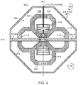
- FIG. 4 illustrates aspects of an integrated circuit 400 (e.g., 300 ), in accordance with an example of this disclosure.
- a tank circuit 304 of the integrated circuit 400 resides on a substrate ( 302 ).
- Tank circuit 304 is surrounded by an electromagnetic (EM) ring 401 .
- the integrated circuit 400 includes a driver 402 which drives components of the tank circuit 304 .
- the EM ring 401 is composed of solid metal and serves to minimize unwanted coupling by circuit 400 components (e.g., tank circuit 304 ) with other circuitry (not shown)
- the tank circuit 304 includes a first inductive loop 306 and a second inductive loop 308 .
- Inductive loop 306 and inductive loop 308 form a first pair 305 of inductive loops.
- Inductive loop 306 comprises an inductor L 1 .
- Inductive loop 308 also comprises an inductor L 2 .
- Inductive loop 306 encloses a capacitive element (C 1 ) 314 and a negative resistive value ( ⁇ R).
- capacitive element C 1 314 is connected to a processor (e.g., 324 ).
- the processor ( 324 ) can cause the capacitance of capacitive element C 1 314 to change.
- Capacitive element C 1 314 is connected in parallel with inductive loop 306 .
- Inductive loop 308 encloses a second capacitive element 316 (C 2 ) and the negative resistive value ( ⁇ R).
- capacitive element C 2 316 is connected to a processor (e.g., 324 ) which can control the capacitance of capacitive element C 2 316 .
- Capacitive element C 2 316 is connected in parallel with inductive loop 308 .
- Circuit 400 also includes a third inductive loop 318 and a fourth inductive loop 319 .
- Inductive loop 318 comprises inductor L 3
- inductive loop 319 comprises inductor L 4 .
- circuit 400 is connected to a switch arrangement (e.g., 320 ).
- Switch arrangement ( 320 ) is controlled by processor ( 324 ) to place the circuit 400 into either of two operating configurations ( 310 , 312 ).
- the circuit 400 includes an oscillation driver 402 that drives the tank circuit 304 at a resonance frequency.
- the resonance frequency is tunable by operation of the processor ( 324 ) on capacitive element C 1 314 , capacitive element C 2 316 , and switch arrangement ( 320 , see FIGS. 3A-3D ).
- the circuit 400 receives input voltage 408 and is connected to local ground 404 .
- the input resonance frequency from driver 402 is tunable as output 406 from the circuit 400 , (making the tank circuit 304 a voltage-controlled oscillator
- the first pair 305 of inductive loops is spaced apart along a first axis 410 and the second pair of inductive loops 315 is spaced apart along a second axis 412 perpendicular to the first axis 410 so as to form a pattern 322 having four-fold symmetry.
- FIG. 5 illustrates a method 500 for operating a tank circuit (e.g., 104 , 304 ), in accordance with an example of this disclosure.
- the method 500 includes receiving 505 a drive signal at a tank circuit (e.g., 104 , 304 ) in a first configuration (e.g., 110 , 310 ).
- the drive signal may come from an oscillation driver (e.g., 202 , 402 ).
- the method 500 also includes driving 507 the tank circuit (e.g., 104 , 304 ) in the first configuration (e.g., 110 , 310 ) based on the drive signal.
- the method 500 also includes placing 509 the tank circuit (e.g., 104 , 304 ) into a second configuration (e.g., 112 , 312 ) using a switch arrangement ( 120 , 320 ).
- driving 507 the tank circuit (e.g., 104 , 304 ) in the first configuration (e.g., 110 , 310 ) comprises driving the loops in the first pair (e.g., 105 , 305 ) in parallel.
- each of the inductive loops (e.g. 106 , 108 ) in the first pair (e.g., 105 ) encloses a corresponding capacitive element (e.g., 114 , 116 ) connected in parallel with that inductive loop (e.g., 105 ).
- the method 500 also includes driving 511 a second pair (e.g., 315 ) of inductive loops in parallel with the first pair (e.g., 305 ) of loops, responsive to placing the tank circuit (e.g., 104 , 304 ) into the second configuration (e.g., 112 , 312 ).
- a second pair e.g., 315
- the tank circuit e.g., 104 , 304
- driving the tank circuit (e.g., 104 , 304 ) in the first configuration (e.g., 110 , 310 ) based on the drive signal comprises causing the inductive loops of the first pair (e.g., 105 , 305 ) to carry currents in opposing directions (see e.g., FIGS. 1B-1C , and FIGS. 3B-3C ).
- method 500 also includes causing—responsive to placing the tank circuit (e.g., 104 , 304 ) into the second configuration (e.g., 112, 312)—the inductive loops of the first pair (e.g., 105 , 305 ) to carry currents in a shared direction (see e.g., FIGS. 1D-1E , and FIGS. 3D-3E ).
- the tank circuit e.g., 104 , 304
- the second configuration e.g., 112, 312
- FIG. 6 illustrates an integrated signal transmitter 600 , in accordance with an example of this disclosure.
- Integrated signal transmitter 600 may be an integrated Wi-Fi signal transmitter.
- Integrated signal transmitter 600 includes a voltage-controlled oscillator (VCO) 602 (e.g., 104 , 304 ).
- VCO 602 produces a signal 603 having a tunable reference frequency.
- VCO 602 produces a signal 603 whose (reference) frequency is tunable across a range of 9.8 GHz to 14.25 GHz.
- VCO 602 produces a signal 603 having a frequency that is tunable across a range of at least 10 GHz to 14.125 GHz.
- VCO 602 may be used to produce signals 603 that are tunable across other ranges in accordance with this disclosure.
- the transmitter 600 also includes a frequency divider (M/D) 604 that converts the reference signal 603 into in-phase carrier signal (I) 606 and quadrature half-frequency carrier signal (Q) 608 , each of which has a frequency which is one half the frequency of reference signal 603 .
- M/D frequency divider
- I in-phase carrier signal
- Q quadrature half-frequency carrier signal
- the transmitter 600 also includes a mixer 610 that produces a transmit signal (RFout) 612 by combining the in-phase carrier signals (I) 606 and the quadrature half-frequency carrier signals 606 with in-phase Wi-Fi modulation signals (I) 614 and quadrature Wi-Fi modulation signals (Q) 616 .
- a mixer 610 that produces a transmit signal (RFout) 612 by combining the in-phase carrier signals (I) 606 and the quadrature half-frequency carrier signals 606 with in-phase Wi-Fi modulation signals (I) 614 and quadrature Wi-Fi modulation signals (Q) 616 .
- an output pin 618 couples the transmit signal (RFout) 612 to an antenna 620 .
- the VCO 602 comprises a configurable tank circuit (e.g. 104 , 304 ) on a substrate (e.g. 102 , 302 ).
- the VCO 602 includes a first pair (e.g., 105 , 305 ) of inductive loops (e.g., 106 , 108 , 306 , 308 ) driven in parallel in each of a first configuration (e.g., 110 , 310 ) and a second configuration (e.g., 112 , 312 ).
- each of the inductive loops in the first pair encloses a corresponding capacitive element (e.g., 114 , 116 , 314 , 316 ) connected in parallel with that inductive loop (e.g., 106 , 108 , 306 , 308 ).
- the VCO 602 also includes a second pair (e.g., 115 , 315 ) of inductive loops which is driven in parallel with the first pair of loops in the second configuration and undriven in the first configuration.
- the VCO 602 also includes a switch arrangement (e.g., 120 , 320 ) that selectively (alternatingly) places the configurable tank circuit (e.g., 104 , 304 ) into either of the first configuration (e.g., 110 , 310 ) or the second configuration (e.g., 112 , 312 ).
- the VCO 602 also includes an oscillation driver (e.g., 202 , 402 ) that drives the configurable tank circuit (e.g., 104 , 304 ) at a tunable resonance frequency.
- FIG. 7 illustrates an integrated signal transmitter 700 , in accordance with an example of this disclosure.
- the integrated signal transmitter 700 can be a Wi-Fi transmitter.
- the integrated signal transmitter 700 includes a VCO 702 , (e.g., 104 , 304 ) producing a reference signal S- 1 having a frequency (a) that is tunable across a range of at least 3.33 GHz to 4.83 GHz.
- Signal S- 1 is output to range expansion circuit 703 .
- range expansion circuit 703 produces a signal 722 based on signal S- 1 having a frequency which is three times greater than the frequency of signal S- 1 .
- VCO 702 may produce a reference signal S- 1 whose frequency (a) is tunable across other ranges.
- the value of signal S- 1 corresponds to the trigonometric function cos(a).
- Signal S- 1 is received by range expansion circuit 703 at polyphase filter (PF 1 ) 706 .
- Polyphase filter PF 1 706 produces a copy of S- 1 (an in-phase reference signal 708 ) and signal S- 2 .
- Signal S- 2 is the same as signal S- 1 except that signal S- 2 is 90 degrees out of phase with signal 5 - 1 , making signal S- 2 a quadrature phase reference signal.
- transmitter 700 also includes a mixer (M 1 ) 710 .
- the mixer M 1 710 combines the reference signal S- 1 with the quadrature phase reference signal S- 2 to produce signal S- 3 having a frequency which is twice that of reference signal S- 1 (a double frequency signal). That is, mixer M 1 710 multiplies cos( ⁇ ) by sin( ⁇ ) to produce signal S- 3 .
- the in-phase double-frequency signal S- 4 and the quadrature phase double-frequency signal S- 5 each have a frequency (2 ⁇ ) which is double the frequency ( ⁇ ) of signal S- 1 .
- the transmitter 700 also includes a mixer arrangement 720 .
- Signals 5 - 1 , S- 2 , S- 4 , and S- 5 are fed to mixer arrangement 720 .
- polyphase filter PF 2 714 enables range expansion circuit 703 to separate wanted tones (sin(3 ⁇ )) and unwanted tones (sin( ⁇ )), which enables mixer arrangement 720 to produce signal S- 8 .
- Mixer arrangement 720 combines S- 1 (in-phase reference signal 708 ) and quadrature phase reference signal S- 2 with in-phase double-frequency signal S- 4 and quadrature phase double-frequency signal to produce signal 722 (S- 8 ) whose frequency is three times that of the reference signal S- 1 (a triple-frequency signal).
- mixer M 2 738 multiplies signal S- 2 (sin( ⁇ )) by signal S- 4 (cos(2 ⁇ )) to produce signal S- 6 . Since cos(2 ⁇ )*sin( ⁇ ) equals 1 ⁇ 2*sin(3 ⁇ ) ⁇ 1 ⁇ 2*sin( ⁇ ), signal S- 6 corresponds to the function 1 ⁇ 2*sin(3 ⁇ )-1 ⁇ 2*sin( ⁇ ).
- Mixer M 3 740 multiplies signal S- 1 (cos( ⁇ )) by signal S- 5 (sin(2 ⁇ )) to produce signal S- 7 . Since cos( ⁇ )*sin(2 ⁇ ) equals 1 ⁇ 2*sin(3 ⁇ ) plus 1 ⁇ 2*sin( ⁇ ), signal S- 7 corresponds to the function 1 ⁇ 2*sin(3 ⁇ )+1 ⁇ 2*sin( ⁇ ).
- Signal S- 6 and signal S- 7 are output to add-circuit 742 .
- Add-circuit 742 adds signal S- 6 (1 ⁇ 2*sin(3 ⁇ ) ⁇ 1 ⁇ 2*sin( ⁇ )) and signal S- 7 (1 ⁇ 2*sin(3 ⁇ )+1 ⁇ 2*sin( ⁇ )) to produce signal S- 8 . Since the equation 1 ⁇ 2*sin(3 ⁇ ) ⁇ 1 ⁇ 2*sin( ⁇ )+1 ⁇ 2*sin(3 ⁇ )+1 ⁇ 2*sin( ⁇ ) reduces to 1 ⁇ 2*sin(3 ⁇ )+1 ⁇ 2*sin(3 ⁇ ), signal S- 8 corresponds to the function sin(3 ⁇ ). The frequency of signal S- 8 (3 ⁇ ) is thus three times that of signal S- 1 ( ⁇ ) from VCO 702 .
- the transmitter 700 also includes output circuit 733 which receives signal S- 8 at frequency divider M/D 724 .
- Frequency divider M/D 724 converts the triple-frequency signal S- 8 ( 722 ) into half-triple-frequency in-phase carrier signals (I) 726 and quadrature carrier signals (Q) 728 .
- the transmitter 700 further includes a modulation mixer M 4 730 that produces transmit signal RFout 732 by combining the half-triple-frequency in-phase carrier signals (I) 726 and quadrature carrier signals (Q) 728 with in-phase Wi-Fi modulation signals 734 and quadrature Wi-Fi modulation signals 736 .
- transmit signal RFout 732 is output to one or more antennas (not shown).
- Examples of this disclosure also include the following enumerated examples:
- An integrated circuit 300 includes a substrate 302 ; a configurable tank circuit 304 on the substrate, the configurable tank circuit including: a first pair 305 of inductive loops 306 , 308 driven in parallel in each of a first configuration 310 and a second configuration 312 , each of the inductive loops 306 , 308 in the first pair 305 enclosing a corresponding capacitive element 314 , 316 connected in parallel with that inductive loop 306 , 308 ; a second pair 315 of inductive loops 316 , 318 driven in parallel with the first pair 305 of loops in the second configuration 312 and undriven in the first configuration 310 ; and a switch arrangement 320 that selectively places the configurable tank circuit 304 into either of the first and second configurations; and an oscillation driver 202 that drives the configurable tank circuit at a tunable resonance frequency.
- each corresponding capacitive element 314 , 116 is an interdigitated capacitor.
- each of the inductive loops in the first pair is an inner loop enclosed within an outer loop, the outer loop being an inductive loop of the second pair.
- each inner loop carries current in a shared direction with its outer loop.
- the oscillation driver includes a voltage-tunable capacitance that enables tuning of the tunable resonance frequency.
- An integrated Wi-Fi signal transmitter that comprises: a voltage-controlled oscillator (VCO) 602 producing a reference frequency 503 that is tunable across a range of at least 10 GHz to 14.125 GHz; a frequency divider 504 that converts the reference frequency 603 into in-phase carrier signals (I) 606 and quadrature half-frequency carrier signals (Q) 608 ; a mixer 610 that produces a transmit signal (RFout) 612 by combining the in-phase carrier signals and the quadrature half-frequency carrier signals with in-phase Wi-Fi modulation signals (I) 614 and quadrature Wi-Fi modulation signals (Q) 616 ; and an output pin 618 that couples the transmit signal (RFout) 612 to an antenna.
- VCO voltage-controlled oscillator
- Q quadrature half-frequency carrier signals
- the VCO includes: a configurable tank circuit on a substrate, the configurable tank circuit including: a first pair of inductive loops driven in parallel in each of a first configuration and a second configuration, each of the inductive loops in the first pair enclosing a corresponding capacitive element connected in parallel with that inductive loop; a second pair of inductive loops driven in parallel with the first pair of loops in the second configuration and undriven in the first configuration; and a switch arrangement that selectively places the configurable tank circuit into either of the first and second configurations; and an oscillation driver that drives the configurable tank circuit at a tunable resonance frequency.
- each of the inductive loops in the first pair is an inner loop enclosed within an outer loop, the outer loop being an inductive loop of the second pair.
- a method of manufacturing an integrated circuit with an on-chip voltage-controlled oscillator comprising: providing a configurable tank circuit on an integrated circuit substrate, the configurable tank circuit including: a first pair of inductive loops driven in parallel in each of a first configuration and a second configuration, each of the inductive loops in the first pair enclosing a corresponding capacitive element connected in parallel with that inductive loop; a second pair of inductive loops driven in parallel with the first pair of loops in the second configuration and undriven in the first configuration; and a switch arrangement that selectively places the configurable tank circuit into either of the first and second configurations; and coupling an oscillation driver to drive the configurable tank circuit at a tunable resonance frequency, the oscillation driver including a voltage-tunable capacitor that enables tuning of the tunable resonance frequency.
- each of the inductive loops in the first pair is an inner loop enclosed within an outer loop, the outer loop being an inductive loop of the second pair.
- An integrated Wi-Fi signal transmitter 700 that comprises: a voltage-controlled oscillator (VCO) 702 producing a reference signal 704 having a reference frequency that is tunable across a range of at least 3.33 GHz to 4.83 GHz; a first filter 706 that derives an in-phase reference signal 708 and a quadrature phase reference signal 709 from the reference signal, the in-phase reference signal and the quadrature phase reference signal having the reference frequency; a first mixer M 1710 that combines the in-phase reference signal 704 with the quadrature phase reference signal 709 to produce a double-frequency signal 712 ; a second filter 714 that derives an in-phase double-frequency signal 716 and a quadrature phase double-frequency signal 718 from the double-frequency signal 712 , the in-phase double-frequency signal and the quadrature phase double-frequency signal each having twice the reference frequency; and a mixer 720 arrangement that combines the reference signal 704 and the quadrature phase reference signal 709 with the in-phase double-frequency signal 7
- the mixer arrangement comprises: a second mixer that combines the in-phase reference signal with the quadrature phase double-frequency signal to produce a first up-converted signal with a positive harmonic; a third mixer that combines the quadrature phase reference signal with the in-phase double-frequency signal to produce a second up-converted signal with a negative harmonic; and an add-circuit that sums the first up-converted signal and the second up-converted signal to produce the triple-frequency signal.
- the mixer arrangement includes a mixer that combines the in-phase reference signal with the quadrature phase double-frequency signal to produce a first up-converted signal.
- the first up-converted reference has a positive harmonic.
- the mixer arrangement also includes a third mixer that combines the quadrature phase reference signal with the in-phase double-frequency signal to produce a second up-converted signal.
- the second up-converted signal is characterized by a negative harmonic.
- the mixer arrangement also includes an add-circuit that sums the first up-converted signal and the second up-converted signal to produce the triple-frequency signal.
Landscapes
- Engineering & Computer Science (AREA)
- Computer Networks & Wireless Communication (AREA)
- Signal Processing (AREA)
- Power Engineering (AREA)
- Inductance-Capacitance Distribution Constants And Capacitance-Resistance Oscillators (AREA)
Abstract
Description
where L12=[L1*L2]/[L1+L2] and C=C1+C2.
where L1234=1/[(1/L1)+(1/L2)+(1/L3)+(1/L4)] and C=C1+C2. In at least one example, when operating in the high frequency mode, the output signal of the
where
where L1234=1/[(1/L1)+(1/L2)+(1/L3)+(1/L4)] and C=C1+C2. Current iL1 is induced in
Claims (22)
Priority Applications (4)
| Application Number | Priority Date | Filing Date | Title |
|---|---|---|---|
| US16/835,052 US10965331B2 (en) | 2019-04-22 | 2020-03-30 | Broad range voltage-controlled oscillator |
| TW109113338A TW202044748A (en) | 2019-04-22 | 2020-04-21 | Broad range voltage-controlled oscillator |
| CN202010317621.8A CN111835287B (en) | 2019-04-22 | 2020-04-21 | Wide range voltage controlled oscillator |
| CN202410031776.3A CN117833829A (en) | 2019-04-22 | 2020-04-21 | Wide Range Voltage Controlled Oscillator |
Applications Claiming Priority (2)
| Application Number | Priority Date | Filing Date | Title |
|---|---|---|---|
| US201962837113P | 2019-04-22 | 2019-04-22 | |
| US16/835,052 US10965331B2 (en) | 2019-04-22 | 2020-03-30 | Broad range voltage-controlled oscillator |
Publications (2)
| Publication Number | Publication Date |
|---|---|
| US20200336160A1 US20200336160A1 (en) | 2020-10-22 |
| US10965331B2 true US10965331B2 (en) | 2021-03-30 |
Family
ID=72832067
Family Applications (1)
| Application Number | Title | Priority Date | Filing Date |
|---|---|---|---|
| US16/835,052 Active US10965331B2 (en) | 2019-04-22 | 2020-03-30 | Broad range voltage-controlled oscillator |
Country Status (3)
| Country | Link |
|---|---|
| US (1) | US10965331B2 (en) |
| CN (2) | CN117833829A (en) |
| TW (1) | TW202044748A (en) |
Families Citing this family (3)
| Publication number | Priority date | Publication date | Assignee | Title |
|---|---|---|---|---|
| US12191342B2 (en) | 2021-02-09 | 2025-01-07 | Mediatek Inc. | Asymmetric 8-shaped inductor and corresponding switched capacitor array |
| US20240038443A1 (en) * | 2022-07-28 | 2024-02-01 | Mediatek Inc. | 8-shaped inductor with ground bar structure |
| US12348188B2 (en) * | 2023-07-26 | 2025-07-01 | Apple Inc. | Feedforward cancellation circuit |
Citations (20)
| Publication number | Priority date | Publication date | Assignee | Title |
|---|---|---|---|---|
| US20050253660A1 (en) * | 2004-05-13 | 2005-11-17 | Bingxue Shi | Quadrature VCO using symmetrical spiral inductors and differential varactors |
| US20090156135A1 (en) * | 2007-12-17 | 2009-06-18 | Renesas Technology Corp. | Transceiver |
| US20090243743A1 (en) * | 2008-03-31 | 2009-10-01 | International Business Machines Corporation | Varactor bank switching based on anti-parallel branch configuration |
| US20120120992A1 (en) * | 2010-11-17 | 2012-05-17 | Qualcomm Incorporated | Lo generation and distribution in a multi-band transceiver |
| US20120169384A1 (en) * | 2011-01-04 | 2012-07-05 | Intel Mobile Communications GmbH | Frequency divider arrangement and method for providing a quadrature output signal |
| US20120256673A1 (en) * | 2010-03-29 | 2012-10-11 | Takeji Fujibayashi | Phase adjustment circuit and phase adjustment method |
| US8742859B2 (en) * | 2011-12-06 | 2014-06-03 | Qualcomm Incorporated | Tunable inductor circuit |
| US20150065068A1 (en) * | 2012-04-03 | 2015-03-05 | Ericsson Modems Sa | Inductor Layout, and a Voltage-Controlled Oscillator (VCO) System |
| US20160118964A1 (en) * | 2014-10-28 | 2016-04-28 | Mediatek Inc. | Frequency tripler and local oscillator generator |
| US20160351309A1 (en) * | 2015-05-27 | 2016-12-01 | Silicon Laboratories Inc. | Comb terminals for planar integrated circuit inductor |
| US20170359024A1 (en) * | 2016-06-14 | 2017-12-14 | National Chi Nan University | Voltage-controlled oscillator |
| US9948313B1 (en) * | 2016-12-19 | 2018-04-17 | Silicon Laboratories Inc. | Magnetically differential loop filter capacitor elements and methods related to same |
| US20180190424A1 (en) * | 2017-01-04 | 2018-07-05 | Silicon Laboratories Inc. | Physical design in magnetic environment |
| US20180294681A1 (en) * | 2015-06-30 | 2018-10-11 | Lg Innotek Co., Ltd. | Multi-mode wireless power transmission method and device for same |
| US20180351559A1 (en) * | 2017-06-01 | 2018-12-06 | Fujitsu Limited | Four-phase oscillator and cdr circuit |
| US20190058441A1 (en) * | 2017-08-18 | 2019-02-21 | Fujitsu Limited | Quadrature oscillation circuit and cdr circuit |
| US20190326856A1 (en) * | 2018-04-19 | 2019-10-24 | Fujitsu Limited | Quadrature oscillator, fsk modulator, and optical module |
| US10483910B2 (en) | 2017-02-02 | 2019-11-19 | Credo Technology Group Limited | Multiport inductors for enhanced signal distribution |
| US20190372576A1 (en) * | 2018-05-29 | 2019-12-05 | Speedlink Technology Inc. | Dual voltage controlled oscillator circuits for a broadband phase locked loop for multi-band millimeter-wave 5g communication |
| US20200098500A1 (en) * | 2018-09-20 | 2020-03-26 | Atmosic Technologies Inc. | Point-symmetric on-chip inductor |
Family Cites Families (6)
| Publication number | Priority date | Publication date | Assignee | Title |
|---|---|---|---|---|
| US6326854B1 (en) * | 1999-09-30 | 2001-12-04 | Nortel Networks Limited | Coaxial resonator and oscillation circuits featuring coaxial resonators |
| EP1583221A1 (en) * | 2004-03-31 | 2005-10-05 | NEC Compound Semiconductor Devices, Ltd. | PLL frequency synthesizer circuit and frequency tuning method thereof |
| WO2007040429A1 (en) * | 2005-10-05 | 2007-04-12 | Telefonaktiebolaget Lm Ericsson (Publ) | Oscillating circuit with tunable filter for minimizing phase noise |
| US8058934B2 (en) * | 2009-06-03 | 2011-11-15 | Qualcomm Incorporated | Apparatus and method for frequency generation |
| US8665033B2 (en) * | 2011-02-18 | 2014-03-04 | Qualcomm Incorporated | Varactorless tunable oscillator |
| US9410823B2 (en) * | 2012-07-13 | 2016-08-09 | Qualcomm Incorporated | Systems, methods, and apparatus for detection of metal objects in a predetermined space |
-
2020
- 2020-03-30 US US16/835,052 patent/US10965331B2/en active Active
- 2020-04-21 CN CN202410031776.3A patent/CN117833829A/en active Pending
- 2020-04-21 CN CN202010317621.8A patent/CN111835287B/en active Active
- 2020-04-21 TW TW109113338A patent/TW202044748A/en unknown
Patent Citations (20)
| Publication number | Priority date | Publication date | Assignee | Title |
|---|---|---|---|---|
| US20050253660A1 (en) * | 2004-05-13 | 2005-11-17 | Bingxue Shi | Quadrature VCO using symmetrical spiral inductors and differential varactors |
| US20090156135A1 (en) * | 2007-12-17 | 2009-06-18 | Renesas Technology Corp. | Transceiver |
| US20090243743A1 (en) * | 2008-03-31 | 2009-10-01 | International Business Machines Corporation | Varactor bank switching based on anti-parallel branch configuration |
| US20120256673A1 (en) * | 2010-03-29 | 2012-10-11 | Takeji Fujibayashi | Phase adjustment circuit and phase adjustment method |
| US20120120992A1 (en) * | 2010-11-17 | 2012-05-17 | Qualcomm Incorporated | Lo generation and distribution in a multi-band transceiver |
| US20120169384A1 (en) * | 2011-01-04 | 2012-07-05 | Intel Mobile Communications GmbH | Frequency divider arrangement and method for providing a quadrature output signal |
| US8742859B2 (en) * | 2011-12-06 | 2014-06-03 | Qualcomm Incorporated | Tunable inductor circuit |
| US20150065068A1 (en) * | 2012-04-03 | 2015-03-05 | Ericsson Modems Sa | Inductor Layout, and a Voltage-Controlled Oscillator (VCO) System |
| US20160118964A1 (en) * | 2014-10-28 | 2016-04-28 | Mediatek Inc. | Frequency tripler and local oscillator generator |
| US20160351309A1 (en) * | 2015-05-27 | 2016-12-01 | Silicon Laboratories Inc. | Comb terminals for planar integrated circuit inductor |
| US20180294681A1 (en) * | 2015-06-30 | 2018-10-11 | Lg Innotek Co., Ltd. | Multi-mode wireless power transmission method and device for same |
| US20170359024A1 (en) * | 2016-06-14 | 2017-12-14 | National Chi Nan University | Voltage-controlled oscillator |
| US9948313B1 (en) * | 2016-12-19 | 2018-04-17 | Silicon Laboratories Inc. | Magnetically differential loop filter capacitor elements and methods related to same |
| US20180190424A1 (en) * | 2017-01-04 | 2018-07-05 | Silicon Laboratories Inc. | Physical design in magnetic environment |
| US10483910B2 (en) | 2017-02-02 | 2019-11-19 | Credo Technology Group Limited | Multiport inductors for enhanced signal distribution |
| US20180351559A1 (en) * | 2017-06-01 | 2018-12-06 | Fujitsu Limited | Four-phase oscillator and cdr circuit |
| US20190058441A1 (en) * | 2017-08-18 | 2019-02-21 | Fujitsu Limited | Quadrature oscillation circuit and cdr circuit |
| US20190326856A1 (en) * | 2018-04-19 | 2019-10-24 | Fujitsu Limited | Quadrature oscillator, fsk modulator, and optical module |
| US20190372576A1 (en) * | 2018-05-29 | 2019-12-05 | Speedlink Technology Inc. | Dual voltage controlled oscillator circuits for a broadband phase locked loop for multi-band millimeter-wave 5g communication |
| US20200098500A1 (en) * | 2018-09-20 | 2020-03-26 | Atmosic Technologies Inc. | Point-symmetric on-chip inductor |
Non-Patent Citations (4)
| Title |
|---|
| "Basics of Electrical Engineering, Series vs Parallel Circuit Configuration," available at: http://www.basicsofelectricalengineering.com/2018/02/series-vs-parallel-circuit-configuration.html, Feb. 13, 2018, 6 pages, printed on Oct. 14, 2020. |
| Pengfei Zhang et al., "A 5-GHz Direct-Conversion CMOS Transceiver," IEEE Journal of Solid-State Circuits, vol. 38, No. 12, Dec. 2003, pp. 2232-2238. |
| Yorgos Palaskas et al., "A 5-GHz 108-Mb/s 2 2 MIMO Transceiver RFIC With Fully Integrated 20.5-dBm P1dB Power Amplifiers in 90-nm CMOS," IEEE Journal of Solid-State Circuits, vol. 41, No. 12, Dec. 2006, pp. 2746-2756. |
| Yuan-Hung Chung et al. "A Dual-Band 802.011 abgn/ac Transceiver with Integrated PA and T/R Switch in a Digital Noise Controlled SoC," IEEE 978-1-4799-8682-8/2015, 8 pages. |
Also Published As
| Publication number | Publication date |
|---|---|
| CN117833829A (en) | 2024-04-05 |
| US20200336160A1 (en) | 2020-10-22 |
| CN111835287B (en) | 2024-01-26 |
| CN111835287A (en) | 2020-10-27 |
| TW202044748A (en) | 2020-12-01 |
Similar Documents
| Publication | Publication Date | Title |
|---|---|---|
| EP1929486B1 (en) | Variable integrated inductor | |
| US10965331B2 (en) | Broad range voltage-controlled oscillator | |
| US8502614B2 (en) | Variable inductor, and oscillator and communication system using the same | |
| US8125282B2 (en) | Dual-band coupled VCO | |
| US11336229B2 (en) | Radio frequency oscillator | |
| US7239209B2 (en) | Serially RC coupled quadrature oscillator | |
| EP2769466B1 (en) | Voltage controlled oscillators having low phase noise | |
| JP4932572B2 (en) | 4-phase voltage controlled oscillator with coupling capacitor | |
| US9143136B2 (en) | Pumped distributed wave oscillator system | |
| US9379663B1 (en) | LC oscillator circuit with wide tuning range | |
| JP2011049975A (en) | Voltage controlled oscillator | |
| US8791765B2 (en) | Force-mode distributed wave oscillator and amplifier systems | |
| US7383033B2 (en) | Differential and quadrature harmonic VCO and methods therefor | |
| JP2008311820A (en) | Voltage controlled oscillator and oscillation control system | |
| CN101194417B (en) | Oscillator circuit and method for controlling oscillation frequency | |
| US9602051B1 (en) | Transforming voltage in a voltage controlled oscillator for wireless sensor devices | |
| US9673755B1 (en) | Controlling a switched capacitor bank in a voltage controlled oscillator for wireless sensor devices | |
| EP1368889B1 (en) | Low power crystal oscillator | |
| US11973465B2 (en) | Oscillator circuit | |
| US7205849B2 (en) | Phase locked loop including an integrator-free loop filter | |
| KR102213682B1 (en) | Voltage controlled oscillator to distribute oscillation signal with transformer | |
| KR101780598B1 (en) | Quadrature voltage controled oscillstor | |
| JP2006005486A (en) | Oscillation circuit and voltage controlled oscillator |
Legal Events
| Date | Code | Title | Description |
|---|---|---|---|
| FEPP | Fee payment procedure |
Free format text: ENTITY STATUS SET TO UNDISCOUNTED (ORIGINAL EVENT CODE: BIG.); ENTITY STATUS OF PATENT OWNER: LARGE ENTITY |
|
| AS | Assignment |
Owner name: SEMICONDUCTOR COMPONENTS INDUSTRIES, LLC, ARIZONA Free format text: ASSIGNMENT OF ASSIGNORS INTEREST;ASSIGNORS:KRISHNASAMY MANIAM, NUNTHA KUMAR;MARGAIRAZ, DIDIER;NEO, BENJAMIN HUAT;SIGNING DATES FROM 20200401 TO 20200421;REEL/FRAME:052457/0981 |
|
| AS | Assignment |
Owner name: DEUTSCHE BANK AG NEW YORK BRANCH, AS COLLATERAL AGENT, NEW YORK Free format text: SECURITY INTEREST;ASSIGNORS:SEMICONDUCTOR COMPONENTS INDUSTRIES, LLC;FAIRCHILD SEMICONDUCTOR CORPORATION;REEL/FRAME:052656/0842 Effective date: 20200505 |
|
| STPP | Information on status: patent application and granting procedure in general |
Free format text: RESPONSE TO NON-FINAL OFFICE ACTION ENTERED AND FORWARDED TO EXAMINER |
|
| STPP | Information on status: patent application and granting procedure in general |
Free format text: PUBLICATIONS -- ISSUE FEE PAYMENT VERIFIED |
|
| STCF | Information on status: patent grant |
Free format text: PATENTED CASE |
|
| AS | Assignment |
Owner name: SEMICONDUCTOR COMPONENTS INDUSTRIES, LLC, ARIZONA Free format text: RELEASE BY SECURED PARTY;ASSIGNOR:DEUTSCHE BANK AG NEW YORK BRANCH;REEL/FRAME:063516/0756 Effective date: 20230501 Owner name: SEMICONDUCTOR COMPONENTS INDUSTRIES, LLC, ARIZONA Free format text: RELEASE OF SECURITY INTEREST;ASSIGNOR:DEUTSCHE BANK AG NEW YORK BRANCH;REEL/FRAME:063516/0756 Effective date: 20230501 |
|
| AS | Assignment |
Owner name: MAXLINEAR, INC., CALIFORNIA Free format text: ASSIGNMENT OF ASSIGNORS INTEREST;ASSIGNOR:SEMICONDUCTOR COMPONENTS INDUSTRIES, LLC;REEL/FRAME:063572/0701 Effective date: 20230502 |
|
| AS | Assignment |
Owner name: FAIRCHILD SEMICONDUCTOR CORPORATION, ARIZONA Free format text: RELEASE OF SECURITY INTEREST IN PATENTS RECORDED AT REEL 052656, FRAME 0842;ASSIGNOR:DEUTSCHE BANK AG NEW YORK BRANCH, AS COLLATERAL AGENT;REEL/FRAME:064080/0149 Effective date: 20230622 Owner name: SEMICONDUCTOR COMPONENTS INDUSTRIES, LLC, ARIZONA Free format text: RELEASE OF SECURITY INTEREST IN PATENTS RECORDED AT REEL 052656, FRAME 0842;ASSIGNOR:DEUTSCHE BANK AG NEW YORK BRANCH, AS COLLATERAL AGENT;REEL/FRAME:064080/0149 Effective date: 20230622 |
|
| MAFP | Maintenance fee payment |
Free format text: PAYMENT OF MAINTENANCE FEE, 4TH YEAR, LARGE ENTITY (ORIGINAL EVENT CODE: M1551); ENTITY STATUS OF PATENT OWNER: LARGE ENTITY Year of fee payment: 4 |