US10916629B2 - Nanosheet-CMOS EPROM device with epitaxial oxide charge storage region - Google Patents

Nanosheet-CMOS EPROM device with epitaxial oxide charge storage region Download PDF

Info

Publication number
US10916629B2
US10916629B2 US16/050,810 US201816050810A US10916629B2 US 10916629 B2 US10916629 B2 US 10916629B2 US 201816050810 A US201816050810 A US 201816050810A US 10916629 B2 US10916629 B2 US 10916629B2
Authority
US
United States
Prior art keywords
nanosheet
oxide
silicon channel
channel material
semiconductor
Prior art date
Legal status (The legal status is an assumption and is not a legal conclusion. Google has not performed a legal analysis and makes no representation as to the accuracy of the status listed.)
Active
Application number
US16/050,810
Other versions
US20200044028A1 (en
Inventor
Alexander Reznicek
Jeng-Bang Yau
Tak H. Ning
Ghavam G. Shahidi
Current Assignee (The listed assignees may be inaccurate. Google has not performed a legal analysis and makes no representation or warranty as to the accuracy of the list.)
International Business Machines Corp
Original Assignee
International Business Machines Corp
Priority date (The priority date is an assumption and is not a legal conclusion. Google has not performed a legal analysis and makes no representation as to the accuracy of the date listed.)
Filing date
Publication date
Application filed by International Business Machines Corp filed Critical International Business Machines Corp
Priority to US16/050,810 priority Critical patent/US10916629B2/en
Assigned to INTERNATIONAL BUSINESS MACHINES CORPORATION reassignment INTERNATIONAL BUSINESS MACHINES CORPORATION ASSIGNMENT OF ASSIGNORS INTEREST (SEE DOCUMENT FOR DETAILS). Assignors: SHAHIDI, GHAVAM G., YAU, JENG-BANG, NING, TAK H., REZNICEK, ALEXANDER
Publication of US20200044028A1 publication Critical patent/US20200044028A1/en
Application granted granted Critical
Publication of US10916629B2 publication Critical patent/US10916629B2/en
Active legal-status Critical Current
Anticipated expiration legal-status Critical

Links

Images

Classifications

    • HELECTRICITY
    • H01ELECTRIC ELEMENTS
    • H01LSEMICONDUCTOR DEVICES NOT COVERED BY CLASS H10
    • H01L29/00Semiconductor devices adapted for rectifying, amplifying, oscillating or switching, or capacitors or resistors with at least one potential-jump barrier or surface barrier, e.g. PN junction depletion layer or carrier concentration layer; Details of semiconductor bodies or of electrodes thereof  ; Multistep manufacturing processes therefor
    • H01L29/02Semiconductor bodies ; Multistep manufacturing processes therefor
    • H01L29/06Semiconductor bodies ; Multistep manufacturing processes therefor characterised by their shape; characterised by the shapes, relative sizes, or dispositions of the semiconductor regions ; characterised by the concentration or distribution of impurities within semiconductor regions
    • H01L29/10Semiconductor bodies ; Multistep manufacturing processes therefor characterised by their shape; characterised by the shapes, relative sizes, or dispositions of the semiconductor regions ; characterised by the concentration or distribution of impurities within semiconductor regions with semiconductor regions connected to an electrode not carrying current to be rectified, amplified or switched and such electrode being part of a semiconductor device which comprises three or more electrodes
    • H01L29/1025Channel region of field-effect devices
    • H01L29/1029Channel region of field-effect devices of field-effect transistors
    • HELECTRICITY
    • H01ELECTRIC ELEMENTS
    • H01LSEMICONDUCTOR DEVICES NOT COVERED BY CLASS H10
    • H01L29/00Semiconductor devices adapted for rectifying, amplifying, oscillating or switching, or capacitors or resistors with at least one potential-jump barrier or surface barrier, e.g. PN junction depletion layer or carrier concentration layer; Details of semiconductor bodies or of electrodes thereof  ; Multistep manufacturing processes therefor
    • H01L29/66Types of semiconductor device ; Multistep manufacturing processes therefor
    • H01L29/66007Multistep manufacturing processes
    • H01L29/66075Multistep manufacturing processes of devices having semiconductor bodies comprising group 14 or group 13/15 materials
    • H01L29/66227Multistep manufacturing processes of devices having semiconductor bodies comprising group 14 or group 13/15 materials the devices being controllable only by the electric current supplied or the electric potential applied, to an electrode which does not carry the current to be rectified, amplified or switched, e.g. three-terminal devices
    • H01L29/66409Unipolar field-effect transistors
    • H01L29/66477Unipolar field-effect transistors with an insulated gate, i.e. MISFET
    • H01L29/66545Unipolar field-effect transistors with an insulated gate, i.e. MISFET using a dummy, i.e. replacement gate in a process wherein at least a part of the final gate is self aligned to the dummy gate
    • HELECTRICITY
    • H01ELECTRIC ELEMENTS
    • H01LSEMICONDUCTOR DEVICES NOT COVERED BY CLASS H10
    • H01L21/00Processes or apparatus adapted for the manufacture or treatment of semiconductor or solid state devices or of parts thereof
    • H01L21/70Manufacture or treatment of devices consisting of a plurality of solid state components formed in or on a common substrate or of parts thereof; Manufacture of integrated circuit devices or of parts thereof
    • H01L21/77Manufacture or treatment of devices consisting of a plurality of solid state components or integrated circuits formed in, or on, a common substrate
    • H01L21/78Manufacture or treatment of devices consisting of a plurality of solid state components or integrated circuits formed in, or on, a common substrate with subsequent division of the substrate into plural individual devices
    • H01L21/82Manufacture or treatment of devices consisting of a plurality of solid state components or integrated circuits formed in, or on, a common substrate with subsequent division of the substrate into plural individual devices to produce devices, e.g. integrated circuits, each consisting of a plurality of components
    • H01L21/822Manufacture or treatment of devices consisting of a plurality of solid state components or integrated circuits formed in, or on, a common substrate with subsequent division of the substrate into plural individual devices to produce devices, e.g. integrated circuits, each consisting of a plurality of components the substrate being a semiconductor, using silicon technology
    • H01L21/8221Three dimensional integrated circuits stacked in different levels
    • HELECTRICITY
    • H01ELECTRIC ELEMENTS
    • H01LSEMICONDUCTOR DEVICES NOT COVERED BY CLASS H10
    • H01L21/00Processes or apparatus adapted for the manufacture or treatment of semiconductor or solid state devices or of parts thereof
    • H01L21/70Manufacture or treatment of devices consisting of a plurality of solid state components formed in or on a common substrate or of parts thereof; Manufacture of integrated circuit devices or of parts thereof
    • H01L21/77Manufacture or treatment of devices consisting of a plurality of solid state components or integrated circuits formed in, or on, a common substrate
    • H01L21/78Manufacture or treatment of devices consisting of a plurality of solid state components or integrated circuits formed in, or on, a common substrate with subsequent division of the substrate into plural individual devices
    • H01L21/82Manufacture or treatment of devices consisting of a plurality of solid state components or integrated circuits formed in, or on, a common substrate with subsequent division of the substrate into plural individual devices to produce devices, e.g. integrated circuits, each consisting of a plurality of components
    • H01L21/822Manufacture or treatment of devices consisting of a plurality of solid state components or integrated circuits formed in, or on, a common substrate with subsequent division of the substrate into plural individual devices to produce devices, e.g. integrated circuits, each consisting of a plurality of components the substrate being a semiconductor, using silicon technology
    • H01L21/8232Field-effect technology
    • H01L21/8234MIS technology, i.e. integration processes of field effect transistors of the conductor-insulator-semiconductor type
    • H01L21/8238Complementary field-effect transistors, e.g. CMOS
    • H01L21/823814Complementary field-effect transistors, e.g. CMOS with a particular manufacturing method of the source or drain structures, e.g. specific source or drain implants or silicided source or drain structures or raised source or drain structures
    • HELECTRICITY
    • H01ELECTRIC ELEMENTS
    • H01LSEMICONDUCTOR DEVICES NOT COVERED BY CLASS H10
    • H01L21/00Processes or apparatus adapted for the manufacture or treatment of semiconductor or solid state devices or of parts thereof
    • H01L21/70Manufacture or treatment of devices consisting of a plurality of solid state components formed in or on a common substrate or of parts thereof; Manufacture of integrated circuit devices or of parts thereof
    • H01L21/77Manufacture or treatment of devices consisting of a plurality of solid state components or integrated circuits formed in, or on, a common substrate
    • H01L21/78Manufacture or treatment of devices consisting of a plurality of solid state components or integrated circuits formed in, or on, a common substrate with subsequent division of the substrate into plural individual devices
    • H01L21/82Manufacture or treatment of devices consisting of a plurality of solid state components or integrated circuits formed in, or on, a common substrate with subsequent division of the substrate into plural individual devices to produce devices, e.g. integrated circuits, each consisting of a plurality of components
    • H01L21/822Manufacture or treatment of devices consisting of a plurality of solid state components or integrated circuits formed in, or on, a common substrate with subsequent division of the substrate into plural individual devices to produce devices, e.g. integrated circuits, each consisting of a plurality of components the substrate being a semiconductor, using silicon technology
    • H01L21/8232Field-effect technology
    • H01L21/8234MIS technology, i.e. integration processes of field effect transistors of the conductor-insulator-semiconductor type
    • H01L21/8238Complementary field-effect transistors, e.g. CMOS
    • H01L21/823821Complementary field-effect transistors, e.g. CMOS with a particular manufacturing method of transistors with a horizontal current flow in a vertical sidewall of a semiconductor body, e.g. FinFET, MuGFET
    • HELECTRICITY
    • H01ELECTRIC ELEMENTS
    • H01LSEMICONDUCTOR DEVICES NOT COVERED BY CLASS H10
    • H01L27/00Devices consisting of a plurality of semiconductor or other solid-state components formed in or on a common substrate
    • H01L27/02Devices consisting of a plurality of semiconductor or other solid-state components formed in or on a common substrate including semiconductor components specially adapted for rectifying, oscillating, amplifying or switching and having at least one potential-jump barrier or surface barrier; including integrated passive circuit elements with at least one potential-jump barrier or surface barrier
    • H01L27/04Devices consisting of a plurality of semiconductor or other solid-state components formed in or on a common substrate including semiconductor components specially adapted for rectifying, oscillating, amplifying or switching and having at least one potential-jump barrier or surface barrier; including integrated passive circuit elements with at least one potential-jump barrier or surface barrier the substrate being a semiconductor body
    • H01L27/06Devices consisting of a plurality of semiconductor or other solid-state components formed in or on a common substrate including semiconductor components specially adapted for rectifying, oscillating, amplifying or switching and having at least one potential-jump barrier or surface barrier; including integrated passive circuit elements with at least one potential-jump barrier or surface barrier the substrate being a semiconductor body including a plurality of individual components in a non-repetitive configuration
    • H01L27/0688Integrated circuits having a three-dimensional layout
    • HELECTRICITY
    • H01ELECTRIC ELEMENTS
    • H01LSEMICONDUCTOR DEVICES NOT COVERED BY CLASS H10
    • H01L27/00Devices consisting of a plurality of semiconductor or other solid-state components formed in or on a common substrate
    • H01L27/02Devices consisting of a plurality of semiconductor or other solid-state components formed in or on a common substrate including semiconductor components specially adapted for rectifying, oscillating, amplifying or switching and having at least one potential-jump barrier or surface barrier; including integrated passive circuit elements with at least one potential-jump barrier or surface barrier
    • H01L27/04Devices consisting of a plurality of semiconductor or other solid-state components formed in or on a common substrate including semiconductor components specially adapted for rectifying, oscillating, amplifying or switching and having at least one potential-jump barrier or surface barrier; including integrated passive circuit elements with at least one potential-jump barrier or surface barrier the substrate being a semiconductor body
    • H01L27/08Devices consisting of a plurality of semiconductor or other solid-state components formed in or on a common substrate including semiconductor components specially adapted for rectifying, oscillating, amplifying or switching and having at least one potential-jump barrier or surface barrier; including integrated passive circuit elements with at least one potential-jump barrier or surface barrier the substrate being a semiconductor body including only semiconductor components of a single kind
    • H01L27/085Devices consisting of a plurality of semiconductor or other solid-state components formed in or on a common substrate including semiconductor components specially adapted for rectifying, oscillating, amplifying or switching and having at least one potential-jump barrier or surface barrier; including integrated passive circuit elements with at least one potential-jump barrier or surface barrier the substrate being a semiconductor body including only semiconductor components of a single kind including field-effect components only
    • H01L27/088Devices consisting of a plurality of semiconductor or other solid-state components formed in or on a common substrate including semiconductor components specially adapted for rectifying, oscillating, amplifying or switching and having at least one potential-jump barrier or surface barrier; including integrated passive circuit elements with at least one potential-jump barrier or surface barrier the substrate being a semiconductor body including only semiconductor components of a single kind including field-effect components only the components being field-effect transistors with insulated gate
    • H01L27/092Devices consisting of a plurality of semiconductor or other solid-state components formed in or on a common substrate including semiconductor components specially adapted for rectifying, oscillating, amplifying or switching and having at least one potential-jump barrier or surface barrier; including integrated passive circuit elements with at least one potential-jump barrier or surface barrier the substrate being a semiconductor body including only semiconductor components of a single kind including field-effect components only the components being field-effect transistors with insulated gate complementary MIS field-effect transistors
    • H01L27/0924Devices consisting of a plurality of semiconductor or other solid-state components formed in or on a common substrate including semiconductor components specially adapted for rectifying, oscillating, amplifying or switching and having at least one potential-jump barrier or surface barrier; including integrated passive circuit elements with at least one potential-jump barrier or surface barrier the substrate being a semiconductor body including only semiconductor components of a single kind including field-effect components only the components being field-effect transistors with insulated gate complementary MIS field-effect transistors including transistors with a horizontal current flow in a vertical sidewall of a semiconductor body, e.g. FinFET, MuGFET
    • H01L27/11568
    • HELECTRICITY
    • H01ELECTRIC ELEMENTS
    • H01LSEMICONDUCTOR DEVICES NOT COVERED BY CLASS H10
    • H01L29/00Semiconductor devices adapted for rectifying, amplifying, oscillating or switching, or capacitors or resistors with at least one potential-jump barrier or surface barrier, e.g. PN junction depletion layer or carrier concentration layer; Details of semiconductor bodies or of electrodes thereof  ; Multistep manufacturing processes therefor
    • H01L29/02Semiconductor bodies ; Multistep manufacturing processes therefor
    • H01L29/06Semiconductor bodies ; Multistep manufacturing processes therefor characterised by their shape; characterised by the shapes, relative sizes, or dispositions of the semiconductor regions ; characterised by the concentration or distribution of impurities within semiconductor regions
    • H01L29/0657Semiconductor bodies ; Multistep manufacturing processes therefor characterised by their shape; characterised by the shapes, relative sizes, or dispositions of the semiconductor regions ; characterised by the concentration or distribution of impurities within semiconductor regions characterised by the shape of the body
    • H01L29/0665Semiconductor bodies ; Multistep manufacturing processes therefor characterised by their shape; characterised by the shapes, relative sizes, or dispositions of the semiconductor regions ; characterised by the concentration or distribution of impurities within semiconductor regions characterised by the shape of the body the shape of the body defining a nanostructure
    • H01L29/0669Nanowires or nanotubes
    • H01L29/0673Nanowires or nanotubes oriented parallel to a substrate
    • HELECTRICITY
    • H01ELECTRIC ELEMENTS
    • H01LSEMICONDUCTOR DEVICES NOT COVERED BY CLASS H10
    • H01L29/00Semiconductor devices adapted for rectifying, amplifying, oscillating or switching, or capacitors or resistors with at least one potential-jump barrier or surface barrier, e.g. PN junction depletion layer or carrier concentration layer; Details of semiconductor bodies or of electrodes thereof  ; Multistep manufacturing processes therefor
    • H01L29/40Electrodes ; Multistep manufacturing processes therefor
    • H01L29/401Multistep manufacturing processes
    • H01L29/4011Multistep manufacturing processes for data storage electrodes
    • H01L29/40117Multistep manufacturing processes for data storage electrodes the electrodes comprising a charge-trapping insulator
    • HELECTRICITY
    • H01ELECTRIC ELEMENTS
    • H01LSEMICONDUCTOR DEVICES NOT COVERED BY CLASS H10
    • H01L29/00Semiconductor devices adapted for rectifying, amplifying, oscillating or switching, or capacitors or resistors with at least one potential-jump barrier or surface barrier, e.g. PN junction depletion layer or carrier concentration layer; Details of semiconductor bodies or of electrodes thereof  ; Multistep manufacturing processes therefor
    • H01L29/66Types of semiconductor device ; Multistep manufacturing processes therefor
    • H01L29/66007Multistep manufacturing processes
    • H01L29/66075Multistep manufacturing processes of devices having semiconductor bodies comprising group 14 or group 13/15 materials
    • H01L29/66227Multistep manufacturing processes of devices having semiconductor bodies comprising group 14 or group 13/15 materials the devices being controllable only by the electric current supplied or the electric potential applied, to an electrode which does not carry the current to be rectified, amplified or switched, e.g. three-terminal devices
    • H01L29/66409Unipolar field-effect transistors
    • H01L29/66477Unipolar field-effect transistors with an insulated gate, i.e. MISFET
    • H01L29/66553Unipolar field-effect transistors with an insulated gate, i.e. MISFET using inside spacers, permanent or not
    • HELECTRICITY
    • H01ELECTRIC ELEMENTS
    • H01LSEMICONDUCTOR DEVICES NOT COVERED BY CLASS H10
    • H01L29/00Semiconductor devices adapted for rectifying, amplifying, oscillating or switching, or capacitors or resistors with at least one potential-jump barrier or surface barrier, e.g. PN junction depletion layer or carrier concentration layer; Details of semiconductor bodies or of electrodes thereof  ; Multistep manufacturing processes therefor
    • H01L29/66Types of semiconductor device ; Multistep manufacturing processes therefor
    • H01L29/68Types of semiconductor device ; Multistep manufacturing processes therefor controllable by only the electric current supplied, or only the electric potential applied, to an electrode which does not carry the current to be rectified, amplified or switched
    • H01L29/76Unipolar devices, e.g. field effect transistors
    • H01L29/772Field effect transistors
    • H01L29/78Field effect transistors with field effect produced by an insulated gate
    • H01L29/792Field effect transistors with field effect produced by an insulated gate with charge trapping gate insulator, e.g. MNOS-memory transistors
    • HELECTRICITY
    • H10SEMICONDUCTOR DEVICES; ELECTRIC SOLID-STATE DEVICES NOT OTHERWISE PROVIDED FOR
    • H10BELECTRONIC MEMORY DEVICES
    • H10B43/00EEPROM devices comprising charge-trapping gate insulators
    • H10B43/20EEPROM devices comprising charge-trapping gate insulators characterised by three-dimensional arrangements, e.g. with cells on different height levels
    • HELECTRICITY
    • H10SEMICONDUCTOR DEVICES; ELECTRIC SOLID-STATE DEVICES NOT OTHERWISE PROVIDED FOR
    • H10BELECTRONIC MEMORY DEVICES
    • H10B43/00EEPROM devices comprising charge-trapping gate insulators
    • H10B43/30EEPROM devices comprising charge-trapping gate insulators characterised by the memory core region
    • HELECTRICITY
    • H01ELECTRIC ELEMENTS
    • H01LSEMICONDUCTOR DEVICES NOT COVERED BY CLASS H10
    • H01L21/00Processes or apparatus adapted for the manufacture or treatment of semiconductor or solid state devices or of parts thereof
    • H01L21/70Manufacture or treatment of devices consisting of a plurality of solid state components formed in or on a common substrate or of parts thereof; Manufacture of integrated circuit devices or of parts thereof
    • H01L21/77Manufacture or treatment of devices consisting of a plurality of solid state components or integrated circuits formed in, or on, a common substrate
    • H01L21/78Manufacture or treatment of devices consisting of a plurality of solid state components or integrated circuits formed in, or on, a common substrate with subsequent division of the substrate into plural individual devices
    • H01L21/82Manufacture or treatment of devices consisting of a plurality of solid state components or integrated circuits formed in, or on, a common substrate with subsequent division of the substrate into plural individual devices to produce devices, e.g. integrated circuits, each consisting of a plurality of components
    • H01L21/822Manufacture or treatment of devices consisting of a plurality of solid state components or integrated circuits formed in, or on, a common substrate with subsequent division of the substrate into plural individual devices to produce devices, e.g. integrated circuits, each consisting of a plurality of components the substrate being a semiconductor, using silicon technology
    • H01L21/8232Field-effect technology
    • H01L21/8234MIS technology, i.e. integration processes of field effect transistors of the conductor-insulator-semiconductor type
    • H01L21/8238Complementary field-effect transistors, e.g. CMOS
    • H01L21/823807Complementary field-effect transistors, e.g. CMOS with a particular manufacturing method of the channel structures, e.g. channel implants, halo or pocket implants, or channel materials
    • HELECTRICITY
    • H01ELECTRIC ELEMENTS
    • H01LSEMICONDUCTOR DEVICES NOT COVERED BY CLASS H10
    • H01L21/00Processes or apparatus adapted for the manufacture or treatment of semiconductor or solid state devices or of parts thereof
    • H01L21/70Manufacture or treatment of devices consisting of a plurality of solid state components formed in or on a common substrate or of parts thereof; Manufacture of integrated circuit devices or of parts thereof
    • H01L21/77Manufacture or treatment of devices consisting of a plurality of solid state components or integrated circuits formed in, or on, a common substrate
    • H01L21/78Manufacture or treatment of devices consisting of a plurality of solid state components or integrated circuits formed in, or on, a common substrate with subsequent division of the substrate into plural individual devices
    • H01L21/82Manufacture or treatment of devices consisting of a plurality of solid state components or integrated circuits formed in, or on, a common substrate with subsequent division of the substrate into plural individual devices to produce devices, e.g. integrated circuits, each consisting of a plurality of components
    • H01L21/822Manufacture or treatment of devices consisting of a plurality of solid state components or integrated circuits formed in, or on, a common substrate with subsequent division of the substrate into plural individual devices to produce devices, e.g. integrated circuits, each consisting of a plurality of components the substrate being a semiconductor, using silicon technology
    • H01L21/8232Field-effect technology
    • H01L21/8234MIS technology, i.e. integration processes of field effect transistors of the conductor-insulator-semiconductor type
    • H01L21/8238Complementary field-effect transistors, e.g. CMOS
    • H01L21/823878Complementary field-effect transistors, e.g. CMOS isolation region manufacturing related aspects, e.g. to avoid interaction of isolation region with adjacent structure
    • HELECTRICITY
    • H01ELECTRIC ELEMENTS
    • H01LSEMICONDUCTOR DEVICES NOT COVERED BY CLASS H10
    • H01L29/00Semiconductor devices adapted for rectifying, amplifying, oscillating or switching, or capacitors or resistors with at least one potential-jump barrier or surface barrier, e.g. PN junction depletion layer or carrier concentration layer; Details of semiconductor bodies or of electrodes thereof  ; Multistep manufacturing processes therefor
    • H01L29/66Types of semiconductor device ; Multistep manufacturing processes therefor
    • H01L29/66007Multistep manufacturing processes
    • H01L29/66075Multistep manufacturing processes of devices having semiconductor bodies comprising group 14 or group 13/15 materials
    • H01L29/66227Multistep manufacturing processes of devices having semiconductor bodies comprising group 14 or group 13/15 materials the devices being controllable only by the electric current supplied or the electric potential applied, to an electrode which does not carry the current to be rectified, amplified or switched, e.g. three-terminal devices
    • H01L29/66409Unipolar field-effect transistors
    • H01L29/66439Unipolar field-effect transistors with a one- or zero-dimensional channel, e.g. quantum wire FET, in-plane gate transistor [IPG], single electron transistor [SET], striped channel transistor, Coulomb blockade transistor

Definitions

  • the present application relates to a semiconductor structure and a method of forming the same. More particularly, the present application relates to a semiconductor structure including a charge storage region that is sandwiched between a pFET nanosheet device and an nFET nanosheet device.
  • nanosheet containing device it is meant that the device contains one or more layers of semiconductor channel material portions having a vertical thickness that is substantially less than its width. Nanosheet formation relies on the selective removal of one semiconductor material relative to another semiconductor material to form suspended nanosheets for gate-all-around devices. There is a need for providing memory devices such as, for example, an electrically programmable read only (EPROM), using nanosheet technology.
  • EPROM electrically programmable read only
  • a semiconductor structure that occupies only one areal device area includes a charge storage region sandwiched between a pFET nanosheet device and an nFET nanosheet device.
  • the charge storage region is an epitaxial oxide nanosheet that is lattice matched to an underlying first silicon channel material nanosheet and an overlying second silicon channel material nanosheet.
  • the semiconductor structure can be used as an EPROM device.
  • the semiconductor structure includes a nanosheet stack comprising an epitaxial oxide nanosheet sandwiched between a first silicon channel material nanosheet and a second silicon channel material nanosheet, and suspended above a semiconductor substrate.
  • a first field effect transistor of a first conductivity type is located beneath the first silicon channel material nanosheet, and a second field effect transistor of a second conductivity type, opposite the first conductivity type, is located above the second silicon channel material nanosheet.
  • a method of forming a semiconductor structure includes forming a nanosheet material stack of, and from bottom to top, a sacrificial semiconductor material nanosheet, a first silicon channel material nanosheet, an epitaxial oxide nanosheet, and a second silicon channel material nanosheet on a surface of a semiconductor substrate and beneath a sacrificial gate structure and a dielectric spacer material layer.
  • the sacrificial semiconductor material nanosheet is recessed to provide a gap between the first silicon channel material nanosheet and the semiconductor substrate.
  • An inner dielectric spacer is then formed in the gap and contacting a sidewall of the recessed sacrificial semiconductor channel material nanosheet.
  • a first source/drain structure is formed on each side of the nanosheet material stack and contacting a sidewall of the first silicon channel material nanosheet, and a second source/drain structure is formed above the first source/drain structure and on each side of the nanosheet material stack.
  • the second source/drain structure contacts a sidewall of the second silicon channel material nanosheet.
  • the sacrificial gate structure and the recessed sacrificial semiconductor material nanosheet are removed to provide a gate cavity containing an upper gate cavity portion located above the second silicon channel material nanosheet, and a lower gate cavity portion located beneath the first silicon channel material nanosheet.
  • a first functional gate structure of a first conductivity type is formed beneath the first silicon channel material nanosheet and in the lower gate cavity portion, and a second functional gate structure of a second conductivity type that is opposite from the first conductivity type is formed above the second silicon channel material nano sheet and in the upper gate cavity portion.
  • FIG. 1 is a cross sectional view of an exemplary semiconductor structure of the present application and during an early stage of fabrication, the exemplary structure including a material stack structure of, and from bottom to top, a sacrificial semiconductor material layer, a first silicon channel material layer, an epitaxial oxide layer, and a second silicon channel material layer located on a surface of a semiconductor substrate.
  • FIG. 2 is a cross sectional view of the exemplary semiconductor structure of FIG. 1 after forming a sacrificial gate structure and a dielectric spacer material layer on a surface of the material stack structure.
  • FIG. 3 is a cross sectional view of the exemplary semiconductor structure of FIG. 2 after removing physically exposed portions of the material stack structure that are not protected by sacrificial gate structure and the dielectric spacer material layer to provide a nanosheet material stack of, and from bottom to top, a sacrificial semiconductor material nanosheet, a first silicon channel material nanosheet, an epitaxial oxide nanosheet, and a second silicon channel material nanosheet located beneath the sacrificial gate structure and the dielectric spacer material layer.
  • FIG. 4 is a cross sectional view of the exemplary semiconductor structure of FIG. 3 after recessing the sacrificial semiconductor material nanosheet and forming an inner dielectric spacer on exposed sidewalls of the recessed sacrificial semiconductor material nanosheet.
  • FIG. 5 is a cross sectional view of the exemplary semiconductor structure of FIG. 4 after forming a first source/drain structure on each side of the nanosheet material stack.
  • FIG. 6 is a cross sectional view of the exemplary semiconductor structure of FIG. 5 after forming a dielectric material layer on the first source/drain structure, forming a second source/drain structure on dielectric material layer, and forming an interlayer dielectric (ILD) material layer of the second source/drain structure.
  • ILD interlayer dielectric
  • FIG. 7 is a cross sectional view of the exemplary semiconductor structure of FIG. 6 after removing the sacrificial gate structure and the recessed sacrificial semiconductor material nanosheet.
  • FIG. 8 is a cross sectional view of the exemplary semiconductor structure of FIG. 7 after forming a first functional gate structure of a first conductivity type beneath the first silicon channel material nanosheet and in an area previously including the recessed sacrificial semiconductor material nanosheet.
  • FIG. 9 is a cross sectional view of the exemplary semiconductor structure of FIG. 8 after forming a second functional gate structure of a second conductivity type that is opposite from the first conductivity type above the second silicon channel material nanosheet and in an area previously including the sacrificial gate structure.
  • FIG. 10 is a cross sectional view of the exemplary semiconductor structure of FIG. 9 after forming contact structures.
  • FIG. 11 is a basic circuit schematic of the exemplary structure of the present application.
  • FIG. 12 is a circuit schematic when the exemplary structure of the present application operates as a CMOS inverter.
  • FIG. 13 is a circuit schematic showing a 3 ⁇ 3 CMOS EPROM array including the exemplary structure of the present application.
  • FIG. 1 there is illustrated an exemplary semiconductor structure of the present application and during an early stage of fabrication, the exemplary structure including a material stack structure of, and from bottom to top, a sacrificial semiconductor material layer 12 , a first silicon channel material layer 14 , an epitaxial oxide layer 16 , and a second silicon channel material layer 18 located on a surface of a semiconductor substrate 10 .
  • the first silicon channel material layer 14 , the epitaxial oxide layer 16 , and the second silicon channel material layer 18 of the material stack structure are lattice matched.
  • the semiconductor substrate 10 that can be employed in the present application includes at least one semiconductor material that has semiconducting properties.
  • semiconductor materials that can be used as the semiconductor substrate 10 include, for example, silicon (Si), a silicon germanium (SiGe) alloy, a silicon germanium carbide (SiGeC) alloy, germanium (Ge), III/V compound semiconductors or II/VI compound semiconductors.
  • the semiconductor substrate 10 is a bulk semiconductor substrate.
  • the term “bulk semiconductor substrate” denotes a substrate that is composed entirely of one or more semiconductor materials. In one example, the bulk semiconductor substrate is composed entirely of Si.
  • the semiconductor substrate 10 is composed of a semiconductor-on-insulator (SOI) substrate.
  • SOI substrate typically includes a handle substrate, an insulator layer and a topmost semiconductor material layer.
  • the handle substrate of the SOI substrate may include a semiconductor material, as described above.
  • the handle substrate may be omitted, or the handle substrate may be composed of a conductive material and/or an insulator material.
  • the insulator layer of the SOI substrate may include a crystalline or non-crystalline dielectric material.
  • the insulator layer of the SOI substrate may be composed of silicon dioxide and/or boron nitride.
  • the topmost semiconductor layer of the SOI substrate is composed of a semiconductor material, as defined above.
  • the material stack structure ( 12 , 14 , 16 , 18 ), as defined above, is then formed on the semiconductor substrate 10 .
  • the material stack structure includes a sacrificial semiconductor material layer 12 , a first silicon channel material layer 14 , an epitaxial oxide layer 16 , and a second silicon channel material layer 18 stacked one atop the other.
  • the sacrificial semiconductor material layer 12 is composed of a semiconductor material which differs in composition from at least an upper portion of the semiconductor substrate 10 an is other than silicon.
  • the sacrificial semiconductor material layer 12 is composed of a silicon germanium alloy.
  • the sacrificial semiconductor material layer 12 can be formed utilizing an epitaxial growth (or deposition process) as defined in greater detail herein below.
  • the first and second silicon channel material layers 14 and 18 have a different etch rate than the sacrificial semiconductor material layer 12 .
  • the first and second silicon channel material layers 14 and 18 can be formed utilizing an epitaxial growth (or deposition process) as defined in greater detail herein below.
  • the epitaxial oxide layer 16 which is sandwiched between the first silicon channel material layer 14 and the second silicon channel material layer 18 , may be selected to have a lattice dimension substantially similar (i.e., ⁇ 5%) to the lattice dimension of the first and second silicon channel material layers ( 14 , 16 ), thus the epitaxial oxide layer 16 is said to be lattice matched to the first and second silicon channel material layers ( 14 , 18 ).
  • the epitaxial oxide layer 16 is epitaxially deposited, as defined below.
  • Examples of epitaxial oxides that are suitable for use as the epitaxial oxide layer 16 may include binary oxides, such as, e.g., lanthanum (II) oxide (La 2 O 3 ) gadolinium(III)-oxide (Gd 2 O 3 ), dysprosium(III)-oxide (Dy 2 O 3 ), holmium(III) oxide (Ho 2 O 3 ), erbium (III) oxide (Er 2 O 3 ), thulium (III) oxide (Tm 2 O 3 ), lutetium(III) oxide (Lu 2 O 3 ) or cerium (IV) oxide (CeO 2 ), ternary oxides including a rare earth metal, such as e.g., Gd, Er, Nd, La and Y forming oxides such as, e.g., lanthanum-yttrium oxide ((La x Y 1-x ) 2 O 3 ), gadolinium-erbium oxide ((Gd x Er 1-x )
  • the thickness of the epitaxial oxide layer 16 can be determined by satisfying the requirement of negligible loss of stored charge by tunneling into the first and second silicon channel material layers 14 and 18 .
  • the tunneling between a silicon channel material layer and the epitaxial oxide layer 16 can be described by the Fowler-Nordheim model. According to this model, and to keep the tunneling current below a desired level, e.g., 1E ⁇ 8 Amperes/cm 2 , the epitaxial oxide field must be lower than about 6 MV/cm.
  • the thickness of the epitaxial oxide layer 16 is from 10 nm to 500 nm. In some embodiments, the thickness of the epitaxial oxide layer 16 is from 10 nm to 100 nm, while in other embodiments the thickness of the epitaxial oxide layer 16 is from 10 nm to 50 nm.
  • Material stack structure ( 12 , 14 , 16 , 18 ) can be formed by sequential epitaxial growth of the sacrificial semiconductor material layer 12 , the first silicon channel material layer 14 , the epitaxial oxide layer 16 , and the second silicon channel material layer 18 . Following epitaxial growth of the second silicon channel material layer 18 , a patterning process may be used to provide the material stack structure ( 12 , 14 , 16 , 18 ) shown in FIG. 1 . Patterning may be performed by lithography and etching or any other patterning method known to those skilled in the art including, for example, a sidewall-image transfer (SIT) process.
  • SIT sidewall-image transfer
  • epitaxially growing and/or depositing and “epitaxially grown and/or deposited” mean the growth of a material (e.g., semiconductor material or epitaxial oxide) on a growth surface of another material, in which the material being grown has the same crystalline characteristics as the material of the growth surface.
  • a material e.g., semiconductor material or epitaxial oxide
  • the chemical reactants provided by the source gases are controlled and the system parameters are set so that the depositing atoms arrive at the growth surface of a material with sufficient energy to move around on the growth surface and orient themselves to the crystal arrangement of the atoms of the growth surface. Therefore, an epitaxial material has the same crystalline characteristics as the growth on surface on which it is formed.
  • Examples of various epitaxial growth process apparatuses that can be employed in the present application include, e.g., rapid thermal chemical vapor deposition (RTCVD), low-energy plasma deposition (LEPD), ultra-high vacuum chemical vapor deposition (UHVCVD), atmospheric pressure chemical vapor deposition (APCVD) and molecular beam epitaxy (MBE).
  • RTCVD rapid thermal chemical vapor deposition
  • LEPD low-energy plasma deposition
  • UHVCVD ultra-high vacuum chemical vapor deposition
  • APCVD atmospheric pressure chemical vapor deposition
  • MBE molecular beam epitaxy
  • the temperature for epitaxial deposition typically ranges from 550° C. to 900° C. Although higher temperature typically results in faster deposition, the faster deposition may result in crystal defects and film cracking.
  • the epitaxial growth of the various material layers can be performed utilizing any well known precursor gas or gas mixture.
  • Carrier gases like hydrogen, nitrogen, helium and argon can be used.
  • material stack structure denotes a continuous structure including a pair of vertical sidewalls that are parallel to each other.
  • a surface is “vertical” if there exists a vertical plane from which the surface does not deviate by more than three times the root mean square roughness of the surface.
  • Each layer within the material stack structure i.e., the sacrificial semiconductor material layer 12 , the first silicon channel material layer 14 , the epitaxial oxide layer 16 and the second silicon channel material layer 18 ) may have a thickness from 5 nm to 12 nm. The thickness of each layer within the material stack structure may be the same or different.
  • FIG. 2 there is illustrated the exemplary semiconductor structure of FIG. 1 after forming a sacrificial gate structure 20 and a dielectric spacer material layer 22 on a surface of the material stack structure ( 12 , 14 , 16 , 18 ).
  • the sacrificial gate structure 20 is located on a first side and a second side of the material stack structure, and spans across a topmost surface of a portion of the material stack structure.
  • the sacrificial gate stack 20 thus straddles over a portion of the material stack structure.
  • a dielectric spacer material layer 22 is present on the exposed surfaces of the sacrificial gate structure 20 .
  • the sacrificial gate structure 20 may include a single sacrificial material or a stack of two or more sacrificial materials (i.e., the sacrificial gate structure 20 includes at least one sacrificial material).
  • the at least one sacrificial material comprises, from bottom to top, a sacrificial gate dielectric material, a sacrificial gate material and a sacrificial dielectric cap.
  • the sacrificial gate dielectric material and/or the sacrificial dielectric cap can be omitted and only a sacrificial gate material is formed.
  • the at least one sacrificial material can be formed by forming a blanket layer (or layers) of a material (or various materials) and then patterning the material (or various materials) by lithography and an etch.
  • the at least one sacrificial material can be formed by first depositing a blanket layer of a sacrificial gate dielectric material.
  • the sacrificial gate dielectric material can be an oxide, nitride, and/or oxynitride.
  • the sacrificial gate dielectric material can be a high k material having a dielectric constant greater than silicon dioxide.
  • a multilayered dielectric structure comprising different dielectric materials, e.g., silicon dioxide, and a high k dielectric can be formed and used as the sacrificial gate dielectric material.
  • the sacrificial gate dielectric material can be formed by any deposition technique including, for example, chemical vapor deposition (CVD), plasma enhanced chemical vapor deposition (PECVD), physical vapor deposition (PVD), sputtering, or atomic layer deposition.
  • a blanket layer of a sacrificial gate material can be formed on the blanket layer of sacrificial gate dielectric material.
  • the sacrificial gate material can include any material including, for example, polysilicon, amorphous silicon, an elemental metal (e.g., tungsten, titanium, tantalum, aluminum, nickel, ruthenium, palladium and platinum), an alloy of at least two elemental metals or multilayered combinations thereof.
  • the sacrificial gate material can be formed utilizing a deposition process including, for example, chemical vapor deposition (CVD), plasma enhanced chemical vapor deposition (PECVD), physical vapor deposition (PVD), sputtering, atomic layer deposition (ALD) or other like deposition processes.
  • CVD chemical vapor deposition
  • PECVD plasma enhanced chemical vapor deposition
  • PVD physical vapor deposition
  • ALD atomic layer deposition
  • a blanket layer of a sacrificial gate cap material can be formed.
  • the sacrificial gate cap material may include a hard mask material such as, for example, silicon dioxide and/or silicon nitride.
  • the sacrificial gate cap material can be formed by any suitable deposition process such as, for example, chemical vapor deposition or plasma enhanced chemical vapor deposition.
  • lithography and etching can be used to pattern the sacrificial material stack (or any subset of the sacrificial materials) and to provide the sacrificial gate structure 20 .
  • the dielectric spacer material layer 22 can be formed by deposition of a dielectric spacer material and then etching the dielectric spacer material.
  • a dielectric spacer material that may be employed in the present application is silicon nitride.
  • the deposition process that can be employed in providing the dielectric spacer material includes, for example, chemical vapor deposition (CVD), plasma enhanced chemical vapor deposition (PECVD), or physical vapor deposition (PVD).
  • the etch used to etch the deposited dielectric spacer material may comprise a dry etching process such as, for example, reactive ion etching.
  • FIG. 3 there is illustrated the exemplary semiconductor structure of FIG. 2 after removing physically exposed portions of the material stack structure ( 12 , 14 , 16 , 18 ) that are not protected by sacrificial gate structure 20 and the dielectric spacer material layer 22 to provide a nanosheet material stack of, and from bottom to top, a sacrificial semiconductor material nanosheet 12 NS, a first silicon channel material nanosheet 14 NS, an epitaxial oxide nanosheet 16 NS, and a second silicon channel material nanosheet 18 NS located beneath the sacrificial gate structure 20 and the dielectric spacer material layer 22 .
  • the sacrificial semiconductor material nanosheet 12 NS, the first silicon channel material nanosheet 14 NS, the epitaxial oxide nanosheet 16 NS, and the second silicon channel material nanosheet 18 NS represent non-removed material layer portions of the material stack structure ( 12 , 14 , 16 , 18 ).
  • the removal of the physically exposed portions of the material stack structure ( 12 , 14 , 16 , 18 ) not covered by the sacrificial gate structure 20 and the dielectric spacer material layer 22 can be performed utilizing an anisotropic etching process such as, for example, reactive ion etching (RIE).
  • RIE reactive ion etching
  • a portion of the material stack structure ( 12 , 14 , 16 , 18 ) remains beneath the sacrificial gate structure 20 and the dielectric spacer material layer 22 .
  • the remaining portion of the material stack structure ( 12 , 14 , 16 , 18 ) that is presented beneath the sacrificial gate structure 20 and the dielectric spacer material layer 22 can be referred to as a nanosheet material stack.
  • the nanosheet material stack structure includes a sacrificial semiconductor material nanosheet 12 NS, a first silicon channel material nanosheet 14 NS, an epitaxial oxide nanosheet 16 NS, and a second silicon channel material nanosheet 18 NS.
  • Each nanosheet i.e., the sacrificial semiconductor material nanosheet 12 NS, the first silicon channel material nanosheet 14 NS, the epitaxial oxide nanosheet 16 NS, and the second silicon channel material nanosheet 18 NS, that constitutes the nanosheet material stack has a thickness as mentioned above for the individual layers of the material stack, and a width from 30 nm to 200 nm.
  • the sidewalls of the nanosheets i.e., the sacrificial semiconductor material nanosheet 12 NS, the first silicon channel material nanosheet 14 NS, the epitaxial oxide nanosheet 16 NS, and the second silicon channel material nanosheet 18 NS
  • the sidewalls of the nanosheets are vertically aligned to each other as well as to an outmost sidewall of the dielectric spacer material layer 22 .
  • FIG. 4 there is illustrated the exemplary semiconductor structure of FIG. 3 after recessing the sacrificial semiconductor material nanosheet 12 NS and forming an inner dielectric spacer 24 S on exposed sidewalls of the recessed sacrificial semiconductor material nanosheet 12 R.
  • the recessed sacrificial semiconductor material nanosheet is designated as element 12 R in the drawings of the present application.
  • the recessed sacrificial semiconductor material nanosheet 12 R has a width that is less than the original width of the sacrificial semiconductor material nanosheet 12 NS.
  • the recessing of the sacrificial semiconductor material nanosheet 12 NS provides a gap (not specifically shown) between the first silicon channel material nanosheet 14 NS and the semiconductor substrate 10 .
  • the recessing of the sacrificial semiconductor material nanosheet 12 NS may be performed utilizing a lateral etching process that is selective in removing physically exposed end portions of the sacrificial semiconductor material nanosheet 12 NS relative to the first and second silicon channel material nanosheet ( 14 NS, 18 NS), and the epitaxial oxide nanosheet 16 NS.
  • the inner dielectric spacer 24 S is formed in the gap that is formed by the recessing of the sacrificial semiconductor material nanosheet 12 NS.
  • the inner dielectric spacer 24 S is formed by deposition of a dielectric spacer material and etching the deposited dielectric spacer material.
  • the dielectric spacer material that provides the inner dielectric spacer 24 S may be the same as, or different from, the dielectric spacer material that provides the dielectric spacer material layer 22 .
  • the inner dielectric spacer 24 S has an innermost sidewall that directly contacts a sidewall of the recessed sacrificial semiconductor material nanosheet, and an outermost sidewall that is vertically aligned with the sidewalls of the first and second silicon channel material nanosheets ( 14 NS, 18 NS), the epitaxial oxide nanosheet 16 NS, and the dielectric spacer material layer 22 .
  • FIG. 5 there is illustrated the exemplary semiconductor structure of FIG. 4 after forming a first source/drain structure 26 S on each side of the nanosheet material stack and from a physically exposed sidewall of the first silicon channel material nanosheet 14 NS.
  • the first source/drain structure 26 S has a topmost surface that is located between the topmost surface and the bottommost surface of the epitaxial oxide nanosheet 16 NS.
  • the first source/drain structure 26 S has a bottommost surface that may directly contact the semiconductor substrate 10 .
  • the first source/drain structure 26 S can be formed by epitaxial growth of a semiconductor material on physically exposed sidewalls of the first silicon channel material nanosheet 14 NS and, optionally, upwards from the semiconductor substrate 10 .
  • a recess etch may follow the epitaxial growth of the semiconductor material that provides the first source/drain structure 26 S.
  • the deposited semiconductor material that provides the first source/drain structure 26 S may have a faceted upper surface.
  • the first source/drain structure 26 S includes a semiconductor material and a dopant.
  • the semiconductor material that provides first source/drain structure 26 S can be selected from one of the semiconductor materials mentioned above for the semiconductor substrate 10 .
  • the semiconductor material that provides first source/drain structure 26 S may be composed of silicon.
  • the dopant that is present in first source/drain structure 26 S can be either a p-type dopant or an n-type dopant.
  • p-type refers to the addition of impurities to an intrinsic semiconductor that creates deficiencies of valence electrons.
  • examples of p-type dopants, i.e., impurities include, but are not limited to, boron, aluminum, gallium and indium.
  • N-type refers to the addition of impurities that contributes free electrons to an intrinsic semiconductor.
  • examples of n-type dopants, i.e., impurities include, but are not limited to, antimony, arsenic and phosphorous.
  • the first source/drain structure 26 S may have a dopant concentration of from 4 ⁇ 10 20 atoms/cm 3 to 3 ⁇ 10 21 atoms/cm 3 .
  • the first source/drain structure 26 S is composed of phosphorous doped silicon.
  • the first silicon channel material nanosheet 14 NS will be used as the channel of an n-type FET (or nFET for short).
  • the dopant that can be present in the first source/drain structure 26 S can be introduced into the precursor gas that provides the first source/drain structure 26 S.
  • the dopant can be introduced into an intrinsic semiconductor layer by utilizing one of ion implantation or gas phase doping.
  • FIG. 6 there is illustrated the exemplary semiconductor structure of FIG. 5 after forming a dielectric material layer 28 on the first source/drain structure 26 S, forming a second source/drain structure 30 S on dielectric material layer 28 , and forming an interlayer dielectric (ILD) material layer 32 of the second source/drain structure 30 S.
  • ILD interlayer dielectric
  • the dielectric material layer 28 may include any dielectric material such as, for example, silicon dioxide, that can be formed by a thermal oxidation process or by a deposition process such as, for example, chemical vapor deposition (CVD) or plasma enhanced chemical vapor deposition. A recess etch may follow the thermal oxidation or deposition process.
  • the dielectric material layer 28 has a bottommost surface that is in direct physical contact with a topmost surface of the first source/drain structure, a sidewall surface that contacts the epitaxial oxide nanosheet 16 NS, and a topmost surface that is located beneath, or coplanar with, the bottommost surface of the second silicon channel material nanosheet 18 NS.
  • the second source/drain structure 30 S is formed utilizing an epitaxial growth process.
  • the second source/drain structure 30 S is formed on, and outward from, the physically exposed sidewall of the second silicon channel material nanosheet 18 NS.
  • the second source/drain structure 30 S may have a faceted upper surface.
  • the second source/drain structure 30 S includes a semiconductor material and a dopant.
  • the semiconductor material that provides second source/drain structure 30 S can be selected from one of the semiconductor materials mentioned above for the semiconductor substrate 10 .
  • the semiconductor material that provides second source/drain structure 30 S may be composed of a silicon germanium alloy.
  • the dopant that is present in second source/drain structure 30 S can be either a p-type dopant or an n-type dopant provided that it has a different conductivity than the dopant that is present in the first source/drain structure 26 S.
  • the second source/drain structure 30 S may have a dopant concentration of from 4 ⁇ 10 20 atoms/cm 3 to 3 ⁇ 10 21 atoms/cm 3 .
  • the second source/drain structure 30 S is composed of a boron doped silicon germanium alloy.
  • the second silicon channel material nanosheet 18 NS will be used as the channel of a p-type FET (or pFET for short).
  • the dopant that can be present in the second source/drain structure 30 S can be introduced into the precursor gas that provides the second source/drain structure 30 S.
  • the dopant can be introduced into an intrinsic semiconductor layer by utilizing one of ion implantation or gas phase doping.
  • the interlayer dielectric (ILD) material layer 32 may be composed of silicon dioxide, undoped silicate glass (USG), fluorosilicate glass (FSG), borophosphosilicate glass (BPSG), a spin-on low-k dielectric layer, a chemical vapor deposition (CVD) low-k dielectric layer or any combination thereof.
  • low-k denotes a dielectric material that has a dielectric constant of less than silicon dioxide.
  • a self-planarizing material such as a spin-on glass (SOG) or a spin-on low-k dielectric material such as SiLKTM can be used as ILD material layer 32 .
  • the use of a self-planarizing dielectric material as the ILD material layer 32 may avoid the need to perform a subsequent planarizing step.
  • the ILD material layer 32 can be formed utilizing a deposition process including, for example, chemical vapor deposition (CVD), plasma enhanced chemical vapor deposition (PECVD), evaporation or spin-on coating.
  • CVD chemical vapor deposition
  • PECVD plasma enhanced chemical vapor deposition
  • evaporation or spin-on coating evaporation or spin-on coating.
  • a planarization process or an etch back process follows the deposition of the dielectric material that provides the ILD material layer 32 .
  • the ILD material layer 32 has a topmost surface that is coplanar with a topmost surface of the dielectric spacer material layer 22 .
  • FIG. 7 there is illustrated the exemplary semiconductor structure of FIG. 6 after removing the sacrificial gate structure 20 and the recessed sacrificial semiconductor material nanosheet 12 R to provide a gate cavity having an upper gate cavity portion 34 and a lower gate cavity portion 36 .
  • a horizontal portion of dielectric spacer material layer 22 is removed from atop the sacrificial gate structure 20 to provide topmost an inner gate spacer 22 S.
  • the removal of the horizontal portion of the dielectric spacer material layer 22 and the sacrificial gate structure 20 can be performed utilizing one or more anisotropic etching processes.
  • the recessed sacrificial semiconductor material nanosheet 12 R can be removed by utilizing an etching process that is selective in removing the recessed sacrificial semiconductor material nanosheet 12 R. After removing the recessed sacrificial semiconductor material nanosheet, the first silicon channel material nanosheet is suspended above the semiconductor substrate 10 .
  • the first functional gate structure is a p-type FET.
  • functional gate structure it is meant a permanent gate structure used to control output current (i.e., flow of carriers in the channel) of a semiconducting device through electrical or magnetic fields.
  • the first functional gate structure ( 38 , 40 ) may include a first gate dielectric portion 38 and a first gate conductor portion 40 .
  • the first gate dielectric portion 38 may include a gate dielectric material.
  • the gate dielectric material that provides the first gate dielectric portion 38 can be an oxide, nitride, and/or oxynitride.
  • the gate dielectric material that provides the first gate dielectric portion 38 can be a high-k material having a dielectric constant greater than silicon dioxide.
  • Exemplary high-k dielectrics include, but are not limited to, HfO 2 , ZrO 2 , La 2 O 3 , Al 2 O 3 , TiO 2 , SrTiO 3 , LaAlO 3 , Y 2 O 3 , HfO x N y , ZrO x N y , La 2 O x N y , Al 2 O x N y , TiO x N y , SrTiO x N y , LaAlO x N y , Y 2 O x N y , SiON, SiN x , a silicate thereof, and an alloy thereof.
  • Each value of x is independently from 0.5 to 3 and each value of y is independently from 0 to 2.
  • a multilayered gate dielectric structure comprising different gate dielectric materials, e.g., silicon dioxide, and a high-k gate dielectric, can be formed and used as the first gate dielectric portion 38 .
  • the gate dielectric material used in providing the first gate dielectric portion 38 can be formed by any deposition process including, for example, chemical vapor deposition (CVD), plasma enhanced chemical vapor deposition (PECVD), physical vapor deposition (PVD), sputtering, or atomic layer deposition.
  • the gate dielectric material used in providing the first gate dielectric portion 38 can have a thickness in a range from 1 nm to 10 nm. Other thicknesses that are lesser than, or greater than, the aforementioned thickness range can also be employed for the gate dielectric material that may provide the first gate dielectric portion 38 .
  • the first gate conductor portion 40 can include a gate conductor material.
  • the gate conductor material used in providing the first gate conductor portion 40 can include any conductive material including, for example, doped polysilicon, an elemental metal (e.g., tungsten, titanium, tantalum, aluminum, nickel, ruthenium, palladium and platinum), an alloy of at least two elemental metals, an elemental metal nitride (e.g., tungsten nitride, aluminum nitride, and titanium nitride), an elemental metal silicide (e.g., tungsten silicide, nickel silicide, and titanium silicide) or multilayered combinations thereof.
  • the gate conductor portion 34 may comprise an nFET gate metal.
  • the first gate conductor portion 40 may comprise a pFET gate metal.
  • the gate conductor material used in providing the first gate conductor portion 40 can be formed utilizing a deposition process including, for example, chemical vapor deposition (CVD), plasma enhanced chemical vapor deposition (PECVD), physical vapor deposition (PVD), sputtering, atomic layer deposition (ALD) or other like deposition processes.
  • CVD chemical vapor deposition
  • PECVD plasma enhanced chemical vapor deposition
  • PVD physical vapor deposition
  • ALD atomic layer deposition
  • the gate conductor material used in providing the first gate conductor portion 40 can have a thickness from 50 nm to 200 nm. Other thicknesses that are lesser than, or greater than, the aforementioned thickness range can also be employed for the gate conductor material used in providing the first gate conductor portion 40 .
  • the first functional gate structure ( 38 , 40 ) can be formed by providing a functional gate material stack of the gate dielectric material, and the gate conductor material. A planarization process may follow the formation of the functional gate material stack, and a recess etch may be used to remove the first functional gate structure ( 38 , 40 ) from the upper gate cavity portion 34 .
  • FIG. 9 there is illustrated the exemplary semiconductor structure of FIG. 8 after forming a second functional gate structure ( 42 , 44 ) of a second conductivity type that is opposite from the first conductivity type above the second silicon channel material nanosheet 18 NS and in an area previously including the sacrificial gate structure 20 (i.e., the upper gate cavity portion 34 ).
  • the second functional gate structure ( 42 , 44 ) may include a second gate dielectric portion 42 and a second gate conductor portion 44 .
  • the second gate dielectric portion 42 may include one of the gate dielectric materials mentioned above for the first gate dielectric portion 38 . In one embodiment, the second gate dielectric portion 42 may include a same gate dielectric material as the first gate dielectric portion 38 . In another embodiment, the second gate dielectric portion 42 may include a different gate dielectric material than the first gate dielectric portion 38 . The second gate conductor portion 44 typically includes a different gate conductor material than the first gate conductor portion 40 .
  • the second functional gate structure ( 42 , 44 ) can be formed by deposition of the gate dielectric material and the gate conductor material, and then planarizing the material stack of the deposited gate dielectric material and the gate conductor material such that a second functional gate structure ( 42 , 44 ) has a topmost surface that is coplanar with a topmost surface of the topmost inner gate spacers 22 S and the ILD material layer 32 .
  • FIG. 9 illustrates a semiconductor structure of the present application and including a nanosheet stack comprising an epitaxial oxide nanosheet 16 NS sandwiched between a first silicon channel material nanosheet 14 NS and a second silicon channel material nanosheet 18 NS, and suspended above a semiconductor substrate 10 .
  • a first field effect transistor i.e., the first functional gate structure ( 38 , 40 )
  • a second field effect transistor i.e., the second functional gate structure ( 42 , 44 ) of a second conductivity type, opposite the first conductivity type, is located above the second silicon channel material nanosheet 18 NS.
  • the exemplary structure of FIG. 9 takes up only one areal device.
  • the exemplary semiconductor structure as compared to other structures in which the pFETs and nFETs are arranged side by side instead of vertically stacked as in the present application.
  • the epitaxial oxide nanosheet 16 NS can serve as a charge storage element of the structure.
  • the exemplary structure may be used as an EPROM device.
  • FIG. 10 there is illustrated the exemplary semiconductor structure of FIG. 9 after forming contact structures (namely, first source/drain contact structure 46 , second source/drain contact structure 48 , and a ground contact structure 50 ).
  • FIG. 10 also shows the presence of a dielectric isolation structure 11 that is formed on, or within, the semiconductor substrate 10 .
  • the dielectric isolation structure 11 may include a silicon dioxide layer that is formed after forming the nanosheet stacks 15 utilizing techniques well known to those skilled in the art.
  • the various contact structures ( 46 , 48 , 50 ) can be formed by first providing contact openings to expose a source/drain structure of the structure.
  • the contact openings can be formed by lithography and etching.
  • Each contact opening is the filled with a contact metal or metal alloy.
  • Examples of contact metals include, but are not limited to, tungsten (W), aluminum (Al), copper (Cu), or cobalt (Co).
  • An example of a contact metal alloy is Cu—Al alloy.
  • a planarization process may follow the filling of each contact opening with the contact metal or metal alloy.
  • the various contact structures ( 46 , 48 , 50 ) are embedded in the ILD material 32 .
  • FIG. 11 there is illustrated a basic circuit schematic of the exemplary structure of the present application.
  • a charge storage region i.e., the epitaxial oxide nanosheet 16 NS
  • a pFET i.e., the second functional gate structure ( 42 , 44 )
  • an nFET i.e., the first functional gate structure ( 38 , 40 )
  • electrons in the charge storage region i.e., the epitaxial oxide nanosheet 16 NS, turn on the back channel of the pFET, making the pFET behave like a super-low-threshold voltage pFET, and turn off the nFET back channel, making the nFET behave like a super-high-threshold voltage nFET.
  • Efficient hot electrons injection into the charge storage region is accomplished by avalanche hot electron injection using the pFET.
  • FIG. 12 there is illustrated a circuit schematic when the exemplary structure of the present application operates as a CMOS inverter.
  • the exemplary structure operates as a CMOS EPROM.
  • FIG. 13 there is illustrated a circuit schematic showing a 3 ⁇ 3 CMOS EPROM array including the exemplary structure of the present application.
  • the select line (SL) voltage is typically 0 (ground).
  • wordline (WL 0 ) is set a 3 V and the bitline L (BLL 0 ) is set at 0 volts and the bitline R (BLR 0 ) is set a 3V.
  • the nFET is turned on, but there is no current flow in the nFET because BLL 0 voltage is zero.
  • the pFET is turned off, and avalanche hot electron injection occurs in the pFET. The larger the voltage of BLR 0 , the faster the hot electron injection rate.
  • the non-selected cell In programming, the non-selected cell has word line voltage of 0. Thus, the non-selected cell has its pFET turned on. Avalanche hot electron in a pFET is much less in a pFET that is on then in a pFET that is off. Hence, a non-selected cell would not be programmed unintentionally.

Abstract

A semiconductor structure that occupies only one areal device area is provided that includes a charge storage region sandwiched between a pFET nanosheet device and an nFET nanosheet device. The charge storage region is an epitaxial oxide nanosheet that is lattice matched to an underlying first silicon channel material nanosheet and an overlying second silicon channel material nanosheet. The semiconductor structure can be used as an EPROM device.

Description

BACKGROUND
The present application relates to a semiconductor structure and a method of forming the same. More particularly, the present application relates to a semiconductor structure including a charge storage region that is sandwiched between a pFET nanosheet device and an nFET nanosheet device.
The use of non-planar semiconductor devices such as, for example, nanosheet containing devices has been touted as a viable option for the 5 nm or beyond technology node. By “nanosheet containing device” it is meant that the device contains one or more layers of semiconductor channel material portions having a vertical thickness that is substantially less than its width. Nanosheet formation relies on the selective removal of one semiconductor material relative to another semiconductor material to form suspended nanosheets for gate-all-around devices. There is a need for providing memory devices such as, for example, an electrically programmable read only (EPROM), using nanosheet technology.
SUMMARY
A semiconductor structure that occupies only one areal device area is provided that includes a charge storage region sandwiched between a pFET nanosheet device and an nFET nanosheet device. The charge storage region is an epitaxial oxide nanosheet that is lattice matched to an underlying first silicon channel material nanosheet and an overlying second silicon channel material nanosheet. The semiconductor structure can be used as an EPROM device.
In one aspect of the present application, a semiconductor structure is provided. In one embodiment, the semiconductor structure includes a nanosheet stack comprising an epitaxial oxide nanosheet sandwiched between a first silicon channel material nanosheet and a second silicon channel material nanosheet, and suspended above a semiconductor substrate. A first field effect transistor of a first conductivity type is located beneath the first silicon channel material nanosheet, and a second field effect transistor of a second conductivity type, opposite the first conductivity type, is located above the second silicon channel material nanosheet.
In another aspect of the present application, a method of forming a semiconductor structure is provided. In one embodiment, the method includes forming a nanosheet material stack of, and from bottom to top, a sacrificial semiconductor material nanosheet, a first silicon channel material nanosheet, an epitaxial oxide nanosheet, and a second silicon channel material nanosheet on a surface of a semiconductor substrate and beneath a sacrificial gate structure and a dielectric spacer material layer. The sacrificial semiconductor material nanosheet is recessed to provide a gap between the first silicon channel material nanosheet and the semiconductor substrate. An inner dielectric spacer is then formed in the gap and contacting a sidewall of the recessed sacrificial semiconductor channel material nanosheet. A first source/drain structure is formed on each side of the nanosheet material stack and contacting a sidewall of the first silicon channel material nanosheet, and a second source/drain structure is formed above the first source/drain structure and on each side of the nanosheet material stack. The second source/drain structure contacts a sidewall of the second silicon channel material nanosheet. The sacrificial gate structure and the recessed sacrificial semiconductor material nanosheet are removed to provide a gate cavity containing an upper gate cavity portion located above the second silicon channel material nanosheet, and a lower gate cavity portion located beneath the first silicon channel material nanosheet. A first functional gate structure of a first conductivity type is formed beneath the first silicon channel material nanosheet and in the lower gate cavity portion, and a second functional gate structure of a second conductivity type that is opposite from the first conductivity type is formed above the second silicon channel material nano sheet and in the upper gate cavity portion.
BRIEF DESCRIPTION OF SEVERAL VIEWS OF THE DRAWINGS
FIG. 1 is a cross sectional view of an exemplary semiconductor structure of the present application and during an early stage of fabrication, the exemplary structure including a material stack structure of, and from bottom to top, a sacrificial semiconductor material layer, a first silicon channel material layer, an epitaxial oxide layer, and a second silicon channel material layer located on a surface of a semiconductor substrate.
FIG. 2 is a cross sectional view of the exemplary semiconductor structure of FIG. 1 after forming a sacrificial gate structure and a dielectric spacer material layer on a surface of the material stack structure.
FIG. 3 is a cross sectional view of the exemplary semiconductor structure of FIG. 2 after removing physically exposed portions of the material stack structure that are not protected by sacrificial gate structure and the dielectric spacer material layer to provide a nanosheet material stack of, and from bottom to top, a sacrificial semiconductor material nanosheet, a first silicon channel material nanosheet, an epitaxial oxide nanosheet, and a second silicon channel material nanosheet located beneath the sacrificial gate structure and the dielectric spacer material layer.
FIG. 4 is a cross sectional view of the exemplary semiconductor structure of FIG. 3 after recessing the sacrificial semiconductor material nanosheet and forming an inner dielectric spacer on exposed sidewalls of the recessed sacrificial semiconductor material nanosheet.
FIG. 5 is a cross sectional view of the exemplary semiconductor structure of FIG. 4 after forming a first source/drain structure on each side of the nanosheet material stack.
FIG. 6 is a cross sectional view of the exemplary semiconductor structure of FIG. 5 after forming a dielectric material layer on the first source/drain structure, forming a second source/drain structure on dielectric material layer, and forming an interlayer dielectric (ILD) material layer of the second source/drain structure.
FIG. 7 is a cross sectional view of the exemplary semiconductor structure of FIG. 6 after removing the sacrificial gate structure and the recessed sacrificial semiconductor material nanosheet.
FIG. 8 is a cross sectional view of the exemplary semiconductor structure of FIG. 7 after forming a first functional gate structure of a first conductivity type beneath the first silicon channel material nanosheet and in an area previously including the recessed sacrificial semiconductor material nanosheet.
FIG. 9 is a cross sectional view of the exemplary semiconductor structure of FIG. 8 after forming a second functional gate structure of a second conductivity type that is opposite from the first conductivity type above the second silicon channel material nanosheet and in an area previously including the sacrificial gate structure.
FIG. 10 is a cross sectional view of the exemplary semiconductor structure of FIG. 9 after forming contact structures.
FIG. 11 is a basic circuit schematic of the exemplary structure of the present application.
FIG. 12 is a circuit schematic when the exemplary structure of the present application operates as a CMOS inverter.
FIG. 13 is a circuit schematic showing a 3×3 CMOS EPROM array including the exemplary structure of the present application.
DETAILED DESCRIPTION
The present application will now be described in greater detail by referring to the following discussion and drawings that accompany the present application. It is noted that the drawings of the present application are provided for illustrative purposes only and, as such, the drawings are not drawn to scale. It is also noted that like and corresponding elements are referred to by like reference numerals.
In the following description, numerous specific details are set forth, such as particular structures, components, materials, dimensions, processing steps and techniques, in order to provide an understanding of the various embodiments of the present application. However, it will be appreciated by one of ordinary skill in the art that the various embodiments of the present application may be practiced without these specific details. In other instances, well-known structures or processing steps have not been described in detail in order to avoid obscuring the present application.
It will be understood that when an element as a layer, region or substrate is referred to as being “on” or “over” another element, it can be directly on the other element or intervening elements may also be present. In contrast, when an element is referred to as being “directly on” or “directly over” another element, there are no intervening elements present. It will also be understood that when an element is referred to as being “beneath” or “under” another element, it can be directly beneath or under the other element, or intervening elements may be present. In contrast, when an element is referred to as being “directly beneath” or “directly under” another element, there are no intervening elements present.
Referring first to FIG. 1, there is illustrated an exemplary semiconductor structure of the present application and during an early stage of fabrication, the exemplary structure including a material stack structure of, and from bottom to top, a sacrificial semiconductor material layer 12, a first silicon channel material layer 14, an epitaxial oxide layer 16, and a second silicon channel material layer 18 located on a surface of a semiconductor substrate 10. In accordance with the present application, the first silicon channel material layer 14, the epitaxial oxide layer 16, and the second silicon channel material layer 18 of the material stack structure are lattice matched.
The semiconductor substrate 10 that can be employed in the present application includes at least one semiconductor material that has semiconducting properties. Examples of semiconductor materials that can be used as the semiconductor substrate 10 include, for example, silicon (Si), a silicon germanium (SiGe) alloy, a silicon germanium carbide (SiGeC) alloy, germanium (Ge), III/V compound semiconductors or II/VI compound semiconductors. In one embodiment, the semiconductor substrate 10 is a bulk semiconductor substrate. The term “bulk semiconductor substrate” denotes a substrate that is composed entirely of one or more semiconductor materials. In one example, the bulk semiconductor substrate is composed entirely of Si.
In some embodiments, the semiconductor substrate 10 is composed of a semiconductor-on-insulator (SOI) substrate. A SOI substrate typically includes a handle substrate, an insulator layer and a topmost semiconductor material layer. In some embodiments, the handle substrate of the SOI substrate may include a semiconductor material, as described above. In other embodiments, the handle substrate may be omitted, or the handle substrate may be composed of a conductive material and/or an insulator material. The insulator layer of the SOI substrate may include a crystalline or non-crystalline dielectric material. In one example, the insulator layer of the SOI substrate may be composed of silicon dioxide and/or boron nitride. The topmost semiconductor layer of the SOI substrate is composed of a semiconductor material, as defined above.
The material stack structure (12, 14, 16, 18), as defined above, is then formed on the semiconductor substrate 10. As mentioned above, the material stack structure includes a sacrificial semiconductor material layer 12, a first silicon channel material layer 14, an epitaxial oxide layer 16, and a second silicon channel material layer 18 stacked one atop the other.
The sacrificial semiconductor material layer 12 is composed of a semiconductor material which differs in composition from at least an upper portion of the semiconductor substrate 10 an is other than silicon. In one embodiment, the sacrificial semiconductor material layer 12 is composed of a silicon germanium alloy. The sacrificial semiconductor material layer 12 can be formed utilizing an epitaxial growth (or deposition process) as defined in greater detail herein below.
The first and second silicon channel material layers 14 and 18 have a different etch rate than the sacrificial semiconductor material layer 12. The first and second silicon channel material layers 14 and 18 can be formed utilizing an epitaxial growth (or deposition process) as defined in greater detail herein below.
The epitaxial oxide layer 16, which is sandwiched between the first silicon channel material layer 14 and the second silicon channel material layer 18, may be selected to have a lattice dimension substantially similar (i.e., ±5%) to the lattice dimension of the first and second silicon channel material layers (14, 16), thus the epitaxial oxide layer 16 is said to be lattice matched to the first and second silicon channel material layers (14, 18). The epitaxial oxide layer 16 is epitaxially deposited, as defined below. Examples of epitaxial oxides that are suitable for use as the epitaxial oxide layer 16 may include binary oxides, such as, e.g., lanthanum (II) oxide (La2O3) gadolinium(III)-oxide (Gd2O3), dysprosium(III)-oxide (Dy2O3), holmium(III) oxide (Ho2O3), erbium (III) oxide (Er2O3), thulium (III) oxide (Tm2O3), lutetium(III) oxide (Lu2O3) or cerium (IV) oxide (CeO2), ternary oxides including a rare earth metal, such as e.g., Gd, Er, Nd, La and Y forming oxides such as, e.g., lanthanum-yttrium oxide ((LaxY1-x)2O3), gadolinium-erbium oxide ((GdxEr1-x)2O3), neodymium-erbium oxide ((NdxEr1-x)2O3), neodymium-gadolinium oxide ((NdxGd1-x)2O3), lanthanum-erbium oxide ((LaxEr1-x)2O3), or any combination thereof. In one embodiment, the epitaxial oxide layer 16 is composed of (LaxY1-x)2O3 alloy in which x is 0.33.
The thickness of the epitaxial oxide layer 16 can be determined by satisfying the requirement of negligible loss of stored charge by tunneling into the first and second silicon channel material layers 14 and 18. The tunneling between a silicon channel material layer and the epitaxial oxide layer 16 can be described by the Fowler-Nordheim model. According to this model, and to keep the tunneling current below a desired level, e.g., 1E−8 Amperes/cm2, the epitaxial oxide field must be lower than about 6 MV/cm. In the present application, the thickness of the epitaxial oxide layer 16 is from 10 nm to 500 nm. In some embodiments, the thickness of the epitaxial oxide layer 16 is from 10 nm to 100 nm, while in other embodiments the thickness of the epitaxial oxide layer 16 is from 10 nm to 50 nm.
Material stack structure (12, 14, 16, 18) can be formed by sequential epitaxial growth of the sacrificial semiconductor material layer 12, the first silicon channel material layer 14, the epitaxial oxide layer 16, and the second silicon channel material layer 18. Following epitaxial growth of the second silicon channel material layer 18, a patterning process may be used to provide the material stack structure (12, 14, 16, 18) shown in FIG. 1. Patterning may be performed by lithography and etching or any other patterning method known to those skilled in the art including, for example, a sidewall-image transfer (SIT) process.
The terms “epitaxially growing and/or depositing” and “epitaxially grown and/or deposited” mean the growth of a material (e.g., semiconductor material or epitaxial oxide) on a growth surface of another material, in which the material being grown has the same crystalline characteristics as the material of the growth surface. In an epitaxial deposition process, the chemical reactants provided by the source gases are controlled and the system parameters are set so that the depositing atoms arrive at the growth surface of a material with sufficient energy to move around on the growth surface and orient themselves to the crystal arrangement of the atoms of the growth surface. Therefore, an epitaxial material has the same crystalline characteristics as the growth on surface on which it is formed.
Examples of various epitaxial growth process apparatuses that can be employed in the present application include, e.g., rapid thermal chemical vapor deposition (RTCVD), low-energy plasma deposition (LEPD), ultra-high vacuum chemical vapor deposition (UHVCVD), atmospheric pressure chemical vapor deposition (APCVD) and molecular beam epitaxy (MBE). The temperature for epitaxial deposition typically ranges from 550° C. to 900° C. Although higher temperature typically results in faster deposition, the faster deposition may result in crystal defects and film cracking. The epitaxial growth of the various material layers (i.e., the sacrificial semiconductor material layer 12, the first silicon channel material layer 14, the epitaxial oxide layer 16 and the second silicon channel material layer 18) can be performed utilizing any well known precursor gas or gas mixture. Carrier gases like hydrogen, nitrogen, helium and argon can be used.
The term “material stack structure” denotes a continuous structure including a pair of vertical sidewalls that are parallel to each other. As used herein, a surface is “vertical” if there exists a vertical plane from which the surface does not deviate by more than three times the root mean square roughness of the surface. Each layer within the material stack structure (i.e., the sacrificial semiconductor material layer 12, the first silicon channel material layer 14, the epitaxial oxide layer 16 and the second silicon channel material layer 18) may have a thickness from 5 nm to 12 nm. The thickness of each layer within the material stack structure may be the same or different.
Referring now to FIG. 2, there is illustrated the exemplary semiconductor structure of FIG. 1 after forming a sacrificial gate structure 20 and a dielectric spacer material layer 22 on a surface of the material stack structure (12, 14, 16, 18). The sacrificial gate structure 20 is located on a first side and a second side of the material stack structure, and spans across a topmost surface of a portion of the material stack structure. The sacrificial gate stack 20 thus straddles over a portion of the material stack structure. A dielectric spacer material layer 22 is present on the exposed surfaces of the sacrificial gate structure 20.
The sacrificial gate structure 20 may include a single sacrificial material or a stack of two or more sacrificial materials (i.e., the sacrificial gate structure 20 includes at least one sacrificial material). In one embodiment, the at least one sacrificial material comprises, from bottom to top, a sacrificial gate dielectric material, a sacrificial gate material and a sacrificial dielectric cap. In some embodiments, the sacrificial gate dielectric material and/or the sacrificial dielectric cap can be omitted and only a sacrificial gate material is formed. The at least one sacrificial material can be formed by forming a blanket layer (or layers) of a material (or various materials) and then patterning the material (or various materials) by lithography and an etch. In one embodiment, the at least one sacrificial material can be formed by first depositing a blanket layer of a sacrificial gate dielectric material. The sacrificial gate dielectric material can be an oxide, nitride, and/or oxynitride. In one example, the sacrificial gate dielectric material can be a high k material having a dielectric constant greater than silicon dioxide. In some embodiments, a multilayered dielectric structure comprising different dielectric materials, e.g., silicon dioxide, and a high k dielectric can be formed and used as the sacrificial gate dielectric material. The sacrificial gate dielectric material can be formed by any deposition technique including, for example, chemical vapor deposition (CVD), plasma enhanced chemical vapor deposition (PECVD), physical vapor deposition (PVD), sputtering, or atomic layer deposition.
After forming the blanket layer of sacrificial gate dielectric material, a blanket layer of a sacrificial gate material can be formed on the blanket layer of sacrificial gate dielectric material. The sacrificial gate material can include any material including, for example, polysilicon, amorphous silicon, an elemental metal (e.g., tungsten, titanium, tantalum, aluminum, nickel, ruthenium, palladium and platinum), an alloy of at least two elemental metals or multilayered combinations thereof. The sacrificial gate material can be formed utilizing a deposition process including, for example, chemical vapor deposition (CVD), plasma enhanced chemical vapor deposition (PECVD), physical vapor deposition (PVD), sputtering, atomic layer deposition (ALD) or other like deposition processes.
After forming the blanket layer of sacrificial gate material, a blanket layer of a sacrificial gate cap material can be formed. The sacrificial gate cap material may include a hard mask material such as, for example, silicon dioxide and/or silicon nitride. The sacrificial gate cap material can be formed by any suitable deposition process such as, for example, chemical vapor deposition or plasma enhanced chemical vapor deposition.
After providing the above mentioned sacrificial material stack (or any subset of the sacrificial materials), lithography and etching can be used to pattern the sacrificial material stack (or any subset of the sacrificial materials) and to provide the sacrificial gate structure 20.
The dielectric spacer material layer 22 can be formed by deposition of a dielectric spacer material and then etching the dielectric spacer material. One example of a dielectric spacer material that may be employed in the present application is silicon nitride. The deposition process that can be employed in providing the dielectric spacer material includes, for example, chemical vapor deposition (CVD), plasma enhanced chemical vapor deposition (PECVD), or physical vapor deposition (PVD). The etch used to etch the deposited dielectric spacer material may comprise a dry etching process such as, for example, reactive ion etching.
Referring now to FIG. 3, there is illustrated the exemplary semiconductor structure of FIG. 2 after removing physically exposed portions of the material stack structure (12, 14, 16, 18) that are not protected by sacrificial gate structure 20 and the dielectric spacer material layer 22 to provide a nanosheet material stack of, and from bottom to top, a sacrificial semiconductor material nanosheet 12NS, a first silicon channel material nanosheet 14NS, an epitaxial oxide nanosheet 16NS, and a second silicon channel material nanosheet 18NS located beneath the sacrificial gate structure 20 and the dielectric spacer material layer 22. The sacrificial semiconductor material nanosheet 12NS, the first silicon channel material nanosheet 14NS, the epitaxial oxide nanosheet 16NS, and the second silicon channel material nanosheet 18NS represent non-removed material layer portions of the material stack structure (12, 14, 16, 18).
The removal of the physically exposed portions of the material stack structure (12, 14, 16, 18) not covered by the sacrificial gate structure 20 and the dielectric spacer material layer 22 can be performed utilizing an anisotropic etching process such as, for example, reactive ion etching (RIE). A portion of the material stack structure (12, 14, 16, 18) remains beneath the sacrificial gate structure 20 and the dielectric spacer material layer 22. The remaining portion of the material stack structure (12, 14, 16, 18) that is presented beneath the sacrificial gate structure 20 and the dielectric spacer material layer 22 can be referred to as a nanosheet material stack. As stated above, the nanosheet material stack structure includes a sacrificial semiconductor material nanosheet 12NS, a first silicon channel material nanosheet 14NS, an epitaxial oxide nanosheet 16NS, and a second silicon channel material nanosheet 18NS.
Each nanosheet, i.e., the sacrificial semiconductor material nanosheet 12NS, the first silicon channel material nanosheet 14NS, the epitaxial oxide nanosheet 16NS, and the second silicon channel material nanosheet 18NS, that constitutes the nanosheet material stack has a thickness as mentioned above for the individual layers of the material stack, and a width from 30 nm to 200 nm. At this point of the present application and as illustrated in FIG. 3, the sidewalls of the nanosheets (i.e., the sacrificial semiconductor material nanosheet 12NS, the first silicon channel material nanosheet 14NS, the epitaxial oxide nanosheet 16NS, and the second silicon channel material nanosheet 18NS) are vertically aligned to each other as well as to an outmost sidewall of the dielectric spacer material layer 22.
Referring now to FIG. 4, there is illustrated the exemplary semiconductor structure of FIG. 3 after recessing the sacrificial semiconductor material nanosheet 12NS and forming an inner dielectric spacer 24S on exposed sidewalls of the recessed sacrificial semiconductor material nanosheet 12R. The recessed sacrificial semiconductor material nanosheet is designated as element 12R in the drawings of the present application. The recessed sacrificial semiconductor material nanosheet 12R has a width that is less than the original width of the sacrificial semiconductor material nanosheet 12NS. The recessing of the sacrificial semiconductor material nanosheet 12NS provides a gap (not specifically shown) between the first silicon channel material nanosheet 14NS and the semiconductor substrate 10. The recessing of the sacrificial semiconductor material nanosheet 12NS may be performed utilizing a lateral etching process that is selective in removing physically exposed end portions of the sacrificial semiconductor material nanosheet 12NS relative to the first and second silicon channel material nanosheet (14NS, 18NS), and the epitaxial oxide nanosheet 16NS.
The inner dielectric spacer 24S is formed in the gap that is formed by the recessing of the sacrificial semiconductor material nanosheet 12NS. The inner dielectric spacer 24S is formed by deposition of a dielectric spacer material and etching the deposited dielectric spacer material. The dielectric spacer material that provides the inner dielectric spacer 24S may be the same as, or different from, the dielectric spacer material that provides the dielectric spacer material layer 22. As is shown, the inner dielectric spacer 24S has an innermost sidewall that directly contacts a sidewall of the recessed sacrificial semiconductor material nanosheet, and an outermost sidewall that is vertically aligned with the sidewalls of the first and second silicon channel material nanosheets (14NS, 18NS), the epitaxial oxide nanosheet 16NS, and the dielectric spacer material layer 22.
Referring now to FIG. 5, there is illustrated the exemplary semiconductor structure of FIG. 4 after forming a first source/drain structure 26S on each side of the nanosheet material stack and from a physically exposed sidewall of the first silicon channel material nanosheet 14NS. The first source/drain structure 26S has a topmost surface that is located between the topmost surface and the bottommost surface of the epitaxial oxide nanosheet 16NS. The first source/drain structure 26S has a bottommost surface that may directly contact the semiconductor substrate 10.
The first source/drain structure 26S can be formed by epitaxial growth of a semiconductor material on physically exposed sidewalls of the first silicon channel material nanosheet 14NS and, optionally, upwards from the semiconductor substrate 10. A recess etch may follow the epitaxial growth of the semiconductor material that provides the first source/drain structure 26S. Prior to the recess etch, the deposited semiconductor material that provides the first source/drain structure 26S may have a faceted upper surface.
The first source/drain structure 26S includes a semiconductor material and a dopant. The semiconductor material that provides first source/drain structure 26S can be selected from one of the semiconductor materials mentioned above for the semiconductor substrate 10. In some embodiments of the present application, the semiconductor material that provides first source/drain structure 26S may be composed of silicon.
The dopant that is present in first source/drain structure 26S can be either a p-type dopant or an n-type dopant. The term “p-type” refers to the addition of impurities to an intrinsic semiconductor that creates deficiencies of valence electrons. In a silicon-containing semiconductor material, examples of p-type dopants, i.e., impurities, include, but are not limited to, boron, aluminum, gallium and indium. “N-type” refers to the addition of impurities that contributes free electrons to an intrinsic semiconductor. In a silicon containing semiconductor material, examples of n-type dopants, i.e., impurities, include, but are not limited to, antimony, arsenic and phosphorous. In one example, the first source/drain structure 26S may have a dopant concentration of from 4×10²⁰ atoms/cm3 to 3×10²¹ atoms/cm3. In one embodiment, the first source/drain structure 26S is composed of phosphorous doped silicon. In such an embodiment, the first silicon channel material nanosheet 14NS will be used as the channel of an n-type FET (or nFET for short).
In one embodiment, the dopant that can be present in the first source/drain structure 26S can be introduced into the precursor gas that provides the first source/drain structure 26S. In another embodiment, the dopant can be introduced into an intrinsic semiconductor layer by utilizing one of ion implantation or gas phase doping.
Referring now to FIG. 6, there is illustrated the exemplary semiconductor structure of FIG. 5 after forming a dielectric material layer 28 on the first source/drain structure 26S, forming a second source/drain structure 30S on dielectric material layer 28, and forming an interlayer dielectric (ILD) material layer 32 of the second source/drain structure 30S.
The dielectric material layer 28 may include any dielectric material such as, for example, silicon dioxide, that can be formed by a thermal oxidation process or by a deposition process such as, for example, chemical vapor deposition (CVD) or plasma enhanced chemical vapor deposition. A recess etch may follow the thermal oxidation or deposition process. The dielectric material layer 28 has a bottommost surface that is in direct physical contact with a topmost surface of the first source/drain structure, a sidewall surface that contacts the epitaxial oxide nanosheet 16NS, and a topmost surface that is located beneath, or coplanar with, the bottommost surface of the second silicon channel material nanosheet 18NS.
The second source/drain structure 30S is formed utilizing an epitaxial growth process. The second source/drain structure 30S is formed on, and outward from, the physically exposed sidewall of the second silicon channel material nanosheet 18NS. The second source/drain structure 30S may have a faceted upper surface.
The second source/drain structure 30S includes a semiconductor material and a dopant. The semiconductor material that provides second source/drain structure 30S can be selected from one of the semiconductor materials mentioned above for the semiconductor substrate 10. In some embodiments of the present application, the semiconductor material that provides second source/drain structure 30S may be composed of a silicon germanium alloy.
The dopant that is present in second source/drain structure 30S can be either a p-type dopant or an n-type dopant provided that it has a different conductivity than the dopant that is present in the first source/drain structure 26S. In one example, the second source/drain structure 30S may have a dopant concentration of from 4×10²⁰ atoms/cm3 to 3×10²¹ atoms/cm3. In one embodiment, the second source/drain structure 30S is composed of a boron doped silicon germanium alloy. In such an embodiment, the second silicon channel material nanosheet 18NS will be used as the channel of a p-type FET (or pFET for short).
In one embodiment, the dopant that can be present in the second source/drain structure 30S can be introduced into the precursor gas that provides the second source/drain structure 30S. In another embodiment, the dopant can be introduced into an intrinsic semiconductor layer by utilizing one of ion implantation or gas phase doping.
The interlayer dielectric (ILD) material layer 32 may be composed of silicon dioxide, undoped silicate glass (USG), fluorosilicate glass (FSG), borophosphosilicate glass (BPSG), a spin-on low-k dielectric layer, a chemical vapor deposition (CVD) low-k dielectric layer or any combination thereof. The term “low-k” as used throughout the present application denotes a dielectric material that has a dielectric constant of less than silicon dioxide. In another embodiment, a self-planarizing material such as a spin-on glass (SOG) or a spin-on low-k dielectric material such as SiLK™ can be used as ILD material layer 32. The use of a self-planarizing dielectric material as the ILD material layer 32 may avoid the need to perform a subsequent planarizing step.
In one embodiment, the ILD material layer 32 can be formed utilizing a deposition process including, for example, chemical vapor deposition (CVD), plasma enhanced chemical vapor deposition (PECVD), evaporation or spin-on coating. In some embodiments, particularly when non-self-planarizing dielectric materials are used as the ILD material layer 32, a planarization process or an etch back process follows the deposition of the dielectric material that provides the ILD material layer 32. As is shown, the ILD material layer 32 has a topmost surface that is coplanar with a topmost surface of the dielectric spacer material layer 22.
Referring now to FIG. 7, there is illustrated the exemplary semiconductor structure of FIG. 6 after removing the sacrificial gate structure 20 and the recessed sacrificial semiconductor material nanosheet 12R to provide a gate cavity having an upper gate cavity portion 34 and a lower gate cavity portion 36. Prior to removing the sacrificial gate structure 20, a horizontal portion of dielectric spacer material layer 22 is removed from atop the sacrificial gate structure 20 to provide topmost an inner gate spacer 22S. The removal of the horizontal portion of the dielectric spacer material layer 22 and the sacrificial gate structure 20 can be performed utilizing one or more anisotropic etching processes. The recessed sacrificial semiconductor material nanosheet 12R can be removed by utilizing an etching process that is selective in removing the recessed sacrificial semiconductor material nanosheet 12R. After removing the recessed sacrificial semiconductor material nanosheet, the first silicon channel material nanosheet is suspended above the semiconductor substrate 10.
Referring now to FIG. 8, there is illustrated the exemplary semiconductor structure of FIG. 7 after forming a first functional gate structure (38, 40) of a first conductivity type beneath the first silicon channel material nanosheet 38 and in an area previously including the recessed sacrificial semiconductor material nanosheet 12R (i.e., within the lower gate cavity portion 36). In one embodiment, the first functional gate structure is a p-type FET. By “functional gate structure” it is meant a permanent gate structure used to control output current (i.e., flow of carriers in the channel) of a semiconducting device through electrical or magnetic fields.
The first functional gate structure (38, 40) may include a first gate dielectric portion 38 and a first gate conductor portion 40. The first gate dielectric portion 38 may include a gate dielectric material. The gate dielectric material that provides the first gate dielectric portion 38 can be an oxide, nitride, and/or oxynitride. In one example, the gate dielectric material that provides the first gate dielectric portion 38 can be a high-k material having a dielectric constant greater than silicon dioxide. Exemplary high-k dielectrics include, but are not limited to, HfO2, ZrO2, La2O3, Al2O3, TiO2, SrTiO3, LaAlO3, Y2O3, HfOxNy, ZrOxNy, La2OxNy, Al2OxNy, TiOxNy, SrTiOxNy, LaAlOxNy, Y2OxNy, SiON, SiNx, a silicate thereof, and an alloy thereof. Each value of x is independently from 0.5 to 3 and each value of y is independently from 0 to 2. In some embodiments, a multilayered gate dielectric structure comprising different gate dielectric materials, e.g., silicon dioxide, and a high-k gate dielectric, can be formed and used as the first gate dielectric portion 38.
The gate dielectric material used in providing the first gate dielectric portion 38 can be formed by any deposition process including, for example, chemical vapor deposition (CVD), plasma enhanced chemical vapor deposition (PECVD), physical vapor deposition (PVD), sputtering, or atomic layer deposition. In one embodiment of the present application, the gate dielectric material used in providing the first gate dielectric portion 38 can have a thickness in a range from 1 nm to 10 nm. Other thicknesses that are lesser than, or greater than, the aforementioned thickness range can also be employed for the gate dielectric material that may provide the first gate dielectric portion 38.
The first gate conductor portion 40 can include a gate conductor material. The gate conductor material used in providing the first gate conductor portion 40 can include any conductive material including, for example, doped polysilicon, an elemental metal (e.g., tungsten, titanium, tantalum, aluminum, nickel, ruthenium, palladium and platinum), an alloy of at least two elemental metals, an elemental metal nitride (e.g., tungsten nitride, aluminum nitride, and titanium nitride), an elemental metal silicide (e.g., tungsten silicide, nickel silicide, and titanium silicide) or multilayered combinations thereof. In one embodiment, the gate conductor portion 34 may comprise an nFET gate metal. In another embodiment, the first gate conductor portion 40 may comprise a pFET gate metal.
The gate conductor material used in providing the first gate conductor portion 40 can be formed utilizing a deposition process including, for example, chemical vapor deposition (CVD), plasma enhanced chemical vapor deposition (PECVD), physical vapor deposition (PVD), sputtering, atomic layer deposition (ALD) or other like deposition processes. When a metal silicide is formed, a conventional silicidation process is employed. In one embodiment, the gate conductor material used in providing the first gate conductor portion 40 can have a thickness from 50 nm to 200 nm. Other thicknesses that are lesser than, or greater than, the aforementioned thickness range can also be employed for the gate conductor material used in providing the first gate conductor portion 40.
The first functional gate structure (38, 40) can be formed by providing a functional gate material stack of the gate dielectric material, and the gate conductor material. A planarization process may follow the formation of the functional gate material stack, and a recess etch may be used to remove the first functional gate structure (38, 40) from the upper gate cavity portion 34.
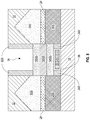
Referring now to FIG. 9, there is illustrated the exemplary semiconductor structure of FIG. 8 after forming a second functional gate structure (42, 44) of a second conductivity type that is opposite from the first conductivity type above the second silicon channel material nanosheet 18NS and in an area previously including the sacrificial gate structure 20 (i.e., the upper gate cavity portion 34). The second functional gate structure (42, 44) may include a second gate dielectric portion 42 and a second gate conductor portion 44.
The second gate dielectric portion 42 may include one of the gate dielectric materials mentioned above for the first gate dielectric portion 38. In one embodiment, the second gate dielectric portion 42 may include a same gate dielectric material as the first gate dielectric portion 38. In another embodiment, the second gate dielectric portion 42 may include a different gate dielectric material than the first gate dielectric portion 38. The second gate conductor portion 44 typically includes a different gate conductor material than the first gate conductor portion 40. The second functional gate structure (42, 44) can be formed by deposition of the gate dielectric material and the gate conductor material, and then planarizing the material stack of the deposited gate dielectric material and the gate conductor material such that a second functional gate structure (42, 44) has a topmost surface that is coplanar with a topmost surface of the topmost inner gate spacers 22S and the ILD material layer 32.
FIG. 9 illustrates a semiconductor structure of the present application and including a nanosheet stack comprising an epitaxial oxide nanosheet 16NS sandwiched between a first silicon channel material nanosheet 14NS and a second silicon channel material nanosheet 18NS, and suspended above a semiconductor substrate 10. A first field effect transistor (i.e., the first functional gate structure (38, 40)) of a first conductivity type is located beneath the first silicon channel material nanosheet 14NS, and a second field effect transistor (i.e., the second functional gate structure (42, 44)) of a second conductivity type, opposite the first conductivity type, is located above the second silicon channel material nanosheet 18NS. The exemplary structure of FIG. 9 takes up only one areal device. Thus, there is a density advantage with the exemplary semiconductor structure as compared to other structures in which the pFETs and nFETs are arranged side by side instead of vertically stacked as in the present application. Also, the epitaxial oxide nanosheet 16NS can serve as a charge storage element of the structure. Thus, the exemplary structure may be used as an EPROM device.
Referring now to FIG. 10, there is illustrated the exemplary semiconductor structure of FIG. 9 after forming contact structures (namely, first source/drain contact structure 46, second source/drain contact structure 48, and a ground contact structure 50). FIG. 10 also shows the presence of a dielectric isolation structure 11 that is formed on, or within, the semiconductor substrate 10. The dielectric isolation structure 11 may include a silicon dioxide layer that is formed after forming the nanosheet stacks 15 utilizing techniques well known to those skilled in the art.
The various contact structures (46, 48, 50) can be formed by first providing contact openings to expose a source/drain structure of the structure. The contact openings can be formed by lithography and etching. Each contact opening is the filled with a contact metal or metal alloy. Examples of contact metals include, but are not limited to, tungsten (W), aluminum (Al), copper (Cu), or cobalt (Co). An example of a contact metal alloy is Cu—Al alloy. A planarization process may follow the filling of each contact opening with the contact metal or metal alloy. The various contact structures (46, 48, 50) are embedded in the ILD material 32.
Referring now to FIG. 11, there is illustrated a basic circuit schematic of the exemplary structure of the present application. In the drawing, a charge storage region, i.e., the epitaxial oxide nanosheet 16NS, is sandwiched between a pFET (i.e., the second functional gate structure (42, 44)) and an nFET (i.e., the first functional gate structure (38, 40)). In this circuit, electrons in the charge storage region, i.e., the epitaxial oxide nanosheet 16NS, turn on the back channel of the pFET, making the pFET behave like a super-low-threshold voltage pFET, and turn off the nFET back channel, making the nFET behave like a super-high-threshold voltage nFET. Efficient hot electrons injection into the charge storage region is accomplished by avalanche hot electron injection using the pFET.
Referring now to FIG. 12, there is illustrated a circuit schematic when the exemplary structure of the present application operates as a CMOS inverter. In this instance, the exemplary structure operates as a CMOS EPROM. With no electrons in the charge storage region (i.e., the epitaxial oxide nanosheet 16) like a regular CMOS inverter: (i) Vout=Vss when Vgate=Vdd; and (ii) Vout=Vdd when Vgate=Vss.
With a sufficient number of electrons in the charge storage region, the pFET back channel is tuned on, while the nFET threshold voltage is increased. In this instance, (i) Vout approaches Vdd (>>Vdd/2) when Vgate=Vdd; and (ii) Vout=Vdd when Vgate=Vss. Thus, once programmed with hot electron injection, Vout is stuck near Vdd irrespective of Vgate.
Referring now to FIG. 13, there is illustrated a circuit schematic showing a 3×3 CMOS EPROM array including the exemplary structure of the present application. In array, the select line (SL) voltage is typically 0 (ground). To program a cell, wordline (WL0) is set a 3 V and the bitline L (BLL0) is set at 0 volts and the bitline R (BLR0) is set a 3V. The nFET is turned on, but there is no current flow in the nFET because BLL0 voltage is zero. The pFET is turned off, and avalanche hot electron injection occurs in the pFET. The larger the voltage of BLR0, the faster the hot electron injection rate. In programming, the non-selected cell has word line voltage of 0. Thus, the non-selected cell has its pFET turned on. Avalanche hot electron in a pFET is much less in a pFET that is on then in a pFET that is off. Hence, a non-selected cell would not be programmed unintentionally.
While the present application has been particularly shown and described with respect to preferred embodiments thereof, it will be understood by those skilled in the art that the foregoing and other changes in forms and details may be made without departing from the spirit and scope of the present application. It is therefore intended that the present application not be limited to the exact forms and details described and illustrated, but fall within the scope of the appended claims.

Claims (9)

What is claimed is:
1. A semiconductor structure comprising:
a nanosheet stack comprising an epitaxial oxide nanosheet sandwiched between a first silicon channel material nanosheet, wherein the nanosheet stack is suspended above a semiconductor substrate, and the epitaxial oxide nanosheet has a first surface that is in direct physical contact with an entirety of a surface of the first silicon channel material nanosheet, and a second surface, which is opposite the first surface, that is in direct physical contact with an entirety of a surface of the second silicon channel material nanosheet;
a first field effect transistor of a first conductivity type located beneath the first silicon channel material nanosheet;
a second field effect transistor of a second conductivity type, opposite the first conductivity type, located above the second silicon channel material nanosheet;
a first source/drain structure located on each side of the nanosheet stack and in direct physical contact with a sidewall of the first silicon channel material nanosheet and a lower portion of a sidewall of the epitaxial oxide nanosheet; and
a second source/drain structure located on each side of the nanosheet stack and in direct physical contact with a sidewall of the second silicon channel material nanosheet and an upper portion of the sidewall of the epitaxial oxide nanosheet.
2. The semiconductor structure of claim 1, wherein electrons are stored in the epitaxial oxide nanosheet.
3. The semiconductor structure of claim 1, wherein the epitaxial oxide nanosheet, the first silicon channel material nanosheet and the second silicon channel material nanosheet are lattice matched.
4. The semiconductor structure of claim 1, wherein the sidewalls of the epitaxial oxide nanosheet are vertically aligned to the sidewalls of both the first silicon channel material nanosheet and the second silicon channel material.
5. The semiconductor structure of claim 1, further comprising an inner spacer surrounding the first field effect transistor and another inner spacer surrounding the second field effect transistor.
6. The semiconductor structure of claim 1, further comprising a dielectric material layer separating the first and second source/drain structures, and directly contacting a middle portion of the sidewall of the epitaxial oxide nanosheet.
7. The semiconductor structure of claim 1, wherein the first conductivity type is n-type and the second conductivity type is p-type.
8. The semiconductor structure of claim 3, wherein the epitaxial oxide nanosheet is composed of lanthanum (II) oxide, gadolinium(III)-oxide, dysprosium(III)-oxide, holmium(III) oxide, erbium (III) oxide, thulium (III) oxide, lutetium(III) oxide, cerium (IV) oxide, lanthanum-yttrium oxide, gadolinium-erbium oxide, neodymium-erbium oxide, neodymium-gadolinium oxide, or lanthanum-erbium oxide.
9. The semiconductor structure of claim 1, further comprising a dielectric isolation structure located on the semiconductor substrate.
US16/050,810 2018-07-31 2018-07-31 Nanosheet-CMOS EPROM device with epitaxial oxide charge storage region Active US10916629B2 (en)

Priority Applications (1)

Application Number Priority Date Filing Date Title
US16/050,810 US10916629B2 (en) 2018-07-31 2018-07-31 Nanosheet-CMOS EPROM device with epitaxial oxide charge storage region

Applications Claiming Priority (1)

Application Number Priority Date Filing Date Title
US16/050,810 US10916629B2 (en) 2018-07-31 2018-07-31 Nanosheet-CMOS EPROM device with epitaxial oxide charge storage region

Publications (2)

Publication Number Publication Date
US20200044028A1 US20200044028A1 (en) 2020-02-06
US10916629B2 true US10916629B2 (en) 2021-02-09

Family

ID=69227854

Family Applications (1)

Application Number Title Priority Date Filing Date
US16/050,810 Active US10916629B2 (en) 2018-07-31 2018-07-31 Nanosheet-CMOS EPROM device with epitaxial oxide charge storage region

Country Status (1)

Country Link
US (1) US10916629B2 (en)

Families Citing this family (2)

* Cited by examiner, † Cited by third party
Publication number Priority date Publication date Assignee Title
US10832969B2 (en) * 2018-10-15 2020-11-10 International Business Machines Corporation Single-fin CMOS transistors with embedded and cladded source/drain structures
US11715777B2 (en) * 2020-05-29 2023-08-01 Taiwan Semiconductor Manufacturing Co., Ltd. Semiconductor device and method

Citations (16)

* Cited by examiner, † Cited by third party
Publication number Priority date Publication date Assignee Title
US6610548B1 (en) 1999-03-26 2003-08-26 Sony Corporation Crystal growth method of oxide, cerium oxide, promethium oxide, multi-layered structure of oxides, manufacturing method of field effect transistor, manufacturing method of ferroelectric non-volatile memory and ferroelectric non-volatile memory
US6630383B1 (en) 2002-09-23 2003-10-07 Advanced Micro Devices, Inc. Bi-layer floating gate for improved work function between floating gate and a high-K dielectric layer
US6852575B2 (en) 2001-07-05 2005-02-08 International Business Machines Corporation Method of forming lattice-matched structure on silicon and structure formed thereby
US7135699B1 (en) 2000-08-08 2006-11-14 Translucent Photonics, Inc. Method and apparatus for growth of single-crystal rare-earth oxides, nitrides, and phosphides
US7183606B2 (en) 2003-09-05 2007-02-27 Powerchip Semiconductor Corp. Flash memory cell and manufacturing method thereof
US7700993B2 (en) 2007-11-05 2010-04-20 International Business Machines Corporation CMOS EPROM and EEPROM devices and programmable CMOS inverters
US8705280B2 (en) 2010-05-25 2014-04-22 International Business Machines Corporation Electrically programmable floating common gate CMOS device and applications thereof
US9224811B2 (en) * 2014-03-17 2015-12-29 Globalfoundries Inc Stacked semiconductor device
US20160043074A1 (en) * 2013-04-05 2016-02-11 University College Cork - National University Of Ireland, Cork Junctionless nanowire transistors for 3d monolithic integration of cmos inverters
US20160204228A1 (en) * 2015-01-13 2016-07-14 Tokyo Electron Limited Method for forming a nanowire structure
US9472558B1 (en) * 2015-11-13 2016-10-18 Globalfoundries Inc. Semiconductor structures with stacked non-planar field effect transistors and methods of forming the structures
US20160322478A1 (en) 2008-05-28 2016-11-03 Micron Technology, Inc. Methods Of Forming Transistor Gates
US9659655B1 (en) 2016-09-08 2017-05-23 International Business Machines Corporation Memory arrays using common floating gate series devices
US20180019255A1 (en) 2016-07-12 2018-01-18 Micron Technology, Inc. Elevationally-Extending String Of Memory Cells Individually Comprising A Programmable Charge Storage Transistor And Method Of Forming An Elevationally-Extending String Of Memory Cells Individually Comprising A Programmable Charge Storage Transistor
US9881930B1 (en) 2016-10-21 2018-01-30 International Business Machines Corporation Simple integration of non-volatile memory and complementary metal oxide semiconductor
US20180374753A1 (en) * 2017-06-22 2018-12-27 Globalfoundries Inc. Stacked elongated nanoshapes of different semiconductor materials and structures that incorporate the nanoshapes

Patent Citations (16)

* Cited by examiner, † Cited by third party
Publication number Priority date Publication date Assignee Title
US6610548B1 (en) 1999-03-26 2003-08-26 Sony Corporation Crystal growth method of oxide, cerium oxide, promethium oxide, multi-layered structure of oxides, manufacturing method of field effect transistor, manufacturing method of ferroelectric non-volatile memory and ferroelectric non-volatile memory
US7135699B1 (en) 2000-08-08 2006-11-14 Translucent Photonics, Inc. Method and apparatus for growth of single-crystal rare-earth oxides, nitrides, and phosphides
US6852575B2 (en) 2001-07-05 2005-02-08 International Business Machines Corporation Method of forming lattice-matched structure on silicon and structure formed thereby
US6630383B1 (en) 2002-09-23 2003-10-07 Advanced Micro Devices, Inc. Bi-layer floating gate for improved work function between floating gate and a high-K dielectric layer
US7183606B2 (en) 2003-09-05 2007-02-27 Powerchip Semiconductor Corp. Flash memory cell and manufacturing method thereof
US7700993B2 (en) 2007-11-05 2010-04-20 International Business Machines Corporation CMOS EPROM and EEPROM devices and programmable CMOS inverters
US20160322478A1 (en) 2008-05-28 2016-11-03 Micron Technology, Inc. Methods Of Forming Transistor Gates
US8705280B2 (en) 2010-05-25 2014-04-22 International Business Machines Corporation Electrically programmable floating common gate CMOS device and applications thereof
US20160043074A1 (en) * 2013-04-05 2016-02-11 University College Cork - National University Of Ireland, Cork Junctionless nanowire transistors for 3d monolithic integration of cmos inverters
US9224811B2 (en) * 2014-03-17 2015-12-29 Globalfoundries Inc Stacked semiconductor device
US20160204228A1 (en) * 2015-01-13 2016-07-14 Tokyo Electron Limited Method for forming a nanowire structure
US9472558B1 (en) * 2015-11-13 2016-10-18 Globalfoundries Inc. Semiconductor structures with stacked non-planar field effect transistors and methods of forming the structures
US20180019255A1 (en) 2016-07-12 2018-01-18 Micron Technology, Inc. Elevationally-Extending String Of Memory Cells Individually Comprising A Programmable Charge Storage Transistor And Method Of Forming An Elevationally-Extending String Of Memory Cells Individually Comprising A Programmable Charge Storage Transistor
US9659655B1 (en) 2016-09-08 2017-05-23 International Business Machines Corporation Memory arrays using common floating gate series devices
US9881930B1 (en) 2016-10-21 2018-01-30 International Business Machines Corporation Simple integration of non-volatile memory and complementary metal oxide semiconductor
US20180374753A1 (en) * 2017-06-22 2018-12-27 Globalfoundries Inc. Stacked elongated nanoshapes of different semiconductor materials and structures that incorporate the nanoshapes

Non-Patent Citations (2)

* Cited by examiner, † Cited by third party
Title
Shi, R., et al, "Nb-Doped La2O3 as Charge-Trapping Layer for Nonvolatile Memory Applications", IEEE Transactions on Device and Materials Reliability, Mar. 2015, pp. 123-126, vol. 15, No. 1.
Tao, Q. B., "Mo-Doped La2O3 as Charge-Trapping Layer for Improved Low-Voltage Flash-Memory Performance", ECS Solid State Letters, Published Aug. 31, 2013, pp. Q87-Q89, 2 (11).

Also Published As

Publication number Publication date
US20200044028A1 (en) 2020-02-06

Similar Documents

Publication Publication Date Title
US10770461B2 (en) Enhanced field resistive RAM integrated with nanosheet technology
US10756216B2 (en) Nanosheet mosfet with isolated source/drain epitaxy and close junction proximity
US10886368B2 (en) I/O device scheme for gate-all-around transistors
US10243043B2 (en) Self-aligned air gap spacer for nanosheet CMOS devices
US10593673B2 (en) Nanosheet with single epitaxial stack forming off-set dual material channels for gate-all-around CMOS
US10468311B2 (en) Nanosheet substrate isolated source/drain epitaxy by nitrogen implantation
US10374039B1 (en) Enhanced field bipolar resistive RAM integrated with FDSOI technology
US10566349B2 (en) FinFET with stacked faceted S/D epitaxy for improved contact resistance
US9799777B1 (en) Floating gate memory in a channel last vertical FET flow
US11038103B2 (en) Tightly integrated 1T1R ReRAM for planar technology
US11302813B2 (en) Wrap around contact for nanosheet source drain epitaxy
US10559692B2 (en) Nanosheet substrate isolation scheme by lattice matched wide bandgap semiconductor
US9947675B1 (en) Mask-programmable ROM using a vertical FET integration process
US20190378842A1 (en) NANOSHEET eDRAM
US9614077B1 (en) Vertical finfet with strained channel
US11177369B2 (en) Stacked vertical field effect transistor with self-aligned junctions
US20220328633A1 (en) Ge based semiconductor device and a method for manufacturing the same
US10916629B2 (en) Nanosheet-CMOS EPROM device with epitaxial oxide charge storage region
US10903360B1 (en) Vertically integrated memory cells with complementary pass transistor selectors
US9831254B1 (en) Multiple breakdown point low resistance anti-fuse structure
US10304841B2 (en) Metal FinFET anti-fuse
US11075301B2 (en) Nanosheet with buried gate contact
US20230290821A1 (en) Self-aligned contact (sac) in nanosheet transistors
US20230178597A1 (en) Semiconductor structures with low top contact resistance

Legal Events

Date Code Title Description
AS Assignment

Owner name: INTERNATIONAL BUSINESS MACHINES CORPORATION, NEW YORK

Free format text: ASSIGNMENT OF ASSIGNORS INTEREST;ASSIGNORS:REZNICEK, ALEXANDER;YAU, JENG-BANG;NING, TAK H.;AND OTHERS;SIGNING DATES FROM 20180724 TO 20180730;REEL/FRAME:046515/0657

FEPP Fee payment procedure

Free format text: ENTITY STATUS SET TO UNDISCOUNTED (ORIGINAL EVENT CODE: BIG.); ENTITY STATUS OF PATENT OWNER: LARGE ENTITY

STPP Information on status: patent application and granting procedure in general

Free format text: NON FINAL ACTION MAILED

STPP Information on status: patent application and granting procedure in general

Free format text: RESPONSE AFTER FINAL ACTION FORWARDED TO EXAMINER

STPP Information on status: patent application and granting procedure in general

Free format text: NON FINAL ACTION MAILED

STCF Information on status: patent grant

Free format text: PATENTED CASE