US10914780B2 - Methods and apparatuses for threshold voltage measurement and related semiconductor devices and systems - Google Patents
Methods and apparatuses for threshold voltage measurement and related semiconductor devices and systems Download PDFInfo
- Publication number
- US10914780B2 US10914780B2 US16/227,348 US201816227348A US10914780B2 US 10914780 B2 US10914780 B2 US 10914780B2 US 201816227348 A US201816227348 A US 201816227348A US 10914780 B2 US10914780 B2 US 10914780B2
- Authority
- US
- United States
- Prior art keywords
- transistor
- circuit
- voltage
- operational amplifier
- coupled
- Prior art date
- Legal status (The legal status is an assumption and is not a legal conclusion. Google has not performed a legal analysis and makes no representation as to the accuracy of the status listed.)
- Active, expires
Links
Images


Classifications
-
- G—PHYSICS
- G05—CONTROLLING; REGULATING
- G05F—SYSTEMS FOR REGULATING ELECTRIC OR MAGNETIC VARIABLES
- G05F3/00—Non-retroactive systems for regulating electric variables by using an uncontrolled element, or an uncontrolled combination of elements, such element or such combination having self-regulating properties
- G05F3/02—Regulating voltage or current
- G05F3/08—Regulating voltage or current wherein the variable is DC
- G05F3/10—Regulating voltage or current wherein the variable is DC using uncontrolled devices with non-linear characteristics
- G05F3/16—Regulating voltage or current wherein the variable is DC using uncontrolled devices with non-linear characteristics being semiconductor devices
- G05F3/20—Regulating voltage or current wherein the variable is DC using uncontrolled devices with non-linear characteristics being semiconductor devices using diode- transistor combinations
- G05F3/26—Current mirrors
- G05F3/262—Current mirrors using field-effect transistors only
-
- G—PHYSICS
- G01—MEASURING; TESTING
- G01R—MEASURING ELECTRIC VARIABLES; MEASURING MAGNETIC VARIABLES
- G01R19/00—Arrangements for measuring currents or voltages or for indicating presence or sign thereof
- G01R19/165—Indicating that current or voltage is either above or below a predetermined value or within or outside a predetermined range of values
- G01R19/16528—Indicating that current or voltage is either above or below a predetermined value or within or outside a predetermined range of values using digital techniques or performing arithmetic operations
-
- G—PHYSICS
- G01—MEASURING; TESTING
- G01R—MEASURING ELECTRIC VARIABLES; MEASURING MAGNETIC VARIABLES
- G01R31/00—Arrangements for testing electric properties; Arrangements for locating electric faults; Arrangements for electrical testing characterised by what is being tested not provided for elsewhere
- G01R31/26—Testing of individual semiconductor devices
- G01R31/2607—Circuits therefor
- G01R31/2621—Circuits therefor for testing field effect transistors, i.e. FET's
-
- H—ELECTRICITY
- H03—ELECTRONIC CIRCUITRY
- H03F—AMPLIFIERS
- H03F3/00—Amplifiers with only discharge tubes or only semiconductor devices as amplifying elements
- H03F3/34—DC amplifiers in which all stages are DC-coupled
- H03F3/343—DC amplifiers in which all stages are DC-coupled with semiconductor devices only
- H03F3/347—DC amplifiers in which all stages are DC-coupled with semiconductor devices only in integrated circuits
-
- H—ELECTRICITY
- H03—ELECTRONIC CIRCUITRY
- H03F—AMPLIFIERS
- H03F3/00—Amplifiers with only discharge tubes or only semiconductor devices as amplifying elements
- H03F3/45—Differential amplifiers
- H03F3/45071—Differential amplifiers with semiconductor devices only
- H03F3/45076—Differential amplifiers with semiconductor devices only characterised by the way of implementation of the active amplifying circuit in the differential amplifier
- H03F3/45475—Differential amplifiers with semiconductor devices only characterised by the way of implementation of the active amplifying circuit in the differential amplifier using IC blocks as the active amplifying circuit
-
- H—ELECTRICITY
- H03—ELECTRONIC CIRCUITRY
- H03F—AMPLIFIERS
- H03F3/00—Amplifiers with only discharge tubes or only semiconductor devices as amplifying elements
- H03F3/50—Amplifiers in which input is applied to, or output is derived from, an impedance common to input and output circuits of the amplifying element, e.g. cathode follower
- H03F3/505—Amplifiers in which input is applied to, or output is derived from, an impedance common to input and output circuits of the amplifying element, e.g. cathode follower with field-effect devices
-
- H—ELECTRICITY
- H03—ELECTRONIC CIRCUITRY
- H03F—AMPLIFIERS
- H03F2200/00—Indexing scheme relating to amplifiers
- H03F2200/261—Amplifier which being suitable for instrumentation applications
-
- H—ELECTRICITY
- H03—ELECTRONIC CIRCUITRY
- H03F—AMPLIFIERS
- H03F2203/00—Indexing scheme relating to amplifiers with only discharge tubes or only semiconductor devices as amplifying elements covered by H03F3/00
- H03F2203/45—Indexing scheme relating to differential amplifiers
- H03F2203/45138—Two or more differential amplifiers in IC-block form are combined, e.g. measuring amplifiers
-
- H—ELECTRICITY
- H03—ELECTRONIC CIRCUITRY
- H03K—PULSE TECHNIQUE
- H03K19/00—Logic circuits, i.e. having at least two inputs acting on one output; Inverting circuits
- H03K19/02—Logic circuits, i.e. having at least two inputs acting on one output; Inverting circuits using specified components
- H03K19/08—Logic circuits, i.e. having at least two inputs acting on one output; Inverting circuits using specified components using semiconductor devices
- H03K19/094—Logic circuits, i.e. having at least two inputs acting on one output; Inverting circuits using specified components using semiconductor devices using field-effect transistors
- H03K19/0944—Logic circuits, i.e. having at least two inputs acting on one output; Inverting circuits using specified components using semiconductor devices using field-effect transistors using MOSFET or insulated gate field-effect transistors, i.e. IGFET
- H03K19/0948—Logic circuits, i.e. having at least two inputs acting on one output; Inverting circuits using specified components using semiconductor devices using field-effect transistors using MOSFET or insulated gate field-effect transistors, i.e. IGFET using CMOS or complementary insulated gate field-effect transistors
Definitions
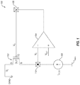
- FIG. 1 depicts a measurement circuit 100 including a transistor 102 , an operational amplifier 104 , and a current source 106 .
- Transistor 102 which may also be referred to as a device under test (DUT), includes a source S, a drain D, and a gate G.
- Circuit 100 which may include an integrated circuit, further includes pads 108 and 110 .
- Pad 108 is positioned and configured to measure a voltage V G at gate G of transistor 102
- pad 110 is positioned and configured to measure a voltage V S at source S of transistor 102 . More specifically, pad 108 may enable voltage V G to be measured (“probed”) via an external instrument. Further, pad 110 may enable voltage V S to be measured (“probed”) via an external instrument.
- Pads 108 and 110 , and associated measurement cables (not shown in FIG. 1 ), have relatively large parasitic capacitances (e.g., 200-400 picofarads (pF)).
- a number of amplifying stages in a feedback path of circuit 200 may be eight (i.e., assuming operational amplifiers 206 , 208 , and 210 are 2-stage operational amplifiers).
- the number of amplifying stages may result in additional capacitive nodes in the feedback path and stringent circuit design constraints on operational amplifiers 206 , 208 , and 210 (i.e., to achieve the required phase margin across PVT variations). Further, large compensating capacitors may be required to achieve stability, thus requiring a larger area.
- a number of amplifying stages in a feedback path (i.e., including operational amplifier 302 ) of measurement circuit 300 may be reduced (e.g., to three).
- an area of circuit 300 may be reduced compared to conventional circuits.
- circuit 400 to initiate a measurement mode, current I, which may be generated via current source 304 , may be supplied to transistor 308 via current mirror 306 .
- a constant current e.g., current I
- a drain of transistor 308 may be at, for example, zero volts and reference voltage V REF may be supplied to an input (e.g., non-inverting input) of operational amplifier 302 .
- circuit 400 may be reduced (e.g., to three).
- a number of amplifying stages in a feedback path i.e., including operational amplifier 302
- circuit 400 may be easier to stabilize circuit 400 (e.g., across PVT variations), and design constraints for maintaining stability across PVT variations may be relaxed.
- an area of circuit 400 may be reduced compared to conventional circuits.
- a voltage indicated by signal 502 at time T 0 may represent the voltage applied to a gate of the transistor (e.g., gate G of transistor 308 ; see FIG. 3 and/or FIG. 4 ) of the measurement circuit during an operational mode. Further, at time T 0 , the measurement circuit (e.g., circuit 300 of FIG. 3 or circuit 400 of FIG. 4 ) switches from the operational mode to a measurement mode. Moreover, the voltage indicated by signal 502 at time T 1 may represent the threshold voltage of the transistor (e.g., the threshold voltage of transistor 308 ; see FIG. 3 and/or FIG. 4 ).
- Plot 600 further depicts a control signal (indicate by signal 604 ), which is conveyed to the measurement circuit (i.e., including the transistor), for switching the measurement circuit from the operational mode to the measurement mode.
- a spike 603 in signal 602 may be due to switching from the operational mode to the measurement mode.
- Plot 600 further depicts a voltage (indicated by signal 606 ) at a current source (e.g., current source 304 of FIG. 3 or FIG. 4 ) of the measurement circuit.
- Plot 600 also depicts a current (indicated by signal 608 ) through a device under test (e.g., transistor 308 of FIG. 3 ) of the measurement circuit.
- the measurement circuit may include a dedicated ground, a dedicated supply line and/or a dedicated power line (e.g., the one or more sources are not shared with other circuitry, such as operational or switching circuitry), resulting in improved performance of the measurement circuitry.
- FIG. 8 is a flowchart of an example method 800 for measuring a threshold voltage of a transistor.
- Method 800 may be arranged in accordance with at least one embodiment described in the present disclosure.
- Method 800 may be performed, in some embodiments, by a device or system, such as circuit 300 of FIG. 3 , circuit 400 of FIG. 4 , device 850 of FIG. 9 , semiconductor device 900 of FIG. 10 , and/or system 1000 of FIG. 11 , or another device or system.
- a device or system such as circuit 300 of FIG. 3 , circuit 400 of FIG. 4 , device 850 of FIG. 9 , semiconductor device 900 of FIG. 10 , and/or system 1000 of FIG. 11 , or another device or system.
- a device or system such as circuit 300 of FIG. 3 , circuit 400 of FIG. 4 , device 850 of FIG. 9 , semiconductor device 900 of FIG. 10 , and/or system 1000 of FIG. 11 , or another device or system.
- FIG. 8 is a flowchart
- Method 800 may begin at block 802 , wherein a measurement mode for a circuit may be initiated, and method 800 may proceed to block 804 .
- Initiating the measurement mode may include, for example, switching the circuit from an operational (stress) mode to the measurement mode. Further, initiating the measurement mode may include, for example, conveying a current and/or a voltage to the circuit. More specifically, for example, with reference to FIGS. 3 and 4 , a current I, which may be generated via a current source (e.g., current source 304 ) and a current mirror (e.g., current mirror 306 ), may be supplied to transistor 308 of either circuit 300 or circuit 400 . Further, a reference voltage may be supplied to the circuit. More specifically, for example, with continued reference to FIGS. 3 and/or 4 , reference voltage V REF may be supplied to an input of operational amplifier 312 .
- method 800 may be implemented in differing order.
- the outlined operations and actions are only provided as examples, and some of the operations and actions may be optional, combined into fewer operations and actions, or expanded into additional operations and actions without detracting from the essence of the disclosed embodiment.
- a voltage at source of the transistor may be measured. More specifically, according to some embodiments, a voltage at an output of a unity-gain voltage follower, which is coupled to the source of the transistor, may be measured to determine a source voltage of the transistor. For example, with reference to FIG. 3 and/or FIG. 4 , a voltage at an output of operational amplifier 312 may be measured to determine voltage V S at source S of transistor 308 . For example, the voltage at the output of operational amplifier 312 may be measured via pad 316 . As another example, a current through the transistor (e.g., transistor 308 ) may be measured and/or a voltage at a current source (e.g., current source 304 ; see FIG. 3 and/or FIG. 4 ) may be measured.
- a current through the transistor e.g., transistor 308
- a voltage at a current source e.g., current source 304 ; see FIG. 3 and/or FIG. 4
- FIG. 9 depicts a device 850 including a measurement device 852 and an array 854 , according to various embodiments of the present disclosure.
- array 854 may include an array of transistors, and measurement device 852 may include circuitry for measuring a threshold voltage of one or more transistors of array 854 .
- measurement device 852 may include one or more of circuit 300 (see FIG. 3 ), one or more of circuit 400 (see FIG. 4 ), or any combination thereof.
- array 854 may include a memory array (e.g., a CMOS DRAM array) including a number of memory cells, wherein each cell may include at least one transistor.
- Memory device 1010 includes at least one memory cell (e.g., an array of memory cells), wherein one or more memory cells of memory device 1010 may include a transistor. Further, in some embodiments, one or more memory cells may include and/or may be associated with (e.g., coupled to) one or more measurement circuits according to one or more embodiments described herein.
- Electronic system 1000 may include a computing, processing, industrial, or consumer product. For example, without limitation, electronic system 1000 may include a personal computer or computer hardware component, a server or other networking hardware component, a handheld device, a tablet computer, an electronic notebook, a camera, a phone, a music player, a wireless device, a display, a chip set, a game, a vehicle, or other known systems.
- NBTI Negative Bias Temperature Instability
- Validation of NBTI models, wherein measurement delay may be critical may be carried out via one or more embodiments disclosed herein (e.g., circuit 300 of FIG. 3 and/or circuit 400 of FIG. 4 ). More specifically, various embodiments may allow for single point extraction of a transistor threshold voltage, with negligible NBTI recovery, in contrast to conventional devices that extract a threshold voltage from an “on” current and a subthreshold slope.
- the semiconductor device may include a memory array including at least one measurement circuit.
- the at least one measurement circuit may include a transistor and a first operational amplifier.
- the first operational amplifier may include a first input coupled to one of a source and a drain of the transistor and a second input configured to receive a reference voltage.
- the first operational amplifier may also include an output coupled to a gate of the transistor.
- the at least one measurement circuit may include a second operational amplifier.
- the second operational amplifier may include a first input coupled to the first input of the first operational amplifier.
- the second operational amplifier may include a second input coupled to an output of the second operational amplifier.
- Other embodiments of the present disclosure may include a method of measuring a threshold voltage of a transistor. Such a method may include initiating a measurement mode of a circuit including a transistor. The method may also include generating an output from a unity-gain voltage follower having an input coupled to the transistor. The method may further include measuring a threshold voltage of the transistor via an interface coupled to an output of the unity-gain voltage follower.
- any disjunctive word or phrase presenting two or more alternative terms, whether in the description, claims, or drawings, should be understood to contemplate the possibilities of including one of the terms, either of the terms, or both terms.
- the phrase “A or B” should be understood to include the possibilities of “A” or “B” or “A and B.”
Landscapes
- Engineering & Computer Science (AREA)
- Physics & Mathematics (AREA)
- Microelectronics & Electronic Packaging (AREA)
- General Physics & Mathematics (AREA)
- Power Engineering (AREA)
- Nonlinear Science (AREA)
- Electromagnetism (AREA)
- Radar, Positioning & Navigation (AREA)
- Automation & Control Theory (AREA)
- Semiconductor Integrated Circuits (AREA)
- Testing Of Individual Semiconductor Devices (AREA)
- Tests Of Electronic Circuits (AREA)
Abstract
Description
Claims (23)
Priority Applications (1)
| Application Number | Priority Date | Filing Date | Title |
|---|---|---|---|
| US16/227,348 US10914780B2 (en) | 2018-12-20 | 2018-12-20 | Methods and apparatuses for threshold voltage measurement and related semiconductor devices and systems |
Applications Claiming Priority (1)
| Application Number | Priority Date | Filing Date | Title |
|---|---|---|---|
| US16/227,348 US10914780B2 (en) | 2018-12-20 | 2018-12-20 | Methods and apparatuses for threshold voltage measurement and related semiconductor devices and systems |
Publications (2)
| Publication Number | Publication Date |
|---|---|
| US20200200816A1 US20200200816A1 (en) | 2020-06-25 |
| US10914780B2 true US10914780B2 (en) | 2021-02-09 |
Family
ID=71097528
Family Applications (1)
| Application Number | Title | Priority Date | Filing Date |
|---|---|---|---|
| US16/227,348 Active 2039-04-02 US10914780B2 (en) | 2018-12-20 | 2018-12-20 | Methods and apparatuses for threshold voltage measurement and related semiconductor devices and systems |
Country Status (1)
| Country | Link |
|---|---|
| US (1) | US10914780B2 (en) |
Families Citing this family (4)
| Publication number | Priority date | Publication date | Assignee | Title |
|---|---|---|---|---|
| US11217684B2 (en) * | 2019-05-19 | 2022-01-04 | Mikro Mesa Technology Co., Ltd. | Method for rapidly gathering sub-threshold swing from thin film transistor |
| CN115993514A (en) * | 2022-11-25 | 2023-04-21 | 广电计量检测集团股份有限公司 | A SiC Mosfet threshold voltage monitoring system and method |
| IT202300013689A1 (en) * | 2023-06-30 | 2024-12-30 | St Microelectronics Int Nv | MONITORING CIRCUIT AND CORRESPONDING PROCEDURE |
| US20260043841A1 (en) * | 2024-08-07 | 2026-02-12 | Semiconductor Components Industries, Llc | System and method for gate threshold voltage measurement |
Citations (12)
| Publication number | Priority date | Publication date | Assignee | Title |
|---|---|---|---|---|
| US4124475A (en) * | 1977-08-30 | 1978-11-07 | Delphian Corporation | Hydrogen sulfide monitoring system |
| US5039941A (en) | 1990-07-27 | 1991-08-13 | Intel Corporation | Voltage threshold measuring circuit |
| US5600594A (en) * | 1994-03-31 | 1997-02-04 | Sgs-Thomson Microelectronics S.R.L. | Threshold voltage measuring device for memory cells |
| US5792944A (en) * | 1993-08-31 | 1998-08-11 | Boehringer Mannheim Corporation | Power supply monitor and control for medical instrument |
| US20090066301A1 (en) * | 2007-09-07 | 2009-03-12 | Matsushita Electric Industrial Co., Ltd. | Buck-boost switching regulator |
| US20090302812A1 (en) * | 2008-06-05 | 2009-12-10 | Joseph Shor | Low noise voltage regulator |
| US20140111280A1 (en) * | 2012-10-19 | 2014-04-24 | Texas Instruments Deutschland Gmbh | Electronic device, fiber-optic communication system comprising the electronic device and method of operating the electronic device |
| US20140268909A1 (en) * | 2013-03-15 | 2014-09-18 | Linear Technology Corporation | Methods and systems for control of dc-dc converters |
| US20160005828A1 (en) * | 2014-07-01 | 2016-01-07 | Globalfoundries Inc. | Gate dielectric protection for transistors |
| US20170142798A1 (en) * | 2015-11-12 | 2017-05-18 | Fairchild (Taiwan) Corporation | Led driver |
| US20180080960A1 (en) * | 2016-09-16 | 2018-03-22 | STMicroelectronics (Alps) SAS | Method for determining the current consumption of an active load, for example a processing unit, and associated electronic device |
| US9989582B2 (en) * | 2015-07-02 | 2018-06-05 | SK Hynix Inc. | Device for measuring threshold voltage of a transistor based on constant drain voltage and constant drain source current |
-
2018
- 2018-12-20 US US16/227,348 patent/US10914780B2/en active Active
Patent Citations (12)
| Publication number | Priority date | Publication date | Assignee | Title |
|---|---|---|---|---|
| US4124475A (en) * | 1977-08-30 | 1978-11-07 | Delphian Corporation | Hydrogen sulfide monitoring system |
| US5039941A (en) | 1990-07-27 | 1991-08-13 | Intel Corporation | Voltage threshold measuring circuit |
| US5792944A (en) * | 1993-08-31 | 1998-08-11 | Boehringer Mannheim Corporation | Power supply monitor and control for medical instrument |
| US5600594A (en) * | 1994-03-31 | 1997-02-04 | Sgs-Thomson Microelectronics S.R.L. | Threshold voltage measuring device for memory cells |
| US20090066301A1 (en) * | 2007-09-07 | 2009-03-12 | Matsushita Electric Industrial Co., Ltd. | Buck-boost switching regulator |
| US20090302812A1 (en) * | 2008-06-05 | 2009-12-10 | Joseph Shor | Low noise voltage regulator |
| US20140111280A1 (en) * | 2012-10-19 | 2014-04-24 | Texas Instruments Deutschland Gmbh | Electronic device, fiber-optic communication system comprising the electronic device and method of operating the electronic device |
| US20140268909A1 (en) * | 2013-03-15 | 2014-09-18 | Linear Technology Corporation | Methods and systems for control of dc-dc converters |
| US20160005828A1 (en) * | 2014-07-01 | 2016-01-07 | Globalfoundries Inc. | Gate dielectric protection for transistors |
| US9989582B2 (en) * | 2015-07-02 | 2018-06-05 | SK Hynix Inc. | Device for measuring threshold voltage of a transistor based on constant drain voltage and constant drain source current |
| US20170142798A1 (en) * | 2015-11-12 | 2017-05-18 | Fairchild (Taiwan) Corporation | Led driver |
| US20180080960A1 (en) * | 2016-09-16 | 2018-03-22 | STMicroelectronics (Alps) SAS | Method for determining the current consumption of an active load, for example a processing unit, and associated electronic device |
Also Published As
| Publication number | Publication date |
|---|---|
| US20200200816A1 (en) | 2020-06-25 |
Similar Documents
| Publication | Publication Date | Title |
|---|---|---|
| US10914780B2 (en) | Methods and apparatuses for threshold voltage measurement and related semiconductor devices and systems | |
| KR930008661B1 (en) | Data input buffer of semiconductor memory apparatus | |
| US7868640B2 (en) | Array-based early threshold voltage recovery characterization measurement | |
| CN106656132B (en) | Extremely low electric leakage analog switch, chip and communication terminal | |
| US10837993B2 (en) | Circuit and method for bandwidth measurement | |
| US8779796B2 (en) | Method and apparatus for device parameter measurement | |
| US20130099825A1 (en) | Voltage comparator | |
| CN106990367B (en) | SoC on-chip power supply noise monitoring system | |
| US8582378B1 (en) | Threshold voltage measurement device | |
| US7692955B2 (en) | Semiconductor integrated circuit | |
| US20140266290A1 (en) | Process detection circuit | |
| US11289151B2 (en) | Cross-coupled transistor threshold voltage mismatch compensation and related devices, systems, and methods | |
| US11367476B2 (en) | Bit line equalization driver circuits and related apparatuses, methods, and computing systems to avoid degradation of pull-down transistors | |
| JP4151572B2 (en) | Transistor pair characteristic difference measuring device and characteristic difference measuring method | |
| US9762215B1 (en) | Apparatuses and methods for voltage buffering | |
| US8222952B2 (en) | Semiconductor device having a complementary field effect transistor | |
| Ji et al. | Operational amplifier based test structure for transistor threshold voltage variation | |
| TWI509267B (en) | Electric parameter test device that tests the electric parameters of a very-large-scale transistor array | |
| US11327112B2 (en) | Semiconductor device for detecting characteristics of semiconductor element and operating method thereof | |
| US7279922B1 (en) | Sub-sampling of weakly-driven nodes | |
| JP2771880B2 (en) | Semiconductor device | |
| US8594958B2 (en) | Method and apparatus of electrical device characterization | |
| US9673805B2 (en) | Leakage current reduction in stacked field-effect transistors | |
| JPH11330358A (en) | Substrate noise detection amplifier circuit | |
| Lynch et al. | A low power logic-compatible multi-bit memory bit cell architecture with differential pair and current stop constructs |
Legal Events
| Date | Code | Title | Description |
|---|---|---|---|
| AS | Assignment |
Owner name: MICRON TECHNOLOGY, INC., IDAHO Free format text: ASSIGNMENT OF ASSIGNORS INTEREST;ASSIGNORS:PANAKKAL, BINOY JOSE;GUPTA, RAJESH N.;SIGNING DATES FROM 20181115 TO 20181123;REEL/FRAME:047832/0397 |
|
| FEPP | Fee payment procedure |
Free format text: ENTITY STATUS SET TO UNDISCOUNTED (ORIGINAL EVENT CODE: BIG.); ENTITY STATUS OF PATENT OWNER: LARGE ENTITY |
|
| AS | Assignment |
Owner name: JPMORGAN CHASE BANK, N.A., AS COLLATERAL AGENT, ILLINOIS Free format text: SUPPLEMENT NO. 3 TO PATENT SECURITY AGREEMENT;ASSIGNOR:MICRON TECHNOLOGY, INC.;REEL/FRAME:048951/0902 Effective date: 20190416 Owner name: MORGAN STANLEY SENIOR FUNDING, INC., AS COLLATERAL AGENT, MARYLAND Free format text: SUPPLEMENT NO. 12 TO PATENT SECURITY AGREEMENT;ASSIGNOR:MICRON TECHNOLOGY, INC.;REEL/FRAME:048948/0677 Effective date: 20190416 |
|
| AS | Assignment |
Owner name: MICRON TECHNOLOGY, INC., IDAHO Free format text: RELEASE BY SECURED PARTY;ASSIGNOR:MORGAN STANLEY SENIOR FUNDING, INC., AS COLLATERAL AGENT;REEL/FRAME:050724/0392 Effective date: 20190731 |
|
| AS | Assignment |
Owner name: MICRON TECHNOLOGY, INC., IDAHO Free format text: RELEASE BY SECURED PARTY;ASSIGNOR:JPMORGAN CHASE BANK, N.A., AS COLLATERAL AGENT;REEL/FRAME:051041/0317 Effective date: 20190731 |
|
| STPP | Information on status: patent application and granting procedure in general |
Free format text: NON FINAL ACTION MAILED |
|
| STPP | Information on status: patent application and granting procedure in general |
Free format text: PUBLICATIONS -- ISSUE FEE PAYMENT RECEIVED |
|
| STPP | Information on status: patent application and granting procedure in general |
Free format text: PUBLICATIONS -- ISSUE FEE PAYMENT VERIFIED |
|
| STCF | Information on status: patent grant |
Free format text: PATENTED CASE |
|
| MAFP | Maintenance fee payment |
Free format text: PAYMENT OF MAINTENANCE FEE, 4TH YEAR, LARGE ENTITY (ORIGINAL EVENT CODE: M1551); ENTITY STATUS OF PATENT OWNER: LARGE ENTITY Year of fee payment: 4 |