US10910357B2 - Semiconductor package including hybrid bonding structure and method for preparing the same - Google Patents
Semiconductor package including hybrid bonding structure and method for preparing the same Download PDFInfo
- Publication number
- US10910357B2 US10910357B2 US16/360,619 US201916360619A US10910357B2 US 10910357 B2 US10910357 B2 US 10910357B2 US 201916360619 A US201916360619 A US 201916360619A US 10910357 B2 US10910357 B2 US 10910357B2
- Authority
- US
- United States
- Prior art keywords
- die
- barrier layer
- front side
- back side
- tsv
- Prior art date
- Legal status (The legal status is an assumption and is not a legal conclusion. Google has not performed a legal analysis and makes no representation as to the accuracy of the status listed.)
- Active
Links
Images


Classifications
-
- H—ELECTRICITY
- H01—ELECTRIC ELEMENTS
- H01L—SEMICONDUCTOR DEVICES NOT COVERED BY CLASS H10
- H01L25/00—Assemblies consisting of a plurality of individual semiconductor or other solid state devices ; Multistep manufacturing processes thereof
- H01L25/18—Assemblies consisting of a plurality of individual semiconductor or other solid state devices ; Multistep manufacturing processes thereof the devices being of types provided for in two or more different subgroups of the same main group of groups H01L27/00 - H01L33/00, or in a single subclass of H10K, H10N
-
- H—ELECTRICITY
- H01—ELECTRIC ELEMENTS
- H01L—SEMICONDUCTOR DEVICES NOT COVERED BY CLASS H10
- H01L23/00—Details of semiconductor or other solid state devices
- H01L23/28—Encapsulations, e.g. encapsulating layers, coatings, e.g. for protection
- H01L23/31—Encapsulations, e.g. encapsulating layers, coatings, e.g. for protection characterised by the arrangement or shape
- H01L23/3107—Encapsulations, e.g. encapsulating layers, coatings, e.g. for protection characterised by the arrangement or shape the device being completely enclosed
- H01L23/3121—Encapsulations, e.g. encapsulating layers, coatings, e.g. for protection characterised by the arrangement or shape the device being completely enclosed a substrate forming part of the encapsulation
- H01L23/3128—Encapsulations, e.g. encapsulating layers, coatings, e.g. for protection characterised by the arrangement or shape the device being completely enclosed a substrate forming part of the encapsulation the substrate having spherical bumps for external connection
-
- H—ELECTRICITY
- H01—ELECTRIC ELEMENTS
- H01L—SEMICONDUCTOR DEVICES NOT COVERED BY CLASS H10
- H01L21/00—Processes or apparatus adapted for the manufacture or treatment of semiconductor or solid state devices or of parts thereof
- H01L21/70—Manufacture or treatment of devices consisting of a plurality of solid state components formed in or on a common substrate or of parts thereof; Manufacture of integrated circuit devices or of parts thereof
- H01L21/71—Manufacture of specific parts of devices defined in group H01L21/70
- H01L21/768—Applying interconnections to be used for carrying current between separate components within a device comprising conductors and dielectrics
- H01L21/76898—Applying interconnections to be used for carrying current between separate components within a device comprising conductors and dielectrics formed through a semiconductor substrate
-
- H—ELECTRICITY
- H01—ELECTRIC ELEMENTS
- H01L—SEMICONDUCTOR DEVICES NOT COVERED BY CLASS H10
- H01L21/00—Processes or apparatus adapted for the manufacture or treatment of semiconductor or solid state devices or of parts thereof
- H01L21/70—Manufacture or treatment of devices consisting of a plurality of solid state components formed in or on a common substrate or of parts thereof; Manufacture of integrated circuit devices or of parts thereof
- H01L21/77—Manufacture or treatment of devices consisting of a plurality of solid state components or integrated circuits formed in, or on, a common substrate
- H01L21/78—Manufacture or treatment of devices consisting of a plurality of solid state components or integrated circuits formed in, or on, a common substrate with subsequent division of the substrate into plural individual devices
- H01L21/82—Manufacture or treatment of devices consisting of a plurality of solid state components or integrated circuits formed in, or on, a common substrate with subsequent division of the substrate into plural individual devices to produce devices, e.g. integrated circuits, each consisting of a plurality of components
- H01L21/822—Manufacture or treatment of devices consisting of a plurality of solid state components or integrated circuits formed in, or on, a common substrate with subsequent division of the substrate into plural individual devices to produce devices, e.g. integrated circuits, each consisting of a plurality of components the substrate being a semiconductor, using silicon technology
- H01L21/8221—Three dimensional integrated circuits stacked in different levels
-
- H—ELECTRICITY
- H01—ELECTRIC ELEMENTS
- H01L—SEMICONDUCTOR DEVICES NOT COVERED BY CLASS H10
- H01L23/00—Details of semiconductor or other solid state devices
- H01L23/48—Arrangements for conducting electric current to or from the solid state body in operation, e.g. leads, terminal arrangements ; Selection of materials therefor
- H01L23/481—Internal lead connections, e.g. via connections, feedthrough structures
-
- H—ELECTRICITY
- H01—ELECTRIC ELEMENTS
- H01L—SEMICONDUCTOR DEVICES NOT COVERED BY CLASS H10
- H01L23/00—Details of semiconductor or other solid state devices
- H01L23/48—Arrangements for conducting electric current to or from the solid state body in operation, e.g. leads, terminal arrangements ; Selection of materials therefor
- H01L23/488—Arrangements for conducting electric current to or from the solid state body in operation, e.g. leads, terminal arrangements ; Selection of materials therefor consisting of soldered or bonded constructions
- H01L23/498—Leads, i.e. metallisations or lead-frames on insulating substrates, e.g. chip carriers
- H01L23/49811—Additional leads joined to the metallisation on the insulating substrate, e.g. pins, bumps, wires, flat leads
- H01L23/49816—Spherical bumps on the substrate for external connection, e.g. ball grid arrays [BGA]
-
- H—ELECTRICITY
- H01—ELECTRIC ELEMENTS
- H01L—SEMICONDUCTOR DEVICES NOT COVERED BY CLASS H10
- H01L23/00—Details of semiconductor or other solid state devices
- H01L23/48—Arrangements for conducting electric current to or from the solid state body in operation, e.g. leads, terminal arrangements ; Selection of materials therefor
- H01L23/488—Arrangements for conducting electric current to or from the solid state body in operation, e.g. leads, terminal arrangements ; Selection of materials therefor consisting of soldered or bonded constructions
- H01L23/498—Leads, i.e. metallisations or lead-frames on insulating substrates, e.g. chip carriers
- H01L23/49827—Via connections through the substrates, e.g. pins going through the substrate, coaxial cables
-
- H—ELECTRICITY
- H01—ELECTRIC ELEMENTS
- H01L—SEMICONDUCTOR DEVICES NOT COVERED BY CLASS H10
- H01L23/00—Details of semiconductor or other solid state devices
- H01L23/48—Arrangements for conducting electric current to or from the solid state body in operation, e.g. leads, terminal arrangements ; Selection of materials therefor
- H01L23/488—Arrangements for conducting electric current to or from the solid state body in operation, e.g. leads, terminal arrangements ; Selection of materials therefor consisting of soldered or bonded constructions
- H01L23/498—Leads, i.e. metallisations or lead-frames on insulating substrates, e.g. chip carriers
- H01L23/49838—Geometry or layout
-
- H—ELECTRICITY
- H01—ELECTRIC ELEMENTS
- H01L—SEMICONDUCTOR DEVICES NOT COVERED BY CLASS H10
- H01L23/00—Details of semiconductor or other solid state devices
- H01L23/52—Arrangements for conducting electric current within the device in operation from one component to another, i.e. interconnections, e.g. wires, lead frames
- H01L23/522—Arrangements for conducting electric current within the device in operation from one component to another, i.e. interconnections, e.g. wires, lead frames including external interconnections consisting of a multilayer structure of conductive and insulating layers inseparably formed on the semiconductor body
- H01L23/5226—Via connections in a multilevel interconnection structure
-
- H—ELECTRICITY
- H01—ELECTRIC ELEMENTS
- H01L—SEMICONDUCTOR DEVICES NOT COVERED BY CLASS H10
- H01L23/00—Details of semiconductor or other solid state devices
- H01L23/52—Arrangements for conducting electric current within the device in operation from one component to another, i.e. interconnections, e.g. wires, lead frames
- H01L23/522—Arrangements for conducting electric current within the device in operation from one component to another, i.e. interconnections, e.g. wires, lead frames including external interconnections consisting of a multilayer structure of conductive and insulating layers inseparably formed on the semiconductor body
- H01L23/528—Geometry or layout of the interconnection structure
- H01L23/5283—Cross-sectional geometry
-
- H—ELECTRICITY
- H01—ELECTRIC ELEMENTS
- H01L—SEMICONDUCTOR DEVICES NOT COVERED BY CLASS H10
- H01L24/00—Arrangements for connecting or disconnecting semiconductor or solid-state bodies; Methods or apparatus related thereto
- H01L24/01—Means for bonding being attached to, or being formed on, the surface to be connected, e.g. chip-to-package, die-attach, "first-level" interconnects; Manufacturing methods related thereto
- H01L24/02—Bonding areas ; Manufacturing methods related thereto
- H01L24/07—Structure, shape, material or disposition of the bonding areas after the connecting process
- H01L24/08—Structure, shape, material or disposition of the bonding areas after the connecting process of an individual bonding area
-
- H—ELECTRICITY
- H01—ELECTRIC ELEMENTS
- H01L—SEMICONDUCTOR DEVICES NOT COVERED BY CLASS H10
- H01L24/00—Arrangements for connecting or disconnecting semiconductor or solid-state bodies; Methods or apparatus related thereto
- H01L24/01—Means for bonding being attached to, or being formed on, the surface to be connected, e.g. chip-to-package, die-attach, "first-level" interconnects; Manufacturing methods related thereto
- H01L24/02—Bonding areas ; Manufacturing methods related thereto
- H01L24/07—Structure, shape, material or disposition of the bonding areas after the connecting process
- H01L24/09—Structure, shape, material or disposition of the bonding areas after the connecting process of a plurality of bonding areas
-
- H—ELECTRICITY
- H01—ELECTRIC ELEMENTS
- H01L—SEMICONDUCTOR DEVICES NOT COVERED BY CLASS H10
- H01L24/00—Arrangements for connecting or disconnecting semiconductor or solid-state bodies; Methods or apparatus related thereto
- H01L24/01—Means for bonding being attached to, or being formed on, the surface to be connected, e.g. chip-to-package, die-attach, "first-level" interconnects; Manufacturing methods related thereto
- H01L24/10—Bump connectors ; Manufacturing methods related thereto
- H01L24/15—Structure, shape, material or disposition of the bump connectors after the connecting process
- H01L24/17—Structure, shape, material or disposition of the bump connectors after the connecting process of a plurality of bump connectors
-
- H—ELECTRICITY
- H01—ELECTRIC ELEMENTS
- H01L—SEMICONDUCTOR DEVICES NOT COVERED BY CLASS H10
- H01L24/00—Arrangements for connecting or disconnecting semiconductor or solid-state bodies; Methods or apparatus related thereto
- H01L24/01—Means for bonding being attached to, or being formed on, the surface to be connected, e.g. chip-to-package, die-attach, "first-level" interconnects; Manufacturing methods related thereto
- H01L24/26—Layer connectors, e.g. plate connectors, solder or adhesive layers; Manufacturing methods related thereto
- H01L24/31—Structure, shape, material or disposition of the layer connectors after the connecting process
- H01L24/33—Structure, shape, material or disposition of the layer connectors after the connecting process of a plurality of layer connectors
-
- H—ELECTRICITY
- H01—ELECTRIC ELEMENTS
- H01L—SEMICONDUCTOR DEVICES NOT COVERED BY CLASS H10
- H01L24/00—Arrangements for connecting or disconnecting semiconductor or solid-state bodies; Methods or apparatus related thereto
- H01L24/73—Means for bonding being of different types provided for in two or more of groups H01L24/10, H01L24/18, H01L24/26, H01L24/34, H01L24/42, H01L24/50, H01L24/63, H01L24/71
-
- H—ELECTRICITY
- H01—ELECTRIC ELEMENTS
- H01L—SEMICONDUCTOR DEVICES NOT COVERED BY CLASS H10
- H01L24/00—Arrangements for connecting or disconnecting semiconductor or solid-state bodies; Methods or apparatus related thereto
- H01L24/80—Methods for connecting semiconductor or other solid state bodies using means for bonding being attached to, or being formed on, the surface to be connected
-
- H—ELECTRICITY
- H01—ELECTRIC ELEMENTS
- H01L—SEMICONDUCTOR DEVICES NOT COVERED BY CLASS H10
- H01L25/00—Assemblies consisting of a plurality of individual semiconductor or other solid state devices ; Multistep manufacturing processes thereof
- H01L25/03—Assemblies consisting of a plurality of individual semiconductor or other solid state devices ; Multistep manufacturing processes thereof all the devices being of a type provided for in the same subgroup of groups H01L27/00 - H01L33/00, or in a single subclass of H10K, H10N, e.g. assemblies of rectifier diodes
- H01L25/04—Assemblies consisting of a plurality of individual semiconductor or other solid state devices ; Multistep manufacturing processes thereof all the devices being of a type provided for in the same subgroup of groups H01L27/00 - H01L33/00, or in a single subclass of H10K, H10N, e.g. assemblies of rectifier diodes the devices not having separate containers
- H01L25/065—Assemblies consisting of a plurality of individual semiconductor or other solid state devices ; Multistep manufacturing processes thereof all the devices being of a type provided for in the same subgroup of groups H01L27/00 - H01L33/00, or in a single subclass of H10K, H10N, e.g. assemblies of rectifier diodes the devices not having separate containers the devices being of a type provided for in group H01L27/00
- H01L25/0657—Stacked arrangements of devices
-
- H—ELECTRICITY
- H01—ELECTRIC ELEMENTS
- H01L—SEMICONDUCTOR DEVICES NOT COVERED BY CLASS H10
- H01L25/00—Assemblies consisting of a plurality of individual semiconductor or other solid state devices ; Multistep manufacturing processes thereof
- H01L25/03—Assemblies consisting of a plurality of individual semiconductor or other solid state devices ; Multistep manufacturing processes thereof all the devices being of a type provided for in the same subgroup of groups H01L27/00 - H01L33/00, or in a single subclass of H10K, H10N, e.g. assemblies of rectifier diodes
- H01L25/04—Assemblies consisting of a plurality of individual semiconductor or other solid state devices ; Multistep manufacturing processes thereof all the devices being of a type provided for in the same subgroup of groups H01L27/00 - H01L33/00, or in a single subclass of H10K, H10N, e.g. assemblies of rectifier diodes the devices not having separate containers
- H01L25/07—Assemblies consisting of a plurality of individual semiconductor or other solid state devices ; Multistep manufacturing processes thereof all the devices being of a type provided for in the same subgroup of groups H01L27/00 - H01L33/00, or in a single subclass of H10K, H10N, e.g. assemblies of rectifier diodes the devices not having separate containers the devices being of a type provided for in group H01L29/00
- H01L25/071—Assemblies consisting of a plurality of individual semiconductor or other solid state devices ; Multistep manufacturing processes thereof all the devices being of a type provided for in the same subgroup of groups H01L27/00 - H01L33/00, or in a single subclass of H10K, H10N, e.g. assemblies of rectifier diodes the devices not having separate containers the devices being of a type provided for in group H01L29/00 the devices being arranged next and on each other, i.e. mixed assemblies
-
- H—ELECTRICITY
- H01—ELECTRIC ELEMENTS
- H01L—SEMICONDUCTOR DEVICES NOT COVERED BY CLASS H10
- H01L25/00—Assemblies consisting of a plurality of individual semiconductor or other solid state devices ; Multistep manufacturing processes thereof
- H01L25/50—Multistep manufacturing processes of assemblies consisting of devices, each device being of a type provided for in group H01L27/00 or H01L29/00
-
- H—ELECTRICITY
- H01—ELECTRIC ELEMENTS
- H01L—SEMICONDUCTOR DEVICES NOT COVERED BY CLASS H10
- H01L2224/00—Indexing scheme for arrangements for connecting or disconnecting semiconductor or solid-state bodies and methods related thereto as covered by H01L24/00
- H01L2224/01—Means for bonding being attached to, or being formed on, the surface to be connected, e.g. chip-to-package, die-attach, "first-level" interconnects; Manufacturing methods related thereto
- H01L2224/02—Bonding areas; Manufacturing methods related thereto
- H01L2224/04—Structure, shape, material or disposition of the bonding areas prior to the connecting process
- H01L2224/0401—Bonding areas specifically adapted for bump connectors, e.g. under bump metallisation [UBM]
-
- H—ELECTRICITY
- H01—ELECTRIC ELEMENTS
- H01L—SEMICONDUCTOR DEVICES NOT COVERED BY CLASS H10
- H01L2224/00—Indexing scheme for arrangements for connecting or disconnecting semiconductor or solid-state bodies and methods related thereto as covered by H01L24/00
- H01L2224/01—Means for bonding being attached to, or being formed on, the surface to be connected, e.g. chip-to-package, die-attach, "first-level" interconnects; Manufacturing methods related thereto
- H01L2224/02—Bonding areas; Manufacturing methods related thereto
- H01L2224/04—Structure, shape, material or disposition of the bonding areas prior to the connecting process
- H01L2224/05—Structure, shape, material or disposition of the bonding areas prior to the connecting process of an individual bonding area
- H01L2224/05001—Internal layers
- H01L2224/05099—Material
- H01L2224/051—Material with a principal constituent of the material being a metal or a metalloid, e.g. boron [B], silicon [Si], germanium [Ge], arsenic [As], antimony [Sb], tellurium [Te] and polonium [Po], and alloys thereof
- H01L2224/05117—Material with a principal constituent of the material being a metal or a metalloid, e.g. boron [B], silicon [Si], germanium [Ge], arsenic [As], antimony [Sb], tellurium [Te] and polonium [Po], and alloys thereof the principal constituent melting at a temperature of greater than or equal to 400°C and less than 950°C
- H01L2224/05124—Aluminium [Al] as principal constituent
-
- H—ELECTRICITY
- H01—ELECTRIC ELEMENTS
- H01L—SEMICONDUCTOR DEVICES NOT COVERED BY CLASS H10
- H01L2224/00—Indexing scheme for arrangements for connecting or disconnecting semiconductor or solid-state bodies and methods related thereto as covered by H01L24/00
- H01L2224/01—Means for bonding being attached to, or being formed on, the surface to be connected, e.g. chip-to-package, die-attach, "first-level" interconnects; Manufacturing methods related thereto
- H01L2224/02—Bonding areas; Manufacturing methods related thereto
- H01L2224/04—Structure, shape, material or disposition of the bonding areas prior to the connecting process
- H01L2224/05—Structure, shape, material or disposition of the bonding areas prior to the connecting process of an individual bonding area
- H01L2224/05001—Internal layers
- H01L2224/05099—Material
- H01L2224/051—Material with a principal constituent of the material being a metal or a metalloid, e.g. boron [B], silicon [Si], germanium [Ge], arsenic [As], antimony [Sb], tellurium [Te] and polonium [Po], and alloys thereof
- H01L2224/05138—Material with a principal constituent of the material being a metal or a metalloid, e.g. boron [B], silicon [Si], germanium [Ge], arsenic [As], antimony [Sb], tellurium [Te] and polonium [Po], and alloys thereof the principal constituent melting at a temperature of greater than or equal to 950°C and less than 1550°C
- H01L2224/05147—Copper [Cu] as principal constituent
-
- H—ELECTRICITY
- H01—ELECTRIC ELEMENTS
- H01L—SEMICONDUCTOR DEVICES NOT COVERED BY CLASS H10
- H01L2224/00—Indexing scheme for arrangements for connecting or disconnecting semiconductor or solid-state bodies and methods related thereto as covered by H01L24/00
- H01L2224/01—Means for bonding being attached to, or being formed on, the surface to be connected, e.g. chip-to-package, die-attach, "first-level" interconnects; Manufacturing methods related thereto
- H01L2224/02—Bonding areas; Manufacturing methods related thereto
- H01L2224/04—Structure, shape, material or disposition of the bonding areas prior to the connecting process
- H01L2224/05—Structure, shape, material or disposition of the bonding areas prior to the connecting process of an individual bonding area
- H01L2224/05001—Internal layers
- H01L2224/05099—Material
- H01L2224/051—Material with a principal constituent of the material being a metal or a metalloid, e.g. boron [B], silicon [Si], germanium [Ge], arsenic [As], antimony [Sb], tellurium [Te] and polonium [Po], and alloys thereof
- H01L2224/05163—Material with a principal constituent of the material being a metal or a metalloid, e.g. boron [B], silicon [Si], germanium [Ge], arsenic [As], antimony [Sb], tellurium [Te] and polonium [Po], and alloys thereof the principal constituent melting at a temperature of greater than 1550°C
- H01L2224/05184—Tungsten [W] as principal constituent
-
- H—ELECTRICITY
- H01—ELECTRIC ELEMENTS
- H01L—SEMICONDUCTOR DEVICES NOT COVERED BY CLASS H10
- H01L2224/00—Indexing scheme for arrangements for connecting or disconnecting semiconductor or solid-state bodies and methods related thereto as covered by H01L24/00
- H01L2224/01—Means for bonding being attached to, or being formed on, the surface to be connected, e.g. chip-to-package, die-attach, "first-level" interconnects; Manufacturing methods related thereto
- H01L2224/02—Bonding areas; Manufacturing methods related thereto
- H01L2224/04—Structure, shape, material or disposition of the bonding areas prior to the connecting process
- H01L2224/05—Structure, shape, material or disposition of the bonding areas prior to the connecting process of an individual bonding area
- H01L2224/05001—Internal layers
- H01L2224/05099—Material
- H01L2224/05186—Material with a principal constituent of the material being a non metallic, non metalloid inorganic material
-
- H—ELECTRICITY
- H01—ELECTRIC ELEMENTS
- H01L—SEMICONDUCTOR DEVICES NOT COVERED BY CLASS H10
- H01L2224/00—Indexing scheme for arrangements for connecting or disconnecting semiconductor or solid-state bodies and methods related thereto as covered by H01L24/00
- H01L2224/01—Means for bonding being attached to, or being formed on, the surface to be connected, e.g. chip-to-package, die-attach, "first-level" interconnects; Manufacturing methods related thereto
- H01L2224/02—Bonding areas; Manufacturing methods related thereto
- H01L2224/07—Structure, shape, material or disposition of the bonding areas after the connecting process
- H01L2224/08—Structure, shape, material or disposition of the bonding areas after the connecting process of an individual bonding area
- H01L2224/0805—Shape
- H01L2224/08057—Shape in side view
- H01L2224/08058—Shape in side view being non uniform along the bonding area
-
- H—ELECTRICITY
- H01—ELECTRIC ELEMENTS
- H01L—SEMICONDUCTOR DEVICES NOT COVERED BY CLASS H10
- H01L2224/00—Indexing scheme for arrangements for connecting or disconnecting semiconductor or solid-state bodies and methods related thereto as covered by H01L24/00
- H01L2224/01—Means for bonding being attached to, or being formed on, the surface to be connected, e.g. chip-to-package, die-attach, "first-level" interconnects; Manufacturing methods related thereto
- H01L2224/02—Bonding areas; Manufacturing methods related thereto
- H01L2224/07—Structure, shape, material or disposition of the bonding areas after the connecting process
- H01L2224/08—Structure, shape, material or disposition of the bonding areas after the connecting process of an individual bonding area
- H01L2224/081—Disposition
- H01L2224/0812—Disposition the bonding area connecting directly to another bonding area, i.e. connectorless bonding, e.g. bumpless bonding
- H01L2224/08135—Disposition the bonding area connecting directly to another bonding area, i.e. connectorless bonding, e.g. bumpless bonding the bonding area connecting between different semiconductor or solid-state bodies, i.e. chip-to-chip
- H01L2224/08145—Disposition the bonding area connecting directly to another bonding area, i.e. connectorless bonding, e.g. bumpless bonding the bonding area connecting between different semiconductor or solid-state bodies, i.e. chip-to-chip the bodies being stacked
- H01L2224/08146—Disposition the bonding area connecting directly to another bonding area, i.e. connectorless bonding, e.g. bumpless bonding the bonding area connecting between different semiconductor or solid-state bodies, i.e. chip-to-chip the bodies being stacked the bonding area connecting to a via connection in the body
-
- H—ELECTRICITY
- H01—ELECTRIC ELEMENTS
- H01L—SEMICONDUCTOR DEVICES NOT COVERED BY CLASS H10
- H01L2224/00—Indexing scheme for arrangements for connecting or disconnecting semiconductor or solid-state bodies and methods related thereto as covered by H01L24/00
- H01L2224/01—Means for bonding being attached to, or being formed on, the surface to be connected, e.g. chip-to-package, die-attach, "first-level" interconnects; Manufacturing methods related thereto
- H01L2224/02—Bonding areas; Manufacturing methods related thereto
- H01L2224/07—Structure, shape, material or disposition of the bonding areas after the connecting process
- H01L2224/09—Structure, shape, material or disposition of the bonding areas after the connecting process of a plurality of bonding areas
- H01L2224/091—Disposition
- H01L2224/0918—Disposition being disposed on at least two different sides of the body, e.g. dual array
- H01L2224/09181—On opposite sides of the body
-
- H—ELECTRICITY
- H01—ELECTRIC ELEMENTS
- H01L—SEMICONDUCTOR DEVICES NOT COVERED BY CLASS H10
- H01L2224/00—Indexing scheme for arrangements for connecting or disconnecting semiconductor or solid-state bodies and methods related thereto as covered by H01L24/00
- H01L2224/01—Means for bonding being attached to, or being formed on, the surface to be connected, e.g. chip-to-package, die-attach, "first-level" interconnects; Manufacturing methods related thereto
- H01L2224/10—Bump connectors; Manufacturing methods related thereto
- H01L2224/12—Structure, shape, material or disposition of the bump connectors prior to the connecting process
- H01L2224/13—Structure, shape, material or disposition of the bump connectors prior to the connecting process of an individual bump connector
- H01L2224/13001—Core members of the bump connector
- H01L2224/1302—Disposition
- H01L2224/13022—Disposition the bump connector being at least partially embedded in the surface
-
- H—ELECTRICITY
- H01—ELECTRIC ELEMENTS
- H01L—SEMICONDUCTOR DEVICES NOT COVERED BY CLASS H10
- H01L2224/00—Indexing scheme for arrangements for connecting or disconnecting semiconductor or solid-state bodies and methods related thereto as covered by H01L24/00
- H01L2224/01—Means for bonding being attached to, or being formed on, the surface to be connected, e.g. chip-to-package, die-attach, "first-level" interconnects; Manufacturing methods related thereto
- H01L2224/10—Bump connectors; Manufacturing methods related thereto
- H01L2224/12—Structure, shape, material or disposition of the bump connectors prior to the connecting process
- H01L2224/13—Structure, shape, material or disposition of the bump connectors prior to the connecting process of an individual bump connector
- H01L2224/13001—Core members of the bump connector
- H01L2224/1302—Disposition
- H01L2224/13025—Disposition the bump connector being disposed on a via connection of the semiconductor or solid-state body
-
- H—ELECTRICITY
- H01—ELECTRIC ELEMENTS
- H01L—SEMICONDUCTOR DEVICES NOT COVERED BY CLASS H10
- H01L2224/00—Indexing scheme for arrangements for connecting or disconnecting semiconductor or solid-state bodies and methods related thereto as covered by H01L24/00
- H01L2224/01—Means for bonding being attached to, or being formed on, the surface to be connected, e.g. chip-to-package, die-attach, "first-level" interconnects; Manufacturing methods related thereto
- H01L2224/10—Bump connectors; Manufacturing methods related thereto
- H01L2224/12—Structure, shape, material or disposition of the bump connectors prior to the connecting process
- H01L2224/13—Structure, shape, material or disposition of the bump connectors prior to the connecting process of an individual bump connector
- H01L2224/13001—Core members of the bump connector
- H01L2224/13099—Material
- H01L2224/131—Material with a principal constituent of the material being a metal or a metalloid, e.g. boron [B], silicon [Si], germanium [Ge], arsenic [As], antimony [Sb], tellurium [Te] and polonium [Po], and alloys thereof
- H01L2224/13138—Material with a principal constituent of the material being a metal or a metalloid, e.g. boron [B], silicon [Si], germanium [Ge], arsenic [As], antimony [Sb], tellurium [Te] and polonium [Po], and alloys thereof the principal constituent melting at a temperature of greater than or equal to 950°C and less than 1550°C
- H01L2224/13144—Gold [Au] as principal constituent
-
- H—ELECTRICITY
- H01—ELECTRIC ELEMENTS
- H01L—SEMICONDUCTOR DEVICES NOT COVERED BY CLASS H10
- H01L2224/00—Indexing scheme for arrangements for connecting or disconnecting semiconductor or solid-state bodies and methods related thereto as covered by H01L24/00
- H01L2224/01—Means for bonding being attached to, or being formed on, the surface to be connected, e.g. chip-to-package, die-attach, "first-level" interconnects; Manufacturing methods related thereto
- H01L2224/10—Bump connectors; Manufacturing methods related thereto
- H01L2224/12—Structure, shape, material or disposition of the bump connectors prior to the connecting process
- H01L2224/13—Structure, shape, material or disposition of the bump connectors prior to the connecting process of an individual bump connector
- H01L2224/13001—Core members of the bump connector
- H01L2224/13099—Material
- H01L2224/131—Material with a principal constituent of the material being a metal or a metalloid, e.g. boron [B], silicon [Si], germanium [Ge], arsenic [As], antimony [Sb], tellurium [Te] and polonium [Po], and alloys thereof
- H01L2224/13138—Material with a principal constituent of the material being a metal or a metalloid, e.g. boron [B], silicon [Si], germanium [Ge], arsenic [As], antimony [Sb], tellurium [Te] and polonium [Po], and alloys thereof the principal constituent melting at a temperature of greater than or equal to 950°C and less than 1550°C
- H01L2224/13147—Copper [Cu] as principal constituent
-
- H—ELECTRICITY
- H01—ELECTRIC ELEMENTS
- H01L—SEMICONDUCTOR DEVICES NOT COVERED BY CLASS H10
- H01L2224/00—Indexing scheme for arrangements for connecting or disconnecting semiconductor or solid-state bodies and methods related thereto as covered by H01L24/00
- H01L2224/01—Means for bonding being attached to, or being formed on, the surface to be connected, e.g. chip-to-package, die-attach, "first-level" interconnects; Manufacturing methods related thereto
- H01L2224/10—Bump connectors; Manufacturing methods related thereto
- H01L2224/12—Structure, shape, material or disposition of the bump connectors prior to the connecting process
- H01L2224/13—Structure, shape, material or disposition of the bump connectors prior to the connecting process of an individual bump connector
- H01L2224/13001—Core members of the bump connector
- H01L2224/13099—Material
- H01L2224/131—Material with a principal constituent of the material being a metal or a metalloid, e.g. boron [B], silicon [Si], germanium [Ge], arsenic [As], antimony [Sb], tellurium [Te] and polonium [Po], and alloys thereof
- H01L2224/13138—Material with a principal constituent of the material being a metal or a metalloid, e.g. boron [B], silicon [Si], germanium [Ge], arsenic [As], antimony [Sb], tellurium [Te] and polonium [Po], and alloys thereof the principal constituent melting at a temperature of greater than or equal to 950°C and less than 1550°C
- H01L2224/13155—Nickel [Ni] as principal constituent
-
- H—ELECTRICITY
- H01—ELECTRIC ELEMENTS
- H01L—SEMICONDUCTOR DEVICES NOT COVERED BY CLASS H10
- H01L2224/00—Indexing scheme for arrangements for connecting or disconnecting semiconductor or solid-state bodies and methods related thereto as covered by H01L24/00
- H01L2224/73—Means for bonding being of different types provided for in two or more of groups H01L2224/10, H01L2224/18, H01L2224/26, H01L2224/34, H01L2224/42, H01L2224/50, H01L2224/63, H01L2224/71
- H01L2224/732—Location after the connecting process
- H01L2224/73251—Location after the connecting process on different surfaces
- H01L2224/73253—Bump and layer connectors
-
- H—ELECTRICITY
- H01—ELECTRIC ELEMENTS
- H01L—SEMICONDUCTOR DEVICES NOT COVERED BY CLASS H10
- H01L2224/00—Indexing scheme for arrangements for connecting or disconnecting semiconductor or solid-state bodies and methods related thereto as covered by H01L24/00
- H01L2224/80—Methods for connecting semiconductor or other solid state bodies using means for bonding being attached to, or being formed on, the surface to be connected
- H01L2224/80001—Methods for connecting semiconductor or other solid state bodies using means for bonding being attached to, or being formed on, the surface to be connected by connecting a bonding area directly to another bonding area, i.e. connectorless bonding, e.g. bumpless bonding
- H01L2224/8034—Bonding interfaces of the bonding area
- H01L2224/80357—Bonding interfaces of the bonding area being flush with the surface
-
- H—ELECTRICITY
- H01—ELECTRIC ELEMENTS
- H01L—SEMICONDUCTOR DEVICES NOT COVERED BY CLASS H10
- H01L2224/00—Indexing scheme for arrangements for connecting or disconnecting semiconductor or solid-state bodies and methods related thereto as covered by H01L24/00
- H01L2224/80—Methods for connecting semiconductor or other solid state bodies using means for bonding being attached to, or being formed on, the surface to be connected
- H01L2224/80001—Methods for connecting semiconductor or other solid state bodies using means for bonding being attached to, or being formed on, the surface to be connected by connecting a bonding area directly to another bonding area, i.e. connectorless bonding, e.g. bumpless bonding
- H01L2224/8034—Bonding interfaces of the bonding area
- H01L2224/80359—Material
-
- H—ELECTRICITY
- H01—ELECTRIC ELEMENTS
- H01L—SEMICONDUCTOR DEVICES NOT COVERED BY CLASS H10
- H01L2224/00—Indexing scheme for arrangements for connecting or disconnecting semiconductor or solid-state bodies and methods related thereto as covered by H01L24/00
- H01L2224/80—Methods for connecting semiconductor or other solid state bodies using means for bonding being attached to, or being formed on, the surface to be connected
- H01L2224/80001—Methods for connecting semiconductor or other solid state bodies using means for bonding being attached to, or being formed on, the surface to be connected by connecting a bonding area directly to another bonding area, i.e. connectorless bonding, e.g. bumpless bonding
- H01L2224/808—Bonding techniques
- H01L2224/80894—Direct bonding, i.e. joining surfaces by means of intermolecular attracting interactions at their interfaces, e.g. covalent bonds, van der Waals forces
- H01L2224/80895—Direct bonding, i.e. joining surfaces by means of intermolecular attracting interactions at their interfaces, e.g. covalent bonds, van der Waals forces between electrically conductive surfaces, e.g. copper-copper direct bonding, surface activated bonding
-
- H—ELECTRICITY
- H01—ELECTRIC ELEMENTS
- H01L—SEMICONDUCTOR DEVICES NOT COVERED BY CLASS H10
- H01L2224/00—Indexing scheme for arrangements for connecting or disconnecting semiconductor or solid-state bodies and methods related thereto as covered by H01L24/00
- H01L2224/80—Methods for connecting semiconductor or other solid state bodies using means for bonding being attached to, or being formed on, the surface to be connected
- H01L2224/80001—Methods for connecting semiconductor or other solid state bodies using means for bonding being attached to, or being formed on, the surface to be connected by connecting a bonding area directly to another bonding area, i.e. connectorless bonding, e.g. bumpless bonding
- H01L2224/808—Bonding techniques
- H01L2224/80894—Direct bonding, i.e. joining surfaces by means of intermolecular attracting interactions at their interfaces, e.g. covalent bonds, van der Waals forces
- H01L2224/80896—Direct bonding, i.e. joining surfaces by means of intermolecular attracting interactions at their interfaces, e.g. covalent bonds, van der Waals forces between electrically insulating surfaces, e.g. oxide or nitride layers
-
- H—ELECTRICITY
- H01—ELECTRIC ELEMENTS
- H01L—SEMICONDUCTOR DEVICES NOT COVERED BY CLASS H10
- H01L2224/00—Indexing scheme for arrangements for connecting or disconnecting semiconductor or solid-state bodies and methods related thereto as covered by H01L24/00
- H01L2224/91—Methods for connecting semiconductor or solid state bodies including different methods provided for in two or more of groups H01L2224/80 - H01L2224/90
- H01L2224/92—Specific sequence of method steps
- H01L2224/9202—Forming additional connectors after the connecting process
-
- H—ELECTRICITY
- H01—ELECTRIC ELEMENTS
- H01L—SEMICONDUCTOR DEVICES NOT COVERED BY CLASS H10
- H01L2225/00—Details relating to assemblies covered by the group H01L25/00 but not provided for in its subgroups
- H01L2225/03—All the devices being of a type provided for in the same subgroup of groups H01L27/00 - H01L33/648 and H10K99/00
- H01L2225/04—All the devices being of a type provided for in the same subgroup of groups H01L27/00 - H01L33/648 and H10K99/00 the devices not having separate containers
- H01L2225/065—All the devices being of a type provided for in the same subgroup of groups H01L27/00 - H01L33/648 and H10K99/00 the devices not having separate containers the devices being of a type provided for in group H01L27/00
- H01L2225/06503—Stacked arrangements of devices
- H01L2225/06541—Conductive via connections through the device, e.g. vertical interconnects, through silicon via [TSV]
-
- H—ELECTRICITY
- H01—ELECTRIC ELEMENTS
- H01L—SEMICONDUCTOR DEVICES NOT COVERED BY CLASS H10
- H01L24/00—Arrangements for connecting or disconnecting semiconductor or solid-state bodies; Methods or apparatus related thereto
- H01L24/01—Means for bonding being attached to, or being formed on, the surface to be connected, e.g. chip-to-package, die-attach, "first-level" interconnects; Manufacturing methods related thereto
- H01L24/02—Bonding areas ; Manufacturing methods related thereto
- H01L24/04—Structure, shape, material or disposition of the bonding areas prior to the connecting process
- H01L24/05—Structure, shape, material or disposition of the bonding areas prior to the connecting process of an individual bonding area
-
- H—ELECTRICITY
- H01—ELECTRIC ELEMENTS
- H01L—SEMICONDUCTOR DEVICES NOT COVERED BY CLASS H10
- H01L24/00—Arrangements for connecting or disconnecting semiconductor or solid-state bodies; Methods or apparatus related thereto
- H01L24/01—Means for bonding being attached to, or being formed on, the surface to be connected, e.g. chip-to-package, die-attach, "first-level" interconnects; Manufacturing methods related thereto
- H01L24/10—Bump connectors ; Manufacturing methods related thereto
- H01L24/12—Structure, shape, material or disposition of the bump connectors prior to the connecting process
- H01L24/13—Structure, shape, material or disposition of the bump connectors prior to the connecting process of an individual bump connector
-
- H—ELECTRICITY
- H01—ELECTRIC ELEMENTS
- H01L—SEMICONDUCTOR DEVICES NOT COVERED BY CLASS H10
- H01L24/00—Arrangements for connecting or disconnecting semiconductor or solid-state bodies; Methods or apparatus related thereto
- H01L24/91—Methods for connecting semiconductor or solid state bodies including different methods provided for in two or more of groups H01L24/80 - H01L24/90
- H01L24/92—Specific sequence of method steps
Definitions
- the present disclosure relates to a semiconductor package structure and a method for preparing the same, and more particularly, to a three-dimensional integrated circuit (3DIC) semiconductor package structure and a method for preparing the same.
- 3DIC three-dimensional integrated circuit
- Semiconductor devices are essential for many modern applications. With the advancement of electronic technology, semiconductor devices are becoming smaller in size while having greater functionality and greater amounts of integrated circuitry. Due to the miniaturized scale of semiconductor devices, chip-on-chip technique is now widely used for manufacturing semiconductor packages.
- a stack of at least two chips (or dies) in a 3D package to form, for example, a memory device
- a stacked package also provides improved mounting density and mounting area utilization efficiency. Due to such advantages, research and development of stacked package technology has accelerated.
- the manufacturing of semiconductor devices is becoming more complex.
- the semiconductor device is assembled with a number of integrated components including various materials having different thermal properties. Because many components with different materials are combined, the complexity of the manufacturing operations of the semiconductor device is increased. Accordingly, there is a continuous need to improve the manufacturing process of semiconductor devices and address the above complexities.
- the semiconductor package structure includes a first die, a second die and a hybrid bonding structure disposed between the first die and the second die.
- the first die includes a first front side and a first back side opposite to the first front side.
- the second die includes a second front side and a second back side opposite to the second front side.
- the hybrid bonding structure is disposed between the first back side of the first die and the second front side of the second die.
- the first die and the second die are bonded to each other by the hybrid bonding structure.
- the hybrid bonding structure includes an organic barrier layer and an inorganic barrier layer bonded to each other.
- the first die further includes a first through-silicon via (TSV) structure exposed through the first back side and a first interconnect structure disposed over the first front side.
- TSV through-silicon via
- the first TSV structure is electrically connected to the first interconnect structure.
- the first TSV structure includes a protrusion extending into the hybrid bonding structure.
- a height of the protrusion of the first TSV structure is between approximately 1 ⁇ m and approximately 5 ⁇ m.
- the second die further includes a second TSV structure exposed through the second back side, a second interconnect structure disposed over the second front side, and a bonding pad exposed through the second front side.
- the second interconnect structure is electrically connected to the second TSV structure and the bonding pad.
- the first TSV structure of the first die is bonded to the bonding pad of the second die.
- the semiconductor package structure further includes a conductive member disposed over the second back side of the second die. In some embodiments, the conductive member is electrically connected to the second TSV structure.
- the organic layer of the hybrid bonding structure includes benzocyclobutene (BCB), polybenzoxazoles (PBO), or polyimide (PI).
- BCB benzocyclobutene
- PBO polybenzoxazoles
- PI polyimide
- a thickness of the organic barrier layer is between approximately 1 ⁇ m and approximately 5 ⁇ m.
- the inorganic barrier layer of the hybrid bonding structure includes silicon nitride (SiN), silicon oxynitride (SiON), or silicon carbon nitride (SiCN).
- a thickness of the inorganic barrier layer is between approximately 0.1 ⁇ m and approximately 2 ⁇ m.
- One aspect of the present disclosure provides a method for preparing a semiconductor package structure.
- the method includes the following steps.
- a first die having a first front side, a first back side opposite to the first front side, and a first TSV structure disposed in the first die is provided.
- a portion of the first die at the first back side is removed to expose the first TSV structure.
- An organic barrier layer is disposed over the first back side of the first die.
- a second die having a second front side, a second back side opposite to the second front side, a bonding pad exposed through the second front side, and an inorganic barrier layer disposed over the second front side is provided.
- the organic barrier layer of the first die and the inorganic barrier layer of the second die are bonded, and the first TSV structure of the first die and the bonding pad of the second die are bonded.
- a protrusion of the first TSV structure protrudes from the first back side of the first die after the removal of the portion of the first die.
- a height of the protrusion of the first TSV structure is between approximately 1 ⁇ m and approximately 5 ⁇ m.
- the disposing of the organic layer further includes the following steps.
- the organic barrier layer is disposed to envelop the protrusion of the first TSV structure.
- a planarization is performed to expose an end surface of the protrusion.
- the end surface of the protrusion and a top surface of the organic barrier layer are coplanar after the planarization.
- the organic barrier layer includes BCB, POB or PI.
- the inorganic barrier layer includes SiN, SiON or SiCN.
- the second die includes a second TSV structure disposed therein.
- the method further includes the following steps.
- a portion of the second die at the second back side is removed to expose the second TSV structure.
- a conductive member is disposed over the second back side of the second die. In some embodiments, the conductive member is electrically connected to the second TSV structure.
- a method for preparing a semiconductor package structure is provided.
- a first die and a second die are bonded to each other by a hybrid bonding structure.
- the hybrid bonding structure includes an organic layer and an inorganic layer.
- both of the organic and inorganic layers perform a metal diffusion prevention function. Therefore, even if a misalignment issue arises between the first TSV structure of the first die and the bonding pad of the second die, metal diffusion can be prevented by the hybrid bonding structure.
- metal diffusion can be prevented by the hybrid bonding structure.
- FIG. 1 is a flow diagram illustrating a method for preparing a semiconductor package structure in accordance with some embodiments of the present disclosure.
- FIGS. 2A, 2B, 2C, 2D, 2E, 2F, 2G and 2H are schematic diagrams illustrating various fabrication stages of the method for preparing the semiconductor package structure in accordance with some embodiments of the present disclosure.
- FIGS. 3A and 3B are schematic diagrams illustrating various fabrication stages of the method for preparing the semiconductor package structure in accordance with some embodiments of the present disclosure.
- first, second, third, etc. may be used herein to describe various elements, components, regions, layers or sections, these elements, components, regions, layers or sections are not limited by these terms. Rather, these terms are merely used to distinguish one element, component, region, layer or section from another element, component, region, layer or section. Thus, a first element, component, region, layer or section discussed below could be termed a second element, component, region, layer or section without departing from the teachings of the present inventive concept.
- FIG. 1 is a flow diagram illustrating a method for preparing a semiconductor package structure 10 in accordance with a first embodiment of the present disclosure.
- the method for preparing a semiconductor structure 10 includes a step 101 , providing a first die having a first front side, a first back side opposite to the first front side, and a first TSV structure disposed in the first die.
- the method for preparing a semiconductor structure 10 includes a step 102 , removing a portion of the first die at the first back side to expose the first TSV structure.
- the method 10 further includes a step 103 , disposing an organic barrier layer over the first back side of the first die.
- the method 10 further includes a step 104 , providing a second die having second front side, a second back side opposite to the second front side, a bonding pad exposed through the second front side, and an inorganic barrier layer disposed over the second front side.
- the method 10 further includes a step 105 , bonding the organic barrier layer of the first die and the inorganic barrier layer of the second die, and bonding the first TSV structure of the first die and the bonding pad of the second die.
- FIGS. 2A, 2B, 2C, 2D, 2E, 2F, 2G and 2H are schematic diagrams illustrating various fabrication stages of the method for preparing the semiconductor package structure in accordance with some embodiments of the present disclosure.
- a first die 210 is provided according to step 101 .
- the first die 210 includes a substrate 212 , wherein the substrate 212 is fabricated with a predetermined functional circuit produced by photolithography processes.
- the first die 210 includes a variety of electrical circuits suitable for a particular application.
- the electrical circuits include various devices such as transistors, capacitors, resistors, diodes or the like.
- the first die 210 includes any one of various known types of semiconductor devices to form an accelerated processing unit (APU), a central processing unit (CPU), a graphic processing unit (GPU), microprocessors, application-specific integrated circuits (ASICs), digital signal processors (DSPs), memories, dynamic random access memories (DRAMs), NAND flash memory, or the like.
- the first die 210 includes a first front side 214 F and a first back side 214 B opposite to the first front side 214 F.
- the abovementioned circuits or electrical components are disposed over the first front side 214 F of the first die 210 , and thus the first front side 214 F is referred to as an active side while the first back side 214 B is referred to as an inactive side where the circuits or electrical components are absent.
- the first die includes a first interconnect structure 216 disposed over the first front side 214 F.
- the first interconnect structure 216 can include a plurality of connecting lines 216 L and a plurality of connecting vias 216 V disposed in a plurality of dielectric layers 216 D, wherein the plurality of connecting lines 216 L are electrically connected by the plurality of connecting vias 216 V. Further, the abovementioned circuits or electrical components are electrically connected to the first interconnect structure 216 .
- the plurality of connecting lines 216 L and the plurality of connecting vias 216 V can include aluminum (Al), copper (Cu), or tungsten (W), but the disclosure is not limited thereto.
- a diffusion barrier layer such as, for example but not limited thereto, titanium nitride (TiN) or tantalum nitride (TaN) can be disposed between the plurality of connecting lines/connecting vias 216 L/ 216 V and the plurality of dielectric layers 216 D.
- the plurality of dielectric layers 216 D can be, for example but not limited thereto, silicon oxide (SiO), phosphosilicate glass (PSG), borophosphosilicate glass (BPSG) or low dielectric constant (k) material, such as fluorosilicate glass (FSG), organosilicate glass (OSG), or a combination thereof.
- the first die 210 includes a bonding pad 218 disposed over the first front side 214 F and electrically connected to the connecting line 216 L.
- the bonding pad 218 provides a larger surface for electrical connection to other elements.
- the first die 210 may include an inorganic barrier layer 220 disposed over the first front side 214 F. Significantly, the bonding pad 218 is exposed through the inorganic barrier layer 220 .
- the inorganic barrier layer 220 includes silicon nitride (SiN), silicon oxynitride (SiON), or silicon carbon nitride (SiCN), but the disclosure is not limited thereto.
- a thickness of the inorganic barrier layer 220 is between approximately 0.1 ⁇ m and approximately 2 ⁇ m, but the disclosure is not limited thereto.
- the first die 210 further includes a first TSV structure 230 disposed therein. As shown in FIG. 2A , the first TSV structure 230 is disposed in the substrate 212 and is electrically connected to the first interconnect structure 216 .
- the first die 210 can be flipped and attached to a carrier substrate 231 by the first front side 214 F.
- the first die 210 is temporarily attached to the carrier substrate 231 by a release film 233 .
- the release film 233 may be a fluorine-base film, a silicon-coated polyethylene terephthalate film, a polymethylpentene film, a polypropylene film, or another suitable material, but the disclosure is not limited thereto.
- the carrier substrate 231 is configured to support a die, a chip or a package.
- the carrier substrate 231 is a semiconductive substrate or a wafer.
- the carrier substrate 231 is a silicon wafer, a glass wafer or the like.
- a portion of the first die 210 is removed at the first back side 214 B according to step 102 .
- a portion of the substrate 212 is removed such that a portion of the first TSV structure 230 is exposed.
- a planarization such as chemical mechanical polishing (CMP) can be performed, and an etching process is subsequently performed to remove the portion of the substrate 212 . Consequently, the portion of the first TSV structure 230 is exposed as shown in FIG. 2C .
- the portion of the first TSV structure 230 protrudes from the first back side 214 B of the first die 210 , and such portion is referred to as a protrusion 232 .
- a protrusion 232 of the first TSV structure 230 protrudes from the first back side 214 B of the first die 210 after the removal of the portion of the first die 210 .
- a height H of the protrusion 232 of the first TSV structure 230 is between approximately 1 ⁇ m and approximately 5 ⁇ m, but the disclosure is not limited thereto. In some embodiments, the height H of the protrusion 232 of the first TSV structure 230 is approximately 3 ⁇ m, but the disclosure is not limited thereto.
- an organic barrier layer 240 is disposed over the first back side 214 B of the first die 210 , according to step 103 .
- the organic barrier layer 240 is disposed to envelop the protrusion 232 of the first TSV structure 230 , as shown in FIG. 2D .
- a thickness of the organic barrier layer 240 is greater than the height H of the protrusion 232 of the first TSV structure 230 . It should be noted that in such embodiments, the organic barrier layer 240 is thick enough to envelop the protrusion 232 entirely.
- the organic barrier layer 240 includes benzocyclobutene (BCB), polybenzoxazoles (PBO), or polyimide (PI), but the disclosure is not limited thereto.
- a planarization is performed on the organic barrier layer 240 to expose an end surface of the protrusion 232 .
- the end surface of the protrusion 232 and a top surface of the organic barrier layer 240 are coplanar after the planarization, as shown in FIG. 2E .
- a second die 250 can be provided according step 104 .
- the second die 250 includes a substrate 252 , wherein the substrate 252 is fabricated with a predetermined functional circuit produced by photolithography processes.
- the second die 250 includes a variety of electrical circuits suitable for a particular application.
- the electrical circuits include various devices such as transistors, capacitors, resistors, diodes or the like.
- the second die 250 includes any one of various known types of semiconductor devices to form an APU, a CPU, a GPU, microprocessors, ASICs, DSPs, memories, DRAMs, NAND flash memory, or the like.
- the second die 250 includes a second front side 254 F and a second back side 254 B opposite to the second front side 254 F.
- the abovementioned circuits or electrical components are disposed over the second front side 254 F of the second die 250 , and thus the second front side 254 F is referred to as an active side while the second back side 254 B is referred to as an inactive side where the circuits or electrical components are absent.
- the second die 250 includes a second interconnect structure 256 disposed over the second front side 254 F.
- the second interconnect structure 256 can include a plurality of second connecting lines 256 L and a plurality of connecting vias 256 V disposed in a plurality of dielectric layers 256 D, wherein the plurality of connecting lines 256 L are electrically connected by the plurality of connecting vias 256 V. Further, the abovementioned circuits or electrical components are electrically connected to the second interconnect structure 256 .
- Materials used to form the plurality of connecting lines/connecting vias 256 L/ 256 V and the plurality of dielectric layers 256 D of the second interconnect structure 250 can be similar to those used to form the plurality of connecting lines/vias 216 L/ 216 V and the plurality of dielectric layers 216 D of the first interconnect structure 216 , and therefore such details are omitted in the interest of brevity.
- the second die 250 includes a bonding pad 258 disposed over the second front side 254 F and electrically connected to the connecting line 256 L.
- the bonding pad 258 provides a larger surface for electrical connection to other elements.
- the second die 250 includes an inorganic barrier layer 260 disposed over the second front side 254 F. Significantly, the bonding pad 258 is exposed through the inorganic barrier layer 260 .
- the inorganic barrier layer 260 includes SiN, SiON, or SiCN, but the disclosure is not limited thereto.
- a thickness of the inorganic barrier layer 260 is between approximately 0.1 ⁇ m and approximately 2 ⁇ m, but the disclosure is not limited thereto.
- the second die 250 further includes a second TSV structure 270 disposed therein. As shown in FIG. 2F , the second TSV structure 270 is disposed in the substrate 252 and is electrically connected to the second interconnect structure 256 .
- the second die 250 is flipped and bonded to the first die 210 , according to step 105 .
- a bonding surface of the first die 210 that is the top surface of the organic barrier layer 240 and the end surface of the protrusion 232 of the first TSV structure 230 , is pre-treated with a plasma or a wet clean.
- a bonding surface of the second die 250 that is a top surface of the inorganic barrier layer 260 and a top surface of the bonding pad 258 , is also pre-treated with a plasma or a wet clean. As shown in FIG.
- the first back side 214 B of the first die 210 is bonded to the second front side 254 F of the second die 250 .
- the first TSV structure 230 i.e., the protrusion 232 of the first TSV structure 230
- the bonding can be performed at room temperature.
- the bonding can be performed by an anneal. A temperature of the anneal is between approximately 200° C. and approximately 350° C., but the disclosure is not limited thereto. The anneal is performed to strengthen the bonding between the organic barrier layer 240 and the inorganic barrier layer 260 .
- a hybrid bonding structure 280 is formed between the first back side 214 B of the first die 210 and the second front side 254 F of the second die 250 , as shown in FIG. 2G .
- the first die 210 and the second die 250 are bonded to each other by the hybrid bonding structure 280 .
- a portion of the second die 250 at the second back side 254 B is removed to expose the second TSV structure 270 .
- a conductive member 290 is disposed over the second back side 254 B of the second die 250 .
- a redistribution layer RDL (not shown) can be disposed on the second back surface 254 B of the second die 250 , and the conductive member 290 is disposed over the RDL.
- the conductive member 290 is a conductive bump, which includes conductive material such as solder, copper (Cu), nickel (Ni) or gold (Au), but the disclosure is not limited thereto.
- the conductive member 290 is a solder ball, a ball grid array (BGA) ball, a controlled collapse chip connection (C4) bump, a microbump, or a pillar, but the disclosure is not limited thereto.
- the conductive member 290 can have a spherical, hemispherical or cylindrical shape, but the disclosure is not limited thereto.
- first die 210 and the second die 250 can be detached from the carrier substrate 231 .
- the semiconductor structure 200 includes the first die 210 and the second die 250 bonded to each other by the hybrid bonding structure 280 .
- the first die 210 has the first front side 214 F, which is the active side, and the first back side 214 B opposite to the first front side 214 F.
- the second die 250 has the second front side 254 F, which is the active side, and the second back side 254 B opposite to the second front side 254 F.
- the first die 210 includes the first interconnect structure 216 disposed over the first front side 214 F and a first TSV structure 230 exposed through the first back side 214 B, wherein the first TSV structure 230 is electrically connected to the first interconnect structure 216 .
- the second die 250 includes the second interconnect structure 256 disposed over the second front side 254 F and a second TSV structure 270 exposed through the second back side 254 B, wherein the second TSV structure 270 is electrically connected to the second interconnect structure 256 .
- the second interconnect structure 256 includes the bonding pad 258 , as shown in FIG. 2H .
- the hybrid bonding structure 280 is disposed between the first back side 214 B of the first die 210 and the second front side 254 F of the second die 250 .
- the hybrid bonding structure 280 includes the organic barrier layer 240 and the inorganic barrier layer 260 bonded to each other, and the protrusion 232 of the first TSV structure 230 and the bonding pad 258 bonded to each other.
- Materials and thicknesses of the organic barrier layer 240 and the inorganic barrier layer 260 can be the same as those mentioned above, and therefore such details are omitted for brevity.
- the protrusion 232 of the first TSV structure 230 extends into the hybrid bonding structure 280 , and the height H of the protrusion 232 within the hybrid bonding structure 280 is between approximately 1 ⁇ m and approximately 5 ⁇ m, but the disclosure is not limited thereto. In some embodiments, the height H of the protrusion 232 within the hybrid bonding structure 280 can be approximately 3 ⁇ m, but the disclosure is not limited thereto.
- the semiconductor package structure 200 further includes the conductive member 290 disposed over the second back side 254 B of the second die 250 , wherein the conductive member 290 is electrically connected to the second TSV structure 270 .
- the conductive member 290 is formed to provide electrical connection to an external source.
- the hybrid bonding structure 280 is formed between the first die 210 and the second die 250 .
- the first die 210 and the second die 250 are securely bonded to each other by the forming of the hybrid bonding structure 280 .
- a difference in area may exist between the protrusion 232 of the first TSV structure 230 and the bonding pad 258 , and thus either the protrusion 232 or the bonding pad 258 may be in contact with the barrier layer.
- the protrusion 232 and/or the bonding pad 258 may be in contact with the barrier layer due to a misalignment issue.
- the protrusion 232 may be in contact with the bonding pad 258 and the inorganic barrier layer 260 , and metal diffusion can be prevented by the inorganic barrier layer 260 .
- the bonding pad 258 may be in contact with the protrusion 232 and the organic barrier layer 240 , and metal diffusion can be prevented by the organic barrier layer 240 .
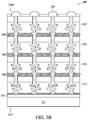
- FIGS. 3A and 3B are schematic drawings illustrating various fabrication stages of the method for preparing the semiconductor package structure in accordance with some embodiments of the present disclosure. It should be understood that similar features in FIGS. 2A to 2H and FIGS. 3A and 3B can include similar materials and similar parameters, and thus descriptions of such details are omitted in the interest of brevity.
- step 102 to step 105 can be performed on the second die 250 .
- a portion of the second die 250 is removed at the second back side 254 B according to step 102 .
- a portion of the substrate 212 is removed such that a portion of the second TSV structure 270 is exposed.
- the portion of the second TSV structure 272 is protruded from the second back side 254 B of the second die 254 B, and thus such portion is referred to as a protrusion 272 .
- a protrusion 270 of the second TSV structure 270 protrudes from the second back side 254 B of the second die 250 after the removal of the portion of the second die 250 .
- a height H of the protrusion 272 of the second TSV structure 270 is between approximately 1 ⁇ m and approximately 5 ⁇ m, but the disclosure is not limited thereto. In some embodiments, the height H of the protrusion 252 of the second TSV structure 270 is approximately 3 ⁇ m, but the disclosure is not limited thereto.
- an organic barrier layer 240 is disposed over the second die 250 at the second back side 244 B, according to step 103 .
- the organic barrier layer 240 is disposed to envelop the protrusion 272 of the second TSV structure 270 .
- An end surface of the protrusion 272 and a top surface of the organic barrier layer 240 are coplanar after the planarization, as shown in FIG. 3A .
- another second die 250 ′ can be provided according to step 104 and bonded to the second die 250 according to step 105 .
- the second die 250 ′ can be a die, a chip or a package. It should be understood that elements of the second die 250 ′ can be similar to those of the first die 210 or the second die 250 , and therefore such details are omitted in the interest of brevity.
- step 102 to step 105 can be repeated to according to product requirements.
- a semiconductor package structure 200 ′ can be formed.
- the semiconductor package structure 200 ′ includes a plurality of dies 210 , 250 , and 250 ′.
- the dies 210 , 250 and 250 ′ are front-to-back bonded.
- the dies 210 , 250 and 250 ′ are bonded to each other by a hybrid bonding structure 280 .
- Steps for forming the hybrid bonding structure 280 can be similar to those described above, and therefore such details are omitted for brevity.
- the semiconductor package structure 200 ′ is obtained.
- the semiconductor package structure 200 ′ can be detached from the carrier substrate 231 after the forming of the conductive member 290 .
- the hybrid bonding structures 280 are formed between each adjacent pair of dies 210 , 250 and 250 ′.
- the dies 210 , 250 and 250 ′ are securely bonded to each other by the forming of the hybrid bonding structures 280 .
- metal diffusion due to surface area difference and/or due to misalignment can be prevented by the organic barrier layer 240 and the inorganic barrier layer 260 of the hybrid bonding structures 280 .
- a method for preparing a semiconductor package structure is provided.
- a first die and a second die are bonded to each other by a hybrid bonding structure.
- the hybrid bonding structure includes an organic layer and an inorganic layer.
- both of the organic and inorganic layers perform a metal diffusion prevention function. Therefore, even if a misalignment issue arises between the first TSV structure of the first die and the bonding pad of the second die, metal diffusion can be prevented by the hybrid bonding structure.
- metal diffusion can be prevented by the hybrid bonding structure.
- the semiconductor package structure includes a first die, a second die and a hybrid bonding structure disposed between the first die and the second die.
- the first die includes a first front side and a first back side opposite to the first front side.
- the second die includes a second front side and a second back side opposite to the second front side.
- the hybrid bonding structure is disposed between the first back side of the first die and the second front side of the second die.
- the first die and the second die are bonded to each other by the hybrid bonding structure.
- the hybrid bonding structure includes an organic barrier layer and an inorganic barrier layer bonded to each other.
- One aspect of the present disclosure provides a method for preparing a semiconductor package structure.
- the method includes the following steps.
- a first die having a first front side, a first back side opposite to the first front side, and a first TSV structure disposed in the first die is provided.
- a portion of the first die at the first back side is removed to expose the first TSV structure.
- An organic barrier layer is disposed over the first back side of the first die.
- a second die having a second front side, a second back side opposite to the second front side, a bonding pad exposed through the second front side, and an inorganic barrier layer disposed over the second front side is provided.
- the organic barrier layer of the first die and the inorganic barrier layer of the second die are bonded, and the first TSV structure of the first die and the bonding pad of the second die are bonded.
Abstract
Description
Claims (17)
Priority Applications (3)
| Application Number | Priority Date | Filing Date | Title |
|---|---|---|---|
| US16/360,619 US10910357B2 (en) | 2019-03-21 | 2019-03-21 | Semiconductor package including hybrid bonding structure and method for preparing the same |
| TW108113782A TWI701796B (en) | 2019-03-21 | 2019-04-19 | Semiconductor package structure and method for preparing the same |
| CN201910429126.3A CN111725147A (en) | 2019-03-21 | 2019-05-22 | Semiconductor packaging structure and preparation method thereof |
Applications Claiming Priority (1)
| Application Number | Priority Date | Filing Date | Title |
|---|---|---|---|
| US16/360,619 US10910357B2 (en) | 2019-03-21 | 2019-03-21 | Semiconductor package including hybrid bonding structure and method for preparing the same |
Publications (2)
| Publication Number | Publication Date |
|---|---|
| US20200303361A1 US20200303361A1 (en) | 2020-09-24 |
| US10910357B2 true US10910357B2 (en) | 2021-02-02 |
Family
ID=72513979
Family Applications (1)
| Application Number | Title | Priority Date | Filing Date |
|---|---|---|---|
| US16/360,619 Active US10910357B2 (en) | 2019-03-21 | 2019-03-21 | Semiconductor package including hybrid bonding structure and method for preparing the same |
Country Status (3)
| Country | Link |
|---|---|
| US (1) | US10910357B2 (en) |
| CN (1) | CN111725147A (en) |
| TW (1) | TWI701796B (en) |
Cited By (1)
| Publication number | Priority date | Publication date | Assignee | Title |
|---|---|---|---|---|
| US20210057368A1 (en) * | 2017-07-21 | 2021-02-25 | United Microelectronics Corp. | Chip-stack structure |
Families Citing this family (9)
| Publication number | Priority date | Publication date | Assignee | Title |
|---|---|---|---|---|
| US10903142B2 (en) * | 2018-07-31 | 2021-01-26 | Intel Corporation | Micro through-silicon via for transistor density scaling |
| US11417628B2 (en) | 2018-12-26 | 2022-08-16 | Ap Memory Technology Corporation | Method for manufacturing semiconductor structure |
| US11189563B2 (en) * | 2019-08-01 | 2021-11-30 | Nanya Technology Corporation | Semiconductor structure and manufacturing method thereof |
| US11410929B2 (en) * | 2019-09-17 | 2022-08-09 | Taiwan Semiconductor Manufacturing Co., Ltd. | Semiconductor device and method of manufacture |
| US11239238B2 (en) | 2019-10-29 | 2022-02-01 | Intel Corporation | Thin film transistor based memory cells on both sides of a layer of logic devices |
| CN112236858B (en) * | 2020-09-02 | 2024-04-05 | 长江存储科技有限责任公司 | Pad lead-out structure for Xbonding architecture |
| US11817442B2 (en) * | 2020-12-08 | 2023-11-14 | Intel Corporation | Hybrid manufacturing for integrated circuit devices and assemblies |
| US11756886B2 (en) | 2020-12-08 | 2023-09-12 | Intel Corporation | Hybrid manufacturing of microeletronic assemblies with first and second integrated circuit structures |
| CN113510538A (en) * | 2021-06-23 | 2021-10-19 | 闳康技术检测(上海)有限公司 | Multilayer RDL (refuse derived fuel) delaminating process |
Citations (6)
| Publication number | Priority date | Publication date | Assignee | Title |
|---|---|---|---|---|
| US20110026232A1 (en) * | 2009-07-30 | 2011-02-03 | Megica Corporation | System-in packages |
| TW201320298A (en) | 2011-10-07 | 2013-05-16 | Freescale Semiconductor Inc | Stacked semiconductor devices |
| US20130154112A1 (en) * | 2011-12-16 | 2013-06-20 | Katholieke Universiteit Leuven, K.U. Leuven R&D | Method for Forming Isolation Trenches in Micro-Bump Interconnect Structures and Devices Obtained Thereof |
| TW201413913A (en) | 2012-09-28 | 2014-04-01 | Taiwan Semiconductor Mfg Co Ltd | Semiconductor package and method for manufacturing the same |
| TW201519383A (en) | 2013-11-07 | 2015-05-16 | Sk Hynix Inc | Semiconductor devices, methods of manufacturing the same, memory cards including the same and electronic systems including the same |
| US20200111763A1 (en) * | 2018-10-04 | 2020-04-09 | Samsung Electronics Co., Ltd. | Semiconductor package |
Family Cites Families (3)
| Publication number | Priority date | Publication date | Assignee | Title |
|---|---|---|---|---|
| US8159060B2 (en) * | 2009-10-29 | 2012-04-17 | International Business Machines Corporation | Hybrid bonding interface for 3-dimensional chip integration |
| US9142517B2 (en) * | 2012-06-05 | 2015-09-22 | Taiwan Semiconductor Manufacturing Company, Ltd. | Hybrid bonding mechanisms for semiconductor wafers |
| US10163864B1 (en) * | 2017-08-16 | 2018-12-25 | Globalfoundries Inc. | Vertically stacked wafers and methods of forming same |
-
2019
- 2019-03-21 US US16/360,619 patent/US10910357B2/en active Active
- 2019-04-19 TW TW108113782A patent/TWI701796B/en active
- 2019-05-22 CN CN201910429126.3A patent/CN111725147A/en active Pending
Patent Citations (6)
| Publication number | Priority date | Publication date | Assignee | Title |
|---|---|---|---|---|
| US20110026232A1 (en) * | 2009-07-30 | 2011-02-03 | Megica Corporation | System-in packages |
| TW201320298A (en) | 2011-10-07 | 2013-05-16 | Freescale Semiconductor Inc | Stacked semiconductor devices |
| US20130154112A1 (en) * | 2011-12-16 | 2013-06-20 | Katholieke Universiteit Leuven, K.U. Leuven R&D | Method for Forming Isolation Trenches in Micro-Bump Interconnect Structures and Devices Obtained Thereof |
| TW201413913A (en) | 2012-09-28 | 2014-04-01 | Taiwan Semiconductor Mfg Co Ltd | Semiconductor package and method for manufacturing the same |
| TW201519383A (en) | 2013-11-07 | 2015-05-16 | Sk Hynix Inc | Semiconductor devices, methods of manufacturing the same, memory cards including the same and electronic systems including the same |
| US20200111763A1 (en) * | 2018-10-04 | 2020-04-09 | Samsung Electronics Co., Ltd. | Semiconductor package |
Non-Patent Citations (1)
| Title |
|---|
| An Office Action from the corresponding Taiwanese application, dated Nov. 18, 2019. |
Cited By (1)
| Publication number | Priority date | Publication date | Assignee | Title |
|---|---|---|---|---|
| US20210057368A1 (en) * | 2017-07-21 | 2021-02-25 | United Microelectronics Corp. | Chip-stack structure |
Also Published As
| Publication number | Publication date |
|---|---|
| TW202036831A (en) | 2020-10-01 |
| TWI701796B (en) | 2020-08-11 |
| US20200303361A1 (en) | 2020-09-24 |
| CN111725147A (en) | 2020-09-29 |
Similar Documents
| Publication | Publication Date | Title |
|---|---|---|
| US10910357B2 (en) | Semiconductor package including hybrid bonding structure and method for preparing the same | |
| US11935802B2 (en) | Integrated circuit package and method of forming same | |
| US9240349B2 (en) | Interconnect structures for substrate | |
| US11855046B2 (en) | Memory packages and methods of forming same | |
| US11139249B2 (en) | Semiconductor devices and methods of forming the same | |
| US11862605B2 (en) | Integrated circuit package and method of forming same | |
| US20240087987A1 (en) | Front end of line interconnect structures and associated systems and methods | |
| US11658069B2 (en) | Method for manufacturing a semiconductor device having an interconnect structure over a substrate | |
| TWI744071B (en) | Integrated circuit device and packaging method for integrated circuit device | |
| US20220375793A1 (en) | Semiconductor Device and Method | |
| US11810793B2 (en) | Semiconductor packages and methods of forming same | |
| US20230260941A1 (en) | Semiconductor Device and Method | |
| US20220068820A1 (en) | Front end of line interconnect structures and associated systems and methods | |
| US10763199B2 (en) | Semiconductor package structure and method for preparing the same | |
| US20240063151A1 (en) | Semiconductor structure having conductive pad with protrusion and manufacturing method thereof | |
| US20240079364A1 (en) | Die Structures and Methods of Forming the Same | |
| TWI758129B (en) | Semiconductor packages | |
| US11798908B2 (en) | Trilayer bonding bump structure for semiconductor package | |
| US11955423B2 (en) | Semiconductor device and method | |
| CN117316924A (en) | Die structure and method of forming the same |
Legal Events
| Date | Code | Title | Description |
|---|---|---|---|
| FEPP | Fee payment procedure |
Free format text: ENTITY STATUS SET TO UNDISCOUNTED (ORIGINAL EVENT CODE: BIG.); ENTITY STATUS OF PATENT OWNER: LARGE ENTITY |
|
| AS | Assignment |
Owner name: NANYA TECHNOLOGY CORPORATION, TAIWAN Free format text: ASSIGNMENT OF ASSIGNORS INTEREST;ASSIGNOR:SHIH, SHING-YIH;REEL/FRAME:048887/0414 Effective date: 20190214 |
|
| STPP | Information on status: patent application and granting procedure in general |
Free format text: NOTICE OF ALLOWANCE MAILED -- APPLICATION RECEIVED IN OFFICE OF PUBLICATIONS |
|
| STPP | Information on status: patent application and granting procedure in general |
Free format text: PUBLICATIONS -- ISSUE FEE PAYMENT VERIFIED |
|
| STCF | Information on status: patent grant |
Free format text: PATENTED CASE |