US10910236B2 - Semiconductor manufacturing apparatus and method of manufacturing semiconductor device - Google Patents
Semiconductor manufacturing apparatus and method of manufacturing semiconductor device Download PDFInfo
- Publication number
- US10910236B2 US10910236B2 US16/294,978 US201916294978A US10910236B2 US 10910236 B2 US10910236 B2 US 10910236B2 US 201916294978 A US201916294978 A US 201916294978A US 10910236 B2 US10910236 B2 US 10910236B2
- Authority
- US
- United States
- Prior art keywords
- liquid
- channel
- film
- amount
- supplementing
- Prior art date
- Legal status (The legal status is an assumption and is not a legal conclusion. Google has not performed a legal analysis and makes no representation as to the accuracy of the status listed.)
- Active, expires
Links
- 239000004065 semiconductor Substances 0.000 title claims abstract description 37
- 238000004519 manufacturing process Methods 0.000 title claims abstract description 31
- 239000007788 liquid Substances 0.000 claims abstract description 121
- 230000001502 supplementing effect Effects 0.000 claims abstract description 44
- 239000000758 substrate Substances 0.000 claims abstract description 16
- 239000000126 substance Substances 0.000 claims abstract description 12
- 238000005530 etching Methods 0.000 claims description 110
- 239000012212 insulator Substances 0.000 claims description 13
- 239000013589 supplement Substances 0.000 claims description 5
- XUIMIQQOPSSXEZ-UHFFFAOYSA-N Silicon Chemical compound [Si] XUIMIQQOPSSXEZ-UHFFFAOYSA-N 0.000 claims description 4
- 238000000034 method Methods 0.000 claims description 4
- 229910052710 silicon Inorganic materials 0.000 claims description 4
- 239000010703 silicon Substances 0.000 claims description 4
- 238000004891 communication Methods 0.000 claims description 3
- 238000007599 discharging Methods 0.000 claims 4
- 238000010438 heat treatment Methods 0.000 claims 1
- 239000000243 solution Substances 0.000 description 85
- VYPSYNLAJGMNEJ-UHFFFAOYSA-N Silicium dioxide Chemical compound O=[Si]=O VYPSYNLAJGMNEJ-UHFFFAOYSA-N 0.000 description 74
- 239000000377 silicon dioxide Substances 0.000 description 34
- 229910052581 Si3N4 Inorganic materials 0.000 description 30
- HQVNEWCFYHHQES-UHFFFAOYSA-N silicon nitride Chemical compound N12[Si]34N5[Si]62N3[Si]51N64 HQVNEWCFYHHQES-UHFFFAOYSA-N 0.000 description 30
- 239000010410 layer Substances 0.000 description 28
- 238000011084 recovery Methods 0.000 description 24
- NBIIXXVUZAFLBC-UHFFFAOYSA-N Phosphoric acid Chemical compound OP(O)(O)=O NBIIXXVUZAFLBC-UHFFFAOYSA-N 0.000 description 10
- 239000011229 interlayer Substances 0.000 description 6
- 229910052814 silicon oxide Inorganic materials 0.000 description 6
- 229910000147 aluminium phosphate Inorganic materials 0.000 description 5
- 239000007864 aqueous solution Substances 0.000 description 5
- 238000001556 precipitation Methods 0.000 description 5
- 230000007423 decrease Effects 0.000 description 3
- 238000010586 diagram Methods 0.000 description 2
- 238000009434 installation Methods 0.000 description 2
- 230000000149 penetrating effect Effects 0.000 description 2
- 230000001376 precipitating effect Effects 0.000 description 2
- 230000000630 rising effect Effects 0.000 description 2
- 238000012986 modification Methods 0.000 description 1
- 230000004048 modification Effects 0.000 description 1
- 229910021420 polycrystalline silicon Inorganic materials 0.000 description 1
- 229920005591 polysilicon Polymers 0.000 description 1
- 238000005070 sampling Methods 0.000 description 1
- 238000006467 substitution reaction Methods 0.000 description 1
- 230000009469 supplementation Effects 0.000 description 1
- WFKWXMTUELFFGS-UHFFFAOYSA-N tungsten Chemical compound [W] WFKWXMTUELFFGS-UHFFFAOYSA-N 0.000 description 1
- 229910052721 tungsten Inorganic materials 0.000 description 1
- 239000010937 tungsten Substances 0.000 description 1
Images


Classifications
-
- H—ELECTRICITY
- H01—ELECTRIC ELEMENTS
- H01L—SEMICONDUCTOR DEVICES NOT COVERED BY CLASS H10
- H01L21/00—Processes or apparatus adapted for the manufacture or treatment of semiconductor or solid state devices or of parts thereof
- H01L21/67—Apparatus specially adapted for handling semiconductor or electric solid state devices during manufacture or treatment thereof; Apparatus specially adapted for handling wafers during manufacture or treatment of semiconductor or electric solid state devices or components ; Apparatus not specifically provided for elsewhere
- H01L21/67005—Apparatus not specifically provided for elsewhere
- H01L21/67011—Apparatus for manufacture or treatment
- H01L21/67017—Apparatus for fluid treatment
- H01L21/67063—Apparatus for fluid treatment for etching
- H01L21/67075—Apparatus for fluid treatment for etching for wet etching
- H01L21/6708—Apparatus for fluid treatment for etching for wet etching using mainly spraying means, e.g. nozzles
-
- H—ELECTRICITY
- H01—ELECTRIC ELEMENTS
- H01L—SEMICONDUCTOR DEVICES NOT COVERED BY CLASS H10
- H01L21/00—Processes or apparatus adapted for the manufacture or treatment of semiconductor or solid state devices or of parts thereof
- H01L21/02—Manufacture or treatment of semiconductor devices or of parts thereof
- H01L21/04—Manufacture or treatment of semiconductor devices or of parts thereof the devices having potential barriers, e.g. a PN junction, depletion layer or carrier concentration layer
- H01L21/18—Manufacture or treatment of semiconductor devices or of parts thereof the devices having potential barriers, e.g. a PN junction, depletion layer or carrier concentration layer the devices having semiconductor bodies comprising elements of Group IV of the Periodic Table or AIIIBV compounds with or without impurities, e.g. doping materials
- H01L21/30—Treatment of semiconductor bodies using processes or apparatus not provided for in groups H01L21/20 - H01L21/26
- H01L21/302—Treatment of semiconductor bodies using processes or apparatus not provided for in groups H01L21/20 - H01L21/26 to change their surface-physical characteristics or shape, e.g. etching, polishing, cutting
- H01L21/306—Chemical or electrical treatment, e.g. electrolytic etching
- H01L21/30604—Chemical etching
-
- H—ELECTRICITY
- H01—ELECTRIC ELEMENTS
- H01L—SEMICONDUCTOR DEVICES NOT COVERED BY CLASS H10
- H01L21/00—Processes or apparatus adapted for the manufacture or treatment of semiconductor or solid state devices or of parts thereof
- H01L21/67—Apparatus specially adapted for handling semiconductor or electric solid state devices during manufacture or treatment thereof; Apparatus specially adapted for handling wafers during manufacture or treatment of semiconductor or electric solid state devices or components ; Apparatus not specifically provided for elsewhere
- H01L21/67005—Apparatus not specifically provided for elsewhere
- H01L21/67011—Apparatus for manufacture or treatment
- H01L21/67017—Apparatus for fluid treatment
-
- H—ELECTRICITY
- H01—ELECTRIC ELEMENTS
- H01L—SEMICONDUCTOR DEVICES NOT COVERED BY CLASS H10
- H01L21/00—Processes or apparatus adapted for the manufacture or treatment of semiconductor or solid state devices or of parts thereof
- H01L21/67—Apparatus specially adapted for handling semiconductor or electric solid state devices during manufacture or treatment thereof; Apparatus specially adapted for handling wafers during manufacture or treatment of semiconductor or electric solid state devices or components ; Apparatus not specifically provided for elsewhere
- H01L21/67005—Apparatus not specifically provided for elsewhere
- H01L21/67242—Apparatus for monitoring, sorting or marking
- H01L21/67248—Temperature monitoring
-
- H—ELECTRICITY
- H01—ELECTRIC ELEMENTS
- H01L—SEMICONDUCTOR DEVICES NOT COVERED BY CLASS H10
- H01L21/00—Processes or apparatus adapted for the manufacture or treatment of semiconductor or solid state devices or of parts thereof
- H01L21/67—Apparatus specially adapted for handling semiconductor or electric solid state devices during manufacture or treatment thereof; Apparatus specially adapted for handling wafers during manufacture or treatment of semiconductor or electric solid state devices or components ; Apparatus not specifically provided for elsewhere
- H01L21/67005—Apparatus not specifically provided for elsewhere
- H01L21/67242—Apparatus for monitoring, sorting or marking
- H01L21/67253—Process monitoring, e.g. flow or thickness monitoring
Definitions
- Embodiments described herein relate to a semiconductor manufacturing apparatus and a method of manufacturing a semiconductor device.
- silica dissolves from the silicon nitride film in the phosphoric acid aqueous solution. In this case, precipitation of silica needs to be prevented. However, it is undesirable to frequently replace the phosphoric acid aqueous solution to prevent the precipitation of the silica. The same applies to the cases of treating films other than the silicon nitride film and the cases of using liquids other than the phosphoric acid aqueous solution.
- FIG. 1 is a schematic diagram illustrating a configuration of a semiconductor manufacturing apparatus of a first embodiment
- FIG. 2 is a graph for explaining operations of the semiconductor manufacturing apparatus of the first embodiment
- FIGS. 3A and 3B are other graphs for explaining the operations of the semiconductor manufacturing apparatus of the first embodiment
- FIGS. 4A to 4D are other graphs for explaining the operations of the semiconductor manufacturing apparatus of the first embodiment
- FIG. 5 is another graph for explaining the operations of the semiconductor manufacturing apparatus of the first embodiment.
- FIGS. 6A to 7B are cross-sectional views illustrating a method of manufacturing a semiconductor device of the first embodiment.
- a semiconductor manufacturing apparatus includes a liquid supplier configured to supply liquid to a film on a substrate and cause a substance to dissolve from the film in the liquid.
- the apparatus further includes a first channel configured to recover the liquid supplied to the film and feed the liquid again to the liquid supplier, and a second channel configured to drain the liquid supplied to the film.
- the apparatus further includes a first switching module configured to switch a discharge destination of the liquid supplied to the film between the first channel and the second channel, and a second switching module configured to switch between supplementing and not supplementing the first channel with new liquid.
- the apparatus further includes a controller configured to control the first and second switching modules to adjust concentration of the substance in the liquid to be supplied to the film.
- FIG. 1 is a schematic diagram illustrating a configuration of a semiconductor manufacturing apparatus of a first embodiment.
- the semiconductor manufacturing apparatus of FIG. 1 is a single wafer etching apparatus that treats a wafer 1 by an etching solution.
- the semiconductor manufacturing apparatus of FIG. 1 includes a treatment chamber 11 including a recovery cup 11 a , a rotary shaft 11 b , and a nozzle 11 c .
- the semiconductor manufacturing apparatus further includes a temperature adjustment tank 12 , a first pump 13 , a second pump 14 , a heater 15 , a supplementary valve 16 , and a controller 17 including a cup controller 17 a and a valve controller 17 b .
- the recovery cup 11 a is an example of the first switching module
- the supplementary valve 16 is an example of the second switching module.
- the nozzle 11 c is an example of the liquid supplier
- the temperature adjustment tank 12 is an example of a liquid tank.
- FIG. 1 further illustrates channels L 1 to L 5 for an etching solution.
- the channels L 1 , L 2 are examples of the first channel, and the channel L 3 is an example of the second channel.
- the treatment chamber 11 contains the wafer 1 and treats the wafer 1 by an etching solution.
- FIG. 1 illustrates X- and Y-directions perpendicular to each other and parallel to an installation surface of the treatment chamber 11 , and a Z-direction perpendicular to the installation surface of the treatment chamber 11 .
- the positive Z-direction is regarded as an upward direction
- the negative Z-direction is regarded as a downward direction.
- the negative Z-direction may or may not coincide with the gravitational direction.
- the rotary shaft 11 b supports and rotates the wafer 1 .
- the wafer 1 includes a silicon substrate, which is an example of the substrate, and a silicon nitride film, which is an example of the film, provided on the substrate.
- the nozzle 11 c supplies the etching solution from the channel L 1 to this silicon nitride film.
- the silicon nitride film is etched by the etching solution, and silica dissolves from the silicon nitride film in the etching solution.
- the etching solution of the present embodiment is a phosphoric acid aqueous solution, for example.
- the recovery cup 11 a is movable in the upward and downward directions relative to the wafer 1 .
- the etching solution supplied to the silicon nitride film is discharged into the channel L 2 through a channel inside the recovery cup 11 a , as indicated by the arrow P 1 .
- the recovery cup 11 a is at a low position, the etching solution supplied to the silicon nitride film is discharged into the channel L 3 through a channel inside the recovery cup 11 a , as indicated by the arrow P 2 .
- the recovery cup 11 a can switch a discharge destination of the etching solution supplied to the silicon nitride film between the channel L 2 and the channel L 3 .
- the channel L 1 and the channel L 2 form a circulation channel for circulation of the etching solution between the treatment chamber 11 and the temperature adjustment tank 12 .
- the temperature adjustment tank 12 and the first pump 13 are provided in this circulation channel.
- the temperature adjustment tank 12 reserves the etching solution, and the first pump 13 feeds the etching solution from the temperature adjustment tank 12 to the nozzle 11 c.
- the channel L 2 recovers the etching solution discharged from the treatment chamber 11 (the arrow P 1 ) into the temperature adjustment tank 12 . As a result, the etching solution is fed to the nozzle 11 c again through the channel L 1 .
- the channel L 3 drains the etching solution discharged from the treatment chamber 11 (the arrow P 2 ) out of the semiconductor manufacturing apparatus. Accordingly, the recovery cup 11 a can switch between recovering and draining the etching solution.
- the channel L 4 forms a circulation channel for circulation of the etching solution between the temperature adjustment tank 12 and the heater 15 .
- the heater 15 and the second pump 14 are provided in this circulation channel.
- the heater 15 heats the etching solution discharged from the temperature adjustment tank 12 into the channel L 4 .
- the etching solution heated by the heater 15 is returned to the temperature adjustment tank 12 by the second pump 14 through the channel L 4 . This adjusts a temperature of the etching solution flowing in the channel L 1 and the channel L 2 to a predetermined temperature.
- the channel L 5 is used for supplementing the temperature adjustment tank 12 with the etching solution (new etching solution).
- the supplementary valve 16 is provided in the channel L 5 and used for switching between supplementing and not supplementing the temperature adjustment tank 12 with the new etching solution.
- the amount of etching solution circulating in the channels L 1 , L 2 of the present embodiment can be reduced by drainage to the channel L 3 and increased by supplementation from the channel L 5 .
- the controller 17 controls operations of the semiconductor manufacturing apparatus.
- Examples of the controller 17 include a processor, an electric circuit and a personal computer (PC).
- the controller 17 causes the cup controller 17 a to control lift-up operation and lift-down operation of the recovery cup 11 a , whereby the recovering amount and the draining mount of the etching solution is adjusted.
- the controller 17 causes the valve controller 17 b to control opening and closing and degree of opening of the supplementary valve 16 , whereby the supplementing amount of the etching solution is adjusted.
- the controller 17 of the present embodiment controls operations of the recovery cup 11 a and the supplementary valve 16 to adjust concentration of silica in the etching solution to be supplied to the silicon nitride film. This adjustment of the silica concentration will be described in detail below.
- FIG. 2 is a graph for explaining operations of the semiconductor manufacturing apparatus of the first embodiment.
- FIG. 2 shows changes in the silica concentration from the start of etching of the aforementioned silicon nitride film if the recovery of the etching solution is continued without draining or supplementing the etching solution.
- the vertical axis of FIG. 2 represents the silica concentration in the etching solution.
- the horizontal axis of FIG. 2 represents etching time during which the silicon nitride film has been treated with the etching solution. The etching time indicates a lapse of time from the start of etching.
- the silica concentration increases from an initial concentration (here, 55 ppm).
- the silica concentration then exceeds a precipitating concentration (here, 65 ppm), at which silica in the etching solution starts to be precipitated.
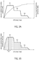
- FIGS. 3A and 3B are other graphs for explaining the operations of the semiconductor manufacturing apparatus of the first embodiment.
- FIG. 3A shows changes in a liquid contacting area and the silica concentration from the start of etching of the aforementioned silicon nitride film if the recovery of the etching solution is continued without draining or supplementing the etching solution as in FIG. 2 .
- the liquid contacting area refers to an area where the silicon nitride film contacts the etching solution at each time point.
- FIG. 3A exemplarily shows the case where the liquid contacting area decreases from S 1 to S 2 and from S 2 to S 3 with the lapse of the etching time.
- the liquid contacting area is S 1
- the etching amount of the silicon nitride film is large, which results in the silica concentration sharply rising.
- the liquid contacting area is S 3
- the etching amount of the silicon nitride film is small, which results in the silica concentration slowly rising.
- FIG. 3B shows sampled values of the liquid contacting area shown in FIG. 3A .
- FIG. 3B is a bar graph plotting sampled values that are obtained by sampling values of the liquid contacting area for each predetermined time “At”.
- the controller 17 of the present embodiment controls operations of the recovery cup 11 a and the supplementary valve 16 based on these sampled values.
- FIGS. 4A to 4D are other graphs for explaining the operations of the semiconductor manufacturing apparatus of the first embodiment.
- FIG. 4A exemplarily shows three sampled values K 1 to K 3 .
- the sampled value K 1 represents a small liquid contacting area
- the sampled value K 2 represents a medium liquid contacting area
- the sampled value K 3 represents a large liquid contacting area.
- FIG. 4B , FIG. 4C and FIG. 4D respectively show operations of the nozzle 11 c , the recovery cup 11 a and the supplementary valve 16 at each of the three sampled values K 1 to K 3 .
- the nozzle 11 c is always open, continuing to discharge the etching solution to the silicon nitride film.
- the recovery cup 11 a and the supplementary valve 16 alternately and repeatedly recovers the etching solution and drains and supplements the etching solution, as shown in FIGS. 4C and 4D .
- Reference numerals A 1 to A 3 each denote a period in which the etching solution is recovered, and reference numerals B 1 to B 3 each denote a period in which the etching solution is drained and supplemented.
- the supplementary valve 16 is closed to stop supplementing the temperature adjustment tank 12 with the etching solution.
- the supplementary valve 16 is opened to supplement the temperature adjustment tank 12 with the etching solution.
- the etching solution is entirely recovered with no etching solution being drained or supplemented. Accordingly, in the former period, the amount of etching solution circulating in the channels L 1 , L 2 is constant. On the other hand, in the latter period, the etching solution is not recovered at all, but the etching solution is drained and supplemented. At this time, in the present embodiment, the draining amount of the etching solution is made equal to the supplementing amount of the etching solution. Accordingly, in the latter period too, the amount of etching solution circulating in the channels L 1 , L 2 is constant.
- a length ratio of the former period to the latter period is varied according to the sampled values.
- the ratio is set to A 1 :B 1 .
- the ratio is set to A 2 : 62 .
- the ratio is set to A 3 :B 3 .
- the period B 3 is set longer to increase the draining amount and the supplementing amount of the etching solution. This allows to prevent an increase in the silica concentration despite a large amount of silica dissolving from the silicon nitride film.
- the period B 1 is set shorter to reduce the draining amount and the supplementing amount of the etching solution. This allows to prevent an increase in the silica concentration while economizing the etching solution.
- the controller 17 of the present embodiment controls operations of the recovery cup 11 a and the supplementary valve 16 to adjust the recovering amount, the draining amount and the supplementing amount of the etching solution per unit time and to adjust the silica concentration. This allows for an efficient use of the etching solution according to the liquid contacting area.
- the ratio of A 1 :B 1 is set to 2:1 when the sampled value is K 1 and the ratio of A 3 :B 3 is set to 1:2 when the sampled value is K 3 .
- the supplementing period of the etching solution is twice than when the sampled value is K 1 .
- the supplementing amount of the etching solution per unit time is twice than when the sampled value is K 1 .
- the controller 17 of the present embodiment controls operations of the recovery cup 11 a and the supplementary valve 16 such that the recovering amount, the draining amount and the supplementing amount of the etching solution per unit time is varied according to the liquid contacting area.
- FIG. 5 is another graph for explaining the operations of the semiconductor manufacturing apparatus of the first embodiment.
- the controller 17 of the present embodiment controls the recovery cup 11 a and the supplementary valve 16 such that an increase in the silica concentration is prevented. Specifically, the controller 17 controls the recovery cup 11 a and the supplementary valve 16 such that the silica concentration is maintained at a predetermined concentration (here, the initial concentration), as shown in FIG. 5 . Since the control may involve errors, the control in the present embodiment is performed such that the silica concentration is maintained within a range of ⁇ 5 ppm from the predetermined concentration, namely within a range from 50 ppm to 60 ppm.
- the controller 17 obtains information representing a relationship between the etching time and the liquid contacting area as a recipe before starting the etching. This information may be read from a storage device inside the semiconductor manufacturing apparatus, or may be received from outside of the semiconductor manufacturing apparatus through communication processing.
- the controller 17 adjusts the recovering amount, the draining amount and the supplementing amount of the etching solution at given etching time based on the liquid contacting area at that given etching time.
- the liquid contacting area at that given etching time can be identified from the above information representing the relationship between the etching time and the liquid contacting area. This adjustment is made for each time “At” using the sampled values of the liquid contacting area.
- the recovering period of the etching solution is set to A 1 and the draining and supplementing periods of the etching solution are set to B 1 , during etching time from “t” to “t”+“ ⁇ t”.
- the recovering period is set to A 2
- the draining and supplementing periods are set to B 2 .
- the recovering period is set to A 3
- the draining and supplementing periods are set to B 3 .
- the semiconductor manufacturing apparatus of the present embodiment may include a measuring instrument to measure the liquid contacting area of the silicon nitride film.
- the controller 17 may set the recovering period, the draining period and the supplementing period at each time point based on the measured liquid contacting area. This allows to maintain the silica concentration at the predetermined concentration, similarly to the above case of using the recipe.
- the controller 17 of the present embodiment adjusts the silica concentration within the lower limit (50 ppm) and the upper limit (60 ppm) to maintain the silica concentration at the predetermined concentration (55 ppm).
- the upper and lower limits are not limited to these values.
- the upper limit of 60 ppm is set to take a margin of 5 ppm from the precipitating concentration (65 ppm).
- the lower limit of 50 ppm is set to prevent an excessive etching of the silicon nitride film due to too much reduction in the silica concentration.
- FIGS. 6A to 7B are cross-sectional views illustrating a method of manufacturing a semiconductor device of the first embodiment.
- the semiconductor device is a three-dimensional semiconductor memory.
- FIG. 6A illustrates a substrate 21 , a base layer 22 , plural first insulating layers 23 , plural second insulating layers 24 and an inter layer dielectric 25 .
- the substrate 21 is, for example, a semiconductor substrate such as a silicon substrate.
- the base layer 22 includes a first base layer 22 a , a second base layer 22 b , a third base layer 22 c and an inter layer dielectric 22 d sequentially formed on the substrate 21 .
- the inter layer dielectric 22 d is, for example, a silicon oxide film.
- the plural first insulating layers 23 and the plural second insulating layers 24 are alternately formed on the inter layer dielectric 22 d .
- the first insulating layer 23 is, for example, a silicon oxide film.
- the second insulating layer 24 is, for example, a silicon nitride film.
- the inter layer dielectric 25 is formed on these first and second insulating layers 23 , 24 .
- the inter layer dielectric 25 is, for example, a silicon oxide film.
- FIG. 6A illustrates the state where a shallow trench ST penetrating the first and second insulating layers 23 , 24 and the like is formed and a cover insulator 26 is formed on the sides and bottom of the shallow trench ST.
- the cover insulator 26 is, for example, a silicon nitride film.
- FIG. 6A further illustrates a memory insulator 27 , a channel semiconductor layer 28 and a core insulator 29 sequentially formed in each memory hole MH penetrating the first and second insulating layers 23 , 24 and the like.
- the memory insulator 27 includes a block insulator 27 a such as a silicon oxide film, a charge storage layer 27 b such as a silicon nitride film, and a tunnel insulator 27 c such as a silicon oxide film.
- the channel semiconductor layer 28 is, for example, a polysilicon layer
- the core insulator 29 is, for example, a silicon oxide film.
- the plural second insulating layers 24 and the cover insulator 26 are the silicon nitride films to be treated by the etching solution. Treatment of these silicon nitride films is performed by the semiconductor manufacturing apparatus of FIG. 1 . Details of this treatment will be explained with reference to FIGS. 6B to 7B .
- the cover insulator 26 is removed by the etching solution ( FIG. 6B ).
- the liquid contacting area is S 1 shown in FIG. 3B .
- the liquid contacting area S 1 equals areas of the sides and bottom of the shallow trench ST, occupying a large area.
- the plural second insulating layers 24 start to be removed by the etching solution ( FIG. 7A ).
- the liquid contacting area is S 2 shown in FIG. 3B .
- the liquid contacting area S 2 equals areas of the sides of these second insulating layers 24 , becoming smaller than the liquid contacting area S 1 .
- the second insulating layers 24 continue to be removed by the etching solution after the etching solution reaches the memory insulators 27 ( FIG. 7B ).
- the liquid contacting area is S 3 shown in FIG. 3B .
- the liquid contacting area S 3 equals that obtained by subtracting areas of the sides of the memory insulators 27 from the areas of the sides of the second insulating layers 24 , becoming smaller than the liquid contacting area S 2 .
- the liquid contacting area decreases as the etching proceeds. Accordingly, with the decrease in the liquid contacting area, the controller 17 shortens the draining and supplementing periods of the etching solution. This allows for an efficient use of the etching solution according to the liquid contacting area.
- an electrode layer such as a tungsten layer is formed within each cavity produced by removing the second insulating layers 24 .
- an electrode layer such as a tungsten layer is formed within each cavity produced by removing the second insulating layers 24 .
- the controller 17 of the present embodiment controls the recovery cup 11 a and the supplementary valve 16 to adjust the silica concentration in the etching solution to be supplied to the silicon nitride film on the substrate. Therefore, the present embodiment allows for an efficient use of the etching solution such as by preventing precipitation of silica and wasteful use of the etching solution.
- the semiconductor manufacturing apparatus of the present embodiment is a single wafer apparatus; however, the semiconductor manufacturing apparatus may be a batch type apparatus.
- the recovery cup 11 a of the present embodiment may be replaced with any other component that switches between recovering and draining the etching solution (e.g. a valve).
- the supplementary valve 16 of the present embodiment may be replaced with any other component that switches between supplementing and not supplementing the etching solution.
- K 1 to K 3 as examples of the sampled values of the liquid contacting area, the number of kinds of the sampled values are not limited to three.
Landscapes
- Engineering & Computer Science (AREA)
- Physics & Mathematics (AREA)
- Condensed Matter Physics & Semiconductors (AREA)
- General Physics & Mathematics (AREA)
- Manufacturing & Machinery (AREA)
- Computer Hardware Design (AREA)
- Microelectronics & Electronic Packaging (AREA)
- Power Engineering (AREA)
- Chemical & Material Sciences (AREA)
- Chemical Kinetics & Catalysis (AREA)
- General Chemical & Material Sciences (AREA)
- Weting (AREA)
Abstract
Description
Claims (6)
Applications Claiming Priority (2)
| Application Number | Priority Date | Filing Date | Title |
|---|---|---|---|
| JP2018171342A JP7096112B2 (en) | 2018-09-13 | 2018-09-13 | Semiconductor manufacturing equipment and methods for manufacturing semiconductor equipment |
| JP2018-171342 | 2018-09-13 |
Publications (2)
| Publication Number | Publication Date |
|---|---|
| US20200090960A1 US20200090960A1 (en) | 2020-03-19 |
| US10910236B2 true US10910236B2 (en) | 2021-02-02 |
Family
ID=69772249
Family Applications (1)
| Application Number | Title | Priority Date | Filing Date |
|---|---|---|---|
| US16/294,978 Active 2039-04-29 US10910236B2 (en) | 2018-09-13 | 2019-03-07 | Semiconductor manufacturing apparatus and method of manufacturing semiconductor device |
Country Status (2)
| Country | Link |
|---|---|
| US (1) | US10910236B2 (en) |
| JP (1) | JP7096112B2 (en) |
Citations (12)
| Publication number | Priority date | Publication date | Assignee | Title |
|---|---|---|---|---|
| US20030180471A1 (en) * | 2002-03-19 | 2003-09-25 | Tokyo Electron Limited | Process liquid supply mechanism and process liquid supply method |
| JP2005530605A (en) | 2002-06-25 | 2005-10-13 | エスイーゼツト・アクチエンゲゼルシヤフト | Apparatus for liquid treatment of disk-like objects |
| US20120260946A1 (en) * | 2011-04-18 | 2012-10-18 | Nobuhiro Ogata | Liquid processing apparatus, liquid processing method, and computer-readable recording medium having program stored therein |
| US20150093906A1 (en) | 2013-09-30 | 2015-04-02 | Shibaura Mechatronics Corporation | Substrate treatment method and substrate treatment apparatus |
| US20170338131A1 (en) * | 2016-05-18 | 2017-11-23 | SCREEN Holdings Co., Ltd. | Substrate processing apparatus and substrate processing method |
| JP2017216478A (en) | 2013-09-30 | 2017-12-07 | 芝浦メカトロニクス株式会社 | Substrate processing device |
| JP2018006623A (en) | 2016-07-05 | 2018-01-11 | 東京エレクトロン株式会社 | Substrate liquid processing apparatus, substrate liquid processing method, and storage medium |
| US20180197756A1 (en) * | 2015-08-18 | 2018-07-12 | SCREEN Holdings Co., Ltd. | Substrate processing apparatus and substrate processing method |
| US20180226277A1 (en) * | 2017-02-09 | 2018-08-09 | Tokyo Electron Limited | Liquid processing apparatus |
| US20180277398A1 (en) * | 2017-03-24 | 2018-09-27 | SCREEN Holdings Co., Ltd. | Substrate processing apparatus |
| US20180277399A1 (en) * | 2017-03-24 | 2018-09-27 | SCREEN Holdings Co., Ltd. | Substrate processing apparatus and substrate processing method |
| US20190011734A1 (en) * | 2016-01-28 | 2019-01-10 | SCREEN Holdings Co., Ltd. | Substrate processing method |
Family Cites Families (3)
| Publication number | Priority date | Publication date | Assignee | Title |
|---|---|---|---|---|
| JP4358259B2 (en) | 2007-06-05 | 2009-11-04 | 株式会社東芝 | Semiconductor manufacturing apparatus and semiconductor manufacturing method |
| JP6087063B2 (en) | 2012-05-01 | 2017-03-01 | 東京エレクトロン株式会社 | Etching method, etching apparatus and storage medium |
| JP6302708B2 (en) | 2013-03-29 | 2018-03-28 | 芝浦メカトロニクス株式会社 | Wet etching equipment |
-
2018
- 2018-09-13 JP JP2018171342A patent/JP7096112B2/en active Active
-
2019
- 2019-03-07 US US16/294,978 patent/US10910236B2/en active Active
Patent Citations (14)
| Publication number | Priority date | Publication date | Assignee | Title |
|---|---|---|---|---|
| US20030180471A1 (en) * | 2002-03-19 | 2003-09-25 | Tokyo Electron Limited | Process liquid supply mechanism and process liquid supply method |
| JP2005530605A (en) | 2002-06-25 | 2005-10-13 | エスイーゼツト・アクチエンゲゼルシヤフト | Apparatus for liquid treatment of disk-like objects |
| US7122084B2 (en) | 2002-06-25 | 2006-10-17 | Sez Ag | Device for liquid treatment of disk-shaped objects |
| US20120260946A1 (en) * | 2011-04-18 | 2012-10-18 | Nobuhiro Ogata | Liquid processing apparatus, liquid processing method, and computer-readable recording medium having program stored therein |
| JP2017216478A (en) | 2013-09-30 | 2017-12-07 | 芝浦メカトロニクス株式会社 | Substrate processing device |
| US20150093906A1 (en) | 2013-09-30 | 2015-04-02 | Shibaura Mechatronics Corporation | Substrate treatment method and substrate treatment apparatus |
| US20180197756A1 (en) * | 2015-08-18 | 2018-07-12 | SCREEN Holdings Co., Ltd. | Substrate processing apparatus and substrate processing method |
| US20190011734A1 (en) * | 2016-01-28 | 2019-01-10 | SCREEN Holdings Co., Ltd. | Substrate processing method |
| US20170338131A1 (en) * | 2016-05-18 | 2017-11-23 | SCREEN Holdings Co., Ltd. | Substrate processing apparatus and substrate processing method |
| JP2018006623A (en) | 2016-07-05 | 2018-01-11 | 東京エレクトロン株式会社 | Substrate liquid processing apparatus, substrate liquid processing method, and storage medium |
| US20180012777A1 (en) | 2016-07-05 | 2018-01-11 | Tokyo Electron Limited | Substrate liquid processing apparatus, substrate liquid processing method and storage medium |
| US20180226277A1 (en) * | 2017-02-09 | 2018-08-09 | Tokyo Electron Limited | Liquid processing apparatus |
| US20180277398A1 (en) * | 2017-03-24 | 2018-09-27 | SCREEN Holdings Co., Ltd. | Substrate processing apparatus |
| US20180277399A1 (en) * | 2017-03-24 | 2018-09-27 | SCREEN Holdings Co., Ltd. | Substrate processing apparatus and substrate processing method |
Also Published As
| Publication number | Publication date |
|---|---|
| JP2020043284A (en) | 2020-03-19 |
| JP7096112B2 (en) | 2022-07-05 |
| US20200090960A1 (en) | 2020-03-19 |
Similar Documents
| Publication | Publication Date | Title |
|---|---|---|
| US9881799B2 (en) | Substrate liquid processing apparatus, substrate liquid processing method, and computer-readable storage medium | |
| KR100883741B1 (en) | Gated Field Effect Devices And Method Of Forming A Gated Field Effect Device | |
| TWI427706B (en) | Semiconductor device having nano-pillars and method therefor | |
| US8178966B2 (en) | Integrated coolant circuit arrangement, operating method and production method | |
| US20140273303A1 (en) | System and Method for an Etch Process with Silicon Concentration Control | |
| US6326313B1 (en) | Method and apparatus for partial drain during a nitride strip process step | |
| CN108242390B (en) | Substrate processing method and substrate processing apparatus | |
| JP7345401B2 (en) | Substrate processing method and substrate processing apparatus | |
| US10910236B2 (en) | Semiconductor manufacturing apparatus and method of manufacturing semiconductor device | |
| US11024507B2 (en) | Substrate liquid processing apparatus, substrate liquid processing method, and computer-redable storage medium having substrate liquid processing program stored therein | |
| JP2020145412A (en) | Substrate processing method, substrate processing device and storage medium | |
| US11972958B2 (en) | Substrate processing apparatus and substrate processing method | |
| US10854469B2 (en) | Substrate processing method and substrate processing apparatus | |
| CN107946213B (en) | Phosphoric acid cleaning control device and method | |
| US10840081B2 (en) | Liquid processing apparatus, liquid processing method, and storage medium | |
| US11626294B2 (en) | Substrate processing method, substrate processing apparatus and recording medium | |
| US10490466B2 (en) | Semiconductor manufacturing method and semiconductor manufacturing apparatus | |
| US20230067454A1 (en) | Semiconductor structure, fabrication method and three-dimensional memory | |
| JP2017117938A (en) | Substrate liquid processing apparatus and substrate liquid processing method | |
| US20150214079A1 (en) | Wet station | |
| JP2009170692A (en) | Method for manufacturing semiconductor device, and semiconductor wafer cleaning device | |
| CN113517288B (en) | Semiconductor structure and forming method thereof | |
| KR102614513B1 (en) | Manufacturing method of 3D memory device using silicon nitride etching end point detection | |
| JP6433730B2 (en) | Semiconductor device manufacturing method and semiconductor manufacturing apparatus | |
| TWI806455B (en) | Plating device and plating method |
Legal Events
| Date | Code | Title | Description |
|---|---|---|---|
| AS | Assignment |
Owner name: TOSHIBA MEMORY CORPORATION, JAPAN Free format text: ASSIGNMENT OF ASSIGNORS INTEREST;ASSIGNORS:MURAKI, SHINSUKE;YAMADA, HIROAKI;HASHIMOTO, YUJI;REEL/FRAME:048525/0329 Effective date: 20190301 |
|
| FEPP | Fee payment procedure |
Free format text: ENTITY STATUS SET TO UNDISCOUNTED (ORIGINAL EVENT CODE: BIG.); ENTITY STATUS OF PATENT OWNER: LARGE ENTITY |
|
| STPP | Information on status: patent application and granting procedure in general |
Free format text: NON FINAL ACTION MAILED |
|
| STPP | Information on status: patent application and granting procedure in general |
Free format text: RESPONSE TO NON-FINAL OFFICE ACTION ENTERED AND FORWARDED TO EXAMINER |
|
| STPP | Information on status: patent application and granting procedure in general |
Free format text: PUBLICATIONS -- ISSUE FEE PAYMENT RECEIVED |
|
| STCF | Information on status: patent grant |
Free format text: PATENTED CASE |
|
| AS | Assignment |
Owner name: KIOXIA CORPORATION, JAPAN Free format text: CHANGE OF NAME AND ADDRESS;ASSIGNOR:TOSHIBA MEMORY CORPORATION;REEL/FRAME:058905/0582 Effective date: 20191001 |