US10903641B2 - Fast overvoltage protection circuit with digital control - Google Patents
Fast overvoltage protection circuit with digital control Download PDFInfo
- Publication number
- US10903641B2 US10903641B2 US15/955,632 US201815955632A US10903641B2 US 10903641 B2 US10903641 B2 US 10903641B2 US 201815955632 A US201815955632 A US 201815955632A US 10903641 B2 US10903641 B2 US 10903641B2
- Authority
- US
- United States
- Prior art keywords
- transmitter
- overvoltage
- dac cells
- control circuit
- signal
- Prior art date
- Legal status (The legal status is an assumption and is not a legal conclusion. Google has not performed a legal analysis and makes no representation as to the accuracy of the status listed.)
- Active, expires
Links
Images


Classifications
-
- H—ELECTRICITY
- H02—GENERATION; CONVERSION OR DISTRIBUTION OF ELECTRIC POWER
- H02H—EMERGENCY PROTECTIVE CIRCUIT ARRANGEMENTS
- H02H1/00—Details of emergency protective circuit arrangements
- H02H1/0061—Details of emergency protective circuit arrangements concerning transmission of signals
-
- H—ELECTRICITY
- H04—ELECTRIC COMMUNICATION TECHNIQUE
- H04B—TRANSMISSION
- H04B1/00—Details of transmission systems, not covered by a single one of groups H04B3/00 - H04B13/00; Details of transmission systems not characterised by the medium used for transmission
- H04B1/38—Transceivers, i.e. devices in which transmitter and receiver form a structural unit and in which at least one part is used for functions of transmitting and receiving
- H04B1/40—Circuits
- H04B1/50—Circuits using different frequencies for the two directions of communication
- H04B1/52—Hybrid arrangements, i.e. arrangements for transition from single-path two-direction transmission to single-direction transmission on each of two paths or vice versa
- H04B1/525—Hybrid arrangements, i.e. arrangements for transition from single-path two-direction transmission to single-direction transmission on each of two paths or vice versa with means for reducing leakage of transmitter signal into the receiver
-
- H—ELECTRICITY
- H02—GENERATION; CONVERSION OR DISTRIBUTION OF ELECTRIC POWER
- H02H—EMERGENCY PROTECTIVE CIRCUIT ARRANGEMENTS
- H02H7/00—Emergency protective circuit arrangements specially adapted for specific types of electric machines or apparatus or for sectionalised protection of cable or line systems, and effecting automatic switching in the event of an undesired change from normal working conditions
- H02H7/20—Emergency protective circuit arrangements specially adapted for specific types of electric machines or apparatus or for sectionalised protection of cable or line systems, and effecting automatic switching in the event of an undesired change from normal working conditions for electronic equipment
-
- H—ELECTRICITY
- H02—GENERATION; CONVERSION OR DISTRIBUTION OF ELECTRIC POWER
- H02H—EMERGENCY PROTECTIVE CIRCUIT ARRANGEMENTS
- H02H9/00—Emergency protective circuit arrangements for limiting excess current or voltage without disconnection
- H02H9/04—Emergency protective circuit arrangements for limiting excess current or voltage without disconnection responsive to excess voltage
-
- H—ELECTRICITY
- H03—ELECTRONIC CIRCUITRY
- H03M—CODING; DECODING; CODE CONVERSION IN GENERAL
- H03M1/00—Analogue/digital conversion; Digital/analogue conversion
- H03M1/66—Digital/analogue converters
-
- H—ELECTRICITY
- H04—ELECTRIC COMMUNICATION TECHNIQUE
- H04B—TRANSMISSION
- H04B1/00—Details of transmission systems, not covered by a single one of groups H04B3/00 - H04B13/00; Details of transmission systems not characterised by the medium used for transmission
- H04B1/02—Transmitters
- H04B1/04—Circuits
-
- H—ELECTRICITY
- H04—ELECTRIC COMMUNICATION TECHNIQUE
- H04B—TRANSMISSION
- H04B1/00—Details of transmission systems, not covered by a single one of groups H04B3/00 - H04B13/00; Details of transmission systems not characterised by the medium used for transmission
- H04B1/06—Receivers
- H04B1/10—Means associated with receiver for limiting or suppressing noise or interference
- H04B1/109—Means associated with receiver for limiting or suppressing noise or interference by improving strong signal performance of the receiver when strong unwanted signals are present at the receiver input
-
- H—ELECTRICITY
- H04—ELECTRIC COMMUNICATION TECHNIQUE
- H04B—TRANSMISSION
- H04B1/00—Details of transmission systems, not covered by a single one of groups H04B3/00 - H04B13/00; Details of transmission systems not characterised by the medium used for transmission
- H04B1/06—Receivers
- H04B1/16—Circuits
-
- H—ELECTRICITY
- H03—ELECTRONIC CIRCUITRY
- H03M—CODING; DECODING; CODE CONVERSION IN GENERAL
- H03M1/00—Analogue/digital conversion; Digital/analogue conversion
- H03M1/66—Digital/analogue converters
- H03M1/74—Simultaneous conversion
- H03M1/742—Simultaneous conversion using current sources as quantisation value generators
Definitions
- the present description relates generally to integrated circuits, and more particularly, to fast overvoltage protection circuit with digital control.
- New semiconductor integrated circuit (IC) technologies are quite sensitive to overvoltage over active devices.
- Fin field-effect transistor (FinFET) technologies e.g., with 16 nm, 10 nm and 7 nm feature sizes
- circuits implemented in these technologies need fast overvoltage detection and protection circuits.
- handshaking link pulses can, in certain circumstances, cause overvoltage at the transceiver output.
- an Ethernet transmitter may send signals to a far-end receiver (RX), while at the same time the receiver (RX) may receive signals from the far-end transmitter (TX).
- RX far-end receiver
- special high-amplitude link pulses can be sent over a connecting medium (e.g., a cable) such that a far-end receiver can recognize these link pulses and start building the link.
- a connecting medium e.g., a cable
- the link pulses it is unknown to the transmitting end whether a cable and/or a far-end receiver are present.
- the line impedance is doubled, causing a double-amplitude voltage on the output of the transceiver of the transmitting end, which can possibly damage the internal transistors due to overvoltage.
- FIG. 1 is a high-level block diagram illustrating an example of an apparatus with fast overvoltage protection via digital control, according to aspects of the subject technology.
- FIG. 2 is a block diagram illustrating an example receiver circuit of the apparatus of FIG. 1 , according to aspects of the subject technology.
- FIG. 3 is a schematic diagram illustrating an example implementation of a signal detection circuit of the receiver of FIG. 2 , according to aspects of the subject technology.
- FIG. 4 is a block diagram illustrating an example implementation of the control circuit of the apparatus of FIG. 1 , according to aspects of the subject technology.
- FIGS. 5A-5B are schematic diagrams illustrating example implementations of a transmitter of the apparatus of FIG. 1 , according to aspects of the subject technology
- FIG. 6 is a conceptual diagram illustrating an example of an apparatus with overvoltage protection, according to aspects of the subject technology.
- FIG. 7 is a flow diagram illustrating an example method of fast overvoltage protection via digital control, according to aspects of the subject technology.
- overvoltage protection of the subject technology enables fast detection of overvoltage situations as well as fast protection against these overvoltage situations.
- the implementation of the disclosed overvoltage detection and protection technology does not limit analog bandwidth, is digitally programmable, and can be efficiently ported to new technologies.
- FIG. 1 is a high-level block diagram illustrating an example of an apparatus 100 with fast overvoltage protection via digital control, according to aspects of the subject technology.
- the apparatus 100 is a wired communication (e.g., Ethernet) transceiver and includes a transmitter (TX) 102 , a receiver (RX) 104 , a control circuit 106 (controller) and a hybrid circuit 120 .
- the hybrid circuit 120 is coupled to a cable 126 (e.g., twisted pair wires), which connects the apparatus 100 with a similar wired communication transceiver at a far-end represented by a far-end transceiver 180 (also referred to as a “far-end device”).
- the hybrid circuit 120 is responsible for preventing the signals transmitted by the TX 102 from reaching the RX 104 , for example, by attenuation or cancelation of the transmitted signals in their path to the RX 104 .
- the apparatus 100 can communicate with the far-end transceiver 180 through a full duplex communication link.
- the TX 102 can send signals 122 to the far-end transceiver 180 , and at the same time, the RX 104 can receive signals 124 from the far-end transceiver 180 .
- one or more special high-amplitude link pulses are sent onto the cable 126 such that a receiver of the far-end transceiver 180 can recognize the link pulses (e.g., 130 ) and start building the full duplex link.
- An example range of values for amplitude of the link pulses 130 is about 1-1.5 V at the transmitter side.
- detection levels of about 200-400 mV can be used.
- the link pulses it is unknown whether a cable and/or the far-end transceiver are present (e.g., connected and/or active).
- the line impedance is doubled (e.g., 100 ⁇ ), causing a double amplitude pulse 140 on an output port of the TX 102 and/or RX 104 , possibly damaging the internal transistors by overvoltage.
- the receiver 104 can detect the double amplitude pulse 140 that exceed a threshold 160 , and upon such a detection, can send an overvoltage pulse 112 to the control circuit 106 .
- An example range of values for an amplitude of the double amplitude pulse 140 is about 2-3 V. This range of values can approximately double when the cable is removed.
- the control circuit 106 in response, sends a control signal 114 to the TX 102 and cancels transmission of further link pulses 150 .
- the existing solution analyzes the output of the receiver by a microcontroller running firmware.
- the microcontroller is responsible for controlling the output amplitude of the transmitter.
- One shortcoming of the existing solution is that the microcontroller may also be busy performing other tasks, which makes the detection too slow.
- the amplitude control is too slow for overvoltage mitigation of the transistors in modern integrated circuits (ICs) manufactured using, for example, with Fin field-effect transistor (FinFET) technologies. FinFET devices of at low feature sizes (e.g., 16 nm, 10 nm and 7 nm) are less tolerant to overvoltage events and cannot be protected by the existing slow solution.
- FinFET Fin field-effect transistor
- the overvoltage is digitally controlled with the control circuit 106 , which is a dedicated fast digital control circuit, as described herein, and can reliably protect the less overvoltage tolerant transistors of the modern ICs.
- FIG. 2 is a block diagram illustrating an example receiver circuit 104 of the apparatus 100 of FIG. 1 , according to aspects of the subject technology.
- the receiver circuit 104 includes a signal detection circuit 204 and an analog-to-digital converter (ADC) 206 .
- the signal detection circuit 204 can be a three-level (e.g., 2-bit) signal detect circuit that receives the link pulses, for example, from the far-end transceiver 180 of FIG. 1 .
- the ADC 206 is responsible for converting the actual received signal (e.g., other than link pulses) received from the far-end transceiver 180 from analog to digital form.
- the ADC 206 can be powered down when the link with far-end transceiver 180 (e.g., through the cable 126 of FIG. 1 ) is not active, for instance, when the cable 126 is disconnected from the apparatus 100 of the far-end transceiver 180 or the far-end transceiver 180 is in an off state.
- the signal detection circuit 204 can be programmable and be programmed, for example, by programmable threshold level signal 226 provided by a processor.
- the threshold level signal 226 can control threshold levels 222 and 224 respectively associated with a receive-mode and a link-pulse transmit mode of the signal detection circuit 204 .
- the signal detection circuit 204 detects a transmitted link-pulse with an amplitude higher than the threshold level 224 , the signal detection circuit 204 can provide an overvoltage signal 208 .
- the transmitted link-pulse with the amplitude exceeding the threshold level 224 can be from the TX 102 , when the link with far-end transceiver 180 (e.g., through the cable 126 of FIG. 1 ) is not active.
- the overvoltage signal 208 can be a three-level (e.g., 2-bit) signal.
- the overvoltage signal 208 is sent to the control circuit 106 of FIG. 1 and is used to cancel link pulse transmission of the TX 102 when no far-end transceiver 180 is present or the cable 126 is disconnected.
- the threshold level 222 is for the normal link pulses received from the far-end transceiver 180 .
- FIG. 3 is a schematic diagram illustrating an example implementation of a signal detection circuit 300 of the receiver of FIG. 2 , according to aspects of the subject technology.
- the signal detection circuit 300 is an example circuit implementation of the signal detection circuit 204 of FIG. 2 .
- the signal detection circuit 300 includes a comparator 320 , an attenuator 310 , a bias current source 324 and a reference voltage Vref.
- the comparator 320 includes a pair of transistors (e.g., FET) T 1 and T 2 and drain resistors R 1 and R 2 .
- a bias current I Sb is provided by the bias current source 324 , which is coupled between the common source node of the transistors T 1 and T 2 and the ground potential.
- the reference voltage Vref is coupled to a gate node of transistor T 2 and the attenuator 310 is coupled to a gate node of the transistor T 1 .
- the comparator 320 compares the voltages at the gate nodes of the transistor T 1 and T 2 and provides an output 322 based on the comparison result.
- the attenuator 310 includes variable resistors RV 1 and RV 2 .
- the attenuation of the attenuator 310 is controlled by a transmit-mode control signal 304 (e.g., control signal 114 of FIG. 1 ) provided by the control circuit 106 of FIG. 1 .
- the attenuator 310 can attenuate an input signal 302 and can provide a controllable fraction of the input signal 302 to the first input (e.g., gate node of transistor T 1 ) of the comparator 320 , which is compared to the reference voltage Vref.
- the reference voltage Vref is a variable reference voltage and can be controlled by the transmit-mode control signal 304 .
- the transmit-mode control signal 304 can control the attenuation of the attenuator 310 and/or the amplitude of the reference voltage Vref, to control the threshold levels 222 and 224 of FIG. 2 .
- FIG. 4 is a block diagram illustrating an example implementation of the control circuit 400 of the apparatus 100 of FIG. 1 , according to aspects of the subject technology.
- the control circuit 400 is an implementation of the control circuit 106 of FIG. 1 .
- the control circuit 400 includes a digital control circuit formed by a digital counter 410 .
- the control circuit 400 can be started by receiving at start input of the digital counter 410 a detector output signal 402 (e.g., 322 of FIG. 3 ) from the signal detection circuit 300 of FIG. 3 .
- the control circuit 400 also receives a clock signal 406 and a preload value 404 and provides an output 412 .
- the digital counter 410 can be preloaded with the preload value 404 at an initial (init) value input of the counter.
- the counter output is a time slot 420 , the duration Tp of which is determined by the preload value 404 and a period of the clock signal 406 .
- the output 412 represents an example of the control signal 114 of FIG. 1 that is used to suppress the transmitter output (e.g., of TX 102 of FIG. 1 ).
- FIGS. 5A-5B are schematic diagrams illustrating example implementations 500 A and 500 B of a transmitter of the apparatus of FIG. 1 , according to aspects of the subject technology.
- the transmitter e.g., TX 102 of FIG. 1
- DAC digital-to-analog
- the bias current source 504 is controlled by an on/off signal 512 (e.g., 412 of FIG. 4 ) received from the digital control circuit 400 of FIG. 4 .
- two complementary digital inputs can switch a current provided by the bias current source 504 between analog outputs (Outp, Outn) to generate an analog output signal.
- the analog output signal is a differential signal derived from outputs Outp and Outn.
- the DAC 510 includes many (e.g., 64 or more) large unary cells (denoted by 8) combined with a few (e.g., 3) binary scaled cells (denoted by 1, 2 and 4).
- the on/off signal 512 can directly switch off all or some of the bias current sources 504 of the DAC cells, for example, the unary DAC cells. It is understood that switching off all currents may generate a large common-mode output signal, which can be undesired in the transmission system.
- the example implementation 500 B shown in FIG. 5B mitigates this problem, as described below.
- two equally weighted DAC cells 522 and 524 of the unary DAC cells can be combined in pairs to form a DAC 520 , which is coupled to a decoder 530 .
- the decoder 530 includes selectors 532 and 534 and inverters 536 and 538 .
- the pairs can be switched by a selection signal 540 between a first mode in which data (D 0 /D 1 ) is converted and a second mode in which the cells are put in common mode.
- the differential output e.g., between Outp and Outn
- the common mode current stays active such that no common mode transition is observed at the output of the D/A converter.
- FIG. 6 is conceptual a diagram illustrating an example of an apparatus 600 with overvoltage protection, according to aspects of the subject technology.
- the apparatus 600 is similar to the apparatus 100 of FIG. 1 , except that the control circuit 106 of FIG. 1 is omitted and a limiter 610 is added between output nodes of the hybrid circuit 120 .
- the limiter 610 is an analog limiter that may simply be realized by a diode. While the normal link pulses can readily pass the limiter 610 with no change, over voltage-causing link pulses 620 are clipped at an amplitude level 622 . It is understood that the limiter 610 may possibly cause analog distortion at the transceiver output and may limit the analog bandwidth at the transceiver output. Further, the limiter 610 may be less accurate and may be less easy to port to newer technologies.
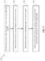
- FIG. 7 is a flow diagram illustrating an example method 700 of fast overvoltage protection via digital control, according to aspects of the subject technology.
- the method 700 receiving, at a receiver (e.g., 104 of FIG. 1 ) of the transceiver (e.g., 100 of FIG. 1 ), one or more link pulses (e.g., 130 and 140 of FIG. 1 ) and signals ( 710 ).
- the method further includes detecting, by the receiver (e.g., 104 of FIG. 1 ), an overvoltage caused by a link pule (e.g., 140 pf FIG. 1 ) ( 720 ).
- the receiver sends an overvoltage signal (e.g., 112 of FIG.
- the control circuit controls an output of a transmitter (e.g., 102 of FIG. 1 ) of the transceiver in response to the overvoltage signal ( 740 ).
- Controlling the output of the transmitter is by disabling the output of the transmitter for a programmable time period (e.g., Tp of FIG. 4 ).
- the link pulse is receivable from the transmitter when a link between the transceiver and a far-end transceiver is not active.
- a processor configured to monitor and control an operation or a component may also mean the processor being programmed to monitor and control the operation or the processor being operable to monitor and control the operation.
- a processor configured to execute code can be construed as a processor programmed to execute code or operable to execute code.
- a phrase such as an “aspect” does not imply that such aspect is essential to the subject technology or that such aspect applies to all configurations of the subject technology.
- a disclosure relating to an aspect may apply to all configurations, or one or more configurations.
- a phrase such as an aspect may refer to one or more aspects and vice versa.
- a phrase such as a “configuration” does not imply that such configuration is essential to the subject technology or that such configuration applies to all configurations of the subject technology.
- a disclosure relating to a configuration may apply to all configurations, or one or more configurations.
- a phrase such as a configuration may refer to one or more configurations and vice versa.
- example is used herein to mean “serving as an example or illustration.” Any aspect or design described herein as “example” is not necessarily to be construed as preferred or advantageous over other aspects or designs.
Landscapes
- Engineering & Computer Science (AREA)
- Computer Networks & Wireless Communication (AREA)
- Signal Processing (AREA)
- Theoretical Computer Science (AREA)
- Physics & Mathematics (AREA)
- Electromagnetism (AREA)
- Power Engineering (AREA)
- Protection Of Static Devices (AREA)
Abstract
Description
Claims (20)
Priority Applications (1)
| Application Number | Priority Date | Filing Date | Title |
|---|---|---|---|
| US15/955,632 US10903641B2 (en) | 2018-04-17 | 2018-04-17 | Fast overvoltage protection circuit with digital control |
Applications Claiming Priority (1)
| Application Number | Priority Date | Filing Date | Title |
|---|---|---|---|
| US15/955,632 US10903641B2 (en) | 2018-04-17 | 2018-04-17 | Fast overvoltage protection circuit with digital control |
Publications (2)
| Publication Number | Publication Date |
|---|---|
| US20190319444A1 US20190319444A1 (en) | 2019-10-17 |
| US10903641B2 true US10903641B2 (en) | 2021-01-26 |
Family
ID=68162268
Family Applications (1)
| Application Number | Title | Priority Date | Filing Date |
|---|---|---|---|
| US15/955,632 Active 2039-04-10 US10903641B2 (en) | 2018-04-17 | 2018-04-17 | Fast overvoltage protection circuit with digital control |
Country Status (1)
| Country | Link |
|---|---|
| US (1) | US10903641B2 (en) |
Citations (5)
| Publication number | Priority date | Publication date | Assignee | Title |
|---|---|---|---|---|
| US20060179372A1 (en) * | 2004-12-20 | 2006-08-10 | Volk Andrew M | Signal drive de-emphasis control for serial bus |
| US20140063666A1 (en) * | 2012-08-29 | 2014-03-06 | Qualcomm Incorporated | Wireless power overvoltage protection circuit with reduced power dissipation |
| US20170294798A1 (en) * | 2016-04-12 | 2017-10-12 | Lg Electronics Inc. | Wireless power transfer method and wireless power transmitter |
| US20190235041A1 (en) * | 2016-06-29 | 2019-08-01 | Lg Innotek Co., Ltd. | Wireless power transmission method and device in wireless charging system |
| US10547212B2 (en) * | 2016-11-08 | 2020-01-28 | Rohm Co., Ltd. | Wireless power receiver, control method thereof, power receiving control circuit, and electronic apparatus |
-
2018
- 2018-04-17 US US15/955,632 patent/US10903641B2/en active Active
Patent Citations (5)
| Publication number | Priority date | Publication date | Assignee | Title |
|---|---|---|---|---|
| US20060179372A1 (en) * | 2004-12-20 | 2006-08-10 | Volk Andrew M | Signal drive de-emphasis control for serial bus |
| US20140063666A1 (en) * | 2012-08-29 | 2014-03-06 | Qualcomm Incorporated | Wireless power overvoltage protection circuit with reduced power dissipation |
| US20170294798A1 (en) * | 2016-04-12 | 2017-10-12 | Lg Electronics Inc. | Wireless power transfer method and wireless power transmitter |
| US20190235041A1 (en) * | 2016-06-29 | 2019-08-01 | Lg Innotek Co., Ltd. | Wireless power transmission method and device in wireless charging system |
| US10547212B2 (en) * | 2016-11-08 | 2020-01-28 | Rohm Co., Ltd. | Wireless power receiver, control method thereof, power receiving control circuit, and electronic apparatus |
Also Published As
| Publication number | Publication date |
|---|---|
| US20190319444A1 (en) | 2019-10-17 |
Similar Documents
| Publication | Publication Date | Title |
|---|---|---|
| US10120406B1 (en) | Adaptive common mode dimmer | |
| WO2016061748A1 (en) | Transimpedance amplifier (tia) having an enlarged dynamic range and optical devices using the same | |
| US20230188097A1 (en) | Differential signal amplification circuit, digital isolator, and digital receiver | |
| CN106961272B (en) | Common-mode transient immunity circuit for optical isolator simulation | |
| US7183793B2 (en) | Systems and methods for reducing electromagnetic emissions from a controller area network transceiver | |
| US20180341615A1 (en) | Differential bus receiver | |
| US5764695A (en) | Adaptive line equalizer | |
| US20160080183A1 (en) | Demodulation of on-off-key modulated signals in signal isolator systems | |
| US9973356B1 (en) | Slicer and decision feedback equalization circuitry | |
| US20140192841A1 (en) | Ultra-wideband loss of signal detector at a receiver in a high speed serializer/deserializer (serdes) application | |
| US11398934B1 (en) | Ultra-high-speed PAM-N CMOS inverter serial link | |
| US10903641B2 (en) | Fast overvoltage protection circuit with digital control | |
| KR100569749B1 (en) | Circuit for data dependent voltage bias level | |
| US10797704B2 (en) | Differential signal transfer systems and associated methods | |
| US8983402B2 (en) | Transceiver with wake up detection | |
| Lee et al. | 0.37-pJ/b/dB PAM-4 transmitter and adaptive receiver with fixed data and threshold levels for 12-m automotive camera link | |
| WO2022246645A1 (en) | Sending circuit of controller area network (can) transceiver and can transceiver | |
| KR20180038286A (en) | Transmitter and system including the same | |
| US10250338B1 (en) | Transmitter drive with improved transmitter performance and reliability | |
| US11671142B2 (en) | Electromagnetic interference cancellation for wireline receivers, with safety function | |
| US11424776B2 (en) | Electromagnetic interference cancellation for wireline receivers | |
| US10700886B2 (en) | Driver apparatus for a differential bus and corresponding method | |
| US10622956B2 (en) | Signal level detection and overrange signal limiter and clamp for electronic circuits | |
| US10666466B2 (en) | Semiconductor integrated circuit, receiving device, and communication system | |
| US11115151B1 (en) | Method and apparatus for fast retraining of ethernet transceivers based on trickling error |
Legal Events
| Date | Code | Title | Description |
|---|---|---|---|
| FEPP | Fee payment procedure |
Free format text: ENTITY STATUS SET TO UNDISCOUNTED (ORIGINAL EVENT CODE: BIG.); ENTITY STATUS OF PATENT OWNER: LARGE ENTITY |
|
| AS | Assignment |
Owner name: AVAGO TECHNOLOGIES GENERAL IP (SINGAPORE) PTE. LTD Free format text: ASSIGNMENT OF ASSIGNORS INTEREST;ASSIGNORS:WESTRA, JAN ROELOF;MULDER, JAN;REEL/FRAME:045593/0364 Effective date: 20180417 Owner name: AVAGO TECHNOLOGIES GENERAL IP (SINGAPORE) PTE. LTD., SINGAPORE Free format text: ASSIGNMENT OF ASSIGNORS INTEREST;ASSIGNORS:WESTRA, JAN ROELOF;MULDER, JAN;REEL/FRAME:045593/0364 Effective date: 20180417 |
|
| AS | Assignment |
Owner name: AVAGO TECHNOLOGIES INTERNATIONAL SALES PTE. LIMITE Free format text: MERGER;ASSIGNOR:AVAGO TECHNOLOGIES GENERAL IP (SINGAPORE) PTE. LTD.;REEL/FRAME:047231/0369 Effective date: 20180509 Owner name: AVAGO TECHNOLOGIES INTERNATIONAL SALES PTE. LIMITED, SINGAPORE Free format text: MERGER;ASSIGNOR:AVAGO TECHNOLOGIES GENERAL IP (SINGAPORE) PTE. LTD.;REEL/FRAME:047231/0369 Effective date: 20180509 |
|
| AS | Assignment |
Owner name: AVAGO TECHNOLOGIES INTERNATIONAL SALES PTE. LIMITE Free format text: CORRECTIVE ASSIGNMENT TO CORRECT THE EXECUTION DATE OF THE MERGER AND APPLICATION NOS. 13/237,550 AND 16/103,107 FROM THE MERGER PREVIOUSLY RECORDED ON REEL 047231 FRAME 0369. ASSIGNOR(S) HEREBY CONFIRMS THE MERGER;ASSIGNOR:AVAGO TECHNOLOGIES GENERAL IP (SINGAPORE) PTE. LTD.;REEL/FRAME:048549/0113 Effective date: 20180905 Owner name: AVAGO TECHNOLOGIES INTERNATIONAL SALES PTE. LIMITED, SINGAPORE Free format text: CORRECTIVE ASSIGNMENT TO CORRECT THE EXECUTION DATE OF THE MERGER AND APPLICATION NOS. 13/237,550 AND 16/103,107 FROM THE MERGER PREVIOUSLY RECORDED ON REEL 047231 FRAME 0369. ASSIGNOR(S) HEREBY CONFIRMS THE MERGER;ASSIGNOR:AVAGO TECHNOLOGIES GENERAL IP (SINGAPORE) PTE. LTD.;REEL/FRAME:048549/0113 Effective date: 20180905 |
|
| STPP | Information on status: patent application and granting procedure in general |
Free format text: NON FINAL ACTION MAILED |
|
| STPP | Information on status: patent application and granting procedure in general |
Free format text: RESPONSE TO NON-FINAL OFFICE ACTION ENTERED AND FORWARDED TO EXAMINER |
|
| STPP | Information on status: patent application and granting procedure in general |
Free format text: PUBLICATIONS -- ISSUE FEE PAYMENT VERIFIED |
|
| STCF | Information on status: patent grant |
Free format text: PATENTED CASE |
|
| CC | Certificate of correction |