US10890848B2 - Material for detecting photoresist and method of fabricating semiconductor device using the same - Google Patents
Material for detecting photoresist and method of fabricating semiconductor device using the same Download PDFInfo
- Publication number
- US10890848B2 US10890848B2 US16/037,232 US201816037232A US10890848B2 US 10890848 B2 US10890848 B2 US 10890848B2 US 201816037232 A US201816037232 A US 201816037232A US 10890848 B2 US10890848 B2 US 10890848B2
- Authority
- US
- United States
- Prior art keywords
- photoresist
- semiconductor device
- fabricating
- detecting
- molecule
- Prior art date
- Legal status (The legal status is an assumption and is not a legal conclusion. Google has not performed a legal analysis and makes no representation as to the accuracy of the status listed.)
- Active, expires
Links
- FWEOQOXTVHGIFQ-UHFFFAOYSA-N [H]N(c1ccccc1)c1cccc2cccc(S(=O)(=O)O)c12 Chemical compound [H]N(c1ccccc1)c1cccc2cccc(S(=O)(=O)O)c12 FWEOQOXTVHGIFQ-UHFFFAOYSA-N 0.000 description 2
- ORILYTVJVMAKLC-UHFFFAOYSA-N C1C2CC3CC1CC(C2)C3 Chemical compound C1C2CC3CC1CC(C2)C3 ORILYTVJVMAKLC-UHFFFAOYSA-N 0.000 description 1
- OWIYFQFUDBJARS-UHFFFAOYSA-N C1C2CC3CC1CC(C2)C3.CCN(CC)C1=CC=C2C=C(C(C)=O)C(=O)OC2=C1.O=C(O)C12CC3CC(CC(C3)C1)C2.Oc1ccccc1.[H]N(c1ccccc1)c1cccc2cccc(S(=O)(=O)O)c12 Chemical compound C1C2CC3CC1CC(C2)C3.CCN(CC)C1=CC=C2C=C(C(C)=O)C(=O)OC2=C1.O=C(O)C12CC3CC(CC(C3)C1)C2.Oc1ccccc1.[H]N(c1ccccc1)c1cccc2cccc(S(=O)(=O)O)c12 OWIYFQFUDBJARS-UHFFFAOYSA-N 0.000 description 1
- WHCPTFFIERCDSB-UHFFFAOYSA-N CCN(CC)C1=CC=C2C=C(C(=O)O)C(=O)OC2=C1 Chemical compound CCN(CC)C1=CC=C2C=C(C(=O)O)C(=O)OC2=C1 WHCPTFFIERCDSB-UHFFFAOYSA-N 0.000 description 1
- JIMXXGFJRDUSRO-UHFFFAOYSA-N O=C(O)C12CC3CC(CC(C3)C1)C2 Chemical compound O=C(O)C12CC3CC(CC(C3)C1)C2 JIMXXGFJRDUSRO-UHFFFAOYSA-N 0.000 description 1
- ISWSIDIOOBJBQZ-UHFFFAOYSA-N Oc1ccccc1 Chemical compound Oc1ccccc1 ISWSIDIOOBJBQZ-UHFFFAOYSA-N 0.000 description 1
Images


Classifications
-
- G—PHYSICS
- G03—PHOTOGRAPHY; CINEMATOGRAPHY; ANALOGOUS TECHNIQUES USING WAVES OTHER THAN OPTICAL WAVES; ELECTROGRAPHY; HOLOGRAPHY
- G03F—PHOTOMECHANICAL PRODUCTION OF TEXTURED OR PATTERNED SURFACES, e.g. FOR PRINTING, FOR PROCESSING OF SEMICONDUCTOR DEVICES; MATERIALS THEREFOR; ORIGINALS THEREFOR; APPARATUS SPECIALLY ADAPTED THEREFOR
- G03F7/00—Photomechanical, e.g. photolithographic, production of textured or patterned surfaces, e.g. printing surfaces; Materials therefor, e.g. comprising photoresists; Apparatus specially adapted therefor
- G03F7/26—Processing photosensitive materials; Apparatus therefor
- G03F7/40—Treatment after imagewise removal, e.g. baking
-
- G—PHYSICS
- G01—MEASURING; TESTING
- G01N—INVESTIGATING OR ANALYSING MATERIALS BY DETERMINING THEIR CHEMICAL OR PHYSICAL PROPERTIES
- G01N21/00—Investigating or analysing materials by the use of optical means, i.e. using sub-millimetre waves, infrared, visible or ultraviolet light
- G01N21/62—Systems in which the material investigated is excited whereby it emits light or causes a change in wavelength of the incident light
- G01N21/63—Systems in which the material investigated is excited whereby it emits light or causes a change in wavelength of the incident light optically excited
- G01N21/64—Fluorescence; Phosphorescence
- G01N21/6428—Measuring fluorescence of fluorescent products of reactions or of fluorochrome labelled reactive substances, e.g. measuring quenching effects, using measuring "optrodes"
- G01N21/643—Measuring fluorescence of fluorescent products of reactions or of fluorochrome labelled reactive substances, e.g. measuring quenching effects, using measuring "optrodes" non-biological material
-
- C—CHEMISTRY; METALLURGY
- C08—ORGANIC MACROMOLECULAR COMPOUNDS; THEIR PREPARATION OR CHEMICAL WORKING-UP; COMPOSITIONS BASED THEREON
- C08B—POLYSACCHARIDES; DERIVATIVES THEREOF
- C08B37/00—Preparation of polysaccharides not provided for in groups C08B1/00 - C08B35/00; Derivatives thereof
- C08B37/0006—Homoglycans, i.e. polysaccharides having a main chain consisting of one single sugar, e.g. colominic acid
- C08B37/0009—Homoglycans, i.e. polysaccharides having a main chain consisting of one single sugar, e.g. colominic acid alpha-D-Glucans, e.g. polydextrose, alternan, glycogen; (alpha-1,4)(alpha-1,6)-D-Glucans; (alpha-1,3)(alpha-1,4)-D-Glucans, e.g. isolichenan or nigeran; (alpha-1,4)-D-Glucans; (alpha-1,3)-D-Glucans, e.g. pseudonigeran; Derivatives thereof
- C08B37/0012—Cyclodextrin [CD], e.g. cycle with 6 units (alpha), with 7 units (beta) and with 8 units (gamma), large-ring cyclodextrin or cycloamylose with 9 units or more; Derivatives thereof
- C08B37/0015—Inclusion compounds, i.e. host-guest compounds, e.g. polyrotaxanes
-
- C—CHEMISTRY; METALLURGY
- C08—ORGANIC MACROMOLECULAR COMPOUNDS; THEIR PREPARATION OR CHEMICAL WORKING-UP; COMPOSITIONS BASED THEREON
- C08L—COMPOSITIONS OF MACROMOLECULAR COMPOUNDS
- C08L5/00—Compositions of polysaccharides or of their derivatives not provided for in groups C08L1/00 or C08L3/00
- C08L5/16—Cyclodextrin; Derivatives thereof
-
- C—CHEMISTRY; METALLURGY
- C09—DYES; PAINTS; POLISHES; NATURAL RESINS; ADHESIVES; COMPOSITIONS NOT OTHERWISE PROVIDED FOR; APPLICATIONS OF MATERIALS NOT OTHERWISE PROVIDED FOR
- C09K—MATERIALS FOR MISCELLANEOUS APPLICATIONS, NOT PROVIDED FOR ELSEWHERE
- C09K11/00—Luminescent materials, e.g. electroluminescent or chemiluminescent
- C09K11/06—Luminescent materials, e.g. electroluminescent or chemiluminescent containing organic luminescent materials
-
- G—PHYSICS
- G01—MEASURING; TESTING
- G01N—INVESTIGATING OR ANALYSING MATERIALS BY DETERMINING THEIR CHEMICAL OR PHYSICAL PROPERTIES
- G01N21/00—Investigating or analysing materials by the use of optical means, i.e. using sub-millimetre waves, infrared, visible or ultraviolet light
- G01N21/84—Systems specially adapted for particular applications
- G01N21/88—Investigating the presence of flaws or contamination
- G01N21/91—Investigating the presence of flaws or contamination using penetration of dyes, e.g. fluorescent ink
-
- G—PHYSICS
- G01—MEASURING; TESTING
- G01N—INVESTIGATING OR ANALYSING MATERIALS BY DETERMINING THEIR CHEMICAL OR PHYSICAL PROPERTIES
- G01N21/00—Investigating or analysing materials by the use of optical means, i.e. using sub-millimetre waves, infrared, visible or ultraviolet light
- G01N21/84—Systems specially adapted for particular applications
- G01N21/88—Investigating the presence of flaws or contamination
- G01N21/94—Investigating contamination, e.g. dust
-
- G—PHYSICS
- G01—MEASURING; TESTING
- G01N—INVESTIGATING OR ANALYSING MATERIALS BY DETERMINING THEIR CHEMICAL OR PHYSICAL PROPERTIES
- G01N21/00—Investigating or analysing materials by the use of optical means, i.e. using sub-millimetre waves, infrared, visible or ultraviolet light
- G01N21/84—Systems specially adapted for particular applications
- G01N21/88—Investigating the presence of flaws or contamination
- G01N21/95—Investigating the presence of flaws or contamination characterised by the material or shape of the object to be examined
- G01N21/9501—Semiconductor wafers
-
- G—PHYSICS
- G03—PHOTOGRAPHY; CINEMATOGRAPHY; ANALOGOUS TECHNIQUES USING WAVES OTHER THAN OPTICAL WAVES; ELECTROGRAPHY; HOLOGRAPHY
- G03F—PHOTOMECHANICAL PRODUCTION OF TEXTURED OR PATTERNED SURFACES, e.g. FOR PRINTING, FOR PROCESSING OF SEMICONDUCTOR DEVICES; MATERIALS THEREFOR; ORIGINALS THEREFOR; APPARATUS SPECIALLY ADAPTED THEREFOR
- G03F7/00—Photomechanical, e.g. photolithographic, production of textured or patterned surfaces, e.g. printing surfaces; Materials therefor, e.g. comprising photoresists; Apparatus specially adapted therefor
- G03F7/0002—Lithographic processes using patterning methods other than those involving the exposure to radiation, e.g. by stamping
-
- G—PHYSICS
- G03—PHOTOGRAPHY; CINEMATOGRAPHY; ANALOGOUS TECHNIQUES USING WAVES OTHER THAN OPTICAL WAVES; ELECTROGRAPHY; HOLOGRAPHY
- G03F—PHOTOMECHANICAL PRODUCTION OF TEXTURED OR PATTERNED SURFACES, e.g. FOR PRINTING, FOR PROCESSING OF SEMICONDUCTOR DEVICES; MATERIALS THEREFOR; ORIGINALS THEREFOR; APPARATUS SPECIALLY ADAPTED THEREFOR
- G03F7/00—Photomechanical, e.g. photolithographic, production of textured or patterned surfaces, e.g. printing surfaces; Materials therefor, e.g. comprising photoresists; Apparatus specially adapted therefor
- G03F7/16—Coating processes; Apparatus therefor
-
- G—PHYSICS
- G03—PHOTOGRAPHY; CINEMATOGRAPHY; ANALOGOUS TECHNIQUES USING WAVES OTHER THAN OPTICAL WAVES; ELECTROGRAPHY; HOLOGRAPHY
- G03F—PHOTOMECHANICAL PRODUCTION OF TEXTURED OR PATTERNED SURFACES, e.g. FOR PRINTING, FOR PROCESSING OF SEMICONDUCTOR DEVICES; MATERIALS THEREFOR; ORIGINALS THEREFOR; APPARATUS SPECIALLY ADAPTED THEREFOR
- G03F7/00—Photomechanical, e.g. photolithographic, production of textured or patterned surfaces, e.g. printing surfaces; Materials therefor, e.g. comprising photoresists; Apparatus specially adapted therefor
- G03F7/26—Processing photosensitive materials; Apparatus therefor
- G03F7/30—Imagewise removal using liquid means
- G03F7/32—Liquid compositions therefor, e.g. developers
- G03F7/325—Non-aqueous compositions
- G03F7/327—Non-aqueous alkaline compositions, e.g. anhydrous quaternary ammonium salts
-
- H—ELECTRICITY
- H10—SEMICONDUCTOR DEVICES; ELECTRIC SOLID-STATE DEVICES NOT OTHERWISE PROVIDED FOR
- H10P—GENERIC PROCESSES OR APPARATUS FOR THE MANUFACTURE OR TREATMENT OF DEVICES COVERED BY CLASS H10
- H10P76/00—Manufacture or treatment of masks on semiconductor bodies, e.g. by lithography or photolithography
- H10P76/20—Manufacture or treatment of masks on semiconductor bodies, e.g. by lithography or photolithography of masks comprising organic materials
- H10P76/204—Manufacture or treatment of masks on semiconductor bodies, e.g. by lithography or photolithography of masks comprising organic materials of organic photoresist masks
-
- C—CHEMISTRY; METALLURGY
- C09—DYES; PAINTS; POLISHES; NATURAL RESINS; ADHESIVES; COMPOSITIONS NOT OTHERWISE PROVIDED FOR; APPLICATIONS OF MATERIALS NOT OTHERWISE PROVIDED FOR
- C09K—MATERIALS FOR MISCELLANEOUS APPLICATIONS, NOT PROVIDED FOR ELSEWHERE
- C09K2211/00—Chemical nature of organic luminescent or tenebrescent compounds
- C09K2211/10—Non-macromolecular compounds
- C09K2211/1018—Heterocyclic compounds
- C09K2211/1025—Heterocyclic compounds characterised by ligands
- C09K2211/1029—Heterocyclic compounds characterised by ligands containing one nitrogen atom as the heteroatom
-
- C—CHEMISTRY; METALLURGY
- C09—DYES; PAINTS; POLISHES; NATURAL RESINS; ADHESIVES; COMPOSITIONS NOT OTHERWISE PROVIDED FOR; APPLICATIONS OF MATERIALS NOT OTHERWISE PROVIDED FOR
- C09K—MATERIALS FOR MISCELLANEOUS APPLICATIONS, NOT PROVIDED FOR ELSEWHERE
- C09K2211/00—Chemical nature of organic luminescent or tenebrescent compounds
- C09K2211/10—Non-macromolecular compounds
- C09K2211/1018—Heterocyclic compounds
- C09K2211/1025—Heterocyclic compounds characterised by ligands
- C09K2211/1088—Heterocyclic compounds characterised by ligands containing oxygen as the only heteroatom
-
- G—PHYSICS
- G01—MEASURING; TESTING
- G01N—INVESTIGATING OR ANALYSING MATERIALS BY DETERMINING THEIR CHEMICAL OR PHYSICAL PROPERTIES
- G01N21/00—Investigating or analysing materials by the use of optical means, i.e. using sub-millimetre waves, infrared, visible or ultraviolet light
- G01N21/62—Systems in which the material investigated is excited whereby it emits light or causes a change in wavelength of the incident light
- G01N21/63—Systems in which the material investigated is excited whereby it emits light or causes a change in wavelength of the incident light optically excited
- G01N21/64—Fluorescence; Phosphorescence
- G01N21/6428—Measuring fluorescence of fluorescent products of reactions or of fluorochrome labelled reactive substances, e.g. measuring quenching effects, using measuring "optrodes"
- G01N2021/6439—Measuring fluorescence of fluorescent products of reactions or of fluorochrome labelled reactive substances, e.g. measuring quenching effects, using measuring "optrodes" with indicators, stains, dyes, tags, labels, marks
-
- G—PHYSICS
- G01—MEASURING; TESTING
- G01N—INVESTIGATING OR ANALYSING MATERIALS BY DETERMINING THEIR CHEMICAL OR PHYSICAL PROPERTIES
- G01N21/00—Investigating or analysing materials by the use of optical means, i.e. using sub-millimetre waves, infrared, visible or ultraviolet light
- G01N21/84—Systems specially adapted for particular applications
- G01N2021/8461—Investigating impurities in semiconductor, e.g. Silicon
Definitions
- a material for detecting photoresist and a method of fabricating a semiconductor device using the same.
- the wavelength of an exposure light source decreases, and a process is converted into a process using I-line (365 nm), KrF laser (248 nm), or ArF laser (193 nm), and in line with the conversion, the development of various materials is being conducted.
- I-line 365 nm
- KrF laser 248 nm
- ArF laser (193 nm)
- the size of a semiconductor device decreases, and patterns which are distorted due to residues or contaminants produced during processes affect the performance, yield and reliability of the semiconductor device, requirements on verifying materials in advance are increasing.
- Photoresist is a photosensitive polymer compound, and a photoresist pattern may be formed on a wafer by physical change due to the chemical change of components on exposure and by selective dissolution of an exposed part and an unexposed part during a developing process.
- inspection after exposure if a photoresist pattern is formed into a desired shape or if photoresist residue are left after removing the photoresist pattern, may be required.
- a material for detecting photoresist is provided.
- a material for detecting photoresist includes a macrocyclic molecule having a hollow structure and a fluorescent substance which is labeled on the macrocyclic molecule, wherein the macrocyclic molecule is at least one of cyclodexrin, cucurbituril, calixarene, pillararene and catenane.
- a material for detecting photoresist includes a macrocyclic molecule having a hollow structure and a fluorescent substance which is labeled on the macrocyclic molecule, wherein a target molecule on a surface of the photoresist is inserted into the hollow structure, and thus the material for detecting photoresist bonds to the photoresist.
- a method of fabricating a semiconductor device includes a forming step of forming a photoresist layer including a first part and a second part on a wafer, a removing step of removing the first part and leaving the second part of the photoresist layer, a bonding step of bonding a material for detecting photoresist to a surface of the second part, and an inspecting step of inspecting the second part.
- FIG. 1 shows a structure of a material for detecting photoresist according to example embodiments
- FIG. 2 is a flowchart showing a manufacturing method of a semiconductor device, by which photoresist is detected according to example embodiments;
- FIGS. 3A to 3D are cross-sectional views showing a manufacturing method of a semiconductor device, by which photoresist is detected according to example embodiments;
- FIG. 4 is an enlarged diagram on the “P 1 ” part of FIG. 3C ;
- FIG. 5 shows example cyclodextrin (CD) structures
- FIG. 6 shows example cucurbituril (CB) structures
- FIG. 7 shows example calixarene structures
- FIG. 8 shows example pillararene structures
- FIG. 9 shows example catenane structures.
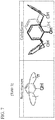
- FIG. 1 shows a structure of a material for detecting photoresist according to example embodiments.
- a material 5 for detecting photoresist may include a macrocyclic molecule 5 a having a hollow structure and a fluorescent substance 5 b labeled on the macrocyclic molecule 5 a .
- the inner part of the hollow structure of the macrocyclic molecule 5 a may be hydrophobic.
- the macrocyclic molecule 5 a may be, for example, at least one of cyclodextrin (CD), cucurbituril (CB), calixarene, pillararene and catenane.
- CD cyclodextrin
- CB cucurbituril
- calixarene calixarene
- pillararene pillararene
- catenane catenane
- the cyclodextrin (CD) may have a structure in FIG. 5 (Table 1 therein).
- the cyclodextrin including 6 glucose molecules may be named ⁇ -CD
- the cyclodextrin including 7 glucose molecules may be named ⁇ -CD
- the cyclodextrin including 8 glucose molecules may be named ⁇ -CD.
- the cucurbituril (CB) may have a structure in FIG. 6 (Table 2 therein).
- the cucurbituril (CB) may have a hollow three-dimensional structure.
- the calixarene may have a structure in FIG. 7 (Table 3 therein).
- the calixarene may have a hollow three-dimensional structure.
- the pillararene may have a structure in FIG. 8 (Table 4 therein).
- the pillararene may have a hollow three-dimensional structure.
- the catenane may have a molecular structure in which two or more macrocyclic molecules are mechanically combined.
- the catenane may have, for example, a structure in FIG. 9 (Table 5 therein).
- all macrocyclic molecules shown in FIG. 5 to FIG. 9 may have a hollow structure.
- Some of terminals of the cyclodextrin (CD), the cucurbituril (CB), the calixarene, the pillararene, and the catenane may be substituted with other functional group or molecule.
- the fluorescent substance 5 b may be, for example, a cyanine (Cy)-based or rhodamine-based fluorescent substance.
- the cyanine-based fluorescent substance may be, for example, Cy2, Cy3, Cy3B, Cy3.5, Cy5, Cy5.5, or Cy7.
- the rhodamine-based fluorescent substance may be, for example, Rhodamine B, Rhodamine 6G, or Rhodamine 123.
- Particular examples of the material 5 for detecting photoresist may be cyanine-labeled beta-cyclodextrin (cyanine-labeled ⁇ -CD) or rhodamine-labeled beta-cyclodextrin (rhodamine-labeled ⁇ -CD).
- FIG. 2 is a flowchart showing a manufacturing method of a semiconductor device, by which photoresist is detected according to example embodiments.
- FIGS. 3A to 3D are cross-sectional views showing a manufacturing method of a semiconductor device, by which photoresist is detected according to example embodiments.
- FIG. 4 is an enlarged diagram on the “P 1 ” part of FIG. 3C .
- a photoresist layer 3 including a first part 3 a and a second part 3 b is formed on a wafer 1 (S 10 ).
- an insulating layer or a conductive layer to be etched may be formed on the wafer 1 prior to forming the photoresist layer 3 .
- the photoresist layer 3 may be formed, for example, by coating and baking processes.
- the photoresist layer 3 may be a polyhydroxystyrene type or a polyacrylate type.
- the photoresist layer 3 may include a target molecule G which is bonded to a portion of the polyacrylate.
- the target molecule G may be, for example, at least one of adamantane, a cyclic carbon compound, a cycloalkyl group, a saturated hydrocarbon and an aromatic hydrocarbon.
- the target molecule G may have a structure shown in Table 6.
- Target molecule 1 Target molecule 2
- Target molecule 3 Target molecule 4
- Target molecule 5 Target molecule 5
- the first part 3 a of the photoresist layer 3 may be removed and the second part 3 b thereof may be left (S 20 ).
- the second part 3 b may be a photoresist pattern or photoresist residue.
- the second part 3 b may be formed by an exposure process and a developing process. In this case, the subsequent inspection of the second part 3 b may be conducted for inspecting whether a photoresist pattern is formed in a desired shape after the exposure and developing processes.
- the first part 3 a or the second part 3 b may be an exposed part by the exposure process.
- the first part 3 a may be removed by the developing process.
- the photoresist layer 3 may be hydrophobic before performing the exposure process.
- the exposed part may be changed into a hydrophilic part. If the first part 3 a is an exposed part, this part may be changed into a hydrophilic part.
- TMAH tetramethylammonium hydroxide
- N-butyl acetate NAA
- the first part 3 a may be removed by a strip process (or a cleaning step).
- the strip process may be performed using tetramethylammonium hydroxide (TMAH).
- TMAH tetramethylammonium hydroxide
- the subsequent inspection of the second part 3 b may be performed for checking the performance of the photoresist.
- the material 5 for detecting photoresist may be bonded to the surface of the second part 3 b (S 30 ).
- the material 5 for detecting photoresist may be identical or similar to that explained referring to FIG. 1 .
- the target molecule G may be inserted into the hollow structure of the macrocyclic molecule 5 a .
- the step of bonding the material 5 for detecting photoresist to the surface of the second part 3 b may include supplying the material 5 for detecting photoresist by a coating, dipping or spraying method.
- the step of bonding the material 5 for detecting photoresist with the surface of the second part 3 b may further include a step of performing a cleaning step after supplying the material 5 for detecting photoresist to remove the material 5 for detecting photoresist which is not bonded to the second part 3 b .
- the cleaning step may be performed using water.
- a solution including the material 5 for detecting photoresist may be prepared. After bonding the material 5 for detecting photoresist to the surface of the second part 3 b by coating or spraying the solution on the wafer 1 in the state of FIG. 3B , or dipping the wafer 1 into the solution, a cleaning process may be performed.
- the binding affinity (K a ) between the target molecule G and the macrocyclic molecule 5 a of the material 5 for detecting photoresist may be about 10 4 -10 5 M ⁇ 1 .
- the binding affinity (K a ) may be about 10 5 M ⁇ 1 , and a stable composite is found to be formed.
- beta-cyclodextrin is used as the macrocyclic molecule 5 a and target molecules 1-4 of Table 6 are used as the target molecule G, the binding affinity may be shown as in Table 7.
- the second part 3 b is inspected (S 40 ).
- the inspection of the second part 3 b is performed by measuring fluorescence.
- the measurement of fluorescence may be conducted by using, for example, an inspection apparatus 10 such as a confocal microscopy.
- the residues of photoresist after cleaning process may be inspected. Even though the photoresist residue are minute and several nanometer sizes, detection may be possible. Accordingly, photoresist with excellent performance may be prepared.
- the photoresist pattern may be inspected after exposure and developing processes if a desired shape is formed well. If the photoresist pattern is formed into a desired shape, underlying insulating layer or conductive layer may be etched using the photoresist pattern as an etching mask. Thus, a semiconductor device having improved reliability may be manufactured.
- the material for detecting photoresist includes a macrocyclic molecule which is marked with a fluorescent substance, and into the hollow structure of the macrocyclic molecule, a target molecule on the surface of the photoresist may be inserted.
- the material for detecting photoresist may be bonded to the photoresist, and the photoresist may be detected by measuring fluorescence. Accordingly, the leaving of the residues of the photoresist after a cleaning process may be inspected. Accordingly, photoresist with excellent performance may be prepared.
- the shape of a photoresist pattern may be inspected after exposure and developing processes if well formed, and thus, a semiconductor device having improved reliability may be manufactured.
Landscapes
- Chemical & Material Sciences (AREA)
- Health & Medical Sciences (AREA)
- Physics & Mathematics (AREA)
- Life Sciences & Earth Sciences (AREA)
- General Physics & Mathematics (AREA)
- Immunology (AREA)
- Biochemistry (AREA)
- General Health & Medical Sciences (AREA)
- Chemical Kinetics & Catalysis (AREA)
- Pathology (AREA)
- Analytical Chemistry (AREA)
- Organic Chemistry (AREA)
- Molecular Biology (AREA)
- Polymers & Plastics (AREA)
- Medicinal Chemistry (AREA)
- Engineering & Computer Science (AREA)
- Materials Engineering (AREA)
- Optics & Photonics (AREA)
- Nuclear Medicine, Radiotherapy & Molecular Imaging (AREA)
- Investigating, Analyzing Materials By Fluorescence Or Luminescence (AREA)
- Exposure Of Semiconductors, Excluding Electron Or Ion Beam Exposure (AREA)
- Photosensitive Polymer And Photoresist Processing (AREA)
Abstract
Description
| TABLE 6 | |
 |
|
 |
|
 |
|
 |
|
|
|
|
| TABLE 7 | |||||
| Target | Target | | Target | ||
| molecule | |||||
| 1 | |
|
|
||
| Log Ka | 4.49 | 5.64 | 6.43 | 5.61 |
| (at PH 7) | ||||
Claims (13)

Applications Claiming Priority (2)
| Application Number | Priority Date | Filing Date | Title |
|---|---|---|---|
| KR10-2017-0176301 | 2017-12-20 | ||
| KR1020170176301A KR102445340B1 (en) | 2017-12-20 | 2017-12-20 | Photoresist detection material and method of manufacturing semiconductor device using same |
Publications (2)
| Publication Number | Publication Date |
|---|---|
| US20190187052A1 US20190187052A1 (en) | 2019-06-20 |
| US10890848B2 true US10890848B2 (en) | 2021-01-12 |
Family
ID=66813860
Family Applications (1)
| Application Number | Title | Priority Date | Filing Date |
|---|---|---|---|
| US16/037,232 Active 2039-02-17 US10890848B2 (en) | 2017-12-20 | 2018-07-17 | Material for detecting photoresist and method of fabricating semiconductor device using the same |
Country Status (3)
| Country | Link |
|---|---|
| US (1) | US10890848B2 (en) |
| KR (1) | KR102445340B1 (en) |
| CN (1) | CN109946928A (en) |
Families Citing this family (6)
| Publication number | Priority date | Publication date | Assignee | Title |
|---|---|---|---|---|
| CN113376968B (en) * | 2020-03-10 | 2023-04-07 | 长鑫存储技术有限公司 | Method for detecting defects of semiconductor manufacturing process |
| CN111320899B (en) * | 2020-03-13 | 2021-09-03 | 四川大学 | Kit and application thereof in preparation of visual organic solvent indicator and writing of confidential documents |
| CN112915985A (en) * | 2021-02-03 | 2021-06-08 | 江苏新视界先进功能纤维创新中心有限公司 | Easy-to-remove regenerated open-chain cucurbituril-based material for treating phenolic wastewater and preparation method thereof |
| CN114907501A (en) * | 2022-06-06 | 2022-08-16 | 北京航空航天大学 | Macrocyclic molecule promoted photoinitiation system, photopolymer material and preparation method |
| CN115872922B (en) * | 2022-12-06 | 2024-06-04 | 盐城工学院 | Main body material based on column [5] arene derivative, and preparation method and application thereof |
| CN116621768B (en) * | 2023-04-21 | 2025-08-26 | 盐城工学院 | A thermally activated delayed fluorescent material based on pillar[5]arene derivatives, its preparation method and OLED application |
Citations (10)
| Publication number | Priority date | Publication date | Assignee | Title |
|---|---|---|---|---|
| WO1991002040A1 (en) | 1989-08-04 | 1991-02-21 | Kosak Kenneth M | Cyclodextrin labels for nucleic acid and biochemical analysis |
| WO1991005605A1 (en) | 1989-10-10 | 1991-05-02 | Kosak Kenneth M | Cyclodextrin labels for immunoassay and biochemical analysis |
| US6091488A (en) * | 1999-03-22 | 2000-07-18 | Beltronics, Inc. | Method of and apparatus for automatic high-speed optical inspection of semi-conductor structures and the like through fluorescent photoresist inspection |
| US20090220381A1 (en) * | 2005-11-15 | 2009-09-03 | Nestec S.A. | Imagewise patterning of films and devices comprising the same |
| KR101022776B1 (en) | 2008-10-22 | 2011-03-16 | 한국원자력연구원 | Calix [4] arene derivatives having cadmium or zinc ion selectivity, methods for preparing the same, methods for detecting cadmium or zinc ions using the same, and fluorescent chemical sensors |
| JP2012082178A (en) | 2010-10-14 | 2012-04-26 | National Institute Of Advanced Industrial Science & Technology | Method for detecting rare earth metal by using calixarene derivative |
| JP2012118319A (en) | 2010-12-01 | 2012-06-21 | Toppan Printing Co Ltd | Method and apparatus for regenerating glass substrate for color filter |
| KR101234026B1 (en) | 2011-01-26 | 2013-02-19 | 금오공과대학교 산학협력단 | Method of distinguishing position isomer of aromatic compounds by using cucurbituril |
| US20150044705A1 (en) | 2013-08-09 | 2015-02-12 | Bio-Rad Laboratories, Inc. | Protein detection using modified cyclodextrins |
| JP2017020992A (en) | 2015-07-15 | 2017-01-26 | Jsr株式会社 | Analysis method |
Family Cites Families (7)
| Publication number | Priority date | Publication date | Assignee | Title |
|---|---|---|---|---|
| US20070042390A1 (en) * | 2005-08-19 | 2007-02-22 | Applied Materials, Inc. A Delaware Corporation | Method and device for critical dimension detection by molecular binding |
| KR100848308B1 (en) * | 2005-11-12 | 2008-07-24 | 학교법인 포항공과대학교 | The application using non-covalent bond between a cucurbituril derivative and a ligand |
| JP5703129B2 (en) * | 2011-05-26 | 2015-04-15 | 住友ベークライト株式会社 | Solid-phase support and method for producing solid-phase support |
| US9316612B2 (en) * | 2013-01-04 | 2016-04-19 | Yale University | Regenerative nanosensor devices |
| CN104740645A (en) * | 2015-03-27 | 2015-07-01 | 南开大学 | Cucurbituril/cyclodextrin/adamantane anthracene ternary supramolecular assembly and preparation method |
| US20180216060A1 (en) * | 2015-07-17 | 2018-08-02 | Academisch Ziekenhuis Leiden (Also Acting Under Th E Name Of Leiden University Medical Center) | Methods and means for the modification of cell surfaces |
| KR20170042432A (en) * | 2015-10-08 | 2017-04-19 | 삼성전자주식회사 | Method for inspecting photoresist pattern |
-
2017
- 2017-12-20 KR KR1020170176301A patent/KR102445340B1/en active Active
-
2018
- 2018-07-17 US US16/037,232 patent/US10890848B2/en active Active
- 2018-12-11 CN CN201811508715.2A patent/CN109946928A/en active Pending
Patent Citations (11)
| Publication number | Priority date | Publication date | Assignee | Title |
|---|---|---|---|---|
| WO1991002040A1 (en) | 1989-08-04 | 1991-02-21 | Kosak Kenneth M | Cyclodextrin labels for nucleic acid and biochemical analysis |
| WO1991005605A1 (en) | 1989-10-10 | 1991-05-02 | Kosak Kenneth M | Cyclodextrin labels for immunoassay and biochemical analysis |
| US6091488A (en) * | 1999-03-22 | 2000-07-18 | Beltronics, Inc. | Method of and apparatus for automatic high-speed optical inspection of semi-conductor structures and the like through fluorescent photoresist inspection |
| US20090220381A1 (en) * | 2005-11-15 | 2009-09-03 | Nestec S.A. | Imagewise patterning of films and devices comprising the same |
| KR101022776B1 (en) | 2008-10-22 | 2011-03-16 | 한국원자력연구원 | Calix [4] arene derivatives having cadmium or zinc ion selectivity, methods for preparing the same, methods for detecting cadmium or zinc ions using the same, and fluorescent chemical sensors |
| JP2012082178A (en) | 2010-10-14 | 2012-04-26 | National Institute Of Advanced Industrial Science & Technology | Method for detecting rare earth metal by using calixarene derivative |
| JP2012118319A (en) | 2010-12-01 | 2012-06-21 | Toppan Printing Co Ltd | Method and apparatus for regenerating glass substrate for color filter |
| KR101234026B1 (en) | 2011-01-26 | 2013-02-19 | 금오공과대학교 산학협력단 | Method of distinguishing position isomer of aromatic compounds by using cucurbituril |
| US20150044705A1 (en) | 2013-08-09 | 2015-02-12 | Bio-Rad Laboratories, Inc. | Protein detection using modified cyclodextrins |
| US9285359B2 (en) | 2013-08-09 | 2016-03-15 | Bio-Rad Laboratories, Inc. | Protein detection using modified cyclodextrins |
| JP2017020992A (en) | 2015-07-15 | 2017-01-26 | Jsr株式会社 | Analysis method |
Also Published As
| Publication number | Publication date |
|---|---|
| KR20190074729A (en) | 2019-06-28 |
| KR102445340B1 (en) | 2022-09-21 |
| CN109946928A (en) | 2019-06-28 |
| US20190187052A1 (en) | 2019-06-20 |
Similar Documents
| Publication | Publication Date | Title |
|---|---|---|
| US10890848B2 (en) | Material for detecting photoresist and method of fabricating semiconductor device using the same | |
| US9810978B2 (en) | Method for lithography patterning | |
| US7494830B2 (en) | Method and device for wafer backside alignment overlay accuracy | |
| US20080280230A1 (en) | Photolithography process including a chemical rinse | |
| US20120295435A1 (en) | Pattern transfer method | |
| DE102019201202B4 (en) | Method of improving heterodyne performance in semiconductor devices | |
| US11280825B2 (en) | Functional prober chip | |
| JP2011133750A (en) | Member with protective film for forming resist pattern, and method for producing the same, and method for producing resist pattern | |
| Teyssedre et al. | A full-process chain assessment for nanoimprint technology on 200-mm industrial platform | |
| Feng et al. | An ultralow background substrate for protein microarray technology | |
| KR20170089271A (en) | Cantilever set for atomic force microscope, apparatus for substrate surface inspection comprising the same, method of analyzing a surface of a semiconductor substrate using the same, and method of forming a micropattern using the same | |
| US20080138746A1 (en) | Pattern formation method using fine pattern formation material for use in semiconductor fabrication step | |
| CN1211817A (en) | Alignment marks of semiconductor substrate and manufacturing method thereof | |
| US9091925B2 (en) | Method for forming silicon-containing resist underlayer film | |
| US7473517B2 (en) | Supercritical developing for a lithographic process | |
| CN101174087A (en) | Process for making photoresist pattern | |
| US20180239237A1 (en) | Photomask and manufacturing method thereof | |
| TW200905508A (en) | Method of determining defects in photomask | |
| KR20090056433A (en) | Manufacturing Method of Semiconductor Device | |
| KR101069434B1 (en) | Photomask manufacturing method using self-assembled molecular layer | |
| CN105719981B (en) | Semiconductor structures and methods of forming them | |
| CN111192233B (en) | Preparation method and preparation device of semiconductor structure | |
| KR20250042665A (en) | Anisotropic conductive film for micro-bump testing and method of manufacturing the same | |
| JP4613695B2 (en) | Manufacturing method of semiconductor device | |
| Shigemori et al. | Defectivity process optimization on immersion topcoat less resist stacks |
Legal Events
| Date | Code | Title | Description |
|---|---|---|---|
| AS | Assignment |
Owner name: SAMSUNG ELECTRONICS CO., LTD., KOREA, REPUBLIC OF Free format text: ASSIGNMENT OF ASSIGNORS INTEREST;ASSIGNORS:JANG, YOONJUNG;KIM, SOOYOUNG;KIM, BOODEUK;AND OTHERS;REEL/FRAME:046371/0806 Effective date: 20180508 |
|
| FEPP | Fee payment procedure |
Free format text: ENTITY STATUS SET TO UNDISCOUNTED (ORIGINAL EVENT CODE: BIG.); ENTITY STATUS OF PATENT OWNER: LARGE ENTITY |
|
| STPP | Information on status: patent application and granting procedure in general |
Free format text: DOCKETED NEW CASE - READY FOR EXAMINATION |
|
| STPP | Information on status: patent application and granting procedure in general |
Free format text: NON FINAL ACTION MAILED |
|
| STPP | Information on status: patent application and granting procedure in general |
Free format text: NON FINAL ACTION MAILED |
|
| STPP | Information on status: patent application and granting procedure in general |
Free format text: RESPONSE TO NON-FINAL OFFICE ACTION ENTERED AND FORWARDED TO EXAMINER |
|
| STPP | Information on status: patent application and granting procedure in general |
Free format text: NOTICE OF ALLOWANCE MAILED -- APPLICATION RECEIVED IN OFFICE OF PUBLICATIONS |
|
| STPP | Information on status: patent application and granting procedure in general |
Free format text: PUBLICATIONS -- ISSUE FEE PAYMENT VERIFIED |
|
| STCF | Information on status: patent grant |
Free format text: PATENTED CASE |