US10878761B2 - Image display processing method and device, display device, and non-volatile storage medium - Google Patents
Image display processing method and device, display device, and non-volatile storage medium Download PDFInfo
- Publication number
- US10878761B2 US10878761B2 US16/558,916 US201916558916A US10878761B2 US 10878761 B2 US10878761 B2 US 10878761B2 US 201916558916 A US201916558916 A US 201916558916A US 10878761 B2 US10878761 B2 US 10878761B2
- Authority
- US
- United States
- Prior art keywords
- display
- area
- pixel
- sub
- backlight
- Prior art date
- Legal status (The legal status is an assumption and is not a legal conclusion. Google has not performed a legal analysis and makes no representation as to the accuracy of the status listed.)
- Active
Links
- 238000003672 processing method Methods 0.000 title claims abstract description 67
- 238000012545 processing Methods 0.000 claims abstract description 68
- 238000004590 computer program Methods 0.000 claims description 13
- 238000009792 diffusion process Methods 0.000 claims description 12
- 238000013507 mapping Methods 0.000 claims description 11
- 230000001965 increasing effect Effects 0.000 claims description 4
- 238000000034 method Methods 0.000 abstract description 17
- 239000004973 liquid crystal related substance Substances 0.000 description 31
- 238000010586 diagram Methods 0.000 description 30
- 238000005516 engineering process Methods 0.000 description 25
- 230000000694 effects Effects 0.000 description 15
- 210000001508 eye Anatomy 0.000 description 12
- 239000000758 substrate Substances 0.000 description 10
- 230000006870 function Effects 0.000 description 6
- 230000008569 process Effects 0.000 description 6
- 238000005070 sampling Methods 0.000 description 6
- 238000009877 rendering Methods 0.000 description 5
- 238000004422 calculation algorithm Methods 0.000 description 4
- 230000000007 visual effect Effects 0.000 description 4
- 230000005540 biological transmission Effects 0.000 description 3
- 230000008859 change Effects 0.000 description 3
- 230000005684 electric field Effects 0.000 description 3
- 230000010287 polarization Effects 0.000 description 3
- 238000002834 transmittance Methods 0.000 description 3
- 241001270131 Agaricus moelleri Species 0.000 description 2
- 210000005252 bulbus oculi Anatomy 0.000 description 2
- 239000003990 capacitor Substances 0.000 description 2
- 238000004891 communication Methods 0.000 description 2
- 210000002858 crystal cell Anatomy 0.000 description 2
- 238000000605 extraction Methods 0.000 description 2
- 238000013178 mathematical model Methods 0.000 description 2
- 210000001747 pupil Anatomy 0.000 description 2
- 230000009471 action Effects 0.000 description 1
- 230000003190 augmentative effect Effects 0.000 description 1
- 238000004364 calculation method Methods 0.000 description 1
- 238000006243 chemical reaction Methods 0.000 description 1
- 230000000295 complement effect Effects 0.000 description 1
- 238000012937 correction Methods 0.000 description 1
- 230000008878 coupling Effects 0.000 description 1
- 238000010168 coupling process Methods 0.000 description 1
- 238000005859 coupling reaction Methods 0.000 description 1
- 230000003247 decreasing effect Effects 0.000 description 1
- 230000009977 dual effect Effects 0.000 description 1
- 230000002708 enhancing effect Effects 0.000 description 1
- 238000001914 filtration Methods 0.000 description 1
- 230000006872 improvement Effects 0.000 description 1
- 230000003993 interaction Effects 0.000 description 1
- 230000001788 irregular Effects 0.000 description 1
- 239000011159 matrix material Substances 0.000 description 1
- 230000007246 mechanism Effects 0.000 description 1
- 229910044991 metal oxide Inorganic materials 0.000 description 1
- 150000004706 metal oxides Chemical class 0.000 description 1
- 230000002093 peripheral effect Effects 0.000 description 1
- 239000004065 semiconductor Substances 0.000 description 1
- 230000001953 sensory effect Effects 0.000 description 1
- 238000007619 statistical method Methods 0.000 description 1
- 239000010409 thin film Substances 0.000 description 1
Images


Classifications
-
- G—PHYSICS
- G09—EDUCATION; CRYPTOGRAPHY; DISPLAY; ADVERTISING; SEALS
- G09G—ARRANGEMENTS OR CIRCUITS FOR CONTROL OF INDICATING DEVICES USING STATIC MEANS TO PRESENT VARIABLE INFORMATION
- G09G3/00—Control arrangements or circuits, of interest only in connection with visual indicators other than cathode-ray tubes
- G09G3/20—Control arrangements or circuits, of interest only in connection with visual indicators other than cathode-ray tubes for presentation of an assembly of a number of characters, e.g. a page, by composing the assembly by combination of individual elements arranged in a matrix no fixed position being assigned to or needed to be assigned to the individual characters or partial characters
- G09G3/34—Control arrangements or circuits, of interest only in connection with visual indicators other than cathode-ray tubes for presentation of an assembly of a number of characters, e.g. a page, by composing the assembly by combination of individual elements arranged in a matrix no fixed position being assigned to or needed to be assigned to the individual characters or partial characters by control of light from an independent source
- G09G3/3406—Control of illumination source
- G09G3/342—Control of illumination source using several illumination sources separately controlled corresponding to different display panel areas, e.g. along one dimension such as lines
- G09G3/3426—Control of illumination source using several illumination sources separately controlled corresponding to different display panel areas, e.g. along one dimension such as lines the different display panel areas being distributed in two dimensions, e.g. matrix
-
- G—PHYSICS
- G09—EDUCATION; CRYPTOGRAPHY; DISPLAY; ADVERTISING; SEALS
- G09G—ARRANGEMENTS OR CIRCUITS FOR CONTROL OF INDICATING DEVICES USING STATIC MEANS TO PRESENT VARIABLE INFORMATION
- G09G3/00—Control arrangements or circuits, of interest only in connection with visual indicators other than cathode-ray tubes
- G09G3/20—Control arrangements or circuits, of interest only in connection with visual indicators other than cathode-ray tubes for presentation of an assembly of a number of characters, e.g. a page, by composing the assembly by combination of individual elements arranged in a matrix no fixed position being assigned to or needed to be assigned to the individual characters or partial characters
- G09G3/34—Control arrangements or circuits, of interest only in connection with visual indicators other than cathode-ray tubes for presentation of an assembly of a number of characters, e.g. a page, by composing the assembly by combination of individual elements arranged in a matrix no fixed position being assigned to or needed to be assigned to the individual characters or partial characters by control of light from an independent source
- G09G3/36—Control arrangements or circuits, of interest only in connection with visual indicators other than cathode-ray tubes for presentation of an assembly of a number of characters, e.g. a page, by composing the assembly by combination of individual elements arranged in a matrix no fixed position being assigned to or needed to be assigned to the individual characters or partial characters by control of light from an independent source using liquid crystals
- G09G3/3611—Control of matrices with row and column drivers
- G09G3/3648—Control of matrices with row and column drivers using an active matrix
-
- G—PHYSICS
- G09—EDUCATION; CRYPTOGRAPHY; DISPLAY; ADVERTISING; SEALS
- G09G—ARRANGEMENTS OR CIRCUITS FOR CONTROL OF INDICATING DEVICES USING STATIC MEANS TO PRESENT VARIABLE INFORMATION
- G09G2320/00—Control of display operating conditions
- G09G2320/02—Improving the quality of display appearance
- G09G2320/0233—Improving the luminance or brightness uniformity across the screen
-
- G—PHYSICS
- G09—EDUCATION; CRYPTOGRAPHY; DISPLAY; ADVERTISING; SEALS
- G09G—ARRANGEMENTS OR CIRCUITS FOR CONTROL OF INDICATING DEVICES USING STATIC MEANS TO PRESENT VARIABLE INFORMATION
- G09G2320/00—Control of display operating conditions
- G09G2320/06—Adjustment of display parameters
- G09G2320/0626—Adjustment of display parameters for control of overall brightness
- G09G2320/0646—Modulation of illumination source brightness and image signal correlated to each other
-
- G—PHYSICS
- G09—EDUCATION; CRYPTOGRAPHY; DISPLAY; ADVERTISING; SEALS
- G09G—ARRANGEMENTS OR CIRCUITS FOR CONTROL OF INDICATING DEVICES USING STATIC MEANS TO PRESENT VARIABLE INFORMATION
- G09G2320/00—Control of display operating conditions
- G09G2320/06—Adjustment of display parameters
- G09G2320/0686—Adjustment of display parameters with two or more screen areas displaying information with different brightness or colours
-
- G—PHYSICS
- G09—EDUCATION; CRYPTOGRAPHY; DISPLAY; ADVERTISING; SEALS
- G09G—ARRANGEMENTS OR CIRCUITS FOR CONTROL OF INDICATING DEVICES USING STATIC MEANS TO PRESENT VARIABLE INFORMATION
- G09G2340/00—Aspects of display data processing
- G09G2340/04—Changes in size, position or resolution of an image
- G09G2340/0407—Resolution change, inclusive of the use of different resolutions for different screen areas
-
- G—PHYSICS
- G09—EDUCATION; CRYPTOGRAPHY; DISPLAY; ADVERTISING; SEALS
- G09G—ARRANGEMENTS OR CIRCUITS FOR CONTROL OF INDICATING DEVICES USING STATIC MEANS TO PRESENT VARIABLE INFORMATION
- G09G2354/00—Aspects of interface with display user
-
- G—PHYSICS
- G09—EDUCATION; CRYPTOGRAPHY; DISPLAY; ADVERTISING; SEALS
- G09G—ARRANGEMENTS OR CIRCUITS FOR CONTROL OF INDICATING DEVICES USING STATIC MEANS TO PRESENT VARIABLE INFORMATION
- G09G2370/00—Aspects of data communication
- G09G2370/08—Details of image data interface between the display device controller and the data line driver circuit
Definitions
- Embodiments of the present disclosure relate to an image display processing method, an image display processing device, a display device, and a non-volatile storage medium.
- Virtual Reality (VR) technology or Augmented Reality (AR) technology is as a high and new technology, and has been increasingly applied in daily life such as in games, entertainment, and the like.
- Virtual Reality technology is also referred to as vision technology or artificial environment.
- An existing virtual reality system simulates a virtual three-dimensional world mainly through a high-performance computing system including a central processing unit, and provides a user with a sensory experience of vision, hearing, etc. through a head-mounted device, so that the user can feel as if he is present on the scene, and in addition, human-computer interaction can be carried out.
- At least one embodiment of the present disclosure provides an image display processing method for a display device, the display device comprises a display panel and a backlight unit, the backlight unit comprises a plurality of backlight blocks and is driven in a local dimming mode, and the image display processing method comprises: determining a first display area and a second display area of the display panel; for a frame display image, obtaining backlight values of the plurality of backlight blocks in a case of displaying the frame display image, and calculating compensated display data of respective pixels of the display panel corresponding to the plurality of backlight blocks based on the backlight values of the plurality of backlight blocks; and adjusting compensated display data of at least one first pixel comprised in the first display area to obtain adjusted display data of the at least one first pixel, in which a display resolution of the first display area is larger than a display resolution of the second display area.
- the image display processing method provided by some embodiments of the present disclosure further comprises: adjusting compensated display data of at least one pixel comprised in the second display area to obtain adjusted display data of the at least one pixel in the second display area.
- the second display area comprises a first display sub-area and a second display sub-area, the first display sub-area and the first display area are in a same row, the second display sub-area and the first display area are in different rows
- adjusting the compensated display data of the at least one first pixel comprised in the first display area and the compensated display data of the at least one pixel comprised in the second display area comprises: reducing the compensated display data of the at least one first pixel comprised in the first display area and compensated display data of at least one second pixel comprised in the first display sub-area to obtain the adjusted display data of the at least one first pixel and adjusted display data of the at least one second pixel, respectively; the at least one pixel comprised in the second display area comprises the at least one second pixel of the first display sub-area.
- reducing the compensated display data of the at least one first pixel comprised in the first display area and the compensated display data of at least one second pixel comprised in the first display sub-area comprises: obtaining a mapping relationship between adjusted display data of respective pixels of the display panel and compensated display data of the respective pixels of the display panel; and acquiring, according to the mapping relationship, the adjusted display data of the at least one first pixel comprised in the first display area and the adjusted display data of the at least one second pixel comprised in the first display sub-area.
- mapping relationship is expressed as:
- f (LCD com ) represents adjusted display data of a pixel of the at least one first pixel comprised in the first display area or adjusted display data of a pixel of the at least one second pixel comprised in the first display sub-area
- LCD com represents compensated display data of the pixel
- a i and b i represent adjustment coefficients of display data in different gray scale ranges
- Hm represents a highest gray scale displayed by the pixel
- i is an
- the compensated display data of the pixel is expressed as:
- adjusting the compensated display data of the at least one pixel comprised in the second display area further comprises: maintaining compensated display data of at least one pixel comprised in the second display sub-area unchanged.
- the second display sub-area comprises a third display sub-area and a fourth display sub-area; the third display sub-area and a boundary portion, which is adjacent to the second display sub-area, in the first display area and the first display sub-area correspond to a same row of backlight blocks; and the fourth display sub-area and the boundary portion, which is adjacent to the second display sub-area, in the first display area and the first display sub-area correspond to different rows of backlight blocks, respectively.
- adjusting the compensated display data of the at least one first pixel comprised in the first display area and the compensated display data of the at least one pixel comprised in the second display area comprises: reducing backlight values of a plurality of rows of backlight blocks corresponding to the first display area, the first display sub-area, and the third display sub-area respectively; according to the backlight values of the plurality of rows of backlight blocks corresponding to the first display area, the first display sub-area, and the third display sub-area respectively, acquiring the compensated display data of the at least one first pixel comprised in the first display area, the compensated display data of the at least one second pixel comprised in the first display sub-area, and compensated display data of at least one third pixel comprised in the third display sub-area again; increasing the compensated display data of the at least one third pixel comprised in the third display sub-area to obtain adjusted display data of the at least one third pixel comprised in the third display sub
- the image display processing method provided by some embodiments of the present disclosure further comprises: maintaining compensated display data of at least one pixel comprised in the fourth display sub-area and backlight values of at least one row of backlight blocks corresponding to the fourth display sub-area unchanged.
- the image display processing method further comprises: transmitting the backlight values of the plurality of backlight blocks to the backlight unit; transmitting the adjusted display data of the at least one first pixel comprised in the first display area and the adjusted display data of the at least one second pixel comprised in the first display sub-area to the display panel through a drive circuit that is configured to turn on a single row each time; and transmitting adjusted display data of at least one pixel comprised in the second display sub-area to the display panel through a drive circuit that is configured to turn on rows each time, to perform a display operation of the display panel.
- At least one embodiment of the present disclosure further provides an image display processing device for a display device, the display device comprises a display panel and a backlight unit, the backlight unit comprises a plurality of backlight blocks and is driven in a local dimming mode, the image display processing device comprises a display area determination unit, a display data acquisition unit, and a first adjustment unit.
- the display area determination unit is configured to determine a first display area and a second display area of the display panel; the display data acquisition unit is configured to obtain backlight values of the plurality of backlight blocks, and calculate compensated display data of respective pixels of the display panel corresponding to the plurality of backlight blocks based on the backlight values of the plurality of backlight blocks; and the first adjustment unit is configured to adjust compensated display data of at least one first pixel comprised in the first display area to obtain adjusted display data of the at least one first pixel; a display resolution of the first display area is larger than a display resolution of the second display area.
- the image display processing device further comprises: a second adjustment unit, and the second adjustment unit is configured to adjust compensated display data of at least one pixel comprised in the second display area to obtain adjusted display data of the at least one pixel in the second display area.
- the second display area comprises a first display sub-area and a second display sub-area, the first display sub-area and the first display area are in a same row, the second display sub-area and the first display area are in different rows, the first adjustment unit is configured to reduce the compensated display data of the at least one first pixel comprised in the first display area to obtain the adjusted display data of the at least one first pixel, and the second adjustment unit is configured to reduce compensated display data of at least one second pixel comprised in the first display sub-area to obtain adjusted display data of the at least one second pixel.
- At least one embodiment of the present disclosure further provides an image display processing device for a display device, and the image display processing device comprises: a processor and a memory storing one or more computer program modules, the one or more computer program modules are configured to be executed by the processor, and the one or more computer program modules comprise instructions for performing the image display processing method according to any one of the embodiments of the present disclosure.
- At least one embodiment of the present disclosure further provides a display device, comprising the image display processing device according to any one of the embodiments of the present disclosure.
- the display device further comprises: the display panel and the backlight unit, the backlight unit comprises a plurality of backlight blocks and is driven in a local dimming mode; and the display panel is configured to display an image according to adjusted display data obtained by the image display processing device.
- At least one embodiment of the present disclosure further provides a non-volatile storage medium, the non-volatile storage medium stores computer readable instructions non-temporarily, and the image display processing method according to any one of the embodiments of the present disclosure is performed when the computer readable instructions are executed by a computer.
- FIG. 1A is a schematic diagram of a backlight unit
- FIG. 1B is a schematic diagram of an exemplary system for performing local dimming on the backlight unit as shown in FIG. 1A ;
- FIG. 1C is a schematic diagram of driving of an IC drive circuit
- FIG. 1D is a schematic diagram of a display effect of a display image
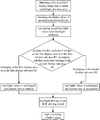
- FIG. 2A is a flowchart of an image display processing method provided by some embodiments of the present disclosure.
- FIG. 2B is a schematic diagram of an example of a first display area and a second display area provided by some embodiments of the present disclosure
- FIG. 2C is a schematic diagram of display data transmission of a display image provided by some embodiments of the present disclosure.
- FIG. 3A is a flowchart of another image display processing method provided by some embodiments of the present disclosure.
- FIG. 3B is a schematic diagram of another example of a first display area and a second display area provided by some embodiments of the present disclosure
- FIG. 4 is a flowchart of an example of acquiring adjusted display data provided by some embodiments of the present disclosure
- FIG. 5 is a curve fit diagram of adjusted display data and compensated display data provided by some embodiments of the present disclosure
- FIG. 6 is a flowchart of an example of an image display processing method provided by some embodiments of the present disclosure.
- FIG. 7 is a schematic block diagram of an example of an image display processing method provided by some embodiments of the present disclosure.
- FIG. 8 is a schematic diagram of still another example of a first display area and a second display area provided by some embodiments of the present disclosure.
- FIG. 9 is a flowchart of another example of acquiring adjusted display data provided by some embodiments of the present disclosure.
- FIG. 10 is a flowchart of still another image display processing method provided by some embodiments of the present disclosure.
- FIG. 11 is a schematic diagram of a display effect of a display image provided by some embodiments of the present disclosure.
- FIG. 12 is a schematic block diagram of an image display processing device provided by some embodiments of the present disclosure.
- FIG. 13 is a schematic block diagram of another image display processing device provided by some embodiments of the present disclosure.
- FIG. 14 is a schematic block diagram of a display device provided by some embodiments of the present disclosure.
- FIG. 15 is a schematic diagram of a non-volatile storage medium provided by some embodiments of the present disclosure.
- connection are not intended to define a physical connection or mechanical connection, but may include an electrical connection, directly or indirectly.
- “On,” “under,” “right,” “left” and the like are only used to indicate relative position relationship, and when the absolute position of the object which is described is changed, the relative position relationship may be changed accordingly.
- a liquid crystal display panel includes a liquid crystal panel and a backlight unit.
- a liquid crystal panel includes an array substrate and an opposite substrate (for example, a color filter substrate) disposed opposite to each other to form a liquid crystal cell, and a liquid crystal layer is filled between the array substrate and the opposite substrate in the liquid crystal cell.
- a first polarizer is on the array substrate, and a second polarizer is on the opposite substrate, and a polarization direction of the first polarizer is perpendicular to a polarization direction of the second polarizer, for example.
- the backlight unit is on a non-display side of the liquid crystal panel for providing a planar light source for the liquid crystal panel.
- the liquid crystal panel comprises a sub-pixel array, and the sub-pixel array comprises a plurality of rows and a plurality of columns, which form a regular matrix (m rows*n columns, and m and n are positive integers), for example.
- Each sub-pixel comprises a switching element, a pixel electrode, and a common electrode.
- the switching element is electrically connected to a gate line in a row, in which the sub-pixel is located, and to a data line in a column, in which the sub-pixel is located. And the switching element is also electrically connected to the pixel electrode. Under control of a scan signal on the gate line, the switching element is turned on, thereby transferring a data signal applied on the data line to the pixel electrode to charge the pixel electrode.
- Liquid crystal molecules of the liquid crystal layer are twisted under an action of a driving electric field formed between a pixel electrode on the array substrate and a common electrode on the array substrate or a common electrode on the opposite substrate, thereby controlling a polarization direction of light passing through the liquid crystal layer, and transmittance of the light is controlled by the cooperation of the first polarizer and the second polarizer, thereby achieving grayscale display.
- the backlight unit may be a direct-lit backlight unit or a side-lit backlight unit.
- a direct-lit backlight unit includes a plurality of point light sources (for example, light-emitting diodes (LEDs)) arranged side by side and a diffusion plate. Light emitted by the point light sources is homogenized by the diffusion plate, and then incident on the liquid crystal panel for display.
- LEDs light-emitting diodes
- high-resolution liquid crystal display panels are also gradually applied to VR devices.
- a VR device because the human eyes are relatively close to a display screen, the human eyes are easier to perceive a display effect of a display image, and therefore, the requirements for a resolution and a display quality of the display panel are also getting higher and higher.
- the direct-lit backlight unit can be controlled by local dimming (LD) technology, so as to improve the display quality of the display panel.
- LD local dimming
- the local dimming technology can not only reduce power consumption of the display panel, but also achieve dynamic dimming of a backlight area, thus greatly improving the contrast of a display image and improving the display quality of the display panel.
- the local dimming technology can divide an entire backlight unit into a plurality of backlight blocks which can be driven individually, and each of the plurality of backlight blocks includes one or more LEDs.
- the local dimming technology can separately control and adjust the light intensity of the plurality of backlight blocks. For example, according to gray scales that need to be displayed in different parts of the display screen, driving currents of the LEDs of the backlight blocks corresponding to these parts are automatically adjusted, so that brightness of each block in the backlight unit is separately adjusted, thereby improving the contrast of the display screen.
- the local dimming technology is generally only applicable to the direct-lit backlight unit, and a plurality of LEDs as the light sources are evenly distributed throughout an entire backplane, for example.
- FIG. 1A a schematic diagram of dividing regions of the LED light sources in the entire backplane is shown in FIG. 1A .
- a small square as shown in FIG. 1A represents an LED unit, and a plurality of regions separated by broken lines represent a plurality of backlight blocks.
- Each of the plurality of backlight blocks includes one or more LED units and can be controlled independently of other backlight blocks.
- the LEDs in each of the plurality of backlight blocks are linked, for example, connected in series, that is, currents passing through the LEDs located in the same backlight block are consistent, so that the luminance brightness is substantially the same.
- FIG. 1B is a schematic diagram of an exemplary system for performing local dimming processing on the backlight unit as shown in FIG. 1A .
- the system is implemented by a hardware circuitry.
- the system includes, for example, a DC power supply 10 , a TCON (Timer Control Register)/SOC (System On Chip) 11 , an FPGA (Field-Programmable Gate Array)/SOC/TCON 12 , and an LED drive circuit board 13 for driving the LEDs to emit light.
- a DC power supply 10 a DC power supply 10
- TCON Timer Control Register
- SOC System On Chip
- FPGA Field-Programmable Gate Array
- the LED drive circuit board 13 includes a micro-chip unit (MCU) 131 , an LED integrated circuit driving chip 132 , a DC/DC circuit 133 , and a current sampling circuit 134 .
- the LED drive circuit board 13 is configured to process each frame of image signal to obtain processed backlight brightness data of respective backlight blocks, and generate driving currents used for various backlight blocks based on the backlight brightness data.
- the driving currents are output to the corresponding backlight blocks to drive the LEDs in the corresponding backlight blocks to emit light by currents.
- the MCU 131 receives a backlight local control signal (Local Dimming SPI (Serial Peripheral Interface) signal) from the FPGA/SOC/TCON 12 , and the backlight local control signal is used in an “AND” operation (controlling whether the “AND” operation is performed according to an enable signal (BL_EN)) with a brightness modulation signal (DIM_PWM) from the TCON 11 to obtain brightness control signals of the respective backlight blocks. Then, the MCU 131 outputs the brightness control signals to the LED integrated circuit driving chip 132 to implement current control of the LEDs of the respective backlight blocks, thereby controlling the light-emitting brightness of the respective backlight blocks.
- a backlight local control signal Local Dimming SPI (Serial Peripheral Interface) signal
- BL_EN enable signal
- DIM_PWM brightness modulation signal
- the system of performing the local dimming process is powered by an external DC power source 10 , and the supply voltage Vin of the power source 10 is typically 24 voltages (V).
- the DC/DC circuit 133 can employ a voltage conversion circuit (e.g., a Boost circuit) to boost the supply voltage Vin to a driving voltage required by illuminating the LEDs of the respective backlight blocks.
- a voltage conversion circuit e.g., a Boost circuit
- the LEDs in the system can be dimmed by a constant-current control mode.
- cathode electrodes (LED ⁇ ) of the plurality of LEDs connected in series in each of the plurality of backlight blocks are connected to the current sampling circuit 134 to monitor the stability of the currents flowing though LEDs that are driven in real time.
- the current sampling circuit 134 converts the currents flowing through the LEDs into voltage signals and feeds the voltage signals back to the LED integrated circuit driving chip 132 , and then the LED integrated circuit driving chip 132 feeds the voltage signals back to the DC/DC circuit 133 .
- the DC/DC circuit 133 adjusts output voltages input to anode electrodes (LED+) of the LEDs to achieve a steady current effect on the LEDs.
- the converted voltage signals are sampled and the sampled voltage signals are compared to a preset reference voltage.
- the current sampling circuit 134 outputs a control signal to enable the DC/DC circuit 133 reduce the output voltage, thereby reducing the currents flowing through the LEDs; otherwise, the current sampling circuit 134 outputs another control signal to enable the DC/DC circuit 133 boost the output voltage to increase the currents flowing through the LEDs. That is, the current sampling circuit 134 can be used as a negative feedback circuit to achieve the constant-current control to the LEDs to enable the LEDs to work stably.
- Each of the exemplary backlight units illustrated in FIGS. 1A and 1B comprises a plurality of rectangular backlight regions arranged in an array
- the local dimming technology can adjust the brightness and darkness of the corresponding backlight blocks according to gray scales of a screen content displayed on the liquid crystal display panel, for a part with higher brightness (gray scale) of a picture, the brightness of the corresponding backlight blocks is also high; and for a part with a lower brightness of the picture, the brightness of the corresponding backlight blocks is also low, thereby achieving a purpose of reducing backlight power consumption, improving the contrast of the display screen, and enhancing the image quality.
- the visual tracking technology in SmartView technology can be used to determine a gaze area of the user's eyes, high-resolution rendering is only performed on the gaze area of the user's eyes, and low-resolution rendering is performed on areas other than the gaze area, thereby reducing the rendering pressure, reducing the power consumption of the display panel, and improving the contrast of the display panel.
- a low-resolution display image that needs to be rendered can be stretched into a high-resolution display image by the IC drive circuit, and then the high-resolution display image is displayed on the display panel, so that the bandwidth of the image transmission can be reduced to some extent, the frame refresh frequency of the image rendering and the refresh frame rate of the VR system can be improved.
- the VR system by combining SmartView technology with the local dimming technology, the dual effects of reducing backlight power consumption and improving image quality contrast can be achieved.
- FIG. 1C is a schematic drive diagram of an IC drive circuit when SmartView technology is applied.
- the other area is a display area of the low-resolution display image.
- the display area of the high-resolution display image can be driven to display by using a drive circuit that is configured to turn on a single row each time as shown in the left side of FIG. 1C
- the display area of the low-resolution display image can be driven to display by using a four-row turned-on-simultaneous drive circuit as shown in the right side of FIG. 1C .
- pixel units in the display area of high-resolution display image adopts a single-row turned-on-simultaneous driving mode, that is, the driving voltage V drives only one row of pixel units, and therefore, a driving current of the row of pixel units is large;
- pixel units in the display area of low-resolution display image adopts a four-row turned-on-simultaneous driving mode, that is, the driving voltage V drives four rows of pixel units, and therefore, the driving current of each row of pixel units in the display area of low-resolution display image is smaller than the driving current of the row of pixel units in the display area of high-resolution display image, for example, is 1 ⁇ 4 of the driving current of the row of pixel units in the display area of high-resolution display
- At least one embodiment of the present disclosure provides an image display processing method of a display device.
- the display device comprises a display panel and a backlight unit, and the backlight unit comprises a plurality of backlight blocks and is driven in a local dimming mode.
- the image display processing method comprises: determining a first display area and a second display area of the display panel; for a frame display image, obtaining backlight values of the plurality of backlight blocks in a case of displaying the frame display image, and calculating compensated display data of respective pixels of the display panel corresponding to the plurality of backlight blocks based on the backlight values of the plurality of backlight blocks; and adjusting compensated display data of at least one first pixel comprised in the first display area to obtain adjusted display data of the at least one first pixel.
- a display resolution of the first display area is larger than a display resolution of the second display area.
- At least one embodiment of the present disclosure also provides an image display processing device, a display device, and a non-volatile storage medium corresponding to the image display processing method described above.
- the image display processing method provided by the above embodiments of the present disclosure can overcome a problem of uneven display brightness of a display panel due to the SmartView technology, thereby improving the contrast of the display image and the display effect of the screen, and reducing the power consumption of the display panel.
- FIG. 2A is a flowchart of an image display processing method provided by some embodiments of the present disclosure.
- the display device comprises a display panel and a backlight unit, and the backlight unit is on a non-display side of the display panel, comprises a plurality of backlight blocks, and is driven in a local dimming mode.
- the plurality of backlight blocks of the backlight unit may be disposed in an array arrangement as shown in FIG.
- the plurality of backlight blocks of the backlight unit may also be disposed in other manners, for example, in an irregular arrangement manner, and the embodiments of the present disclosure are not limited thereto.
- the display device may be a liquid crystal display (LCD) device, an electronic paper display device, or the like, for example, the display device may be a virtual reality device such as a virtual display helmet or the like.
- the display panel of the display device may be a liquid crystal display panel, an electronic paper display panel, or the like, and the embodiments of the present disclosure are not limited to the specific structure and type of the display panel (for example, a vertical electric field type liquid crystal display panel or a horizontal electric field type liquid crystal display panel).
- the image display processing method of some embodiments of the present disclosure may be implemented in a software manner, loaded and executed by a processor in a display panel, for example, loaded and executed by a graphics processing unit (GPU) in the display panel; or at least part of the image display processing method of some embodiments of the present disclosure may be implemented in software, hardware, firmware, or any combination thereof, so as to solve the problem of uneven display brightness of the display panel and improve the display quality of the screen.
- the graphics processing unit may be an internal component of the display device (for example, an integral form of the VR system), or may be a component of an external device (for example, a computer) of the display device (for example, a split type of the VR system), and the embodiments of the present disclosure are not limited thereto.
- the LCD display device may further comprise a pixel array, a data decoding circuit, a timing controller, a gate driver, a data driver, a storage device (for example, a flash memory or the like), and the like.
- the data decoding circuit receives a display input signal and decodes the display input signal to obtain a display data signal; and the timing controller outputs timing signals to control the gate driver, the data driver, etc., to work synchronously, and can perform gamma correction on the display data signal.
- the processed display data signal is input to the data driver to perform a display operation.
- the image display processing method comprises steps S 110 to S 130 , and the steps S 110 to S 130 of the image display processing method and respective exemplary implementations of the steps S 110 to S 130 are respectively described below.
- Step S 110 determining a first display area and a second display area of the display panel.
- Step S 120 for a frame display image, obtaining backlight values of the plurality of backlight blocks in a case of displaying the frame display image, and calculating compensated display data of respective pixels of the display panel corresponding to the plurality of backlight blocks based on the backlight values of the plurality of backlight blocks.
- Step S 130 adjusting compensated display data of at least one first pixel comprised in the first display area to obtain adjusted display data of the at least one first pixel.
- the first display area is, for example, a display area of a high-resolution image
- the second display area is, for example, a display area of a low-resolution image, that is, a display resolution of the first display area is larger than a display resolution of the second display area.
- the first display area and the second display area may be obtained by a visual tracking technology in SmartView technology.
- FIG. 2B is a schematic diagram of an example of a first display area A and a second display area B provided by some embodiments of the present disclosure, and the specific determination process of the first display area A and the second display area B can be, for example, as follows.
- an image acquisition device comprising a CMOS (complementary metal oxide semiconductor) sensor, a CCD (charge coupled device) sensor, an infrared camera, or the like can be used to acquire image information of the eyeball of the user and image information around the eyeball.
- the image acquisition device can be on a side where the display panel is located, for example, be on a frame of a VR device.
- the acquired images are analyzed by the visual tracking technology to extract a pupil center of the human eye, for example, a Scale-invariant Feature Transform (SIFT) feature extraction algorithm, a Histogram of Oriented Gradient (HOG) feature extraction algorithm, and other algorithms in the field may be used to extract feature points of the pupil, and determine a pupil contour to determine the pupil center, and the embodiments of the present disclosure are not limited thereto.
- SIFT Scale-invariant Feature Transform
- HOG Histogram of Oriented Gradient
- a coordinate (x, y) of a fixation point of the pupil center of the human eye on the display panel 302 can be estimated by a certain mathematical model.
- the first display area A that is, a gaze area of the user, is an area within a certain range centering on the coordinate (x, y) of the fixation point, for example, as shown in FIG.
- the first display area A may be an area centered on the fixation point and respectively having a length and a width of about 15% to 45% of a length and a width of the display area of the display panel 302 viewed by the user, for example, may be an area having a length and a width which are 30% of the length and the width of the display area viewed by the user, and the embodiments of the present disclosure are not limited thereto.
- the first display area and the second display area jointly display one frame of display image.
- a display resolution for example, display data
- the display data can be directly displayed on the display panel; and in a case where the display resolution of the frame display image is different from the physical resolution of the display panel (i.e. the first display area and the second display area), the display resolution of the display image can be adjusted to be the same as the physical resolution of the display panel and then displayed on the display panel.
- the display resolution of the display image is an amount of display data of the display image
- the physical resolution of the display panel refers to an amount of pixels of the display panel.
- the first display area A is a display area centered on the fixation point (x, y) and comprising 1440 rows and 1440 columns of pixels, the following embodiments are the same as those described herein, similar descriptions are not described again, however the embodiments of the present disclosure are not limited thereto.
- the display area further comprises a second display area B, that is, a non-gaze area, located outside the first display area A.
- the gaze area changes as the coordinate of a position of the pupil center (that is, the fixation point of the human eye) change.
- the first display area A is a display area with the boundary as a starting edge and comprising 1440 rows and 1440 columns of pixels.
- a first display image with a display resolution of 1440*1440 and centering on the fixation point is obtained on the software terminal, for example, the first display image is displayed in the first display area A.
- the second display area B is a non-gaze area, in order to reduce the transmission load and unnecessary power consumption, the scene of the second display area B can be displayed in a low-definition mode, for example, the low-definition display can be implemented by using a method of four pixel units in each column corresponding to one display data (for example, by using a four-row turned-on-simultaneous driving mode), and therefore, correspondingly, a second display image having a display resolution of 1080*1080 can be acquired on the software terminal, for example, the second display image is displayed on the display panel.
- an image displayed in the first display area is called the first display image
- an image displayed in the second display area is called the second display image. It should be noted that both the first display image and the second display image belong to one frame display image.
- the acquired first display image 1 having a display resolution of 1440*1440 and the acquired second display image 2 having a display resolution of 1080*1080 are transmitted to corresponding areas of the display panel through an IC drive circuit (for example, a data driver and a gate scan driver), so as to be used for the displaying of display images.
- an IC drive circuit for example, a data driver and a gate scan driver
- the first display area A is not limited to the shape and position as shown in FIG. 2B .
- the first display area A may be a superposition of two gaze areas, for example, a first display area A having a co shape is obtained; in a case where the fixation point of the human eye is at the boundary, the position of the first display area A may also be located around the display panel, and the embodiments of the present disclosure are not limit this.
- a display resolution of a display image may be less than or equal to a physical resolution of the display panel, for example, the physical resolution of the display panel is an integer multiple of the display resolution of the display image, which is not limited by the embodiments of the present disclosure.
- the physical resolution of the display panel is the highest resolution of the display panel and is also the optimal resolution of the display panel.
- the display panel comprises m rows*n columns of pixel units, that is, the physical resolution of the display panel is m*n; for example, the display resolution of the display image indicates that the display image comprises j rows*k columns (for example, j, k are integers larger than 0, and m and n are integer multiples of j and k, respectively) of display data.
- the j rows*k columns of display data included in the display image is transmitted as data signals through the data lines to the corresponding pixel units of the display panel for display.
- the physical resolution of the display panel is 4320*4320 is taken as an example, that is, the display panel comprises 4320 rows of pixel units in a horizontal direction, and comprises 4320 columns of pixel units in a vertical direction, and the embodiments of the present disclosure are not limited thereto.
- the display resolution of the display image is 1080*1080
- the display resolution of the display image is lower than the physical resolution of the display panel
- the higher the display resolution of the display image the better the display effect of the display panel.
- a column of pixel units may be used to correspond to multiple columns of display data, so that the display resolution of the display image is converted to be the same as the physical resolution of the display panel.
- a display area determination unit for determining the first display area A and the second display area B of the display panel may be provided, and the first display area A and the second display area B of the display panel are determined by the display area determination unit;
- the display area determination unit can be implemented by SmartView technology, for example, the display area determination unit can also be implemented by a central processing unit (CPU), a graphics processing unit (GPU), a tensor processing unit (TPU), a field-programmable gate array (FPGA), or other forms of processing unit having data processing capabilities and/or program execution capabilities, and corresponding computer instructions.
- the processing unit may be a general-purpose processor or a dedicated processor, and may be an X86 or ARM architecture based processor, or the like.
- the gray values of the display data of the pixels corresponding to the backlight blocks in respective rows can be separately counted by the histogram. It should be noted that, the gray values of the display data of the pixels corresponding to the backlight blocks in respective rows can also be counted by other statistical methods in the art, which is not limited by the embodiments of the present disclosure.
- gray values at 80% to 90% of the counted gray values, which are sorted in an order from small to large, of the display data of the pixels corresponding to the respective backlight blocks are set as the backlight values of the corresponding backlight blocks, or average values of the gray values of the display data of the pixels corresponding to the respective backlight blocks are set as the backlight values of the corresponding backlight blocks.
- the display data used in calculating the backlight value of the backlight block may be the display data of the pixels in a current frame display image or the display data of the pixels in a previous frame display image, which is not limited in the embodiments of the present disclosure.
- the brightness change between a previous frame display image and a next frame display image of the display image is usually small, especially when the display screen is smooth and continuous.
- the following embodiments are described by taking a case that the display data of the current frame display image is used to calculate the backlight value of each backlight block as an example.
- each backlight block can also be determined according to other methods in the art, and the embodiments of the present disclosure are not limited thereto.
- compensated display data of each pixel in the current frame display image corresponding to each backlight block may be obtained according to the following formula:
- LCD com represent the compensated display data of a pixel in the current frame display image
- LCD ori represents display data before compensation of the pixel
- BL PIX represents an actual backlight value corresponding to the pixel and obtained by a backlight diffusion model
- Hm represents the highest gray scale that the pixel displays
- 2.2 represent the gamma value of the gamma curve of the display panel, however the embodiments of the present disclosure are not limited thereto.
- Hm may take 255 or 1023, etc.
- the specific value of Hm may be determined according to a specific situation (for example, a range of a value of the gray scale signal is, for example, 0 to 255 or 0 to 1023, and the like), and the embodiments of the present disclosure are not limited thereto.
- the embodiments of the present disclosure are described by taking a case that the value of Hm is 255 as an example, the following embodiments are the same as those described herein, and similar descriptions are not described again.
- an actual backlight value of a certain pixel in an area of the display panel corresponding to a backlight block is taken as an example to describe. Because light emitted by respective LEDs in the backlight unit may generate light diffusion, and other phenomena, and therefore, the brightness (that is, the backlight value) of the backlight emitted by the LEDs in different positions in the backlight unit has an effect on the actual backlight brightness (actual backlight value) at the position of the pixel.
- the backlight diffusion models of these LEDs at the position of the pixel needs to be fitted according to the distances of respective LEDs in each backlight block to the pixel and the backlight value of each backlight block, and according to these backlight diffusion models, the actual backlight brightness of the pixel is calculated, thereby obtaining the actual backlight brightness of each pixel corresponding to each backlight block.
- the backlight diffusion models can be actually measured according to methods in the art, and will not be described herein.
- the backlight diffusion model is a mathematical model of the actual backlight value corresponding to each pixel, the backlight value of the corresponding backlight block, and the distances of respective LEDs in respective backlight blocks to the pixel, so that the compensated display data corresponding to each pixel of the plurality of backlight blocks can be calculated based on the backlight values of the plurality of backlight blocks.
- the backlight values of the plurality of backlight blocks and the compensated display data of each pixel of the display panel corresponding to the plurality of backlight blocks may be calculated by an algorithm in the art, and details are not described herein again.
- a display data acquisition unit for acquiring the compensated display data of each pixel may be provided, and the backlight values of the plurality of backlight blocks are acquired by the display data acquisition unit, and the compensated display data of the respective pixels corresponding to the plurality of backlight blocks are calculated based on the backlight values of the plurality of backlight blocks;
- the display data acquisition unit can also be implemented by a central processing unit (CPU), a graphics processing unit (GPU), a tensor processing unit (TPU), a field-programmable gate array (FPGA), or other forms of processing unit having data processing capabilities and/or program execution capabilities, and corresponding computer instructions.
- the display panel adopts a driving mode as shown in FIG. 1C , therefore, for example, the display brightness of the first display area A is larger than the display brightness of the second display area B, resulting in a phenomenon in which the brightness is uneven as shown in FIG. 1D .
- the compensated display data of at least one first pixel included in the first display area A may be reduced to obtain adjusted display data of the at least one first pixel.
- a deflection angle of a liquid crystal layer in the at least one first pixel is decreased, so that the transmittance of the light emitted by the backlight block corresponding to the at least one first pixel can be reduced, thereby reducing the display brightness of the first display area A and improving the display quality of the display panel.
- a first adjustment unit for acquiring adjusted display data of the at least one first pixel may be provided, and the compensated display data of the at least one first pixel included in the first display area A is adjusted by the first adjustment unit to obtain the adjusted display data of the at least one first pixel;
- the first adjustment unit can also be implemented by a central processing unit (CPU), a graphics processing unit (GPU), a tensor processing unit (TPU), a field-programmable gate array (FPGA), or other forms of processing unit having data processing capabilities and/or program execution capabilities, and corresponding computer instructions.
- CPU central processing unit
- GPU graphics processing unit
- TPU tensor processing unit
- FPGA field-programmable gate array
- FIG. 3A is a flowchart of another image display processing method provided by some embodiments of the present disclosure
- FIG. 3B is a schematic diagram of another example of a first display area and a second display area provided by some embodiments of the present disclosure.
- the image display processing method further comprises correspondingly adjusting compensated display data of pixels in the second display area B to further improve the display quality of the display panel.
- the image display processing method further comprises a step S 140 .
- the step S 140 can be described in detail below with reference to FIGS. 3A and 3B .
- Step S 140 adjusting compensated display data of at least one pixel comprised in the second display area to obtain adjusted display data of at least one pixel in the second display area.
- At least one pixel comprised in the second display area B may comprise at least one second pixel comprised in a first display sub-area B 1 and at least one pixel comprised in a second display sub-area B 2 as shown in FIG. 3B .
- at least one pixel comprised in the second display area B may comprise at least one second pixel comprised in a first display sub-area B 1 , at least one third pixel comprised in a third display sub-area B 3 , and at least one pixel comprised in a fourth display sub-area B 4 as shown in FIG. 8 below.
- At least one pixel comprised in the second display sub-area B 2 are all pixels comprised in the second display sub-area B 2
- at least one pixel comprised in the fourth display sub-area B 4 are all pixels comprised in the fourth display sub-area B 4 .
- the second display area B comprises a first display sub-area B 1 and a second display sub-area B 2 .
- the first display sub-area B 1 and the first display area A are in the same row, and have the same row height (for example, the number of rows of sub-pixel rows in the display panel); and the second display sub-area B 2 and the first display area A are in different rows.
- the dashed-line boxes shown in FIG. 3B represent respective backlight blocks corresponding to respective display areas of the display panel.
- a direction of the row in “the same row” or “different rows” in the above description is, for example, the same as a direction of each row in line-by-line scanning process, and the following embodiments are the same and will not be repeated here.
- a row drive circuit used in the first display sub-area B 1 and a row drive circuit used in the first display area A are the same, that is, a drive circuit that is configured to turn on a single row each time as shown in FIG. 1C is used, and therefore, the display brightness of the first display sub-area B 1 and the display brightness of the first display area A are the same, and both are higher than the display brightness of the second display sub-area B 2 .
- adjusting compensated display data at least one pixel comprised in the second display area B comprises: reducing compensated display data of at least one second pixel comprised in the first display sub-area B 1 to obtain the adjusted display data of the at least one second pixel, thereby reducing the display brightness of the first display sub-area B 1 .
- adjusting compensated display data of at least one pixel comprised in the second display area B further comprises: maintaining compensated display data of at least one pixel comprised in the second display sub-area B 2 unchanged.
- the transmittance of the light emitted by the backlight blocks corresponding to the first display area A and the first display sub-area B 1 is reduced, however the compensated display data of the second display sub-area B 2 having the lower display brightness can be kept unchanged, so that the brightness uniformity of the first display area A, the first display sub-area B 1 , and the second display sub-area B 2 is improved, thereby improving the display quality of the display panel.
- a second adjustment unit for acquiring the adjusted display data of at least one pixel in the second display area B may be provided, and the compensated display data of at least one pixel included in the second display area B is adjusted by the second adjustment unit to obtain the adjusted display data of at least one pixel included in the second display area B;
- the second adjustment unit can also be implemented by a central processing unit (CPU), a graphics processing unit (GPU), a tensor processing unit (TPU), a field-programmable gate array (FPGA), or other forms of processing unit having data processing capabilities and/or program execution capabilities, and corresponding computer instructions.
- FIG. 4 is a flowchart of some examples of acquiring adjusted display data provided by some embodiments of the present disclosure. That is, FIG. 4 is a flowchart of some examples of steps S 130 and S 140 as shown in FIG. 3A .
- a method of acquiring the adjusted display data comprises steps S 1411 to S 1412 .
- an image display processing method of an embodiment of the present disclosure will be described with reference to FIG. 4 .
- Step S 1411 obtaining a mapping relationship between adjusted display data of respective pixels of the display panel and compensated display data of the respective pixels of the display panel.
- step S 1411 for example, in 256 gray scale levels (that is, 0-255) corresponding to the respective pixels of the second display sub-area B 2 , at least 35 different gray scale values, for example, are taken at intervals, for example, taking 35 different gray scale values, 50 different gray scale values, and the like, and the embodiments of the present disclosure are not limited thereto.
- the 256 gray scale levels are all compensated display data.
- the compensated display data of the first pixel comprised in the first display area A and the compensated display data of the second pixel comprised in the first display sub-area B 1 are adjusted by enabling the display brightness of the display panel corresponding to the gray scale uniform, and so on, so that adjusted display data, which are in one-to-one correspondence to at least 35 gray scale levels, in the first display area A and in the first display sub-area B 1 can be obtained.
- a two-segment polynomial curve fit is performed based on the at least 35 gray scale levels and the adjusted display data, and a curve fit graph of the adjusted display data and the compensated display data as shown in FIG. 5 can be, for example, obtained.
- the curve fit graph as shown in FIG. 5 is only an example, and the specific curve fit result is determined according to actual conditions, and the embodiments of the present disclosure are not limited thereto.
- the adjusted display data is, for example, 80, that is, the gray scale value is reduced by 20, so as to enable the display brightness of the display panel uniform.
- Step S 1412 acquiring, according to the mapping relationship, the adjusted display data of the at least one first pixel comprised in the first display area and the adjusted display data of the at least one second pixel comprised in the first display sub-area.
- an expression (that is, the mapping relationship) of the two-segment fit curve function as shown in FIG. 5 can be expressed as:
- f (LCD com ) represents adjusted display data of a pixel of the at least one first pixel comprised in the first display area A or adjusted display data of a pixel of the at least one second pixel comprised in the first display sub-area B 1
- LCD com represents compensated display data of the pixel
- a i and b i represent adjustment coefficients of display data in different gray scale ranges
- i is an integer greater than or equal to 0
- the compensated display data of the pixel can be obtained by the formula (1), and repeated portions will be omitted here.
- the compensated display data of the pixels in the first display area A and the first display sub-area B 1 can be adjusted in real time according to the above formula (2), and the adjusted display data is used for driving the corresponding display area of the display panel, so that the display panel reaches the display effect as shown in FIG. 11 , thereby solving the phenomenon as shown in FIG. 1D that the display brightness of the display panel is uneven, and improving the display quality of the display panel.
- FIG. 6 is a flowchart of some examples of an image display processing method provided by some embodiments of the present disclosure
- FIG. 7 is a schematic block diagram of some examples of an image display processing method provided by some embodiments of the present disclosure.
- the image display processing method provided by some embodiments of the present disclosure is systematically described in conjunction with FIG. 6 and FIG. 7 .
- the embodiments of the present disclosure are described by taking a case that the a second display image with a display resolution of 1080*1080 and a first display image with a display resolution of 1440*1440 are input to the display panel with a physical resolution of 4320*4320 as an example, the embodiments of the present disclosure are not limited thereto, for details, the descriptions of FIG. 2B and FIG. 2C can be referred, and the details are not described herein again.
- a second display image having a display resolution of 1080*1080 is acquired.
- backlight values of respective backlight blocks are obtained based on the display image, for example, the backlight values may be applied to the respective backlight blocks in the backlight unit through, for example, the LED drive circuit board as shown in FIG. 1B ;
- the first display area is determined based on the center coordinate (that is, coordinate of the fixation point) (x, y), which is acquired by the SmartView technology, of the gaze point of the human eye in the display panel, for example, the first display area A (as shown in FIG. 2B ) centered on the center coordinate (x, y) and comprising 1440 rows and 1440 columns of pixels and a high-resolution display image having a display resolution of 1440*1440 displayed in the first display area A are obtained.
- a backlight diffusion model is obtained based on the backlight values of the respective backlight blocks obtained by the above calculation, and actual backlight values after backlight in each backlight block is diffused are acquired based on the backlight diffusion model, so that the compensated display data of respective pixels of the display panel corresponding to each backlight block are acquired by formula (1) based on the actual backlight values.
- each pixel of the display image belongs to the first display area A or the first display sub-area B 1 as shown in FIG. 3B , or it is judged whether each pixel of the display image belongs to the second display sub-area B 2 as shown in FIG. 3B .
- the pixel belongs to the first display area A or the first display sub-area B 1 , the backlight values of the respective backlight blocks are kept unchanged, and the compensated display data of the first pixel or the second pixel in the display area is reduced.
- the reduced compensated display data can be obtained by the formula (2), that is, the adjusted display data is obtained.
- the adjusted display data is used to drive the first display area A or the first display sub-area B 1 in the display panel to display by, for example, the drive circuit that is configured to turn on a single row each time as shown in a left diagram of FIG. 1C .
- the compensated display data of at least one pixel comprised in the second display sub-area B 2 is kept unchanged, and the compensated display data is used to drive the second display sub-area B 2 in the display panel to display by, for example, the four-row turned-on-simultaneous drive circuit as shown in a right diagram of FIG. 1C .
- a high-resolution display image having a display resolution of 1440*1440 can be displayed on the first display area A in the display panel, a low-resolution display image is displayed in the second display area B, so that the display panel reaches the display effect as shown in FIG. 11 , thereby solving the phenomenon that the display brightness of the display panel as shown in FIG. 1D is uneven, and improving the display quality of the display panel.
- step S 140 there are different adjustment methods for the compensated display data of a plurality of sub-pixels comprised in the second display area B according to different division methods of respective sub-areas of the second display area B.
- FIG. 8 is a schematic diagram of still another example of a first display area and a second display area provided by some embodiments of the present disclosure
- FIG. 9 is a flowchart of another method for acquiring adjusted display data provided by some embodiments of the present disclosure. That is, FIG. 9 is a flowchart of still other examples of steps S 130 and S 140 as shown in FIG. 3A .
- the method for acquiring adjusted display data comprises steps S 1421 to S 1424 .
- an image display processing method of an embodiment of the present disclosure will be described with reference to FIG. 9 .
- Step S 1421 reducing backlight values of a plurality of rows of backlight blocks corresponding to the first display area, the first display sub-area, and the third display sub-area, respectively.
- Step S 1422 according to the backlight values of the plurality of rows of backlight blocks corresponding to the first display area, the first display sub-area, and the third display sub-area respectively, acquiring the compensated display data of the at least one first pixel comprised in the first display area, the compensated display data of the at least one second pixel comprised in the first display sub-area, and compensated display data of at least one third pixel comprised in the third display sub-area again.
- Step S 1423 increasing the compensated display data of the at least one third pixel comprised in the third display sub-area to obtain adjusted display data of the at least one third pixel comprised in the third display sub-area.
- Step S 1424 reducing the compensated display data of the at least one first pixel comprised in the first display area and the compensated display data of the at least one second pixel comprised in the first display sub-area, to obtain adjusted display data of the at least one first pixel comprised in the first display area and adjusted display data of the at least one second pixel comprised in the first display sub-area.
- the second display sub-area B 2 further comprises a third display sub-area B 3 and a fourth display sub-area B 4 .
- the third display sub-area B 3 and a boundary portion, which is adjacent to the second display sub-area B 2 , in the first display area A and the first display sub-area B 1 correspond to a same row of backlight blocks (for example, as shown in FIG. 8 , correspond to the same row of dotted-line boxes).
- the fourth display sub-area B 4 and the boundary portion, which is adjacent to the second display sub-area B 2 , in the first display area A and the first display sub-area B 1 correspond to different backlight blocks, respectively.
- the backlight values of the backlight blocks and the compensated display data of the corresponding display areas can be simultaneously adjusted to improve the uniformity of the display brightness of the display panel.
- the backlight values of the plurality of rows of backlight blocks respectively corresponding to the first display area A and the first display sub-area B 1 may be reduced. Because the third display sub-area B 3 and a boundary portion, which is adjacent to the third display sub-area B 3 , in the first display area A and the first display sub-area B 1 are located in the same row of backlight blocks, that is, the backlight values of the backlight blocks corresponding to the third display sub-area B 3 are also reduced.
- step S 1422 because the compensated display data of each display area is obtained based on the backlight values according to the formula (1), and therefore, in a case where the backlight values corresponding to the respective display areas are changed in step S 1421 , the compensated display data of the respective display areas needs to be determined again.
- the specific process may be referred to the related description in step S 120 , and details are not described herein again.
- step S 1423 because the display brightness of the third display sub-area B 3 is relatively low, in a case where the backlight values of the plurality of rows of the backlight blocks respectively corresponding to the first display area A and the first display sub-area B 1 , which have higher display brightness, are reduced in the step S 1421 , because the third display sub-area B 3 and the boundary portion, which is adjacent to the third display sub-area B 3 , in the first display area A and the first display sub-area B 1 are located in the same row of backlight blocks, therefore, while reducing the display brightness of the first display area A and the display brightness of the first display sub-area B 1 , the backlight values of the backlight blocks corresponding to the third display sub-area B 3 are also reduced, so that after the compensated display data of the third display sub-area B 3 is calculated in step S 1422 , in order to increase the display brightness of the third display sub-area B 3 to enable the display brightness of the display panel more uniform, therefore,
- a mapping relationship or a fit curve between the adjusted display data of the third pixel comprised in the third display sub-area B 3 and the compensated display data of the third pixel comprised in the third display sub-area B 3 may be re-determined according to the relevant introduction in step S 1411 , so as to determine the adjusted display data of the third pixel of the third display sub-area B 3 according to the mapping relationship or the fit curve, and details are not described herein again.
- the adjusted display data of the first pixel comprised in the first display area and the adjusted display data of the second pixel comprised in the first display sub-area may be calculated based on the formula (2) determined in the step S 1411 , the specific process may be referred to the step S 1411 , and details are not described herein again.
- Some embodiments of the present disclosure also provides another image display processing method. As shown in FIG. 10 , on the basis of the example as shown in FIG. 2A or FIG. 3A , the image display processing method further comprises steps S 150 to S 170 .
- the image display processing method further comprises steps S 150 to S 170 .
- an image display processing method of an embodiment of the present disclosure will be described with reference to FIG. 10 .
- Step S 150 transmitting the backlight values of the plurality of backlight blocks to the backlight unit.
- Step S 160 transmitting the adjusted display data of the at least one first pixel comprised in the first display area and the adjusted display data of the at least one second pixel comprised in the first display sub-area to the display panel through a drive circuit that is configured to turn on a single row each time.
- Step S 170 transmitting adjusted display data of at least one pixel comprised in the second display sub-area to the display panel through a drive circuit that is configured to turn on rows each time, to perform a display operation of the display panel.
- the backlight values of the respective backlight blocks are input to, for example, a LED drive circuit board 13 as shown in FIG. 1B .
- the LED drive circuit board 13 generates drive currents for the respective backlight blocks based on the backlight values of the respective backlight blocks, and outputs the drive currents to the corresponding backlight blocks to control the LEDs in these backlight blocks to emit light through the currents.
- the adjusted display data is transmitted to a data driver of the display panel and transmitted to the corresponding pixel of the display panel through the data driver.
- the pixels comprised in the first display area and the first display sub-area in the display panel are turned on row by row under drive of, for example, a gate scan signal outputted by a drive circuit that is configured to turn on a single row each time as shown in left diagram of FIG. 1C , to control the deflection of the liquid crystal molecules of the liquid crystal layer in the corresponding pixel in the display panel according to the adjusted display data transmitted by the data driver, so that the light emitted by the backlight unit is transmitted, thereby displaying the display image on the display panel.
- every four rows of the pixels comprised in the second display area in the display panel are turned on simultaneously under drive of, for example, gate scan signals outputted by a four-row turned-on-simultaneous drive circuit as shown in the right diagram of FIG. 1C , to control the deflection of the liquid crystal molecules of the liquid crystal layer in the corresponding pixel in the display panel according to the adjusted display data transmitted by the data driver, so that the light emitted by the backlight unit is transmitted, thereby displaying the display image on the display panel.
- the flowchart of the image display processing method provided by some embodiments of the present disclosure may comprise more or less operations, and the operations may be performed sequentially or in parallel.
- the flowchart of the image display processing method described above comprises a plurality of operations occurring in a specific order, it should be clearly understood that, the order of the plurality of operations is not limited.
- the image display processing method described above may be performed once or may be performed a plurality of times according to predetermined conditions.
- FIG. 12 is a schematic block diagram of an image display processing device provided by some embodiments of the present disclosure.
- the image display processing device 100 comprises a display area determination unit 110 , a display data acquisition unit 120 , and a first adjustment unit 130 .
- these units may be implemented in the form of hardware (such as, circuits) modules or software modules, and any combination thereof.
- the display area determination unit 110 is configured to determine a first display area and a second display area of the display panel. For example, a display resolution of the first display area is larger than a display resolution of the second display area.
- the display data acquisition unit 120 is configured to obtain backlight values of the plurality of backlight blocks, and calculate compensated display data of respective pixels of the display panel corresponding to the plurality of backlight blocks based on the backlight values of the plurality of backlight blocks.
- the first adjustment unit 130 is configured to adjust compensated display data of at least one first pixel comprised in the first display area to obtain adjusted display data of the at least one first pixel.
- the image display processing device 100 further comprises a second adjustment unit (not shown in the drawing).
- the second adjustment unit is configured to adjust compensated display data of at least one pixel comprised in the second display area to obtain adjusted display data of at least one pixel in the second display area.
- the image display processing device may comprise more or fewer circuits or units, and the connection relationship among the respective circuits or units is not limited and may be determined according to actual needs.
- the specific configuration of each circuit is not limited, and may include an analog device according to the circuit principle, may also include digital chips, or other suitable manners.
- FIG. 13 is a schematic block diagram of another image display processing device provided by some embodiments of the present disclosure.
- the image display processing device 200 comprises a processor 210 , a memory 220 , and one or more computer program modules 221 .
- the processor 210 is connected with the memory 220 by a bus system 230 .
- the one or more computer program modules 221 are stored in the memory 220 .
- the one or more computer program modules 221 include instructions that are executable by a computer used for achieving the image display processing method provided by any one of the embodiments of the present disclosure.
- the instructions of the one or more computer program modules 221 can be executed by the processor 210 .
- the bus system 230 is a serial or parallel communication bus, etc., and no limitation is imposed in this aspect in the embodiments of the present disclosure.
- the processor 210 may be a central processing unit (CPU), a field programmable logic gate array (FPGA), or other processing units with a data processing ability and/or instruction execution ability.
- the processor 210 may be a general processor or a dedicated processor, and can control other components in the image display processing device 200 to achieve the expected functions.
- the memory 220 can include one or more computer program products, and the computer program products includes a computer-readable storage media in various forms, for example, includes a volatile storage and/or a non-volatile storage.
- the volatile storage for example, includes a random access memory (RAM) and/or a cache memory, etc.
- the non-volatile storage for example, includes a read-only memory (ROM), a hard disk, and a flash memory, etc.
- One or more computer program instructions can be stored in the computer-readable storage medium, and the processor 210 can run or execute the program instructions to achieve the functions (which are to be achieved by the processor 210 ) in the embodiments of the present disclosure and/or other expected functions, such as an image display processing method, etc.
- Various applications and data such as a coordinate of the fixation point (x, y) and various data used and/or generated by application programs, etc., can also be stored in the computer-readable storage medium.
- the embodiment of the present disclosure does not illustrate all components of the image display processing device 200 .
- Those skilled in the art can provide and arrange other components, which are not illustrated in the figures, of the image display processing device 200 according to actual requirements to achieve necessary functions of the image display processing device 200 , and the embodiment of the present disclosure is not limited thereto.
- FIG. 14 is a schematic block diagram of a display device provided by some embodiments of the present disclosure.
- a display device 300 comprises a display panel 302 , a backlight unit 303 , and an image display processing device 301 provided by any one embodiment of the present disclosure.
- the backlight unit 303 comprises a plurality of backlight blocks and is driven in a local dimming mode.
- the image display processing device 301 may be the image display processing device 100 as shown in FIG. 12 or the image display processing device 200 as shown in FIG. 13 , and the embodiments of the present disclosure are not limited thereto.
- the image display processing device 301 generates backlight values and adjusted display data.
- the backlight values for example, are transmitted to an LED drive circuit board in the backlight unit 303 , thereby controlling LEDs in a corresponding backlight block of the backlight unit to emit light;
- the adjusted display data is transmitted to, for example, a drive chip (not shown in the drawing, for example, a data drive circuit) in the display panel 302 to control the deflection of the liquid crystal molecules of the liquid crystal layer in the display panel, so that the light emitted by the backlight unit 303 is transmitted, thereby displaying a display image on the display panel 302 .
- the display device 300 may be a thin film transistor liquid crystal display device, an electronic paper display device, or the like.
- the display device is a VR device, such as a VR helmet or the like, and the embodiments of the present disclosure are not limited to this case.
- these components are interconnected by a bus system and/or other coupling mechanisms (not shown in figures).
- the bus system may be a conventional serial, parallel communication bus, etc., and the embodiments of the present disclosure are not limit to this case.
- the components and structures of the display device 300 as shown in FIG. 14 are merely exemplary and not limiting, and the display device 300 may include other components and structures as needed.
- FIG. 15 is a schematic diagram of a non-volatile storage medium provided by some embodiments of the present disclosure.
- the non-volatile storage medium 400 non-temporarily stores computer readable instructions 401
- the image display processing method provided by any one of the embodiments of the present disclosure may be performed when the non-volatile computer readable instructions 401 are executed by a computer (comprising a processor).
- the non-volatile storage medium may be any combination of one or more computer-readable storage media.
- one computer-readable storage medium includes computer-readable program codes used for determining the compensated display data
- another computer-readable storage medium includes computer-readable program codes used for obtaining the adjusted display data.
- the program codes are read by the computer
- the program codes stored in the computer-readable storage medium are executed by the computer, and for example, the image display processing method provided by any one of the embodiments of the present disclosure is performed.
- the non-volatile storage medium may include a memory card of a smart phone, a storage component of a tablet, a hard disk of a personal computer, a random access memory (RAM), a read-only memory (ROM), an erasable programmable read-only memory (EPROM), a portable compact disk read-only memory (CD-ROM), a flash memory, or any combination of the above-mentioned storage media, may also be other suitable storage media.
- RAM random access memory
- ROM read-only memory
- EPROM erasable programmable read-only memory
- CD-ROM portable compact disk read-only memory
- flash memory or any combination of the above-mentioned storage media, may also be other suitable storage media.
Landscapes
- Engineering & Computer Science (AREA)
- Physics & Mathematics (AREA)
- Computer Hardware Design (AREA)
- General Physics & Mathematics (AREA)
- Theoretical Computer Science (AREA)
- Chemical & Material Sciences (AREA)
- Crystallography & Structural Chemistry (AREA)
- Control Of Indicators Other Than Cathode Ray Tubes (AREA)
- Liquid Crystal Display Device Control (AREA)
Abstract
Description
where f (LCDcom) represents adjusted display data of a pixel of the at least one first pixel comprised in the first display area or adjusted display data of a pixel of the at least one second pixel comprised in the first display sub-area, LCDcom represents compensated display data of the pixel, ai and bi represent adjustment coefficients of display data in different gray scale ranges, Hm represents a highest gray scale displayed by the pixel, i is an integer greater than or equal to 0 and less than or equal to n, and n is an integer greater than 1.
where LCDori represents display data before compensation of the pixel, and BLPIX represents an actual backlight value corresponding to the pixel and obtained by a backlight diffusion model.
where, LCDcom represent the compensated display data of a pixel in the current frame display image, LCDori represents display data before compensation of the pixel, BLPIX represents an actual backlight value corresponding to the pixel and obtained by a backlight diffusion model, Hm represents the highest gray scale that the pixel displays, and 2.2 represent the gamma value of the gamma curve of the display panel, however the embodiments of the present disclosure are not limited thereto.
where f (LCDcom) represents adjusted display data of a pixel of the at least one first pixel comprised in the first display area A or adjusted display data of a pixel of the at least one second pixel comprised in the first display sub-area B1, LCDcom represents compensated display data of the pixel, ai and bi represent adjustment coefficients of display data in different gray scale ranges, i is an integer greater than or equal to 0 and less than or equal to n, and n is an integer greater than 1.
Claims (19)
Applications Claiming Priority (3)
| Application Number | Priority Date | Filing Date | Title |
|---|---|---|---|
| CN201910151384.X | 2019-02-28 | ||
| CN201910151384.XA CN109658876B (en) | 2019-02-28 | 2019-02-28 | Image display processing method and device, display device and storage medium |
| CN201910151384 | 2019-02-28 |
Publications (2)
| Publication Number | Publication Date |
|---|---|
| US20200279534A1 US20200279534A1 (en) | 2020-09-03 |
| US10878761B2 true US10878761B2 (en) | 2020-12-29 |
Family
ID=66123357
Family Applications (1)
| Application Number | Title | Priority Date | Filing Date |
|---|---|---|---|
| US16/558,916 Active US10878761B2 (en) | 2019-02-28 | 2019-09-03 | Image display processing method and device, display device, and non-volatile storage medium |
Country Status (2)
| Country | Link |
|---|---|
| US (1) | US10878761B2 (en) |
| CN (1) | CN109658876B (en) |
Families Citing this family (41)
| Publication number | Priority date | Publication date | Assignee | Title |
|---|---|---|---|---|
| EP3933823A1 (en) * | 2019-02-27 | 2022-01-05 | Boe Technology Group Co., Ltd. | Image display processing method and apparatus, display apparatus, and storage medium |
| CN114387883B (en) * | 2019-04-30 | 2023-09-29 | 武汉天马微电子有限公司 | A display device and electronic equipment |
| CN112150972B (en) * | 2019-06-28 | 2022-05-06 | 华为技术有限公司 | Image compensation method and device, and display device |
| TWI707334B (en) * | 2019-09-03 | 2020-10-11 | 佳世達科技股份有限公司 | Display device |
| CN110634434B (en) * | 2019-09-11 | 2022-08-05 | 武汉天马微电子有限公司 | Driving method and driving device of display panel and display device |
| CN110767142B (en) * | 2019-09-12 | 2023-05-23 | 苏州佳世达电通有限公司 | Display apparatus |
| CN113243030B (en) * | 2019-09-26 | 2022-07-12 | 京东方科技集团股份有限公司 | Image processing method and device |
| CN110648640B (en) * | 2019-09-27 | 2021-07-16 | 厦门天马微电子有限公司 | Pixel compensation method, pixel compensation device and display device |
| CN112581874B (en) * | 2019-09-29 | 2022-09-23 | 北京小米移动软件有限公司 | Display panel, display device, display control method, device and terminal equipment |
| US10909937B1 (en) * | 2019-11-18 | 2021-02-02 | Novatek Microelectronics Corp. | Driver circuit and related display system |
| CN110853566B (en) * | 2019-11-29 | 2023-06-13 | 京东方科技集团股份有限公司 | Driving method of silicon-based driving backboard and display device |
| CN113748378B (en) * | 2020-03-27 | 2023-10-13 | 京东方科技集团股份有限公司 | Alignment deviation detection method and device, data compensation method and device |
| CN114071150B (en) * | 2020-07-31 | 2023-06-16 | 京东方科技集团股份有限公司 | Image compression method and device, image display method and device and medium |
| CN114067757B (en) * | 2020-07-31 | 2023-04-14 | 京东方科技集团股份有限公司 | Data processing method and device, display device |
| KR20220021961A (en) * | 2020-08-13 | 2022-02-23 | 삼성전자주식회사 | Electronic device and operating method of electronic device |
| US11410580B2 (en) | 2020-08-20 | 2022-08-09 | Facebook Technologies, Llc. | Display non-uniformity correction |
| KR102887684B1 (en) | 2020-08-25 | 2025-11-19 | 엘지디스플레이 주식회사 | Display device and electric device including the same |
| CN114120898B (en) * | 2020-08-31 | 2023-02-24 | 北京小米移动软件有限公司 | Brightness adjustment method, brightness adjustment device, and computer-readable storage medium |
| US11281047B1 (en) * | 2020-12-01 | 2022-03-22 | Solomon Systech (China) Limited | Backlight generation with local dimming for liquid crystal panel having arbitrary shape |
| WO2022134008A1 (en) * | 2020-12-25 | 2022-06-30 | 京东方科技集团股份有限公司 | Image display method, apparatus, electronic device and storage medium |
| US11733773B1 (en) * | 2020-12-29 | 2023-08-22 | Meta Platforms Technologies, Llc | Dynamic uniformity correction for boundary regions |
| CN112863453B (en) * | 2021-01-07 | 2022-07-12 | Tcl华星光电技术有限公司 | Holographic display method and holographic display system |
| CN114792502B (en) * | 2021-01-26 | 2025-04-08 | 京东方科技集团股份有限公司 | Pixel data compensation device and method, display panel and storage medium |
| CN112967688B (en) * | 2021-03-15 | 2022-03-01 | 四川长虹电器股份有限公司 | Method and device for improving contrast of liquid crystal display television of multi-partition backlight system |
| CN113077762A (en) * | 2021-03-17 | 2021-07-06 | Tcl华星光电技术有限公司 | Driving method and driving circuit of Mini LED backlight module and display device |
| US11681363B2 (en) | 2021-03-29 | 2023-06-20 | Meta Platforms Technologies, Llc | Waveguide correction map compression |
| CN115699156A (en) | 2021-05-25 | 2023-02-03 | 京东方科技集团股份有限公司 | Control method for display panel, control device for display panel and display device |
| US11651744B2 (en) * | 2021-10-14 | 2023-05-16 | Dell Products L.P. | Systems and methods for increasing backlight uniformity for backlit display panels |
| KR102907286B1 (en) * | 2021-10-18 | 2026-01-02 | 엘지디스플레이 주식회사 | Gamma voltage generating circuit and display device including the same |
| CN114023273B (en) | 2021-11-22 | 2023-03-21 | 深圳创维-Rgb电子有限公司 | Local dimming driving circuit, method and system and electronic equipment |
| US11754846B2 (en) | 2022-01-21 | 2023-09-12 | Meta Platforms Technologies, Llc | Display non-uniformity correction |
| CN114677988B (en) * | 2022-04-27 | 2023-05-30 | 广州华星光电半导体显示技术有限公司 | Brightness compensation method and device for display panel |
| CN114974063B (en) * | 2022-05-05 | 2025-06-27 | 武汉华星光电半导体显示技术有限公司 | Display panel and gray level compensation method |
| CN114999376A (en) * | 2022-06-30 | 2022-09-02 | 重庆翰博显示科技研发中心有限公司 | A display method for virtual reality equipment |
| CN115657367B (en) * | 2022-10-19 | 2024-01-05 | 长春希达电子技术有限公司 | High-partition dynamic dimming method for LED backlight module |
| CN115691394A (en) * | 2022-11-16 | 2023-02-03 | 昆山国显光电有限公司 | Display compensation method, device, equipment, display device and storage medium |
| CN115938263A (en) * | 2022-11-28 | 2023-04-07 | 北京京东方显示技术有限公司 | Display panel, control method and display device |
| CN116741108A (en) * | 2023-03-31 | 2023-09-12 | 惠科股份有限公司 | Side-entering type backlight module, control method thereof and display device |
| CN116189558B (en) * | 2023-04-28 | 2023-07-11 | 惠科股份有限公司 | Display device and display method thereof |
| CN117930731B (en) * | 2024-03-21 | 2024-07-12 | 成都凯天电子股份有限公司 | Control method and system for display of liquid crystal display instrument |
| CN119626096B (en) * | 2024-09-09 | 2026-02-10 | 北京京东方显示技术有限公司 | Display module, display method, controller, storage medium and display system |
Citations (9)
| Publication number | Priority date | Publication date | Assignee | Title |
|---|---|---|---|---|
| US20030184561A1 (en) * | 2002-03-29 | 2003-10-02 | The Boeing Company | Gaze directed visual system |
| JP2004029141A (en) | 2002-06-21 | 2004-01-29 | Mitsubishi Electric Corp | Back light source for display device, liquid crystal display device, and method of adjusting back light source |
| CN103295553A (en) | 2013-06-26 | 2013-09-11 | 青岛海信信芯科技有限公司 | Direct type backlight luminance compensation method and display device |
| CN103403607A (en) | 2011-03-04 | 2013-11-20 | 三星电子株式会社 | Multiple viewpoint image display device |
| US20150348469A1 (en) * | 2013-01-22 | 2015-12-03 | Sharp Kabushiki Kaisha | Liquid crystal display device |
| US20170365230A1 (en) * | 2017-09-05 | 2017-12-21 | Darwin Hu | Display devices showing multimedia in multiple resolutions with eye tracking |
| CN109192126A (en) | 2018-10-10 | 2019-01-11 | 深圳市华星光电技术有限公司 | The image processing method of display panel |
| CN109388448A (en) | 2017-08-09 | 2019-02-26 | 京东方科技集团股份有限公司 | Image display method, display system and computer readable storage medium |
| US20200051512A1 (en) * | 2018-08-09 | 2020-02-13 | Beijing Boe Optoelectronics Technology Co., Ltd. | Image display processing method and device, display device and non-volatile storage medium |
-
2019
- 2019-02-28 CN CN201910151384.XA patent/CN109658876B/en active Active
- 2019-09-03 US US16/558,916 patent/US10878761B2/en active Active
Patent Citations (10)
| Publication number | Priority date | Publication date | Assignee | Title |
|---|---|---|---|---|
| US20030184561A1 (en) * | 2002-03-29 | 2003-10-02 | The Boeing Company | Gaze directed visual system |
| JP2004029141A (en) | 2002-06-21 | 2004-01-29 | Mitsubishi Electric Corp | Back light source for display device, liquid crystal display device, and method of adjusting back light source |
| CN103403607A (en) | 2011-03-04 | 2013-11-20 | 三星电子株式会社 | Multiple viewpoint image display device |
| US20130335538A1 (en) | 2011-03-04 | 2013-12-19 | Samsung Electronics Co., Ltd. | Multiple viewpoint image display device |
| US20150348469A1 (en) * | 2013-01-22 | 2015-12-03 | Sharp Kabushiki Kaisha | Liquid crystal display device |
| CN103295553A (en) | 2013-06-26 | 2013-09-11 | 青岛海信信芯科技有限公司 | Direct type backlight luminance compensation method and display device |
| CN109388448A (en) | 2017-08-09 | 2019-02-26 | 京东方科技集团股份有限公司 | Image display method, display system and computer readable storage medium |
| US20170365230A1 (en) * | 2017-09-05 | 2017-12-21 | Darwin Hu | Display devices showing multimedia in multiple resolutions with eye tracking |
| US20200051512A1 (en) * | 2018-08-09 | 2020-02-13 | Beijing Boe Optoelectronics Technology Co., Ltd. | Image display processing method and device, display device and non-volatile storage medium |
| CN109192126A (en) | 2018-10-10 | 2019-01-11 | 深圳市华星光电技术有限公司 | The image processing method of display panel |
Non-Patent Citations (1)
| Title |
|---|
| Chinese Office Action in Chinese Application No. 201910151384.X, dated Mar. 10, 2020 with English translation. |
Also Published As
| Publication number | Publication date |
|---|---|
| US20200279534A1 (en) | 2020-09-03 |
| CN109658876B (en) | 2023-04-11 |
| CN109658876A (en) | 2019-04-19 |
Similar Documents
| Publication | Publication Date | Title |
|---|---|---|
| US10878761B2 (en) | Image display processing method and device, display device, and non-volatile storage medium | |
| US10984736B2 (en) | Image display processing method and device thereof, display device and storage medium | |
| US11521564B2 (en) | Image display processing method and device, display device and non-volatile storage medium | |
| US10923046B2 (en) | Image display processing method and device, display device and non-volatile storage medium | |
| US11244636B2 (en) | Display device comprising backlight unit with backlight blocks in rows driven by local dimming method | |
| US11222607B2 (en) | Display driving method, driving device, and display device comprising display panel and backlight unit | |
| US11270657B2 (en) | Driving method, driving apparatus, display device and computer readable medium | |
| US11380271B2 (en) | Backlight driving method, display driving method, drive device and display device | |
| CN109147688B (en) | Display panel data voltage control method, display panel and display device | |
| US10872558B2 (en) | Image display processing method and device, display device and non-volatile storage medium | |
| KR101543277B1 (en) | Method of driving light source | |
| US12148399B2 (en) | Display device and driving method thereof | |
| WO2020000508A1 (en) | Control circuit of liquid crystal display panel and liquid crystal display panel | |
| CN101086593A (en) | Liquid crystal display device and integrated circuit chip therefor | |
| CN109243384A (en) | Show equipment and its driving method, driving device and computer-readable medium | |
| CN107680541A (en) | A kind of method and device for reducing liquid crystal display power consumption | |
| US11605332B1 (en) | Moving picture response time (MPRT) techniques for liquid crystal displays (LCDs) | |
| US12307987B2 (en) | Display device and driving method thereof | |
| JPWO2023039945A5 (en) | ||
| US8384645B2 (en) | Method for driving LCD panel and LCD using the same | |
| WO2026044559A1 (en) | Backlight adjustment method and apparatus, device, medium, and program | |
| KR20100076605A (en) | Liquid crystal display device and method of driving the same |
Legal Events
| Date | Code | Title | Description |
|---|---|---|---|
| AS | Assignment |
Owner name: BEIJING BOE OPTOELECTRONICS TECHNOLOGY CO., LTD., CHINA Free format text: ASSIGNMENT OF ASSIGNORS INTEREST;ASSIGNORS:JI, ZHIHUA;LI, WENYU;SHI, TIANKUO;AND OTHERS;REEL/FRAME:050256/0560 Effective date: 20190603 Owner name: BOE TECHNOLOGY GROUP CO., LTD., CHINA Free format text: ASSIGNMENT OF ASSIGNORS INTEREST;ASSIGNORS:JI, ZHIHUA;LI, WENYU;SHI, TIANKUO;AND OTHERS;REEL/FRAME:050256/0560 Effective date: 20190603 |
|
| FEPP | Fee payment procedure |
Free format text: ENTITY STATUS SET TO UNDISCOUNTED (ORIGINAL EVENT CODE: BIG.); ENTITY STATUS OF PATENT OWNER: LARGE ENTITY |
|
| STPP | Information on status: patent application and granting procedure in general |
Free format text: NOTICE OF ALLOWANCE MAILED -- APPLICATION RECEIVED IN OFFICE OF PUBLICATIONS |
|
| STCF | Information on status: patent grant |
Free format text: PATENTED CASE |
|
| MAFP | Maintenance fee payment |
Free format text: PAYMENT OF MAINTENANCE FEE, 4TH YEAR, LARGE ENTITY (ORIGINAL EVENT CODE: M1551); ENTITY STATUS OF PATENT OWNER: LARGE ENTITY Year of fee payment: 4 |