US10877832B2 - Data-structure based dynamic program targeting control - Google Patents
Data-structure based dynamic program targeting control Download PDFInfo
- Publication number
- US10877832B2 US10877832B2 US16/170,748 US201816170748A US10877832B2 US 10877832 B2 US10877832 B2 US 10877832B2 US 201816170748 A US201816170748 A US 201816170748A US 10877832 B2 US10877832 B2 US 10877832B2
- Authority
- US
- United States
- Prior art keywords
- memory
- data
- page
- feedback
- read window
- Prior art date
- Legal status (The legal status is an assumption and is not a legal conclusion. Google has not performed a legal analysis and makes no representation as to the accuracy of the status listed.)
- Active, expires
Links
Images


Classifications
-
- G—PHYSICS
- G06—COMPUTING OR CALCULATING; COUNTING
- G06F—ELECTRIC DIGITAL DATA PROCESSING
- G06F11/00—Error detection; Error correction; Monitoring
- G06F11/07—Responding to the occurrence of a fault, e.g. fault tolerance
- G06F11/0703—Error or fault processing not based on redundancy, i.e. by taking additional measures to deal with the error or fault not making use of redundancy in operation, in hardware, or in data representation
- G06F11/0751—Error or fault detection not based on redundancy
- G06F11/0754—Error or fault detection not based on redundancy by exceeding limits
- G06F11/076—Error or fault detection not based on redundancy by exceeding limits by exceeding a count or rate limit, e.g. word- or bit count limit
-
- G—PHYSICS
- G06—COMPUTING OR CALCULATING; COUNTING
- G06F—ELECTRIC DIGITAL DATA PROCESSING
- G06F11/00—Error detection; Error correction; Monitoring
- G06F11/07—Responding to the occurrence of a fault, e.g. fault tolerance
- G06F11/0703—Error or fault processing not based on redundancy, i.e. by taking additional measures to deal with the error or fault not making use of redundancy in operation, in hardware, or in data representation
- G06F11/0706—Error or fault processing not based on redundancy, i.e. by taking additional measures to deal with the error or fault not making use of redundancy in operation, in hardware, or in data representation the processing taking place on a specific hardware platform or in a specific software environment
- G06F11/0727—Error or fault processing not based on redundancy, i.e. by taking additional measures to deal with the error or fault not making use of redundancy in operation, in hardware, or in data representation the processing taking place on a specific hardware platform or in a specific software environment in a storage system, e.g. in a DASD or network based storage system
-
- G—PHYSICS
- G06—COMPUTING OR CALCULATING; COUNTING
- G06F—ELECTRIC DIGITAL DATA PROCESSING
- G06F11/00—Error detection; Error correction; Monitoring
- G06F11/07—Responding to the occurrence of a fault, e.g. fault tolerance
- G06F11/0703—Error or fault processing not based on redundancy, i.e. by taking additional measures to deal with the error or fault not making use of redundancy in operation, in hardware, or in data representation
- G06F11/0793—Remedial or corrective actions
-
- G—PHYSICS
- G06—COMPUTING OR CALCULATING; COUNTING
- G06F—ELECTRIC DIGITAL DATA PROCESSING
- G06F3/00—Input arrangements for transferring data to be processed into a form capable of being handled by the computer; Output arrangements for transferring data from processing unit to output unit, e.g. interface arrangements
- G06F3/06—Digital input from, or digital output to, record carriers, e.g. RAID, emulated record carriers or networked record carriers
- G06F3/0601—Interfaces specially adapted for storage systems
- G06F3/0602—Interfaces specially adapted for storage systems specifically adapted to achieve a particular effect
- G06F3/0614—Improving the reliability of storage systems
- G06F3/0619—Improving the reliability of storage systems in relation to data integrity, e.g. data losses, bit errors
-
- G—PHYSICS
- G06—COMPUTING OR CALCULATING; COUNTING
- G06F—ELECTRIC DIGITAL DATA PROCESSING
- G06F3/00—Input arrangements for transferring data to be processed into a form capable of being handled by the computer; Output arrangements for transferring data from processing unit to output unit, e.g. interface arrangements
- G06F3/06—Digital input from, or digital output to, record carriers, e.g. RAID, emulated record carriers or networked record carriers
- G06F3/0601—Interfaces specially adapted for storage systems
- G06F3/0628—Interfaces specially adapted for storage systems making use of a particular technique
- G06F3/0638—Organizing or formatting or addressing of data
- G06F3/064—Management of blocks
-
- G—PHYSICS
- G06—COMPUTING OR CALCULATING; COUNTING
- G06F—ELECTRIC DIGITAL DATA PROCESSING
- G06F3/00—Input arrangements for transferring data to be processed into a form capable of being handled by the computer; Output arrangements for transferring data from processing unit to output unit, e.g. interface arrangements
- G06F3/06—Digital input from, or digital output to, record carriers, e.g. RAID, emulated record carriers or networked record carriers
- G06F3/0601—Interfaces specially adapted for storage systems
- G06F3/0668—Interfaces specially adapted for storage systems adopting a particular infrastructure
- G06F3/0671—In-line storage system
- G06F3/0673—Single storage device
Definitions
- Embodiments of the disclosure generally relate to memory sub-systems, and more specifically, relate to data-structure based dynamic program targeting control in a memory component of a memory sub-system.
- a memory sub-system can be a storage system, such as a solid-state drive (SSD), and can include one or more memory components that store data.
- the memory components can be, for example, non-volatile memory components and volatile memory components.
- a host system can utilize a memory sub-system to store data at the memory components and to retrieve data from the memory components.
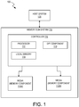
- FIG. 1 illustrates an example computing environment that includes a memory sub-system in accordance with some embodiments of the present disclosure.
- FIG. 2 is a flow diagram of an example method to provide data-structure based dynamic program targeting control in accordance with some embodiments of the present disclosure.
- FIGS. 3A and 3B illustrate error count distributions, in accordance with some embodiments of the present disclosure.
- FIGS. 4A-4D illustrate a shifting or program distributions, in accordance with some embodiments of the present disclosure.
- FIG. 5 is a block diagram of an example computer system in which embodiments of the present disclosure may operate.
- a memory sub-system is also hereinafter referred to as a “memory device.”
- An example of a memory sub-system is a storage system, such as a solid-state drive (SSD).
- the memory sub-system is a hybrid memory/storage sub-system.
- a host system can utilize a memory sub-system that includes one or more memory components. The host system can provide data to be stored at the memory sub-system using write (also hereinafter referred to as “program”) requests and can retrieve data from the memory sub-system using read requests.
- write also hereinafter referred to as “program”
- the memory sub-system can include multiple memory components that can store data from the host system.
- Each memory component can include a different type of media. Examples of media include, but are not limited to, a cross-point array of non-volatile memory and flash based memory such as single-level cell (SLC) memory, triple-level cell (TLC) memory, and quad-level cell (QLC) memory.
- SLC single-level cell
- TLC triple-level cell
- QLC quad-level cell
- Memory components such as flash based memory, utilize electrical energy, along with corresponding threshold levels or processing voltage levels, to store and access data.
- electrical characteristics of the memory components i.e. charge retention capabilities
- the electrical characteristics of the memory components can change due to changes in operating temperature of the memory component, which can occur because of, for example, ambient temperature changes and/or heat generated by the memory component during operation.
- the changes in the electrical characteristics can lead to a shift in the threshold voltage distributions (also hereinafter referred to as “program distributions”) in the flash-based memory, which can adversely affect memory operations, such as, for example, read operations, write operations, and/or erase operations.
- PV operations write operations are also hereinafter referred to as “program verify (PV) operations.” If the changes in the electrical characteristics are not properly compensated, the shift in the program distributions can cause performance and reliability issues by, for example, increasing the error count and/or the error rate of memory operations.
- a conventional memory sub-system can have memory components with calibration circuits to provide voltage adjustments (also hereinafter referred to as “trims”) for compensating the gate voltage levels at the memory cells during memory operations to account for a shift in the program distributions (and any associated performance/reliability issues).
- the calibration procedure can include applying the trims to the appropriate gate voltage level when performing read operations and PV operations to minimize errors associated with the memory operations. While these read calibration operations can provide calibrated read levels that reduce the errors, the error count and/or error rate may still not be optimal and the memory sub-system can still experience performance issues.
- PV target levels program-verify target levels
- the firmware can be media-type dependent, which can mean that separate firmware is needed for calibration operations on SLC memory, TLC memory, QLC memory, and other higher-density memories. Accordingly, there is limited flexibility in adjusting the PV target level in conventional memory sub-systems, which can lead to poor performance and/or reliability in the memory sub-system due to, for example, high error counts and/or high error rates during memory operations.
- a memory sub-system can include a DPT component that provides trims to control the shifting of program distributions, including the magnitude, direction, and/or rate of the shifting, based on information in a data-structure.
- the data-structure based DPT component can be media-type independent such that the same DPT component firmware can be used for SLC memory, TLC memory, and QLC memory.
- FIG. 1 illustrates an example computing environment 100 that includes a memory sub-system 110 in accordance with some embodiments of the present disclosure.
- the memory sub-system 110 can include media, such as memory components 112 A to 112 N.
- the memory components 112 A to 112 N can be volatile memory components, non-volatile memory components, or a combination of such.
- the memory sub-system is a storage system.
- An example of a storage system is a SSD.
- the memory sub-system 110 is a hybrid memory/storage sub-system.
- the computing environment 100 can include a host system 120 that uses the memory sub-system 110 .
- the host system 120 can write data to the memory sub-system 110 and read data from the memory sub-system 110 .
- the host system 120 can be a computing device such as a desktop computer, laptop computer, network server, mobile device, or such computing device that includes a memory and a processing device.
- the host system 120 can include or be coupled to the memory system 110 so that the host system 120 can read data from or write data to the memory system 110 .
- the host system 120 can be coupled to the memory system 110 via a physical host interface.
- “coupled to” generally refers to a connection between components, which can be an indirect communicative connection or direct communicative connection (e.g., without intervening components), whether wired or wireless, including connections such as, electrical, optical, magnetic, etc.
- Examples of a physical host interface include, but are not limited to, a serial advanced technology attachment (SATA) interface, a peripheral component interconnect express (PCIe) interface, universal serial bus (USB) interface, Fiber Channel, Serial Attached SCSI (SAS), etc.
- the physical host interface can be used to transmit data between the host system 120 and the memory system 110 .
- the host system 120 can further utilize an NVM Express (NVMe) interface to access the memory devices 112 A to 112 N when the memory system 110 is coupled with the host system 120 by the PCIe interface.
- NVMe NVM Express
- the physical host interface can provide an interface for passing control, address, data, and other signals between the memory system 110 and the host system 120 .
- the memory components 112 A to 112 N can include any combination of the different types of non-volatile memory devices and/or volatile memory devices.
- An example of non-volatile memory devices includes a negative-and (NAND) type flash memory.
- Each of the memory devices 112 A to 112 N can include one or more arrays of memory cells such as single level cells (SLCs), multi-level cells (MLCs) (e.g., triple level cells (TLCs), or quad-level cells (QLCs)).
- a particular memory component can include both an SLC memory portion and a MLC memory portion.
- Each of the memory cells can store one or more bits of data (e.g., data blocks) used by the host system 120 .
- the memory components 112 A to 112 N can be based on any other type of memory such as a volatile memory.
- the memory components 112 A to 112 N can be, but are not limited to, random access memory (RAM), read-only memory (ROM), dynamic random access memory (DRAM), synchronous dynamic random access memory (SDRAM), phase change memory (PCM), magneto random access memory (MRAM), negative-or (NOR) flash memory, electrically erasable programmable read-only memory (EEPROM), and a cross-point array of non-volatile memory cells.
- a cross-point array of non-volatile memory can perform bit storage based on a change of bulk resistance, in conjunction with a stackable cross-gridded data access array. Additionally, in contrast to many flash-based memories, cross point non-volatile memory can perform a write in-place operation, where a non-volatile memory cell can be programmed without the non-volatile memory cell being previously erased. Furthermore, the memory cells of the memory devices 112 A to 112 N can be grouped as memory pages or data blocks that can refer to a unit of the memory device used to store data.
- the memory system controller 115 can communicate with the memory devices 112 A to 112 N to perform operations such as reading data, writing data, or erasing data at the memory devices 112 A to 112 N and other such operations.
- the controller 115 can include hardware such as one or more integrated circuits and/or discrete components, a buffer memory, or a combination thereof.
- the controller 115 can be a microcontroller, special purpose logic circuitry (e.g., a field programmable gate array (FPGA), an application specific integrated circuit (ASIC), etc.), or other suitable processor.
- the controller 115 can include a processor (processing device) 130 configured to execute instructions stored in local memory 122 .
- the local memory 122 of the controller 115 includes an embedded memory configured to store instructions for performing various processes, operations, logic flows, and routines that control operation of the memory sub-system 110 , including handling communications between the memory sub-system 110 and the host system 120 .
- the local memory 122 can include memory registers storing memory pointers, fetched data, etc.
- the local memory 122 can also include read-only memory (ROM) for storing micro-code. While the example memory sub-system 110 in FIG.
- a memory sub-system 110 may not include a controller 115 , and can instead rely upon external control (e.g., provided by an external host, or by a processor or controller separate from the memory sub-system).
- external control e.g., provided by an external host, or by a processor or controller separate from the memory sub-system.
- the controller 115 can receive commands or operations from the host system 120 and can convert the commands or operations into instructions or appropriate commands to achieve the desired access to the memory components 112 A to 112 N.
- the controller 115 can be responsible for other operations such as wear leveling operations, garbage collection operations, error detection and error-correcting code (ECC) operations, encryption operations, caching operations, and address translations between a logical block address and a physical block address that are associated with the memory components 112 A to 112 N.
- the controller 115 can further include host interface circuitry to communicate with the host system 120 via the physical host interface.
- the host interface circuitry can convert the commands received from the host system into command instructions to access the memory components 112 A to 112 N as well as convert responses associated with the memory components 112 A to 112 N into information for the host system 120 .
- the memory sub-system 110 can also include additional circuitry or components that are not illustrated.
- the memory sub-system 110 can include a cache or buffer (e.g., DRAM) and address circuitry (e.g., a row decoder and a column decoder) that can receive an address from the controller 115 and decode the address to access the memory components 112 A to 112 N.
- Each of the memory components 112 A to 112 N can include one or more dies.
- the memory sub-system 110 includes a DPT component 113 that can operably interface to a data-structure (or data-structures) to adjust characteristics of memory cells based on memory operations.
- the DPT component 113 can operably interface to a data-structure (or data-structures) that contains information related to, for example, changing a magnitude, a direction, and/or a rate of a characteristic of one or more memory cells.
- the characteristic of the memory cells can be, for example, a threshold voltage level corresponding to a read operation, a PV operation, and/or an erase operation for the memory cells.
- the memory cells can correspond to, for example, a page type, a logical or stored value, a word line group (WLG), a word line, a memory component, or any combination thereof.
- the controller 115 includes at least a portion of the DPT component 113 .
- the controller 115 can include a processor 117 (processing device) configured to execute instructions stored in local memory 119 for performing the operations described herein.
- the DPT component 113 is part of the host system 110 , an application, or an operating system.
- the DPT component 113 can receive data related to memory operations on memory cells in memory components 112 A to 112 N and change the characteristics of the memory cells based on the received data. For example, in some embodiments, the DPT component 113 can receive an error measure relating to memory operations for a group of memory cells. The error measure can be received from, for example, operations executed on the memory sub-system 110 and/or the host system 120 that measure a success and/or a failure of memory operations (e.g., read, write, and/or erase operations). In some embodiments, the error measure can be calculated by the DPT component 113 .
- the error measure can represent a degree, a frequency, an amount or magnitude, a size or number, a processing derivation of errors, or a combination thereof describing errors related to the memory operations.
- the error measure can include an error count, an error rate, or a combination thereof.
- the error count can represent an amount or magnitude, a degree, a size or number, or a combination thereof describing the errors.
- the error count can be a bit error count (BEC).
- BEC bit error count
- the error rate can represent a frequency or a probability of occurrence of the errors, a proportional amount or a percentage of errors, or a combination thereof.
- the error rate can include a bit error rate (BER).
- the error measure can correspond to one or more units or groupings within the memory cells of the memory component.
- the error measure can be for one or more of memory pages, word-line groups, memory components, or any combination thereof corresponding to the memory cells.
- the error measure can correspond to the page type, such as for the lower page (LP), the upper page (UP), the extra page (XP), or the top page (TP).
- the error measure can be calculated or tracked by operations executed in the host device 120 , the controller 115 , or a combination thereof.
- the error measure can be stored in the host device 120 , local memory 119 , one or more of memory components 112 A to 112 N, another memory location of the memory sub-system 110 , or any combination thereof.
- the DPT component 113 receives feedback information related to errors (e.g., an error measure) during memory operations.
- the feedback information can include an error count and/or an error rate corresponding to read operations on one or more memory cells.
- the feedback information can be received from, for example, operations executed on the memory sub-system 110 and/or the host system 120 that measure a success and/or a failure of memory operations (e.g., read, write, and/or erase operations).
- the feedback information can be calculated by the DPT component 113 .
- the DPT component 113 changes threshold voltage characteristics of the memory cells to adjust an error measure between a group of memory cells in accordance with information stored in a data-structure, such as, for example, a look-up-table (LUT).
- the adjustment can include equalizing (also referred to herein as “balancing”) the error measure between a group of memory cells in accordance with information stored in a data-structure, such as, for example, a LUT.
- equalizing also referred to herein as “balancing”
- balancing the error measure between a group of memory cells in accordance with information stored in a data-structure, such as, for example, a LUT.
- equalize and “balance” mean that the values being compared are within a predetermined deadband and/or an operation involving adjustments to a program distribution enters a dither condition.
- the data-structure can be located in local memory 119 , in one or more of memory components 112 A to 112 N, in some other memory in memory sub-system 110 , in the host system 120 , or in any combination thereof.
- the data-structure can be in volatile or non-volatile memory.
- the changing of the characteristics of the memory cells in memory components 112 A to 112 N can include shifting the program distributions for a group of memory cells to equalize an error measure (e.g., BEC, BER, etc.) between the group of memory cells.
- the DPT component 113 can operably be coupled to a data-structure (e.g., LUT) that holds information for shifting one or more of the program distributions.
- the data-structure can include information relating to a trim for a PV target level that shifts the corresponding program distribution in subsequent PV operations to equalize the error measure.
- the trim information (hereinafter also referred to as “PV target level trim information”) can include information related to the magnitude and direction of the shift change and/or a rate of change (also referred to herein as “bandwidth”) of the shift of the program distributions.
- the information can be, for example, a voltage value representing the amount and/or direction to shift the program distribution and can be given in, for example, millivolts (mV) and/or ticks.
- a tick can correspond to a minimum threshold voltage adjustment of the memory sub-system 110 (e.g., due to the granularity of an analog-to-digital converter (ADC)).
- ADC analog-to-digital converter
- the program distributions can be shifted when the memory sub-system 110 performs subsequent PV operations using the new PV target levels.
- the DPT component 113 can include pointers that identify the location where the data-structure is stored in memory.
- the data-structure can be stored in, for example, local memory 119 , one or more of memory components 112 A to 112 N, memory in host system 120 , other memory in memory sub-system 110 , or any combination thereof.
- the DPT component 113 can use the PV target level trim information to adjust (e.g., equalize) the error measure between page types (e.g., LP, UP, and XP page-types in TLC type memory cells) and/or adjust (e.g., equalize) the read window budget (RWB) by valley within each page type.
- the RWB relates to a separation between a read level voltage used in read operations and voltages corresponding to adjacent logic states. Further details with regards to the operations of the characteristic component 113 are described below.
- FIG. 2 is a flow diagram of an example method 200 to shift a program distribution based on information stored in a data-structure, in accordance with some embodiments of the present disclosure.
- the method 200 can be performed by processing logic that can include hardware (e.g., processing device, circuitry, dedicated logic, programmable logic, microcode, hardware of a device, integrated circuit, etc.), software (e.g., instructions run or executed on a processing device), or a combination thereof.
- the method 200 is performed by the DPT component 113 of FIG. 1 . Although shown in a particular sequence or order, unless otherwise specified, the order of the processes can be modified.
- the processing device receives feedback related to errors in memory operations on one or more memory cells.
- the feedback can be an error measure (e.g., a BER, a BEC, etc.) that is related to one or more program distributions.
- the feedback relates to a center error count and/or a differential error count.
- the memory operations can be, for example, read, program, and/or erase operations.
- the feedback can relate to an error count associated with read operations.
- the feedback can be received from, for example, operations executed on the memory sub-system 110 and/or the host system 120 that measure a success and/or a failure of memory operations (e.g., read, write, and/or erase operations).
- the information used in the feedback can be calculated by the DPT component 113 .
- the memory cells can correspond to memory cells of a same page type, such as, for example, a LP level page, a UP level pages, a XP level page, a TP level page, etc., depending on the type of memory cells.
- the processing device updates, based on the feedback and information stored in the data-structure, at least one processing level corresponding to a program distribution to adjust an error measure between pages of the memory cells and to adjust a read window budget within a page of the memory cells.
- the adjusting of the error measure equalizes the error measure between pages of the plurality of memory cells.
- the adjusting of the read window budget equalizes read window budgets within the page.
- Processing level means the threshold voltage used for performing a memory operation (e.g., a read operation, a PV operation, or an erase operation) on a memory cell.
- the processing level is the respective threshold voltage corresponding to level L0 to level L7 for a given type of memory operation.
- the processing level corresponds to the target voltage levels used for verifying that the memory cell is at the charge level corresponding to a desired program distribution (e.g. level L0 to level L7 in a TLC-type memory).
- Updating the processing level can include changing (e.g., shifting) the threshold voltage level values corresponding the program distribution based on an error measure of a memory operation (e.g., a read memory operation).
- updating the processing levels can include comparing the error measure (e.g., BER, BEC, etc.) between pages of memory cells.
- the error measure on of the LP page can be respectively compared to the error measures of the other pages (e.g., LP to UP, LP to XP, LP to TP, etc.).
- the program distribution level on the other page determines how the processing levels are to be shifted (if at all) in order to adjust (e.g., to equalize) the RWB within a page and/or the error measure between page types.
- the program distribution level on the other page having the smallest RWB determines how the processing levels are to be shifted (if at all) in order to adjust (e.g., to equalize) the RWB within a page and/or the error measure between page types. Exemplary embodiments that update processing levels are described in more detail below.
- the updating can be based on trim information for the at least one processing level that is stored in a data-structure.
- the data-structure can be a LUT and can include trim information for adjusting a target level such as, for example, a PV target level.
- the PV target level trim information can include, for example, information related to a magnitude and a bandwidth of the desired shift in the program distributions in, for example, mVs or ticks. Further details with regards to the method of operation of the memory sub-system 110 , including DPT component 113 , are described below.
- the memory sub-system 110 can track an error measure for the memory operations.
- the error measure can include a BEC, a BER, etc.
- the error measure can correspond to one or more units or groupings within the memory cells of the memory components 112 A to 112 N.
- the error measure can be for one or more memory pages, word-line groups, memory components, or any combination thereof corresponding to the memory cells.
- the error measure can correspond to the page type (e.g., LP, UP, XP, TP, etc. depending on the memory type).
- the error measure can be calculated or tracked by the host device 120 , the controller 115 , or a combination thereof.
- FIGS. 3A and 3B illustrate example error count distributions 310 , 350 , respectively, that can be used by the DPT component 113 (or another operation) to generate feedback information to be used by the DPT component for adjusting (e.g., equalizing) an error measure (e.g., BEC, BER, etc.) between memory pages and/or the RWB within a memory page during memory operations in the memory sub-system 110 .
- the error count distributions 310 , 350 in FIGS. 3A and 3B can represent error counts of program distributions within a same page in the memory cells (e.g., UP, XP, TP, etc. based on the memory type).
- the y-axis of the error count distributions 310 , 350 represents the error count (e.g., a BER, BEC, etc.) of the memory operation on memory cells corresponding to a respective program distribution, and the x-axis represents the threshold voltage levels Vt used in the memory operation for the respective program distribution.
- FIG. 3A can represent an error count distribution corresponding to a program distribution having a wide valley
- FIG. 3B can represent an error count distribution corresponding to a narrow valley. Because its distribution valley is wide, error count distribution 310 has a larger RWB relative to the RWB of error count distribution 350 .
- the error count distributions 310 , 350 can be the error counts corresponding to read operations.
- the error count distributions 310 , 350 can be created by operations, e.g., read calibration operations, executed by the host device 120 , the controller 115 , or a combination thereof.
- the error count distributions 310 , 350 can be based on error count data corresponding to multiple memory operations on a group of memory cells.
- information from read operations can be used to generate the error count distributions 310 , 350 .
- a memory page in the group of memory cells can be randomly selected, and using a read level voltage corresponding to a program distribution level for the memory page, the selected memory page can be sampled and an error count determined. After multiple memory operations, the error count distributions 310 , 350 can be generated.
- the error count distributions 310 , 350 can be based on the component, the page type (e.g., LP, UP, and/or XP for a TLC type memory cells), the WLG, the level (e.g., L0 to L7 for TLC type memory cells), or any combination thereof.
- the error count distributions 310 , 350 can be based on each page-type for each WLG.
- the error count distributions 310 , 350 can correspond to read operation error data for two separate logic levels from a same page type (e.g., a UP page or an XP page in TLC memory cells).
- the shape (e.g., width, depth, slope, symmetry, etc.) of each error count distribution 310 , 350 can correlate to the valley shape between adjacent program distributions, which relates to the RWB of the valley.
- the DPT component 113 can sample and/or receive error count readings corresponding to the error count distributions 310 , 350 , including center error count readings 312 and 352 as respectively illustrated in FIGS. 3A and 3B .
- the error count distributions 310 , 350 can be stored in the host device 120 , local memory 119 , one or more of memory components 112 A to 112 N, another memory location of the memory sub-system 110 , or any combination thereof.
- the center error count readings 312 , 352 can correspond to a processing level voltage having the lowest error count.
- the center error count readings 312 , 352 can correspond to a read level voltage (e.g., a read level derived from a read calibration operation) that can be used in read operations for that page.
- the center error count readings 312 , 352 can be used as feedback data that can be used by the DPT component 113 to equalize the error measures (e.g., BEC, BER, etc.) between page types of a group of memory cells (e.g., equalize the error measure between LP, UP, and XP pages of a WLG in TLC memory).
- the error measures e.g., BEC, BER, etc.
- the performance of the memory sub-system 110 can still be less than optimal because the RWB magnitudes of valleys within each page type of the group of memory cells may not be balanced.
- the RWB magnitudes of the valleys within each page type e.g., within UP pages and within XP pages of TLC memory cells
- a valley shape e.g., width, depth, slope, symmetry, etc.
- matching the valley shapes within each page type will also mean balancing the RWB within each page type.
- each set of readings can respectively include a center error count reading 312 , 352 , as discussed above, a first error count reading 314 , 354 , and a second error count reading 316 , 356 .
- the first error count readings 314 , 354 are sampled at processing level voltages that are offset from the respective center processing level voltage by predetermined voltage magnitudes in a negative voltage direction, as shown by first offsets 324 , 364 in FIGS. 3A and 3B , respectively.
- the second error count readings 316 , 356 are sampled at processing level voltages that are offset from the respective center processing level voltage by predetermined voltage magnitudes in a positive voltage direction, as shown by second offsets 326 , 366 , respectively.
- Each of the first offsets 324 , 364 and the second offsets 326 , 366 can have a predetermined magnitude that ranges from, for example, 10 ticks to 50 ticks.
- a tick can correspond to a minimum threshold voltage adjustment of the memory sub-system 110 (e.g., due to the granularity of an analog-to-digital converter (ADC)).
- a tick can be, for example, in a range of 10 mV to 20 mV.
- the first offset is equal in magnitude to the second offset. In other embodiments, the first and second offset magnitudes can be different.
- a differential error count can be calculated by the DPT component 113 (and/or another operation, such as, e.g., a read level calibration operation) based on a difference between the center error count reading and a mean of the first and second error count readings.
- Diff-EC is a measure of the valley shape with a larger Diff-EC value corresponding to a narrower valley shape.
- the RWB magnitudes of valleys in a page type correspond to the shape of the valleys
- equalizing the Diff-EC values within a page type also means that the RWB magnitudes of the respective valleys will be balanced.
- information based on the center error counts 312 , 352 and/or the Diff-ECs for the error count distributions 310 , 350 can be used as feedback information by the DPT component 113 to equalize an error measure (e.g., BEC, BER, etc.) for memory cells during memory operations.
- an error measure e.g., BEC, BER, etc.
- the magnitudes of the first offsets 324 , 364 and/or second offsets 326 , 366 can be adjusted either manually (e.g., by a user) or automatically (e.g., by the DPT component 113 or another operation) to optimize the center error reading and/or the Diff-EC calculation information to the DPT component 113 .
- the DPT component 113 can use small offset magnitudes and still calculate a Diff-EC value that can accurately identify the shape of the valley. However, as the valleys widen (e.g., due to equalizing the error measure), the DPT component 113 may need to use larger offset magnitudes in order for the Diff-EC value to identify the valley shape.
- an averaged center error count reading based on the plurality of center count readings 312 , 352 and an averaged Diff-EC value based on the plurality of Diff-EC values can be used as the feedback information by the DPT component 113 .
- the DPT component 113 can receive the feedback information (e.g., the center error count reading and/or the Diff-EC value) and use the feedback information to shift program distributions (e.g., by changing PV target levels) in order to equalize the error measure (e.g., BEC and/or BER) in the memory cells.
- the error measure e.g., BEC and/or BER
- At least a portion of the information relating to the instructions for shifting the program distribution can be stored in a data-structure (e.g., an LUT) that is operably connected to the DPT component 113 .
- the portion of the instructions stored in the data-structure (e.g., LUT) are hereinafter referred to as “rules” or “program distribution rules.”
- the program distribution shift information is based on the page type (e.g., UP, XP, and/or the TP page, as appropriate based on memory type) and relative to the LP page.
- QLC memory cells can have a set of rules for the LP-UP page set that adjusts the UP page program distributions relative to the LP page, a set of rules for the LP-XP page set that adjusts the XP page program distributions relative to the LP page, and a set of rules for the LP-TP page set that adjusts the TP page program distributions relative to the LP page.
- a single data-structure e.g., LUT
- the data-structures can be configured such that each data-structure (e.g., LUT) stores the program distribution rules for a single page set (e.g., an LP-UP page set, an LP-XP page set, or an LP-TP page set as appropriate depending on memory type).
- the memory sub-system 110 (or host system 120 ) can store multiple data-structures (e.g., LUTs) with each data-structure storing the program distribution rules for a page type, a memory type, or a combination thereof.
- the rules accessed by the DPT component 113 include at least information on the magnitude and direction for shifting each program distribution and/or bandwidth for each program distribution shift.
- the DPT component 113 can perform continuous, period, and/or on-demand calibrations to balance the error measure (e.g., BEC. BER, etc.) between the pages (e.g., LP, UP, XP, and TP depending on the memory type) of the memory cells and/or balance the RWB magnitudes of valleys within each page.
- error measure e.g., BEC. BER, etc.
- pages e.g., LP, UP, XP, and TP depending on the memory type
- the data-structure based DPT component of the present disclosure allows for the DPT component firmware code to be reduced because a small collection of code routines can be used with multiple memory types (e.g., SLC, MLC, TLC, QLC, etc.) by just interchanging the data-structures and/or changing the pointers to data-structures to select the desired data-structures.
- the data-structure based DPT component is robust and requires less memory resources than hard coding all the rules.
- the rules can be changed as desired without recoding the firmware algorithm and/or having to perform extensive code testing on the firmware.
- the data-structure of the present disclosure also provides greater flexibility than a hard-coded algorithm.
- the data-structures and/or associated rules can be added, edited, and/or deleted either manually by a user (static control) and/or automatically by the memory sub-system 110 and/or the host 120 (dynamic control).
- the memory sub-system 110 can use dynamic state space observer control based on, for example, disturbs, retention, and/or program/erase cycling limits, to add, edit, and/or delete data-structures and/or the associated rules detailing the magnitude and direction for shifting the program distributions and/or bandwidth for the program distributions as desired to optimize performance of the memory sub-system 110 .
- multiple sets of data-structures having multiple sets of rules can be used throughout the lifetime of the memory sub-system 110 .
- the appropriate data-structure or data-structures can be modified and/or switched.
- the data-structures can be modified or switched based on the usage and/or remaining life of the memory sub-system 110 .
- a first set of data-structures with a first set of program distribution rules can be used when the memory sub-system 110 is new, a second set of data-structures with a second set of program distribution rules can be used during mid-life of the memory sub-system 110 , and a third set of data-structures with a third set of program distribution rules can be used at the end-of-life of the memory sub-system 110 .
- An example set of rules for shifting the program distributions for an LP-UP page set and an LP-XP page set in a TLC memory type is described with reference to Table 1.
- the information in at least columns L1 to L7 can be incorporated to a data-structure as rules to provide instructions to the DPT component 113 on how to shift the appropriate program distribution.
- the data in columns L1 to L7 of Table 1 provides the magnitude and direction the PV target levels (and thus the program distributions) should be shifted based on error distributions of memory operations (see, e.g., error distributions 310 , 350 ).
- a “+1” value for a program distribution means that the PV target level (or threshold target voltage) for that program distribution L1 to L7 should be shifted by 1 tick in the positive voltage direction.
- a “ ⁇ 1” for a program distribution means that the PV target level should shifted in the negative voltage direction by 1 tick.
- a tick is the minimum voltage adjustment that the memory sub-system 110 can provide and can be a value in a range of 10 mV to 20 mV.
- a “0” in columns L1 to L7 means that no adjustment is made and that program distribution is fixed.
- the DPT component 113 receives the center error count from the target levels corresponding to memory operations such as, for example, read levels when performing read operations, as discussed above with respect to FIGS. 3A and 3B . Based on the center error count for a given target level, the DPT component 113 updates the LP-UP page set by determining which page between LP and UP has the higher BER. For clarity, BER is used in the description but other error criteria that relate to the error measure of the memory operation can be used. Case nos. 1 and 2 of Table 1 are followed when the UP page has a higher BER than the LP page. The DPT component 113 then determines which case no. (1 or 2) to apply by checking which UP valley has the higher Diff-EC value.
- a larger Diff-EC value equates to a valley shape that is narrower, which corresponds to a smaller RWB magnitude.
- the DPT component 113 attempts to equalize the RWB magnitude between valleys of the same page by broadening the valley having the largest Diff-EC (smaller RWB). Accordingly, to equalize the RWB between valleys V2 and V6 of the UP page, the DPT component 113 will select case no. 1 if V2 has the largest Diff-EC and case no. 2 if V6 has the largest Diff-EC. If case no.
- the target levels (which can be, e.g., PV target levels) for the L2 and L3 program distributions are shifted by 1 tick in the positive voltage direction. If case no. 2 is selected by the DPT component 113 , then the target levels for the L4 and L5 program distributions are shifted by 1 tick in the negative voltage direction. If the LP page has a higher BER than the UP page, the DPT component 113 can execute similar instructions but instead of selecting a UP valley with the higher Diff-EC, the DPT component 113 selects a UP valley with the smallest Diff-EC in order to narrow the UP valley so that the LP valley V4 can be broadened.
- the DPT component 113 selects a UP valley with the smallest Diff-EC in order to narrow the UP valley so that the LP valley V4 can be broadened.
- the instructions for shifting the program distributions for the LP-XP page set are similar to those given above for the LP-UP page set. However, for the XP page, there are three XP valleys that must be checked for the RWB magnitude. In some embodiments such as that shown in Table 1, the XP valley V1 is not used in the RWB checks and the XP valley V1 is also not adjusted. However, in some embodiments, the XP valley V1 can be used and/or adjusted. Similarly, although program distributions L0, L1, and/or L0 are fixed (not shifted) in some embodiments (such as the embodiment of Table 1), in other embodiments, one or more of the program distributions L0, L1, and L7 can be shifted.
- the LP-UP update can be performed in the same operation cycle (e.g., a program/erase cycle) as the LP-XP update. In other embodiments, the LP-UP update and the LP-XP update are performed in different operation cycles. In some embodiments, the LP-UP and LP-XP updates are performed in alternate operation cycles (e.g., in alternate program/erase cycles). In the above disclosure, although a single LP-UP and LP-XP update cycle was discussed, in some embodiments, multiple update cycles may be performed via iteration before the BER is equalized between page types (e.g., page types within a WLG) and/or the RWB magnitudes are equalized within the same page type.
- the rules for shifting the program distributions can have symmetry.
- the rules for shifting the program distributions case nos. 3 and 4 are the same as the rules for case nos. 1 and 2 but have an opposite polarity.
- Case nos. 5-7 and case nos. 8-10 for the LP-XP update have a similar opposite-polarity symmetry. Due to this symmetry, the instructions for cases nos. 3 and 4 (or 1 and 2) and the instructions for case nos. 8-10 (or 5-7) do not have to be included in the data-structure, which can save memory resources in the memory sub-system 110 .
- the data-structure e.g., LUT
- the DPT component 113 can be configured to change the polarity (direction) of the target level shift as appropriate depending on the case no.
- each program distribution (e.g., L1 to L7) can be shifted independently of the others by providing the magnitude and direction in ticks (or some other voltage measure) in the appropriate location in the data-structure.
- the bandwidth (rate) of the shift. when non-zero is the same for all the program distributions, which is 1 tick.
- the bandwidth can also be set independently for each program distribution and can also include sub-tick increments.
- the bandwidths for program distributions L2 and L3 in case no. 1 are 1.1 ticks, which means that the bandwidth (or rate) is faster (10% faster) than a program distribution having a 1 tick bandwidth.
- the extra 0.1 tick is not immediately applied to the target level of the memory operation (e.g., PV operations) because the memory sub-system 110 can only increment or decrement target levels by a minimum of 1 tick.
- the target levels for L2 and L3 memory operations are only shifted by 1 tick.
- the target levels for L2 and L3 are shifted by 2 ticks.
- the shift for program distribution L3 for case 5 is 0.5 ticks. This means that two update cycles for case 5 are needed before the target voltage level for L3 is shifted by 1 tick (assuming there are no increments or decrements to the L3 sub-tick count based on case no. 8 or another case no.).
- the DPT component 113 (or another operation) can keep track of sub-tick increments and decrements for each program distribution in memory (e.g., local memory 119 , other memory in sub-system 110 , one or more memory components 112 A to 112 N, or any combination thereof) until a full tick for that program distribution is accumulated.
- FIG. 4A illustrates an example of a program distribution profile 402 having program distributions 404 that correspond to logic levels L0 to L7 in TLC type memory cells.
- the program distribution profile 402 can be a calibrated profile that is the result of, for example, a read level calibration and/or a PV target level calibration performed on one or more of the memory components 112 A to 112 N such that the BER between page types LP, UP, and XP and the RWB magnitude of valleys V1 to V7 have been optimized.
- one or more of the program distributions can shift so that an error measure for the appropriate target level (e.g., read levels R1 to R7) during memory operations (e.g., a read operation) causes performance and/or reliability problems.
- the program distributions for L2 and L3 have moved to the left relative to FIG. 4A so that at least valleys V2 and V3 have narrowed and valley V4 has widened.
- the shift in program distributions L2 and L3 can mean that the read levels R2 and R3 might experience higher error counts.
- the RWB magnitudes of UP page valleys V2 and V6 are no longer balanced and the RWB magnitudes of XP valleys V3, V5, and V7 are no longer balanced.
- the program distribution L0 and XP valley V1 which relate to the erased state, are not monitored and are also not adjusted based on the error measure. That is, in some embodiments, only the program distributions L1 to L7 can be adjusted for BER and only valleys V2 to V7 may be adjusted for RWB.
- the DPT component 113 must balance the BER between the LP and UP pages and the BER between LP and XP pages while balancing the RWB magnitudes between the valleys V2 to V7.
- the program distributions L1 to L7 can be adjusted, as discussed below.
- the program distributions L1 and L7 are fixed for better reliability of the memory sub-system 110 and only program distributions L2 to L6 can be adjusted. However, in other embodiments, one or both of L1 and L7 can be adjusted.
- the DPT component 113 determines which page has the worst BER (e.g., compare the center error count of R4 (LP page) to the worst center error count of R2 or R6 (UP page)). If the BERs for the LP and UP pages are already equalized, e.g., within a predetermined value of each other, no PV target level shift is performed.
- the shifting of program distributions L2 and L3 e.g., compare program of FIG. 4A to FIG.
- the DPT component 113 checks to see which UP valley has the larger Diff-EC value.
- the UP valley V2 is narrower than UP valley V6 and thus will likely have the larger Diff-EC value.
- the DPT component 113 will follow case no. 1, which means that the PV target levels for program distributions L2 and L3 will be shifted in the positive voltage direction by 1 tick.
- the +1 tick shift program distributions L2 and L3 is shown in FIG. 4C .
- the DPT component 113 can perform an update on the LP-XP page set in, for example, the next operation cycle (e.g., a program/erase cycle). Similar to the LP-UP update, to equalize the BER between the LP and XP pages (e.g., between the LP and XP pages in each WLG), the DPT component 113 determines which page has the worst BER (e.g., compare the center error count of R4 (LP page) to the worst center error count of R3, R5, or R7 (XP page)). The center error count for R1 is not used and the valley V1 is not adjusted in this embodiment.
- the worst BER e.g., compare the center error count of R4 (LP page) to the worst center error count of R3, R5, or R7 (XP page). The center error count for R1 is not used and the valley V1 is not adjusted in this embodiment.
- the DPT component 113 checks to see which XP valley has the largest Diff-EC value.
- the XP valley V3 is narrower than both V5 and V7 and will likely have the largest Diff-EC value.
- the DPT component 113 will follow case no. 5, which means that the PV target level for program distribution L3 will be shifted in the positive voltage direction by 1 tick.
- the +1 tick shift program distribution L3 is shown in FIG. 4D .
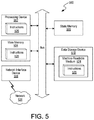
- FIG. 5 illustrates an example machine of a computer system 500 within which a set of instructions, for causing the machine to perform any one or more of the methodologies discussed herein, can be executed.
- the computer system 500 can correspond to a host system (e.g., the host system 120 of FIG. 1 ) that includes, is coupled to, or utilizes a memory sub-system (e.g., the memory sub-system 110 of FIG. 1 ) or can be used to perform the operations of a controller (e.g., to execute an operating system to perform operations corresponding to the DPT component 113 of FIG. 1 ).
- a host system e.g., the host system 120 of FIG. 1
- a memory sub-system e.g., the memory sub-system 110 of FIG. 1
- a controller e.g., to execute an operating system to perform operations corresponding to the DPT component 113 of FIG. 1 .
- the machine can be connected (e.g., networked) to other machines in a LAN, an intranet, an extranet, and/or the Internet.
- the machine can operate in the capacity of a server or a client machine in client-server network environment, as a peer machine in a peer-to-peer (or distributed) network environment, or as a server or a client machine in a cloud computing infrastructure or environment.
- the machine can be a personal computer (PC), a tablet PC, a set-top box (STB), a Personal Digital Assistant (PDA), a cellular telephone, a web appliance, a server, a network router, a switch or bridge, or any machine capable of executing a set of instructions (sequential or otherwise) that specify actions to be taken by that machine.
- PC personal computer
- PDA Personal Digital Assistant
- STB set-top box
- STB set-top box
- a cellular telephone a web appliance
- server a server
- network router a network router
- switch or bridge or any machine capable of executing a set of instructions (sequential or otherwise) that specify actions to be taken by that machine.
- machine shall also be taken to include any collection of machines that individually or jointly execute a set (or multiple sets) of instructions to perform any one or more of the methodologies discussed herein.
- the example computer system 500 includes a processing device 502 , a main memory 504 (e.g., read-only memory (ROM), flash memory, dynamic random access memory (DRAM) such as synchronous DRAM (SDRAM) or Rambus DRAM (RDRAM), etc.), a static memory 506 (e.g., flash memory, static random access memory (SRAM), etc.), and a data storage device 518 , which communicate with each other via a bus 530 .
- main memory 504 e.g., read-only memory (ROM), flash memory, dynamic random access memory (DRAM) such as synchronous DRAM (SDRAM) or Rambus DRAM (RDRAM), etc.
- DRAM dynamic random access memory
- SDRAM synchronous DRAM
- RDRAM Rambus DRAM
- static memory 506 e.g., flash memory, static random access memory (SRAM), etc.
- SRAM static random access memory
- Processing device 502 represents one or more general-purpose processing devices such as a microprocessor, a central processing unit, or the like. More particularly, the processing device can be complex instruction set computing (CISC) microprocessor, reduced instruction set computing (RISC) microprocessor, very long instruction word (VLIW) microprocessor, or processor implementing other instruction sets, or processors implementing a combination of instruction sets. Processing device 502 can also be one or more special-purpose processing devices such as an application specific integrated circuit (ASIC), a field programmable gate array (FPGA), a digital signal processor (DSP), network processor, or the like. The processing device 502 is configured to execute instructions 526 for performing the operations and steps discussed herein.
- the computer system 500 can further include a network interface device 508 to communicate over the network 520 .
- the data storage device 618 can include a machine-readable storage medium 524 (also known as a computer-readable medium) on which is stored one or more sets of instructions or software 526 embodying any one or more of the methodologies or functions described herein.
- the instructions 526 can also reside, completely or at least partially, within the main memory 504 and/or within the processing device 502 during execution thereof by the computer system 500 , the main memory 504 and the processing device 502 also constituting machine-readable storage media.
- the machine-readable storage medium 524 , data storage device 518 , and/or main memory 504 can correspond to the memory sub-system 110 of FIG. 1 .
- the instructions 526 include instructions to implement functionality corresponding to program targeting control (e.g., DPT component 113 of FIG. 1 ).
- the machine-readable storage medium 524 is shown in an example implementation to be a single medium, the term “machine-readable storage medium” should be taken to include a single medium or multiple media that store the one or more sets of instructions.
- the term “machine-readable storage medium” shall also be taken to include any medium that is capable of storing or encoding a set of instructions for execution by the machine and that cause the machine to perform any one or more of the methodologies of the present disclosure.
- the term “machine-readable storage medium” shall accordingly be taken to include, but not be limited to, solid-state memories, optical media and magnetic media.
- the present disclosure also relates to an apparatus for performing the operations herein.
- This apparatus can be specially constructed for the intended purposes, or it can comprise a general purpose computer selectively activated or reconfigured by a computer program stored in the computer.
- a computer program can be stored in a computer readable storage medium, such as, but not limited to, any type of disk including floppy disks, optical disks, CD-ROMs, and magnetic-optical disks, read-only memories (ROMs), random access memories (RAMs), EPROMs, EEPROMs, magnetic or optical cards, or any type of media suitable for storing electronic instructions, each coupled to a computer system bus.
- the present disclosure can be provided as a computer program product, or software, that can include a machine-readable medium having stored thereon instructions, which can be used to program a computer system (or other electronic devices) to perform a process according to the present disclosure.
- a machine-readable medium includes any mechanism for storing information in a form readable by a machine (e.g., a computer).
- a machine-readable (e.g., computer-readable) medium includes a machine (e.g., a computer) readable storage medium such as a read only memory (“ROM”), random access memory (“RAM”), magnetic disk storage media, optical storage media, flash memory devices, etc.
Landscapes
- Engineering & Computer Science (AREA)
- Theoretical Computer Science (AREA)
- Physics & Mathematics (AREA)
- General Engineering & Computer Science (AREA)
- General Physics & Mathematics (AREA)
- Quality & Reliability (AREA)
- Human Computer Interaction (AREA)
- Computer Security & Cryptography (AREA)
- Read Only Memory (AREA)
- Techniques For Improving Reliability Of Storages (AREA)
Abstract
Description
| TABLE 1 | |||||||||||
| BER | |||||||||||
| Center | Case | RWB | |||||||||
| EC | No. | Diff-EC | L1 | L2 | L3 | L4 | L5 | L6 | L7 | ||
| LP-UP | UP > | 1 | V2 Largest | 0 | +1 | +1 | 0 | 0 | 0 | 0 |
| LP | 2 | V6 Largest | 0 | 0 | 0 | −1 | −1 | 0 | 0 | |
| LP > | 3 | V2 Smallest | 0 | −1 | −1 | 0 | 0 | 0 | 0 | |
| UP | 4 | V6 Smallest | 0 | 0 | 0 | +1 | +1 | 0 | 0 | |
| LP-XP | XP > | 5 | V3 Largest | 0 | 0 | +1 | 0 | 0 | 0 | 0 |
| LP | 6 | V5 Largest | 0 | 0 | 0 | −1 | 0 | 0 | 0 | |
| 7 | V7 Largest | 0 | 0 | 0 | −1 | −1 | −1 | 0 | ||
| LP > | 8 | V3 Smallest | 0 | 0 | −1 | 0 | 0 | 0 | 0 | |
| XP | 9 | V5 Smallest | 0 | 0 | 0 | +1 | 0 | 0 | 0 | |
| 10 | V7 Smallest | 0 | 0 | 0 | +1 | +1 | +1 | 0 | ||
| TABLE 2 | |||||||||||
| BER | |||||||||||
| Center | Case | RWB | |||||||||
| EC | No. | Diff-EC | L1 | L2 | L3 | L4 | L5 | L6 | L7 | ||
| LP-UP | LP < | 1 | V2 Largest | 0 | +1.1 | +1.1 | 0 | 0 | 0 | 0 |
| UP | 2 | V6 Largest | 0 | 0 | 0 | −1 | −1 | 0 | 0 | |
| LP > | 3 | V2 Smallest | 0 | −1.1 | −1.1 | 0 | 0 | 0 | 0 | |
| UP | 4 | V6 Smallest | 0 | 0 | 0 | +1 | +1 | 0 | 0 | |
| LP-XP | LP < | 5 | V3 Largest | 0 | 0 | +0.5 | 0 | 0 | 0 | 0 |
| XP | 6 | V5 Largest | 0 | 0 | 0 | −1 | 0 | 0 | 0 | |
| 7 | V7 Largest | 0 | 0 | 0 | −1 | −1 | −1.1 | 0 | ||
| LP > | 8 | V3 Smallest | 0 | 0 | −0.5 | 0 | 0 | 0 | 0 | |
| XP | 9 | V5 Smallest | 0 | 0 | 0 | +1 | 0 | 0 | 0 | |
| 10 | V7 Smallest | 0 | 0 | 0 | +1 | +1 | +1.1 | 0 | ||
Claims (23)
Priority Applications (2)
| Application Number | Priority Date | Filing Date | Title |
|---|---|---|---|
| US16/170,748 US10877832B2 (en) | 2018-10-25 | 2018-10-25 | Data-structure based dynamic program targeting control |
| US17/100,825 US11210154B2 (en) | 2018-10-25 | 2020-11-21 | Data-structure based dynamic program targeting control |
Applications Claiming Priority (1)
| Application Number | Priority Date | Filing Date | Title |
|---|---|---|---|
| US16/170,748 US10877832B2 (en) | 2018-10-25 | 2018-10-25 | Data-structure based dynamic program targeting control |
Related Child Applications (1)
| Application Number | Title | Priority Date | Filing Date |
|---|---|---|---|
| US17/100,825 Continuation US11210154B2 (en) | 2018-10-25 | 2020-11-21 | Data-structure based dynamic program targeting control |
Publications (2)
| Publication Number | Publication Date |
|---|---|
| US20200133754A1 US20200133754A1 (en) | 2020-04-30 |
| US10877832B2 true US10877832B2 (en) | 2020-12-29 |
Family
ID=70326701
Family Applications (2)
| Application Number | Title | Priority Date | Filing Date |
|---|---|---|---|
| US16/170,748 Active 2039-03-12 US10877832B2 (en) | 2018-10-25 | 2018-10-25 | Data-structure based dynamic program targeting control |
| US17/100,825 Active US11210154B2 (en) | 2018-10-25 | 2020-11-21 | Data-structure based dynamic program targeting control |
Family Applications After (1)
| Application Number | Title | Priority Date | Filing Date |
|---|---|---|---|
| US17/100,825 Active US11210154B2 (en) | 2018-10-25 | 2020-11-21 | Data-structure based dynamic program targeting control |
Country Status (1)
| Country | Link |
|---|---|
| US (2) | US10877832B2 (en) |
Families Citing this family (3)
| Publication number | Priority date | Publication date | Assignee | Title |
|---|---|---|---|---|
| US10877832B2 (en) | 2018-10-25 | 2020-12-29 | Micron Technology, Inc. | Data-structure based dynamic program targeting control |
| US11977774B2 (en) | 2021-12-21 | 2024-05-07 | Micron Technology, Inc. | Charge loss mitigation throughout memory device lifecycle by proactive window shift |
| TWI859965B (en) * | 2023-07-11 | 2024-10-21 | 群聯電子股份有限公司 | Memory management method, memory storage device and memory control circuit unit |
Citations (4)
| Publication number | Priority date | Publication date | Assignee | Title |
|---|---|---|---|---|
| US20130227200A1 (en) * | 2012-02-23 | 2013-08-29 | Stec, Inc. | Determining bias information for offsetting operating variations in memory cells based on wordline address |
| US9025374B2 (en) * | 2012-12-13 | 2015-05-05 | Sandisk Technologies Inc. | System and method to update read voltages in a non-volatile memory in response to tracking data |
| US20160148702A1 (en) * | 2014-11-20 | 2016-05-26 | HGST Netherlands B.V. | Calibrating optimal read levels |
| US9431121B2 (en) * | 2014-10-24 | 2016-08-30 | Micron Technology, Inc. | Read voltage adjustment |
Family Cites Families (3)
| Publication number | Priority date | Publication date | Assignee | Title |
|---|---|---|---|---|
| US8661184B2 (en) * | 2010-01-27 | 2014-02-25 | Fusion-Io, Inc. | Managing non-volatile media |
| US10699791B2 (en) * | 2018-08-24 | 2020-06-30 | International Business Machines Corporation | Adaptive read voltage threshold calibration in non-volatile memory |
| US10877832B2 (en) | 2018-10-25 | 2020-12-29 | Micron Technology, Inc. | Data-structure based dynamic program targeting control |
-
2018
- 2018-10-25 US US16/170,748 patent/US10877832B2/en active Active
-
2020
- 2020-11-21 US US17/100,825 patent/US11210154B2/en active Active
Patent Citations (4)
| Publication number | Priority date | Publication date | Assignee | Title |
|---|---|---|---|---|
| US20130227200A1 (en) * | 2012-02-23 | 2013-08-29 | Stec, Inc. | Determining bias information for offsetting operating variations in memory cells based on wordline address |
| US9025374B2 (en) * | 2012-12-13 | 2015-05-05 | Sandisk Technologies Inc. | System and method to update read voltages in a non-volatile memory in response to tracking data |
| US9431121B2 (en) * | 2014-10-24 | 2016-08-30 | Micron Technology, Inc. | Read voltage adjustment |
| US20160148702A1 (en) * | 2014-11-20 | 2016-05-26 | HGST Netherlands B.V. | Calibrating optimal read levels |
Also Published As
| Publication number | Publication date |
|---|---|
| US20200133754A1 (en) | 2020-04-30 |
| US11210154B2 (en) | 2021-12-28 |
| US20210073061A1 (en) | 2021-03-11 |
Similar Documents
| Publication | Publication Date | Title |
|---|---|---|
| US11107543B2 (en) | Adjustment of read and write voltages using a space between threshold voltage distributions | |
| US12169646B2 (en) | Managing threshold voltage drift based on operating characteristics of a memory sub-system | |
| US11651828B2 (en) | First-pass dynamic program targeting (DPT) | |
| US11669380B2 (en) | Dynamic programming of page margins | |
| US11373712B2 (en) | Dynamic programming of valley margins | |
| US10761749B2 (en) | Vectorized processing level calibration in a memory component | |
| US11763914B2 (en) | Adapting an error recovery process in a memory sub-system | |
| US12040026B2 (en) | Adjustment of program verify targets corresponding to a last programming distribution and a programming distribution adjacent to an initial programming distribution | |
| US11210154B2 (en) | Data-structure based dynamic program targeting control | |
| US11914889B2 (en) | Managing an adjustable write-to-read delay based on cycle counts in a memory sub-system | |
| US20230054653A1 (en) | First-pass continuous read level calibration | |
| US11309020B2 (en) | Dragging first pass read level thresholds based on changes in second pass read level thresholds | |
| US11119848B2 (en) | Logic based read sample offset in a memory sub system | |
| US11742053B2 (en) | Managing execution of a scrub operation in view of an operating characteristic of a memory subsystem |
Legal Events
| Date | Code | Title | Description |
|---|---|---|---|
| AS | Assignment |
Owner name: MICRON TECHNOLOGY, INC., IDAHO Free format text: ASSIGNMENT OF ASSIGNORS INTEREST;ASSIGNORS:SHEPEREK, MICHAEL;LIIKANEN, BRUCE A.;KOUDELE, LARRY J.;AND OTHERS;REEL/FRAME:047313/0319 Effective date: 20181019 |
|
| FEPP | Fee payment procedure |
Free format text: ENTITY STATUS SET TO UNDISCOUNTED (ORIGINAL EVENT CODE: BIG.); ENTITY STATUS OF PATENT OWNER: LARGE ENTITY |
|
| AS | Assignment |
Owner name: MORGAN STANLEY SENIOR FUNDING, INC., AS COLLATERAL AGENT, MARYLAND Free format text: SUPPLEMENT NO. 12 TO PATENT SECURITY AGREEMENT;ASSIGNOR:MICRON TECHNOLOGY, INC.;REEL/FRAME:048948/0677 Effective date: 20190416 Owner name: JPMORGAN CHASE BANK, N.A., AS COLLATERAL AGENT, ILLINOIS Free format text: SUPPLEMENT NO. 3 TO PATENT SECURITY AGREEMENT;ASSIGNOR:MICRON TECHNOLOGY, INC.;REEL/FRAME:048951/0902 Effective date: 20190416 |
|
| AS | Assignment |
Owner name: MICRON TECHNOLOGY, INC., IDAHO Free format text: RELEASE BY SECURED PARTY;ASSIGNOR:MORGAN STANLEY SENIOR FUNDING, INC., AS COLLATERAL AGENT;REEL/FRAME:050724/0392 Effective date: 20190731 |
|
| AS | Assignment |
Owner name: MICRON TECHNOLOGY, INC., IDAHO Free format text: RELEASE BY SECURED PARTY;ASSIGNOR:JPMORGAN CHASE BANK, N.A., AS COLLATERAL AGENT;REEL/FRAME:051041/0317 Effective date: 20190731 |
|
| STPP | Information on status: patent application and granting procedure in general |
Free format text: NON FINAL ACTION MAILED |
|
| STPP | Information on status: patent application and granting procedure in general |
Free format text: PUBLICATIONS -- ISSUE FEE PAYMENT RECEIVED |
|
| STCF | Information on status: patent grant |
Free format text: PATENTED CASE |
|
| MAFP | Maintenance fee payment |
Free format text: PAYMENT OF MAINTENANCE FEE, 4TH YEAR, LARGE ENTITY (ORIGINAL EVENT CODE: M1551); ENTITY STATUS OF PATENT OWNER: LARGE ENTITY Year of fee payment: 4 |