US10866448B2 - Array substrate, method for manufacturing the same, display panel and display device - Google Patents
Array substrate, method for manufacturing the same, display panel and display device Download PDFInfo
- Publication number
- US10866448B2 US10866448B2 US16/332,185 US201816332185A US10866448B2 US 10866448 B2 US10866448 B2 US 10866448B2 US 201816332185 A US201816332185 A US 201816332185A US 10866448 B2 US10866448 B2 US 10866448B2
- Authority
- US
- United States
- Prior art keywords
- electrode
- transmitting
- array substrate
- driving electrode
- fingerprint recognition
- Prior art date
- Legal status (The legal status is an assumption and is not a legal conclusion. Google has not performed a legal analysis and makes no representation as to the accuracy of the status listed.)
- Active
Links
Images


Classifications
-
- G—PHYSICS
- G06—COMPUTING OR CALCULATING; COUNTING
- G06V—IMAGE OR VIDEO RECOGNITION OR UNDERSTANDING
- G06V40/00—Recognition of biometric, human-related or animal-related patterns in image or video data
- G06V40/10—Human or animal bodies, e.g. vehicle occupants or pedestrians; Body parts, e.g. hands
- G06V40/12—Fingerprints or palmprints
- G06V40/13—Sensors therefor
- G06V40/1318—Sensors therefor using electro-optical elements or layers, e.g. electroluminescent sensing
-
- G—PHYSICS
- G02—OPTICS
- G02F—OPTICAL DEVICES OR ARRANGEMENTS FOR THE CONTROL OF LIGHT BY MODIFICATION OF THE OPTICAL PROPERTIES OF THE MEDIA OF THE ELEMENTS INVOLVED THEREIN; NON-LINEAR OPTICS; FREQUENCY-CHANGING OF LIGHT; OPTICAL LOGIC ELEMENTS; OPTICAL ANALOGUE/DIGITAL CONVERTERS
- G02F1/00—Devices or arrangements for the control of the intensity, colour, phase, polarisation or direction of light arriving from an independent light source, e.g. switching, gating or modulating; Non-linear optics
- G02F1/01—Devices or arrangements for the control of the intensity, colour, phase, polarisation or direction of light arriving from an independent light source, e.g. switching, gating or modulating; Non-linear optics for the control of the intensity, phase, polarisation or colour
- G02F1/13—Devices or arrangements for the control of the intensity, colour, phase, polarisation or direction of light arriving from an independent light source, e.g. switching, gating or modulating; Non-linear optics for the control of the intensity, phase, polarisation or colour based on liquid crystals, e.g. single liquid crystal display cells
- G02F1/133—Constructional arrangements; Operation of liquid crystal cells; Circuit arrangements
- G02F1/1333—Constructional arrangements; Manufacturing methods
- G02F1/13338—Input devices, e.g. touch panels
-
- G—PHYSICS
- G02—OPTICS
- G02F—OPTICAL DEVICES OR ARRANGEMENTS FOR THE CONTROL OF LIGHT BY MODIFICATION OF THE OPTICAL PROPERTIES OF THE MEDIA OF THE ELEMENTS INVOLVED THEREIN; NON-LINEAR OPTICS; FREQUENCY-CHANGING OF LIGHT; OPTICAL LOGIC ELEMENTS; OPTICAL ANALOGUE/DIGITAL CONVERTERS
- G02F1/00—Devices or arrangements for the control of the intensity, colour, phase, polarisation or direction of light arriving from an independent light source, e.g. switching, gating or modulating; Non-linear optics
- G02F1/01—Devices or arrangements for the control of the intensity, colour, phase, polarisation or direction of light arriving from an independent light source, e.g. switching, gating or modulating; Non-linear optics for the control of the intensity, phase, polarisation or colour
- G02F1/13—Devices or arrangements for the control of the intensity, colour, phase, polarisation or direction of light arriving from an independent light source, e.g. switching, gating or modulating; Non-linear optics for the control of the intensity, phase, polarisation or colour based on liquid crystals, e.g. single liquid crystal display cells
- G02F1/133—Constructional arrangements; Operation of liquid crystal cells; Circuit arrangements
- G02F1/136—Liquid crystal cells structurally associated with a semi-conducting layer or substrate, e.g. cells forming part of an integrated circuit
- G02F1/1362—Active matrix addressed cells
- G02F1/136286—Wiring, e.g. gate line, drain line
-
- G06K9/00013—
-
- G06K9/0002—
-
- G—PHYSICS
- G06—COMPUTING OR CALCULATING; COUNTING
- G06V—IMAGE OR VIDEO RECOGNITION OR UNDERSTANDING
- G06V40/00—Recognition of biometric, human-related or animal-related patterns in image or video data
- G06V40/10—Human or animal bodies, e.g. vehicle occupants or pedestrians; Body parts, e.g. hands
- G06V40/12—Fingerprints or palmprints
- G06V40/13—Sensors therefor
- G06V40/1306—Sensors therefor non-optical, e.g. ultrasonic or capacitive sensing
-
- H01L27/323—
-
- H01L27/3272—
-
- H01L27/3276—
-
- H—ELECTRICITY
- H10—SEMICONDUCTOR DEVICES; ELECTRIC SOLID-STATE DEVICES NOT OTHERWISE PROVIDED FOR
- H10K—ORGANIC ELECTRIC SOLID-STATE DEVICES
- H10K59/00—Integrated devices, or assemblies of multiple devices, comprising at least one organic light-emitting element covered by group H10K50/00
- H10K59/10—OLED displays
- H10K59/12—Active-matrix OLED [AMOLED] displays
- H10K59/126—Shielding, e.g. light-blocking means over the TFTs
-
- H—ELECTRICITY
- H10—SEMICONDUCTOR DEVICES; ELECTRIC SOLID-STATE DEVICES NOT OTHERWISE PROVIDED FOR
- H10K—ORGANIC ELECTRIC SOLID-STATE DEVICES
- H10K59/00—Integrated devices, or assemblies of multiple devices, comprising at least one organic light-emitting element covered by group H10K50/00
- H10K59/40—OLEDs integrated with touch screens
-
- G—PHYSICS
- G02—OPTICS
- G02F—OPTICAL DEVICES OR ARRANGEMENTS FOR THE CONTROL OF LIGHT BY MODIFICATION OF THE OPTICAL PROPERTIES OF THE MEDIA OF THE ELEMENTS INVOLVED THEREIN; NON-LINEAR OPTICS; FREQUENCY-CHANGING OF LIGHT; OPTICAL LOGIC ELEMENTS; OPTICAL ANALOGUE/DIGITAL CONVERTERS
- G02F1/00—Devices or arrangements for the control of the intensity, colour, phase, polarisation or direction of light arriving from an independent light source, e.g. switching, gating or modulating; Non-linear optics
- G02F1/01—Devices or arrangements for the control of the intensity, colour, phase, polarisation or direction of light arriving from an independent light source, e.g. switching, gating or modulating; Non-linear optics for the control of the intensity, phase, polarisation or colour
- G02F1/13—Devices or arrangements for the control of the intensity, colour, phase, polarisation or direction of light arriving from an independent light source, e.g. switching, gating or modulating; Non-linear optics for the control of the intensity, phase, polarisation or colour based on liquid crystals, e.g. single liquid crystal display cells
- G02F1/133—Constructional arrangements; Operation of liquid crystal cells; Circuit arrangements
- G02F1/136—Liquid crystal cells structurally associated with a semi-conducting layer or substrate, e.g. cells forming part of an integrated circuit
- G02F1/1362—Active matrix addressed cells
- G02F1/136218—Shield electrodes
-
- G02F2001/136218—
-
- H01L2227/323—
-
- H01L27/3225—
-
- H—ELECTRICITY
- H10—SEMICONDUCTOR DEVICES; ELECTRIC SOLID-STATE DEVICES NOT OTHERWISE PROVIDED FOR
- H10K—ORGANIC ELECTRIC SOLID-STATE DEVICES
- H10K59/00—Integrated devices, or assemblies of multiple devices, comprising at least one organic light-emitting element covered by group H10K50/00
-
- H—ELECTRICITY
- H10—SEMICONDUCTOR DEVICES; ELECTRIC SOLID-STATE DEVICES NOT OTHERWISE PROVIDED FOR
- H10K—ORGANIC ELECTRIC SOLID-STATE DEVICES
- H10K59/00—Integrated devices, or assemblies of multiple devices, comprising at least one organic light-emitting element covered by group H10K50/00
- H10K59/10—OLED displays
- H10K59/12—Active-matrix OLED [AMOLED] displays
- H10K59/1201—Manufacture or treatment
-
- H—ELECTRICITY
- H10—SEMICONDUCTOR DEVICES; ELECTRIC SOLID-STATE DEVICES NOT OTHERWISE PROVIDED FOR
- H10K—ORGANIC ELECTRIC SOLID-STATE DEVICES
- H10K59/00—Integrated devices, or assemblies of multiple devices, comprising at least one organic light-emitting element covered by group H10K50/00
- H10K59/10—OLED displays
- H10K59/12—Active-matrix OLED [AMOLED] displays
- H10K59/131—Interconnections, e.g. wiring lines or terminals
Definitions
- the present disclosure relates to the field of fingerprint recognition technology, and particularly to an array substrate, a method for manufacturing the same, a display panel, and a display device.
- the fingerprint is the texture formed by the skin of the bulge (ridge) and the depression (valley) on the fingertip of the human finger. It is naturally formed in the evolutionary process of human beings. Because fingerprints have the characteristics of lifetime immutability, uniqueness and convenience, they have become synonymous with biometric identification, and are widely used in the field of identity information authentication and identification such as security and attendance.
- fingerprint recognition in the field of display device (e.g., mobile phone or tablet computer) as an example, it can be used for, for example, identity authentication of a user.
- display device e.g., mobile phone or tablet computer
- fingerprint recognition component and display device has attracted wide attention.
- An aspect of the present disclosure provides an array substrate.
- the array substrate includes: a plurality of data lines, a plurality of gate lines, and a fingerprint recognition region located on a basal substrate;
- the fingerprint recognition region includes: a plurality of transmitting electrodes and a plurality of sensing electrodes intersected with the plurality of transmitting electrodes; each transmitting electrode is electrically connected to one of the plurality of gate lines.
- an extending direction of the plurality of transmitting electrodes is same to an extending direction of the plurality of gate lines, and an extending direction of the plurality of sensing electrodes is perpendicular to the extending direction of the plurality of transmitting electrodes.
- a portion of the gate line located in the fingerprint recognition region constitutes the transmitting electrode; a width of a portion of the gate line located in the fingerprint recognition region is greater than a width of a portion of the gate line located outside the fingerprint recognition region.
- the transmitting electrode and the gate line are in different layers, and/or the sensing electrode and the data line are in different layers.
- the array substrate includes a first driving electrode connected to the data line, and a second driving electrode located opposite to the first driving electrode; the first driving electrode is located between the basal substrate and the second driving electrode; the transmitting electrode and the first driving electrode are located in a same layer, and a material of the transmitting electrode is same to a material of the first driving electrode; and/or the sensing electrode and the second driving electrode are located in a same layer, and a material of the sensing electrode is same to a material of the second driving electrode.
- the array substrate includes a first driving electrode connected to the data line, and a second driving electrode located opposite to the first driving electrode; the second driving electrode is located between the basal substrate and the first driving electrode; the transmitting electrode and the second driving electrode are located in a same layer, and a material of the transmitting electrode is same to a material of the second driving electrode; and/or the sensing electrode and the first driving electrode are located in a same layer, and a material of the sensing electrode is same to a material of the first driving electrode.
- each transmitting electrode is connected to a corresponding gate line through a plurality of via holes.
- the fingerprint recognition region is provided with an alignment mark; and/or the array substrate further includes a bonding region, and the bonding region is provided with an alignment mark.
- the plurality of sensing electrodes are located on a side of the plurality of transmitting electrodes facing away from the basal substrate.
- the array substrate further includes a shielding electrode located on a side of the transmitting electrode close to the basal substrate.
- the array substrate further includes a GOA circuit connected to the plurality of gate lines.
- Another aspect of the present disclosure provides a display panel including the array substrate according to any one of the above-mentioned embodiments.
- Another aspect of the present disclosure provides a display device including the above-mentioned display panel and a fingerprint recognition module connected to the plurality of sensing electrodes.
- the display panel further includes a source driving circuit, and the fingerprint recognition module is integrated in the source driving circuit.
- Another aspect of the present disclosure provides a method for manufacturing an array substrate including a fingerprint recognition region; the method includes: providing a plurality of data lines and a plurality of gate lines on a basal substrate; forming a plurality of transmitting electrodes in the fingerprint recognition region, each transmitting electrode being electrically connected to a gate line; and forming a plurality of sensing electrodes intersected with the plurality of transmitting electrodes in the fingerprint recognition region.
- the plurality of gate lines include a set of gate lines spanning the fingerprint recognition region; the step of forming a plurality of transmitting electrodes in the fingerprint recognition region, each transmitting electrode being electrically connected to a gate line includes: for each gate line spanning the fingerprint recognition region, a width of a portion of the gate line located in the fingerprint recognition region is formed to be greater than a width of a portion of the gate line located outside the fingerprint recognition region.
- the plurality of gate lines include a set of gate lines spanning the fingerprint recognition region; the step of forming a plurality of transmitting electrodes in the fingerprint recognition region, each transmitting electrode being electrically connected to a gate line includes: forming a dielectric layer covering the plurality of gate lines; forming a via hole in the dielectric layer for each gate line spanning the fingerprint recognition region; an orthographic projection of the gate line on the basal substrate covering an orthographic projection of the via hole on the basal substrate; and forming a plurality of transmitting electrodes on the dielectric layer; each transmitting electrode being electrically connected to the gate line through the via hole.
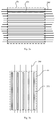
- FIG. 1 is a structural schematic diagram of an array substrate including a fingerprint recognition region according to an embodiment of the present disclosure
- FIG. 2 is a structural schematic diagram of a fingerprint recognition region in an array substrate according to an embodiment of the present disclosure
- FIG. 3 a is structural schematic diagram of a transmitting electrode of a fingerprint recognition region according to an embodiment of the present disclosure
- FIG. 3 b is a structural schematic diagram of a fingerprint recognition region in an array substrate according to an embodiment of the present disclosure
- FIG. 3 c is a structural schematic diagram of a fingerprint recognition region in an array substrate according to another embodiment of the present disclosure.
- FIG. 4 is a schematic cross-sectional view of an array substrate including a fingerprint recognition region according to an embodiment of the present disclosure
- FIG. 5 is a schematic cross-sectional view of an array substrate including a fingerprint recognition region according to another embodiment of the present disclosure
- FIG. 6 is a schematic cross-sectional view of an array substrate including a fingerprint recognition region according to yet another embodiment of the present disclosure
- FIG. 7 is a structural schematic diagram of an array substrate including a fingerprint recognition region according to an embodiment of the present disclosure.
- FIG. 8 is a flowchart of a method for manufacturing an array substrate according to an embodiment of the present disclosure.
- FIG. 9 a is a structural schematic diagram of a mobile phone including a fingerprint recognition region according to an embodiment of the present disclosure.
- FIG. 9 b is a structural schematic diagram of a mobile phone including a fingerprint recognition region according to another embodiment of the present disclosure.
- FIG. 10 is a sequence diagram of an input signal for a gate line according to an embodiment of the present disclosure.
- the present disclosure provides an array substrate, a method for manufacturing the same, a display panel, and a display device.
- the integration degree of the display device including the fingerprint recognition component is improved by integrating the fingerprint recognition component into the array substrate.
- the array substrate includes: a plurality of data lines 200 , a plurality of gate lines 100 , and a fingerprint recognition region 01 located on a basal substrate 10 ;
- the fingerprint recognition region 01 includes: a plurality of transmitting electrodes 101 and a plurality of sensing electrodes 201 intersected with the plurality of transmitting electrodes 101 ; each transmitting electrode 101 is electrically connected to one of the plurality of gate lines 100 .
- the transmitting electrodes and the sensing electrodes in the fingerprint recognition component are both disposed on the array substrate, and the transmitting electrodes are connected to the gate lines.
- the gate driving circuit in the display device can input not only a scanning signal to the gate line but also a transmitting signal to the transmitting electrode through the gate line. Therefore, the integration degree of the display device including the fingerprint recognition component is improved, the procurement of parts is reduced, and the assembly process is simplified.
- the array substrate in the present disclosure may be an array substrate for an LCD (liquid crystal display), or an array substrate for an OLED (organic light emitting diode) display device, which is not limited herein.
- LCD liquid crystal display
- OLED organic light emitting diode
- an extending direction of the plurality of transmitting electrodes 101 is same to an extending direction of the plurality of gate lines 100 , and an extending direction of the plurality of sensing electrodes 201 is perpendicular to the extending direction of the plurality of transmitting electrodes 101 .
- the extending direction of the transmitting electrodes 101 in the present disclosure is not particularly limited.
- the extending direction of the transmitting electrodes 101 may also be inconsistent with the extending direction of the gate line 100 . For example, an angle may be formed between the transmitting electrode 101 and the gate line 100 .
- the transmitting electrode 101 may be linear or curved.
- each transmitting electrode is electrically connected to a gate line, thus the gate driving circuit in the display device can input not only a scanning signal to the gate line but also a transmitting signal to the transmitting electrode through the gate line.
- the specific shape of the transmitting electrode 101 is not limited herein. In order to simplify the manufacturing process and ensure an effective connection of the transmitting electrode to the gate line, optionally, the transmitting electrode 101 extends in the same direction as the gate line 100 .
- the extending direction of the sensing electrode 201 is not particularly limited as long as the sensing electrodes 201 and the transmitting electrodes 101 are disposed to intersect with each other to form a fingerprint sensing unit in an array form (i.e., a grid detection structure).
- the extending direction of the sensing electrode 201 is perpendicular to the extending direction of the transmitting electrode 101 .
- the extending direction of the transmitting electrode 101 is the same as the extending direction of the gate line 100
- the extending direction of the sensing electrode 201 is perpendicular to the extending direction of the transmitting electrode 101 .
- the specific settings of the transmitting electrodes 101 and the sensing electrodes 201 are further described below.
- the transmitting electrode 101 can be directly formed by a portion of the gate line 100 located in the fingerprint recognition region 01 . That is, the transmitting electrode 101 and the gate line 100 are of a unitary structure, which can be produced by one manufacturing process.
- the width of the portion of the gate line 100 located in the fingerprint recognition region 01 is greater than the width of the portion of the gate line 100 located outside the fingerprint recognition region 01 to implement the fingerprint recognition function.
- the transmitting electrode 101 and the gate line 100 are located in different layers, that is, the transmitting electrode 101 and the gate line 100 are two independent portions (e.g. manufactured by two manufacturing processes respectively), which are electrically connected.
- the sensing electrode 201 can be made of the same material and be located in the same layer as the data line 200 , that is, the sensing electrode 201 and the data line 200 are fabricated by one manufacturing process, but the they are not electrically connected.
- the width of the sensing electrode 201 may be greater than the width of the data line 200 .
- the data line 200 has a shape of straight line and passes through the fingerprint recognition region 01 ; as shown in FIG. 3 c , the data line 200 is curved at the fingerprint recognition region 01 , thus the fingerprint recognition region 01 is bypassed; the present disclosure is not limited to this arrangement, and can be designed according to actual needs.
- the sensing electrode 201 may also be located at a different layer from the data line 200 , that is, the sensing electrode 201 and the data line 200 are fabricated by two manufacturing processes.
- the data line 200 may bypass the fingerprint recognition region 01 or may pass through the fingerprint recognition region 01 .
- there may be an overlapping region for the sensing electrode 201 and the data the line 200 i.e., the orthographic projections of the sensing electrode 201 and the data the line 200 on the substrate may have an overlapping portion.
- the data signal loaded on the data line 200 may interfere with the sensing signal on the sensing electrode 201 . Therefore, in practice, it is necessary to turn off (or pull down) the electrical signal on the data line 200 during the fingerprint recognition phase to ensure that the fingerprint recognition component can normally acquire the fingerprint pattern.
- the transmitting electrode 101 and the gate line 100 are located in different layers, and the sensing electrode 201 and the data line 200 are located in different layers.
- the array substrate may have other film layers in addition to the gate lines 100 and the data lines 200 .
- two driving electrodes e.g., a pixel electrode and a common electrode
- the transmitting electrode 101 , the sensing electrode 201 , and other conductive film layers in the array substrate can be fabricated by the same manufacturing process.
- Two alternative arrangements are provided below, but the present disclosure is not limited thereto.
- the array substrate includes a first driving electrode D 1 connected to the data line 200 , and a second driving electrode D 2 located opposite to the first driving electrode D 1 ;
- the first driving electrode D 1 is located between the basal substrate 10 and the second driving electrode D 2 ;
- the transmitting electrode 101 and the first driving electrode D 1 are located in a same layer, and a material of the transmitting electrode 101 is same to a material of the first driving electrode D 1 (i.e., the transmitting electrode 101 and the first driving electrode D 1 are fabricated by the same manufacturing process); and/or the sensing electrode 201 and the second driving electrode D 2 are located in a same layer, and a material of the sensing electrode 201 is same to a material of the second driving electrode D 2 (i.e., the sensing electrode 201 and the second driving electrode D 2 are fabricated by the same manufacturing process).
- the transmitting electrode 101 and the first driving electrode D 1 are located in the same layer, and the material of the transmitting electrode 101 is same to the material of the first driving electrode D 1 . Therefore, in the schematic diagram of FIG. 4 , the first driving electrode D 1 is blocked by the transmitting electrode 101 .
- the driving electrode is a pixel electrode; for an array substrate of an OLED display device, the driving electrode is an anode or a cathode connected to the data line.
- the array substrate may be TN (twist nematic) type, ADS (advanced-super dimensional switching) type, IPS (in plane switch) type, and the like.
- the array substrate includes a first driving electrode connected to the data line, and a second driving electrode located opposite to the first driving electrode; the second driving electrode is located between the basal substrate and the first driving electrode; the transmitting electrode and the second driving electrode are located in a same layer, and a material of the transmitting electrode is same to a material of the second driving electrode (i.e., the transmitting electrode and the second driving electrode are fabricated by the same manufacturing process); and/or the sensing electrode and the first driving electrode are located in a same layer, and a material of the sensing electrode is same to a material of the first driving electrode (i.e., the sensing electrode and the first driving electrode are fabricated by the same manufacturing process).
- the array substrate includes a first driving electrode connected to the data line 200 and a second driving electrode disposed opposite the first driving electrode.
- the array substrate may be of the ADS type, the IPS type (i.e., the first driving electrode and the second driving electrode are arranged in different layers with an interval), or the like.
- the first driving electrode is a pixel electrode
- the second driving electrode is a common electrode.
- the first driving electrode is an anode (or cathode) connected to the data line
- the second driving electrode is a cathode (or anode).
- each of the transmitting electrodes 101 is connected to a corresponding gate line 100 through a plurality of via holes 102 .
- FIG. 4 shows that
- a plurality of via holes 102 are disposed along the extending direction of the gate line 100 , so that the transmitting electrode 101 and the gate line 100 are connected at a plurality of points through the via holes 102 , thereby reducing the contact resistance between the transmitting electrode 101 and the gate lines 100 .
- the transmitting electrode 101 and the sensing electrode 201 can be arranged, for example, in the following ways. As shown in FIG. 4 , the transmitting electrode 101 and the gate line 100 are two portions located in different layers and electrically connected, and the sensing electrode 201 and the data line 200 are two portions located in different layers. As shown in FIG. 4 , the transmitting electrode 101 and the gate line 100 are two portions located in different layers and electrically connected, and the sensing electrode 201 and the data line 200 are two portions located in different layers. As shown in FIG.
- the transmitting electrode 101 and the gate line 100 are in an integrated structure in the same layer, the sensing electrode 201 is in the same layer as the data line 200 , and the material of the sensing electrode 201 is same to the material of the data line 200 (i.e., the sensing electrode 201 and the data line 200 are fabricated by the same manufacturing process).
- the sensing electrode 201 and the data line 200 are two portions located in different layers (i.e., fabricated by two manufacturing processes respectively); the transmitting electrode 101 and the gate line 100 are in an integrated structure in the same layer, and the material of the transmitting electrode 101 is same to the material of the gate line 100 .
- the sensing electrode 201 and the data line 200 may be made of the same material and arranged in the same layer (i.e., the sensing electrode 201 and the data line 200 are fabricated by the same manufacturing process), and the transmitting electrode 101 and the gate line 100 are two portions which are located in different layers and are electrically connected.
- the present disclosure is not limited to this, which can be designed according to the needs of the actual fingerprint recognition component and the type of the array substrate.
- the fingerprint recognition region 01 is provided with an alignment mark 20 .
- the alignment mark 20 is disposed in the bonding region.
- the alignment mark 20 may be disposed in the vicinity of the bonding bump of the fan-out region.
- the traces in the trace region can generally be made of titanium-aluminum-titanium (Ti—Al—Ti) material, and a single layer wiring mode can be applied.
- the plurality of sensing electrodes 201 are located on a side of the plurality of transmitting electrodes 101 facing away from the basal substrate 10 . Since the plurality of sensing electrodes 201 are located on a side of the plurality of transmitting electrodes 101 facing away from the basal substrate 101 , when the user's finger is placed on the top side of the embodiment shown in FIG. 4 , the sensing electrodes 201 can sense the fingerprint pattern well.
- the plurality of sensing electrodes 201 may also be located on a side of the plurality of transmitting electrodes 101 facing the basal substrate 101 (i.e., the plurality of sensing electrodes 201 are located between the plurality of transmitting electrodes 101 and the basal substrate 101 ).
- the plurality of sensing electrodes 201 are located between the plurality of transmitting electrodes 101 and the basal substrate 101 .
- the array substrate further includes a shielding electrode 300 located on a side of the transmitting electrode 101 close to the basal substrate 10 . That is, at least in the fingerprint recognition region 01 , the shielding electrode is disposed on the side of the transmitting electrode 101 close to the basal substrate 10 .
- the shielding electrode 300 may be made of a metal material, and one end of the shielding electrode 300 may be grounded.
- the array substrate in the present disclosure further includes a GOA (gate driver on array) circuit connected to the plurality of gate lines. That is, the gate driving circuit is a GOA circuit.
- the GOA circuit can realize input of a scanning signal to the gate line, and can also input a transmitting signal to the transmitting electrode.
- FIG. 7 is an example in which the GOA circuit is disposed on both ends of the gate lines 100 .
- the present disclosure is not limited to this arrangement, and a single-side GOA circuit for the gate lines 100 may also be employed.
- An embodiment the present disclosure provides a method for manufacturing an array substrate including a fingerprint recognition region. As shown in FIG. 8 , the method includes the following steps.
- Step S 101 providing a plurality of data lines and a plurality of gate lines on a basal substrate.
- Step S 102 forming a plurality of transmitting electrodes in the fingerprint recognition region, each transmitting electrode being electrically connected to a gate line.
- Step S 103 forming a plurality of sensing electrodes intersected with the plurality of transmitting electrodes in the fingerprint recognition region.
- the transmitting electrodes and the sensing electrodes in the fingerprint recognition component are both disposed on the array substrate, and the transmitting electrodes are connected to the gate lines.
- the gate driving circuit in the display device can input not only a scanning signal to the gate line but also a transmitting signal to the transmitting electrode through the gate line. Therefore, the integration degree of the display device including the fingerprint recognition component is improved, the procurement of parts is reduced, and the assembly process is simplified.
- step S 102 will be further described below.
- the plurality of gate lines 100 include a set of gate lines crossing the fingerprint recognition region 01 .
- the step S 102 may specifically include: for each gate line 100 crossing the fingerprint recognition region, forming a portion of the gate line 100 located in the fingerprint recognition region 01 with a width greater than a width of a portion of the gate line 100 located outside the fingerprint recognition region 01 .
- the plurality of gate lines 100 include a set of gate lines crossing the fingerprint recognition region 01 .
- the step S 102 may also include: forming a dielectric layer covering the plurality of gate lines (as indicated by 12 and 13 in FIG. 4 ); for each gate line 100 crossing the fingerprint recognition region, a via hole 102 is formed in the dielectric layer, and an orthographic projection of the gate line 100 on the basal substrate 10 covers an orthographic projection of the via hole 102 on the basal substrate 10 ; forming a plurality of transmitting electrodes 101 on the dielectric layer, each transmitting electrode 101 being electrically connected to the gate line 100 through the via hole 102 .
- the wording of “forming . . . on the basal substrate” in the embodiment does not necessarily mean forming a certain component directly on the basal substrate.
- the basal substrate may have other components or layers depending on the actual manufacturing process of the array substrate and the solution in the present disclosure.
- the foregoing method embodiment is a manufacturing method for the array substrate of the foregoing embodiment, and other related specific information of the method embodiment may refer to the array substrate of the foregoing embodiment, which are not described in detail again.
- a shielding electrode 300 is formed on the fingerprint recognition region 01 on the basal substrate 10 , and the shielding electrode 300 may mainly be made of a material of molybdenum (Mo).
- a buffer layer, an active layer, a gate insulating (GI) layer 11 , a gate layer (including a gate, a gate line 100 , and the like) are formed on the basal substrate on which the shielding electrode 300 is formed.
- the buffer layer and the active layer are not shown in FIG. 4 .
- the gate insulating layer 11 is mainly composed of silicon nitride, silicon oxide, silicon oxynitride or the like; the gate layer is mainly composed of a molybdenum (Mo) material; the active layer may be a thin film layer mainly composed of a p-Si material, which can be formed by the LTPS (low temperature p-Si) technology.
- Mo molybdenum
- an interlayer dielectric (ILD) layer 12 is formed on the basal substrate on which the gate layer (including the gate electrode, the gate line 100 , and the like) is formed.
- the interlayer dielectric layer 12 is mainly made of silicon nitride, silicon oxide, silicon oxynitride or the like.
- a data line layer (including the data line 200 , the source and the drain, etc.) is formed on the basal substrate on which the interlayer dielectric layer 12 is formed.
- the data line layer is mainly made of a titanium-aluminum-titanium (Ti—Al—Ti) material.
- planarization (PLN) layer 13 is formed on the basal substrate on which the data line layer (including the data line 200 , the source, the drain, and the like) is formed, and a plurality of via holes 102 in the extending direction of the gate line 100 .
- the planarization layer 13 is mainly composed of an organic resin.
- the first transparent conductive layer is formed on the basal substrate on which the planarization layer 13 is formed.
- the first transparent conductive layer may be made of indium tin oxide (ITO).
- a first driving electrode for example, a common electrode C-ITO, which is not shown in the drawing
- a transmitting electrode 101 are formed by a patterning process, and the transmitting electrode 101 can be electrically connected to the gate line 100 through the via holes 102 .
- a protective (PVX) layer 14 is formed on the basal substrate on which the first driving electrode and the transmitting electrode 101 are formed.
- the protective layer 14 is mainly composed of a material such as silicon nitride, silicon oxide, silicon oxynitride or the like.
- a second transparent conductive layer is formed on the basal substrate on which the protective layer 14 is formed.
- the second transparent conductive layer may be made of indium tin oxide (ITO).
- a second driving electrode e.g., the pixel electrode P-ITO, which is not shown in the drawing
- a sensing electrode 201 can be formed by a patterning process.
- the method for manufacturing the array substrate may also include other manufacturing steps, which are not described in detail.
- the patterning process may include a photolithography process, or include a photolithography process and an etching step, and may also include other processes for forming a predetermined pattern, such as printing, inkjet, etc.;
- the photolithography process refers to a process for forming a pattern by using a photoresist, a mask, an exposure machine, or the like, which may include film formation, exposure, development, and the like.
- the patterning process can be selected in accordance with the structure formed in the present disclosure.
- An embodiment the present disclosure further provides a display panel including the array substrate according to any one of the above-mentioned embodiments.
- the display panel has the same structure and advantageous effects as the array substrate provided by the foregoing embodiments. Since the structure and advantageous effects of the array substrate have been described in detail by the foregoing embodiments, details are not described herein again.
- An embodiment of the present disclosure further provides a display device.
- the display device includes: the above-mentioned display panel, a gate driving circuit connected to the gate lines in the array substrate of the display panel, a source driving circuit connected to the data lines in the array substrate, and a fingerprint recognition module connected to the sensing electrodes in the array substrate.
- the display device includes the aforementioned array substrate, and has the same structure and advantageous effects as the array substrate provided in the foregoing embodiments. Since the structure and advantageous effects of the array substrate have been described in detail by the foregoing embodiments, details are not described herein again.
- the display device may be a liquid crystal display device or an organic light emitting diode display device.
- the display device may be any product or component having a display function such as a liquid crystal display, a liquid crystal television, a digital photo frame, a mobile phone, or a tablet computer.
- the gate driving circuit may be a gate driving IC or a GOA circuit.
- the present disclosure may apply a GOA circuit;
- the source driving circuit may be a source driving IC.
- the fingerprint recognition module may be a separately provided fingerprint recognition IC, or the fingerprint recognition module may be integrated into the source driving IC.
- the specific type of the fingerprint recognition module is not limited in the present disclosure, as long as the fingerprint recognition module can read the sensing signal on the sensing electrodes, thereby acquiring the fingerprint pattern.
- the fingerprint recognition module may be integrated into the source driving IC.
- the present disclosure can be applied to COG products, such as a mobile phone having a fingerprint recognition function, which may be a COG-type product with a conventional screen occupation ratio as shown in FIG. 9 a .
- a dummy gate line can be provided in the fingerprint recognition region 01 to directly input a transmitting signal to the transmitting electrode through a gate driving circuit (e.g., GOA).
- GOA gate driving circuit
- the present disclosure can also be applied to COF products, such as COF products with ultra-high screen occupation ratio and HIC products (e.g., a mobile phone with an ultra-high screen occupation ratio and fingerprint recognition function as shown in FIG. 9 b ).
- the additional value of the display products with fingerprint recognition function can be further improved by adopting the design of the present disclosure.
- the high PPI (pixels per inch) characteristic of the current display products can ensure the recognition resolution of the fingerprint recognition component.
- the arrangement density of the transmitting electrodes and the sensing electrodes can be selected to be a high resolution of 256 ⁇ 300.
- the fingerprint recognition process of the mobile phone will be further described by taking the mobile phone shown in FIG. 9 b as an example.
- the shift register function of GOA is applied (as shown in FIG. 10 ), the gate lines are thus scanned in the sequence of the Nth row, the N+1th row, and the N+2th row, where N is a positive integer.
- the input frequency may be 60 Hz, and the input signal (voltage) is 5 V, but is not limited thereto. While a signal is input to the gate line 100 of the fingerprint recognition region 01 , a transmitting signal is input to the transmitting electrode 101 .
- the source driving IC connected to the sensing electrodes reads the sensing capacitance signals on the sensing electrodes, and converts the different sensing capacitance signals into two-dimensional image data, thereby acquiring a gray scale image of the user's fingerprint information.
- the transmitting electrodes and the sensing electrodes in the fingerprint recognition component are both disposed on the array substrate, and the transmitting electrodes are connected to the gate lines.
- the gate driving circuit in the display device can input not only a scanning signal to the gate line but also a transmitting signal to the transmitting electrode through the gate line. Therefore, the integration degree of the display device including the fingerprint recognition component is improved, the procurement of parts is reduced, and the assembly process is simplified.
Landscapes
- Physics & Mathematics (AREA)
- Engineering & Computer Science (AREA)
- Nonlinear Science (AREA)
- General Physics & Mathematics (AREA)
- Optics & Photonics (AREA)
- Crystallography & Structural Chemistry (AREA)
- Chemical & Material Sciences (AREA)
- Mathematical Physics (AREA)
- Human Computer Interaction (AREA)
- Multimedia (AREA)
- Theoretical Computer Science (AREA)
- Microelectronics & Electronic Packaging (AREA)
- Devices For Indicating Variable Information By Combining Individual Elements (AREA)
- Image Input (AREA)
Abstract
Description
Claims (16)
Applications Claiming Priority (4)
| Application Number | Priority Date | Filing Date | Title |
|---|---|---|---|
| CN201710700498.6 | 2017-08-15 | ||
| CN201710700498.6A CN107272244B (en) | 2017-08-15 | 2017-08-15 | Array substrate and manufacturing method thereof, display panel and display device |
| CN201710700498 | 2017-08-15 | ||
| PCT/CN2018/090373 WO2019033837A1 (en) | 2017-08-15 | 2018-06-08 | Array substrate and manufacturing method therefor, and display panel, and display apparatus |
Publications (2)
| Publication Number | Publication Date |
|---|---|
| US20190227362A1 US20190227362A1 (en) | 2019-07-25 |
| US10866448B2 true US10866448B2 (en) | 2020-12-15 |
Family
ID=60077333
Family Applications (1)
| Application Number | Title | Priority Date | Filing Date |
|---|---|---|---|
| US16/332,185 Active US10866448B2 (en) | 2017-08-15 | 2018-06-08 | Array substrate, method for manufacturing the same, display panel and display device |
Country Status (3)
| Country | Link |
|---|---|
| US (1) | US10866448B2 (en) |
| CN (1) | CN107272244B (en) |
| WO (1) | WO2019033837A1 (en) |
Cited By (1)
| Publication number | Priority date | Publication date | Assignee | Title |
|---|---|---|---|---|
| US11270094B2 (en) * | 2017-12-29 | 2022-03-08 | Yungu (Gu'an) Technology Co., Ltd. | Touch panels and driving control methods thereof, touch display devices |
Families Citing this family (15)
| Publication number | Priority date | Publication date | Assignee | Title |
|---|---|---|---|---|
| CN107272244B (en) * | 2017-08-15 | 2020-12-08 | 京东方科技集团股份有限公司 | Array substrate and manufacturing method thereof, display panel and display device |
| CN108108717B (en) | 2018-01-03 | 2020-06-05 | 京东方科技集团股份有限公司 | Fingerprint identification panel and its preparation method, driving method and fingerprint identification device |
| CN108711378B (en) * | 2018-04-28 | 2021-01-05 | 厦门天马微电子有限公司 | Display panel and display device |
| CN108877621B (en) | 2018-06-29 | 2022-02-25 | 厦门天马微电子有限公司 | Display panel and display device |
| CN113376911B (en) * | 2018-12-03 | 2022-05-10 | 厦门天马微电子有限公司 | Display panels and display devices |
| CN109638046B (en) * | 2018-12-07 | 2020-10-16 | 武汉华星光电半导体显示技术有限公司 | OLED display device with fingerprint identification under screen |
| CN109637367B (en) * | 2018-12-28 | 2020-12-18 | 厦门天马微电子有限公司 | Display panel and display device |
| KR102674822B1 (en) * | 2019-06-28 | 2024-06-13 | 삼성디스플레이 주식회사 | Electronic apparatus |
| CN110427874B (en) * | 2019-07-31 | 2021-12-24 | 京东方科技集团股份有限公司 | Display panel and display device |
| CN110472547B (en) * | 2019-08-07 | 2021-08-27 | 上海天马有机发光显示技术有限公司 | Display module assembly and display device |
| WO2021026711A1 (en) * | 2019-08-12 | 2021-02-18 | 京东方科技集团股份有限公司 | Gate driving method, gate drive circuit and display apparatus |
| CN110676217B (en) * | 2019-10-09 | 2021-12-10 | 京东方科技集团股份有限公司 | Display panel, manufacturing method thereof and display device |
| KR102942306B1 (en) | 2020-05-11 | 2026-03-20 | 삼성디스플레이 주식회사 | Display panel and display apparatus including the same |
| CN112309943B (en) * | 2020-09-30 | 2023-06-30 | 晶科能源股份有限公司 | Recognition method of silicon wafer mark, silicon wafer marking method and silicon wafer |
| CN112420799B (en) * | 2020-11-20 | 2024-03-05 | 京东方科技集团股份有限公司 | Display substrate, display panel and display device |
Citations (23)
| Publication number | Priority date | Publication date | Assignee | Title |
|---|---|---|---|---|
| US5920640A (en) | 1997-05-16 | 1999-07-06 | Harris Corporation | Fingerprint sensor and token reader and associated methods |
| US6055324A (en) * | 1997-06-30 | 2000-04-25 | Nec Corporation | Fingerprint image entry device of electrostatic capacitance sensing type |
| US20030016024A1 (en) | 2001-07-12 | 2003-01-23 | Sharp Kabushiki Kaisha | Uneven pattern detector and uneven pattern detecting method |
| US20140218327A1 (en) | 2012-04-29 | 2014-08-07 | Weidong Shi | Method and Apparatuses of Transparent Fingerprint Imager Integrated with Touch Display Device |
| CN104112120A (en) | 2014-06-26 | 2014-10-22 | 京东方科技集团股份有限公司 | Fingerprint identification display drive circuit and display device |
| CN105159506A (en) | 2015-09-30 | 2015-12-16 | 信利光电股份有限公司 | Touch screen with fingerprint identification function, display panel and touch display apparatus |
| US20160260380A1 (en) * | 2014-06-23 | 2016-09-08 | Boe Technology Group Co., Ltd. | Organic light-emitting diode pixel circuit and driving method thereof |
| CN105956584A (en) | 2016-06-30 | 2016-09-21 | 京东方科技集团股份有限公司 | Fingerprint recognition module group, manufacturing method and driving method thereof, and display device |
| CN106024836A (en) * | 2016-06-03 | 2016-10-12 | 京东方科技集团股份有限公司 | Display panel with fingerprint identification function, preparation method and display device |
| CN106529463A (en) | 2016-10-28 | 2017-03-22 | 京东方科技集团股份有限公司 | Fingerprint identification display panel and display device and fingerprint identification method |
| CN106778508A (en) | 2016-11-22 | 2017-05-31 | 维沃移动通信有限公司 | A kind of fingerprint identification method and mobile terminal |
| US20170177111A1 (en) * | 2015-08-13 | 2017-06-22 | Boe Technology Group Co., Ltd | Array substrate, touch screen and display apparatus containing the same, and method for driving the same |
| US20170185208A1 (en) * | 2015-07-09 | 2017-06-29 | Boe Technology Group Co., Ltd. | Touch display panel and fabrication method thereof, and touch display apparatus |
| CN107092901A (en) | 2017-06-02 | 2017-08-25 | 京东方科技集团股份有限公司 | The fingerprint identification method and preparation method of a kind of contact panel |
| CN107272244A (en) | 2017-08-15 | 2017-10-20 | 京东方科技集团股份有限公司 | A kind of array base palte and preparation method thereof, display panel, display device |
| US20180088715A1 (en) * | 2016-09-23 | 2018-03-29 | Lg Display Co., Ltd. | Driving Circuit and Sensing Unit Thereof |
| US20180101259A1 (en) * | 2016-10-07 | 2018-04-12 | Samsung Display Co., Ltd. | Display device including sensor capacitor |
| US20180188860A1 (en) * | 2014-11-06 | 2018-07-05 | Boe Technology Group Co., Ltd. | In-Cell Touch Panel and Display Device, Touch Driving Method |
| US20180285619A1 (en) * | 2017-03-31 | 2018-10-04 | Samsung Display Co., Ltd. | Display device and method of driving the display device |
| US20180349669A1 (en) * | 2017-06-02 | 2018-12-06 | Samsung Electronics Co., Ltd. | Operating method of optical fingerprint sensor, operating method of electronic device including the optical fingerprint sensor, and display device including the optical fingerprint sensor |
| US20190095000A1 (en) * | 2017-09-26 | 2019-03-28 | Wuhan China Star Optoelectronics Technology Co., Ltd | Mutual capacitance touch display panel with fingerprint recognition and liquid crystal display apparatus |
| US20190325189A1 (en) * | 2017-06-05 | 2019-10-24 | Boe Technology Group Co., Ltd. | Pixel circuit and display panel |
| US20200043417A1 (en) * | 2016-10-28 | 2020-02-06 | Boe Technology Group Co., Ltd. | Pixel driving circuit and method for driving the same, display substrate and display device |
-
2017
- 2017-08-15 CN CN201710700498.6A patent/CN107272244B/en active Active
-
2018
- 2018-06-08 WO PCT/CN2018/090373 patent/WO2019033837A1/en not_active Ceased
- 2018-06-08 US US16/332,185 patent/US10866448B2/en active Active
Patent Citations (25)
| Publication number | Priority date | Publication date | Assignee | Title |
|---|---|---|---|---|
| US5920640A (en) | 1997-05-16 | 1999-07-06 | Harris Corporation | Fingerprint sensor and token reader and associated methods |
| US6055324A (en) * | 1997-06-30 | 2000-04-25 | Nec Corporation | Fingerprint image entry device of electrostatic capacitance sensing type |
| US20030016024A1 (en) | 2001-07-12 | 2003-01-23 | Sharp Kabushiki Kaisha | Uneven pattern detector and uneven pattern detecting method |
| US20140218327A1 (en) | 2012-04-29 | 2014-08-07 | Weidong Shi | Method and Apparatuses of Transparent Fingerprint Imager Integrated with Touch Display Device |
| US20160260380A1 (en) * | 2014-06-23 | 2016-09-08 | Boe Technology Group Co., Ltd. | Organic light-emitting diode pixel circuit and driving method thereof |
| CN104112120A (en) | 2014-06-26 | 2014-10-22 | 京东方科技集团股份有限公司 | Fingerprint identification display drive circuit and display device |
| US20180188860A1 (en) * | 2014-11-06 | 2018-07-05 | Boe Technology Group Co., Ltd. | In-Cell Touch Panel and Display Device, Touch Driving Method |
| US20170185208A1 (en) * | 2015-07-09 | 2017-06-29 | Boe Technology Group Co., Ltd. | Touch display panel and fabrication method thereof, and touch display apparatus |
| US20170177111A1 (en) * | 2015-08-13 | 2017-06-22 | Boe Technology Group Co., Ltd | Array substrate, touch screen and display apparatus containing the same, and method for driving the same |
| CN105159506A (en) | 2015-09-30 | 2015-12-16 | 信利光电股份有限公司 | Touch screen with fingerprint identification function, display panel and touch display apparatus |
| CN106024836A (en) * | 2016-06-03 | 2016-10-12 | 京东方科技集团股份有限公司 | Display panel with fingerprint identification function, preparation method and display device |
| CN105956584A (en) | 2016-06-30 | 2016-09-21 | 京东方科技集团股份有限公司 | Fingerprint recognition module group, manufacturing method and driving method thereof, and display device |
| US20180088715A1 (en) * | 2016-09-23 | 2018-03-29 | Lg Display Co., Ltd. | Driving Circuit and Sensing Unit Thereof |
| US20180101259A1 (en) * | 2016-10-07 | 2018-04-12 | Samsung Display Co., Ltd. | Display device including sensor capacitor |
| CN106529463A (en) | 2016-10-28 | 2017-03-22 | 京东方科技集团股份有限公司 | Fingerprint identification display panel and display device and fingerprint identification method |
| US20190012509A1 (en) | 2016-10-28 | 2019-01-10 | Boe Technology Group Co., Ltd. | Display panel, display apparatus and method for identifying fingerprints |
| US20200043417A1 (en) * | 2016-10-28 | 2020-02-06 | Boe Technology Group Co., Ltd. | Pixel driving circuit and method for driving the same, display substrate and display device |
| CN106778508A (en) | 2016-11-22 | 2017-05-31 | 维沃移动通信有限公司 | A kind of fingerprint identification method and mobile terminal |
| US20180285619A1 (en) * | 2017-03-31 | 2018-10-04 | Samsung Display Co., Ltd. | Display device and method of driving the display device |
| CN107092901A (en) | 2017-06-02 | 2017-08-25 | 京东方科技集团股份有限公司 | The fingerprint identification method and preparation method of a kind of contact panel |
| US20180349669A1 (en) * | 2017-06-02 | 2018-12-06 | Samsung Electronics Co., Ltd. | Operating method of optical fingerprint sensor, operating method of electronic device including the optical fingerprint sensor, and display device including the optical fingerprint sensor |
| US20190325189A1 (en) * | 2017-06-05 | 2019-10-24 | Boe Technology Group Co., Ltd. | Pixel circuit and display panel |
| CN107272244A (en) | 2017-08-15 | 2017-10-20 | 京东方科技集团股份有限公司 | A kind of array base palte and preparation method thereof, display panel, display device |
| US20190227362A1 (en) | 2017-08-15 | 2019-07-25 | Ordos Yuansheng Optoelectronics Co., Ltd. | Array substrate, method for manufacturing the same, display panel and display device |
| US20190095000A1 (en) * | 2017-09-26 | 2019-03-28 | Wuhan China Star Optoelectronics Technology Co., Ltd | Mutual capacitance touch display panel with fingerprint recognition and liquid crystal display apparatus |
Non-Patent Citations (2)
| Title |
|---|
| International Search Report and Written Opinion for PCT/CN2018/090373 dated Aug. 23, 2018 with translation, 14 pages. |
| Office Action for corresponding CN application No. 201710700498.6 dated Apr. 26, 2019, with translation, 16 pages. |
Cited By (1)
| Publication number | Priority date | Publication date | Assignee | Title |
|---|---|---|---|---|
| US11270094B2 (en) * | 2017-12-29 | 2022-03-08 | Yungu (Gu'an) Technology Co., Ltd. | Touch panels and driving control methods thereof, touch display devices |
Also Published As
| Publication number | Publication date |
|---|---|
| WO2019033837A1 (en) | 2019-02-21 |
| CN107272244B (en) | 2020-12-08 |
| CN107272244A (en) | 2017-10-20 |
| US20190227362A1 (en) | 2019-07-25 |
Similar Documents
| Publication | Publication Date | Title |
|---|---|---|
| US10866448B2 (en) | Array substrate, method for manufacturing the same, display panel and display device | |
| CN110349976B (en) | Array substrate, preparation method thereof, display panel and display device | |
| CN104571715B (en) | Array base palte and preparation method thereof and driving method, display device | |
| CN109541842B (en) | Display panel | |
| KR100970958B1 (en) | Liquid crystal display device having a touch screen function and manufacturing method thereof | |
| US10871861B2 (en) | Array substrate, method of fabricating array substrate, touch display panel, and touch display device | |
| JP4507480B2 (en) | Display device | |
| CN110580434B (en) | Array substrate, display panel and display device | |
| KR102418577B1 (en) | Display device having touch sensor and manufacturing the same | |
| US20180259805A1 (en) | Display device | |
| US10789444B2 (en) | Display apparatus | |
| US10095905B2 (en) | Fingerprint identification device, driving method thereof, display panel and display apparatus | |
| US20050219200A1 (en) | Fingerprint sensing pixel with a larger aperture | |
| US10203537B2 (en) | Electronic component and electronic device using the same | |
| KR102018740B1 (en) | Display having touch sensing function | |
| KR20140143646A (en) | Display device including touch sensor and manufacturing method thereof | |
| US10001858B2 (en) | Substrate including thin film transistor for touch display | |
| CN112189181B (en) | Black matrix substrate and display device | |
| EP3550409B1 (en) | Array substrate and manufacturing method therefor, and display panel | |
| EP3662355B1 (en) | Touch control array substrate and touch control display apparatus | |
| CN111033556B (en) | Fingerprint detection device and display device | |
| US10303309B2 (en) | Display device including touch key electrodes | |
| US10777584B2 (en) | Display device | |
| US20110317115A1 (en) | Liquid crystal display device and method for manufacturing same | |
| US11776295B2 (en) | Detection device with thin film transistors |
Legal Events
| Date | Code | Title | Description |
|---|---|---|---|
| AS | Assignment |
Owner name: BOE TECHNOLOGY GROUP CO., LTD., CHINA Free format text: ASSIGNMENT OF ASSIGNORS INTEREST;ASSIGNORS:SUN, SHICHENG;WANG, ZHIQIANG;WANG, PEI;AND OTHERS;REEL/FRAME:048561/0955 Effective date: 20181224 Owner name: ORDOS YUANSHENG OPTOELECTRONICS CO., LTD., CHINA Free format text: ASSIGNMENT OF ASSIGNORS INTEREST;ASSIGNORS:SUN, SHICHENG;WANG, ZHIQIANG;WANG, PEI;AND OTHERS;REEL/FRAME:048561/0955 Effective date: 20181224 |
|
| FEPP | Fee payment procedure |
Free format text: ENTITY STATUS SET TO UNDISCOUNTED (ORIGINAL EVENT CODE: BIG.); ENTITY STATUS OF PATENT OWNER: LARGE ENTITY |
|
| STPP | Information on status: patent application and granting procedure in general |
Free format text: DOCKETED NEW CASE - READY FOR EXAMINATION |
|
| STPP | Information on status: patent application and granting procedure in general |
Free format text: NON FINAL ACTION MAILED |
|
| STPP | Information on status: patent application and granting procedure in general |
Free format text: RESPONSE TO NON-FINAL OFFICE ACTION ENTERED AND FORWARDED TO EXAMINER |
|
| STPP | Information on status: patent application and granting procedure in general |
Free format text: FINAL REJECTION MAILED |
|
| STPP | Information on status: patent application and granting procedure in general |
Free format text: DOCKETED NEW CASE - READY FOR EXAMINATION |
|
| STPP | Information on status: patent application and granting procedure in general |
Free format text: NOTICE OF ALLOWANCE MAILED -- APPLICATION RECEIVED IN OFFICE OF PUBLICATIONS |
|
| STPP | Information on status: patent application and granting procedure in general |
Free format text: PUBLICATIONS -- ISSUE FEE PAYMENT VERIFIED |
|
| STCF | Information on status: patent grant |
Free format text: PATENTED CASE |
|
| AS | Assignment |
Owner name: OBERMEYER, HENRY, COLORADO Free format text: ASSIGNMENT OF ASSIGNORS INTEREST;ASSIGNORS:IAVORNIC, CLAUDIU M;BAKER, GRANT QUINN;SIGNING DATES FROM 20180428 TO 20190514;REEL/FRAME:057386/0720 |
|
| MAFP | Maintenance fee payment |
Free format text: PAYMENT OF MAINTENANCE FEE, 4TH YEAR, LARGE ENTITY (ORIGINAL EVENT CODE: M1551); ENTITY STATUS OF PATENT OWNER: LARGE ENTITY Year of fee payment: 4 |