US10863636B2 - Method for manufacturing electronic device - Google Patents
Method for manufacturing electronic device Download PDFInfo
- Publication number
- US10863636B2 US10863636B2 US16/173,068 US201816173068A US10863636B2 US 10863636 B2 US10863636 B2 US 10863636B2 US 201816173068 A US201816173068 A US 201816173068A US 10863636 B2 US10863636 B2 US 10863636B2
- Authority
- US
- United States
- Prior art keywords
- casing
- shell
- paint
- opening
- forming
- Prior art date
- Legal status (The legal status is an assumption and is not a legal conclusion. Google has not performed a legal analysis and makes no representation as to the accuracy of the status listed.)
- Active, expires
Links
- 238000000034 method Methods 0.000 title claims abstract description 47
- 238000004519 manufacturing process Methods 0.000 title claims abstract description 19
- 239000003973 paint Substances 0.000 claims abstract description 77
- XLYOFNOQVPJJNP-UHFFFAOYSA-N water Substances O XLYOFNOQVPJJNP-UHFFFAOYSA-N 0.000 claims abstract description 45
- 238000010422 painting Methods 0.000 claims description 10
- 229920003023 plastic Polymers 0.000 claims description 8
- 238000001746 injection moulding Methods 0.000 claims description 5
- 208000003443 Unconsciousness Diseases 0.000 claims description 3
- 239000000853 adhesive Substances 0.000 claims description 3
- 230000001070 adhesive effect Effects 0.000 claims description 3
- 239000003795 chemical substances by application Substances 0.000 claims description 3
- 238000009792 diffusion process Methods 0.000 claims description 3
- 238000001035 drying Methods 0.000 claims description 2
- 239000005445 natural material Substances 0.000 description 10
- 239000000463 material Substances 0.000 description 7
- 239000002023 wood Substances 0.000 description 7
- 239000010977 jade Substances 0.000 description 3
- 241001555133 Picrodendron baccatum Species 0.000 description 1
- 235000009984 Pterocarpus indicus Nutrition 0.000 description 1
- 241000218636 Thuja Species 0.000 description 1
- 230000003760 hair shine Effects 0.000 description 1
Images


Classifications
-
- H—ELECTRICITY
- H05—ELECTRIC TECHNIQUES NOT OTHERWISE PROVIDED FOR
- H05K—PRINTED CIRCUITS; CASINGS OR CONSTRUCTIONAL DETAILS OF ELECTRIC APPARATUS; MANUFACTURE OF ASSEMBLAGES OF ELECTRICAL COMPONENTS
- H05K5/00—Casings, cabinets or drawers for electric apparatus
- H05K5/0026—Casings, cabinets or drawers for electric apparatus provided with connectors and printed circuit boards [PCB], e.g. automotive electronic control units
- H05K5/0047—Casings, cabinets or drawers for electric apparatus provided with connectors and printed circuit boards [PCB], e.g. automotive electronic control units having a two-part housing enclosing a PCB
-
- B—PERFORMING OPERATIONS; TRANSPORTING
- B05—SPRAYING OR ATOMISING IN GENERAL; APPLYING FLUENT MATERIALS TO SURFACES, IN GENERAL
- B05D—PROCESSES FOR APPLYING FLUENT MATERIALS TO SURFACES, IN GENERAL
- B05D1/00—Processes for applying liquids or other fluent materials
- B05D1/18—Processes for applying liquids or other fluent materials performed by dipping
- B05D1/20—Processes for applying liquids or other fluent materials performed by dipping substances to be applied floating on a fluid
-
- B—PERFORMING OPERATIONS; TRANSPORTING
- B05—SPRAYING OR ATOMISING IN GENERAL; APPLYING FLUENT MATERIALS TO SURFACES, IN GENERAL
- B05D—PROCESSES FOR APPLYING FLUENT MATERIALS TO SURFACES, IN GENERAL
- B05D7/00—Processes, other than flocking, specially adapted for applying liquids or other fluent materials to particular surfaces or for applying particular liquids or other fluent materials
- B05D7/50—Multilayers
- B05D7/52—Two layers
- B05D7/54—No clear coat specified
-
- B—PERFORMING OPERATIONS; TRANSPORTING
- B44—DECORATIVE ARTS
- B44C—PRODUCING DECORATIVE EFFECTS; MOSAICS; TARSIA WORK; PAPERHANGING
- B44C1/00—Processes, not specifically provided for elsewhere, for producing decorative surface effects
- B44C1/16—Processes, not specifically provided for elsewhere, for producing decorative surface effects for applying transfer pictures or the like
- B44C1/165—Processes, not specifically provided for elsewhere, for producing decorative surface effects for applying transfer pictures or the like for decalcomanias; sheet material therefor
- B44C1/175—Transfer using solvent
-
- B—PERFORMING OPERATIONS; TRANSPORTING
- B44—DECORATIVE ARTS
- B44C—PRODUCING DECORATIVE EFFECTS; MOSAICS; TARSIA WORK; PAPERHANGING
- B44C1/00—Processes, not specifically provided for elsewhere, for producing decorative surface effects
- B44C1/20—Applying plastic materials and superficially modelling the surface of these materials
-
- B—PERFORMING OPERATIONS; TRANSPORTING
- B44—DECORATIVE ARTS
- B44C—PRODUCING DECORATIVE EFFECTS; MOSAICS; TARSIA WORK; PAPERHANGING
- B44C1/00—Processes, not specifically provided for elsewhere, for producing decorative surface effects
- B44C1/22—Removing surface-material, e.g. by engraving, by etching
- B44C1/228—Removing surface-material, e.g. by engraving, by etching by laser radiation
-
- B—PERFORMING OPERATIONS; TRANSPORTING
- B44—DECORATIVE ARTS
- B44C—PRODUCING DECORATIVE EFFECTS; MOSAICS; TARSIA WORK; PAPERHANGING
- B44C5/00—Processes for producing special ornamental bodies
- B44C5/04—Ornamental plaques, e.g. decorative panels, decorative veneers
- B44C5/0446—Ornamental plaques, e.g. decorative panels, decorative veneers bearing graphical information
-
- H—ELECTRICITY
- H05—ELECTRIC TECHNIQUES NOT OTHERWISE PROVIDED FOR
- H05K—PRINTED CIRCUITS; CASINGS OR CONSTRUCTIONAL DETAILS OF ELECTRIC APPARATUS; MANUFACTURE OF ASSEMBLAGES OF ELECTRICAL COMPONENTS
- H05K5/00—Casings, cabinets or drawers for electric apparatus
- H05K5/02—Details
- H05K5/0204—Mounting supporting structures on the outside of casings
-
- H—ELECTRICITY
- H05—ELECTRIC TECHNIQUES NOT OTHERWISE PROVIDED FOR
- H05K—PRINTED CIRCUITS; CASINGS OR CONSTRUCTIONAL DETAILS OF ELECTRIC APPARATUS; MANUFACTURE OF ASSEMBLAGES OF ELECTRICAL COMPONENTS
- H05K5/00—Casings, cabinets or drawers for electric apparatus
- H05K5/02—Details
- H05K5/0217—Mechanical details of casings
- H05K5/0243—Mechanical details of casings for decorative purposes
-
- H—ELECTRICITY
- H05—ELECTRIC TECHNIQUES NOT OTHERWISE PROVIDED FOR
- H05K—PRINTED CIRCUITS; CASINGS OR CONSTRUCTIONAL DETAILS OF ELECTRIC APPARATUS; MANUFACTURE OF ASSEMBLAGES OF ELECTRICAL COMPONENTS
- H05K5/00—Casings, cabinets or drawers for electric apparatus
- H05K5/02—Details
- H05K5/0247—Electrical details of casings, e.g. terminals, passages for cables or wiring
-
- B—PERFORMING OPERATIONS; TRANSPORTING
- B05—SPRAYING OR ATOMISING IN GENERAL; APPLYING FLUENT MATERIALS TO SURFACES, IN GENERAL
- B05D—PROCESSES FOR APPLYING FLUENT MATERIALS TO SURFACES, IN GENERAL
- B05D5/00—Processes for applying liquids or other fluent materials to surfaces to obtain special surface effects, finishes or structures
- B05D5/06—Processes for applying liquids or other fluent materials to surfaces to obtain special surface effects, finishes or structures to obtain multicolour or other optical effects
- B05D5/061—Special surface effect
Definitions
- the present disclosure is related to a method for manufacturing an electronic device, and more particularly to a method capable of decorating an appearance of an electronic device.
- the present disclosure provides a method for manufacturing an electronic device, the method is capable of maintaining original functions of the electronic device and makes that a color and grains of the electronic device are similar to a color and grains of a natural material.
- a method for manufacturing an electronic device is disclosed.
- a first shell and a second shell are formed.
- the first shell and the second shell are assembled with each other to form a casing for receiving an electronic module.
- the two opposite ends of the casing respectively have a first opening and a second opening.
- the first opening and the second opening are aligned with each other along an extending direction.
- a seam is located at an outer surface of the casing and between the first shell and the second shell.
- a paint level is formed on the outer surface of the casing to cover the seam.
- the casing is moved toward a water transferring film along the extending direction which is vertical to the water transferring film for connecting the water transferring film with the paint level.
- the method of the present disclosure is capable of maintaining original functions of the electronic device, the paint level is formed on the casing to cover the seam between the two shells and the water transferring film is connected with the casing, which make the appearance of the electronic device imitates an appearance of a natural material.
- FIG. 1 is a flow chart of a method for manufacturing an electronic device according to the first embodiment of the present disclosure
- FIG. 2( a ) is a schematic view of assembling a first shell and a second shell with each other to form a casing for receiving an electronic module based on FIG. 1 ;
- FIG. 2( b ) is a schematic view of grinding an outer surface of a casing and forming a paint level on an outer surface of the casing based on FIG. 1 ;
- FIG. 2( c ) is a schematic view of removing a part of a paint level via lasers to uncover a region of a casing based on FIG. 1 ;
- FIG. 2 ( d ) is a schematic view of painting a decorative paint on a paint level based on FIG. 1 ;
- FIG. 2( e ) is a schematic view of a water transferring process implemented on a casing based on FIG. 1 ;
- FIG. 2 ( f ) is a schematic view of connecting the water transferring film with a paint level based on FIG. 1 ;
- FIGS. 3 ( a ) to 3( d ) illustrate steps of a water transferring process implemented on a casing
- FIG. 4 is a flow chart a method for manufacturing an electronic device according to the second embodiment of the present disclosure.
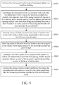
- FIG. 5 is a flow chart a method for manufacturing an electronic device according to the third embodiment of the present disclosure.
- FIG. 6 is a flow chart a method for manufacturing an electronic device according to the fourth embodiment of the present disclosure.
- FIG. 7 is a flow chart a method for manufacturing an electronic device according to the fifth embodiment of the present disclosure.
- FIG. 8 is a flow chart a method for manufacturing an electronic device according to the sixth embodiment of the present disclosure.
- Step 101 is forming a first shell and a second shell made of transparent plastic via injection molding.
- Step 102 is assembling the first shell and the second shell with each other via adhesives to form a casing for receiving an electronic module, two opposite ends of the casing respectively having a first opening and a second opening, the first opening and second opening aligned with each other along an extending direction, a seam located at an outer surface of the casing and between the first shell and the second shell.
- Step 103 is grinding the outer surface of the casing.
- Step 104 is painting a layer of black-out paint and a layer of primer paint on the outer surface of the casing sequentially to form a paint level for covering the seam.
- Step 105 is removing a part of the paint level via lasers to uncover a region of the casing which lights emitted by the electronic module can pass through.
- Step 106 is painting a decorative paint around the first opening and the second opening, wherein a color of the decorative paint is deeper than a color of the layer of primer paint.
- a material of the layer of black-out layer is a black paint
- a material of the layer of primer paint is a wood paint whose color is similar to a real wood (such as Thuja or Rosewood)
- a material of the decorative paint is a wood paint whose color is deeper than the color of the layer of primer paint.
- FIG. 2( a ) is a schematic view of assembling a first shell and a second shell with each other to form a casing for receiving an electronic module based on FIG. 1 .
- left and right ends of a first shell 102 respective have a first groove 1022 and a second groove 1024
- the left and right ends of a second shell 104 respectively have a third groove 1042 and a fourth groove 1044 .
- the location of the first groove 1022 corresponds to the location of the third groove 1042
- the location of the second groove 1024 corresponds to the location of the fourth groove 1044 .
- An electronic module 106 is disposed between the first shell 102 and the second shell 104 , the electronic module 106 has a channel 1062 and a light source 1064 , and the light source 1064 can be exemplary a light-emitting diode.
- FIG. 2( b ) is a schematic view of grinding an outer surface of a casing and forming a paint level on an outer surface of the casing based on FIG. 1 . As shown in FIG.
- the first groove 1022 of the first shell 102 is connected with the third groove 1042 of the second shell 104 to form a first opening 108 which is located at the left end of the casing 100
- the second groove 1024 of the first shell 102 is connected with the fourth groove 1044 of the second shell 104 to form a second opening 110 which is located at the right end of the casing 100
- the first opening 108 and the second opening 110 are aligned with each other along an extending direction.
- the channel 1062 of the electronic module 106 can be exemplary a straight channel or a curved channel, and only the left and the right ends of the channel 1062 are respectively aligned with the first opening 108 and the second opening 110 .
- a seam which is located at the outer surface of the casing 100 and between the first shell 102 and the second shell 104 can be completely covered by the paint level 112 .
- FIG. 2( c ) is a schematic view of removing a part of a paint level via lasers to uncover a region of a casing based on FIG. 1 .
- a part of the paint level 112 is removed to uncover a first region 114 of the casing 100
- the light source 1064 of the electronic module 106 faces the first region 114 of the casing 100 .
- lights emitted by the light source 1064 can pass through the first region 114 to indicate an operation state of the electronic module 106 .
- FIG. 2 ( d ) is a schematic view of painting a decorative paint on a casing based on FIG. 1 .
- a decorative paint 120 is respectively painted on a second region 116 and a third region 118 of the paint level 112 which are respectively around the first opening 108 and the second opening 110 , and a color of the decorative paint 120 is deeper than a color of the paint level 112 , which imitates a color of a real wood and grains of a real wood.
- FIG. 2( e ) is a schematic view of a water transferring process implemented on a casing based on FIG. 1 .
- the first opening 108 and the second opening 110 of the casing 100 are aligned with each other along an extending direction Y, and the extending direction Y is vertical to the water transferring film 122 .
- the casing 100 is moved toward the water transferring film 122 , which makes that the paint level 112 is connected with the water transferring film 122 .
- FIG. 2 ( f ) is a schematic view of connecting a water transferring film with a paint level based on FIG. 1 .
- grains of the water transferring film 122 are similar to grains of a real wood.
- the paint level 112 of the casing 100 has grains which are similar to grains of a real wood.
- FIGS. 3( a ) to 3( d ) illustrate steps of a water transferring process implemented on a casing.
- a fixture 124 is fixed with the casing 100 via the first opening 108 or the second opening 110 , and the extending direction Y of the first opening 108 (or the second opening 110 ) is vertical to the water transferring film 122 floated on water.
- the fixture 124 drives the casing 100 to move downward toward the water transferring film 122 , which makes that the casing 100 is connected with the water transferring film 122 .
- FIG. 3( a ) illustrate steps of a water transferring process implemented on a casing.
- the casing 100 completely enters into water to connect with the water transferring film 122 .
- the fixture 124 drives the casing 100 to move upward, which makes that the casing 100 completely leaves from water.
- FIG. 4 is a flow chart a method for manufacturing an electronic device according to the second embodiment of the present disclosure.
- a difference between the second embodiment and the first embodiment is that a light diffusion agent is added to the transparent plastic before forming the first shell 102 and second shell 104 made of the transparent plastic via injection molding. Adding the light diffusion agent to the transparent plastic before forming the first shell 102 and second shell 104 made of the transparent plastic via injection molding, which makes that lights passing through the casing 100 are more uniform.
- FIG. 5 is a flow chart a method for manufacturing an electronic device according to the third embodiment of the present disclosure. As shown in FIG. 5 , a difference between the third embodiment and the first embodiment is that grinding the outer surface of the casing 100 is omitted.
- FIG. 6 is a flow chart a method for manufacturing an electronic device according to the fourth embodiment of the present disclosure.
- differences between the fourth embodiment and the first embodiment are that a material of the first shell 102 and a material of the second shell 104 are not limited and removing a part of paint level 112 is omitted.
- the electronic module 106 is not provided with the light source 1064 , the casing 100 which lights can pass through is not necessary so that forming the casing 100 made of the transparent plastic via injection molding and removing a part of the paint level 112 are not necessary.
- FIG. 7 is a flow chart a method for manufacturing an electronic device according to the fifth embodiment of the present disclosure. As shown in FIG. 7 , a difference between the fifth embodiment and the first embodiment is that an ultraviolet curing paint is painted on the water transferring film 112 to form a transparent protection layer for imitating shines of a natural material after the water transferring film 122 is connected with the paint level 112 .
- FIG. 8 is a flow chart a method for manufacturing an electronic device according to the sixth embodiment of the present disclosure. As shown in FIG. 8 , differences between the sixth embodiment and the first embodiment are that an ultraviolet curing paint is painted on the water transferring film 112 to form a transparent protection layer and an ultraviolet light source is used for drying the water transferring film 112 and the ultraviolet curing paint after the water transferring film 122 is connected with the paint level 112 .
- first shell 102 and the second shell 104 respectively have the first opening 108 and the second opening 108 before the first shell 102 and the second shell 104 are assembled with each other.
- painting the decorative paint 120 is omitted, which makes that the paint level 112 formed on the outer surface of the casing 100 only includes the layer of primer paint.
- the color of the layer of primer paint is similar to a color of a real jade or a color of any one natural material
- the color of the decorative paint is also similar to a color of a real jade or a color of any one natural material.
- the grains of the water transferring film 122 are similar to grains of a jade or grains of any one natural material.
- the shape of the casing made by the method of the present disclosure is not limited, the casing can be exemplary a circular shaped casing or a polygon shaped casing.
- the method of the present disclosure is capable of maintaining original functions of the electronic device.
- the decorative paint whose color is deeper than the color of the layer of primer paint is painted around the first opening and the second opening, which imitates a gradient color of any natural material.
- the water transferring process makes the grains of the paint level are similar to grains of any one natural material and makes the appearance of the electronic device imitates an appearance of any one natural material.
Landscapes
- Engineering & Computer Science (AREA)
- Microelectronics & Electronic Packaging (AREA)
- Life Sciences & Earth Sciences (AREA)
- Wood Science & Technology (AREA)
- Physics & Mathematics (AREA)
- Health & Medical Sciences (AREA)
- General Health & Medical Sciences (AREA)
- Optics & Photonics (AREA)
- Toxicology (AREA)
- Application Of Or Painting With Fluid Materials (AREA)
Abstract
Description
Claims (15)
Applications Claiming Priority (3)
| Application Number | Priority Date | Filing Date | Title |
|---|---|---|---|
| CN201810152032.1 | 2018-02-14 | ||
| CN201810152032.1A CN110154619A (en) | 2018-02-14 | 2018-02-14 | The manufacturing method of electronic device |
| CN201810152032 | 2018-02-14 |
Publications (2)
| Publication Number | Publication Date |
|---|---|
| US20190254183A1 US20190254183A1 (en) | 2019-08-15 |
| US10863636B2 true US10863636B2 (en) | 2020-12-08 |
Family
ID=67540387
Family Applications (1)
| Application Number | Title | Priority Date | Filing Date |
|---|---|---|---|
| US16/173,068 Active 2039-08-14 US10863636B2 (en) | 2018-02-14 | 2018-10-29 | Method for manufacturing electronic device |
Country Status (2)
| Country | Link |
|---|---|
| US (1) | US10863636B2 (en) |
| CN (1) | CN110154619A (en) |
Families Citing this family (1)
| Publication number | Priority date | Publication date | Assignee | Title |
|---|---|---|---|---|
| CN110191600A (en) * | 2019-05-29 | 2019-08-30 | 英业达科技有限公司 | Wearable electronic device |
Citations (5)
| Publication number | Priority date | Publication date | Assignee | Title |
|---|---|---|---|---|
| US20130280463A1 (en) * | 2012-04-20 | 2013-10-24 | Skinit, Inc. | Display protector for consumer products with customizable appearance and methods relating to same |
| US9039264B2 (en) * | 2012-06-04 | 2015-05-26 | New Tsai Capital, Llc | Ornament with enclosed water-proof battery capsule |
| US9932133B2 (en) * | 2015-01-23 | 2018-04-03 | Hot Girls Pearls Inc. | Therapeutic jewelry |
| US10617023B2 (en) * | 2018-06-01 | 2020-04-07 | Inventec (Pudong) Technology Corporation | Wearable electronic device |
| US10632777B2 (en) * | 2014-12-01 | 2020-04-28 | Taica Corporation | Water pressure transfer method and water pressure transfer film |
Family Cites Families (5)
| Publication number | Priority date | Publication date | Assignee | Title |
|---|---|---|---|---|
| CN201099117Y (en) * | 2007-08-28 | 2008-08-13 | 汉达精密电子(昆山)有限公司 | Water transfer printing fixture |
| CN103253066B (en) * | 2012-02-16 | 2016-04-20 | 汉达精密电子(昆山)有限公司 | Exterior decorative effect processing method and products thereof |
| JP6473579B2 (en) * | 2014-06-24 | 2019-02-20 | シャープ株式会社 | Housing, display device, and bathroom |
| KR102247283B1 (en) * | 2014-10-20 | 2021-05-03 | 삼성전자주식회사 | Electronic device and fabrication method for exterior member of the same |
| CN206559778U (en) * | 2017-02-23 | 2017-10-13 | 速码波科技股份有限公司 | Metal shell structure |
-
2018
- 2018-02-14 CN CN201810152032.1A patent/CN110154619A/en active Pending
- 2018-10-29 US US16/173,068 patent/US10863636B2/en active Active
Patent Citations (5)
| Publication number | Priority date | Publication date | Assignee | Title |
|---|---|---|---|---|
| US20130280463A1 (en) * | 2012-04-20 | 2013-10-24 | Skinit, Inc. | Display protector for consumer products with customizable appearance and methods relating to same |
| US9039264B2 (en) * | 2012-06-04 | 2015-05-26 | New Tsai Capital, Llc | Ornament with enclosed water-proof battery capsule |
| US10632777B2 (en) * | 2014-12-01 | 2020-04-28 | Taica Corporation | Water pressure transfer method and water pressure transfer film |
| US9932133B2 (en) * | 2015-01-23 | 2018-04-03 | Hot Girls Pearls Inc. | Therapeutic jewelry |
| US10617023B2 (en) * | 2018-06-01 | 2020-04-07 | Inventec (Pudong) Technology Corporation | Wearable electronic device |
Also Published As
| Publication number | Publication date |
|---|---|
| US20190254183A1 (en) | 2019-08-15 |
| CN110154619A (en) | 2019-08-23 |
Similar Documents
| Publication | Publication Date | Title |
|---|---|---|
| US8597009B2 (en) | Film insert molding (FIM) on a 3D shape | |
| CN110758001A (en) | Housing, electronic device, and method of manufacturing the housing | |
| US9188737B2 (en) | Physical texture digital display system | |
| US10863636B2 (en) | Method for manufacturing electronic device | |
| CN205245032U (en) | Vapour door handle modulated structure with radium carving pattern | |
| CN102442031A (en) | Marble surface imitated glass fiber reinforced plastic product and preparation method thereof | |
| TWI702155B (en) | Method for manufacturing shell of electronic device | |
| CN1905783A (en) | Portable electronic apparatus with colour change function | |
| CN108682296A (en) | A kind of the electric appliance display panel and its processing method of stealthy display | |
| CN102170761B (en) | Combined snap joint structure and portable mobile terminal | |
| CN202302950U (en) | Strip | |
| CN211138892U (en) | Stone decorative board | |
| US7762710B2 (en) | Structure in the outer enveloping shells of christmas lamps | |
| CN105818509A (en) | Glass bead film, shell using same, and manufacturing technology of shell | |
| CN221892891U (en) | Resin artwork with built-in spotlight | |
| CN206036826U (en) | Decorate diamond lamp | |
| WO2004093127A3 (en) | Lamp system for curing resin in glass | |
| CN106733550B (en) | Method for realizing three-dimensional spray painting automobile decorative product | |
| CN214901257U (en) | TWS earphone charging box with good luminous effect | |
| CN111163602A (en) | Shell assembly, preparation method thereof and electronic equipment | |
| US20250216065A1 (en) | String lamp housing structure | |
| WO2013186578A1 (en) | Decorative transparent insert and the mode of proceeding | |
| KR200363416Y1 (en) | decoration with stained glass | |
| CN209295017U (en) | A kind of headlight | |
| CN113561546B (en) | Electronic equipment shell manufacturing process, electronic equipment shell and electronic equipment |
Legal Events
| Date | Code | Title | Description |
|---|---|---|---|
| AS | Assignment |
Owner name: INVENTEC (PUDONG) TECHNOLOGY CORPORATION, CHINA Free format text: ASSIGNMENT OF ASSIGNORS INTEREST;ASSIGNORS:LIN, CHUN-CHI;CHEN, YING-SHAN;CHEN, I-FANG;REEL/FRAME:047337/0091 Effective date: 20181022 Owner name: INVENTEC CORPORATION, TAIWAN Free format text: ASSIGNMENT OF ASSIGNORS INTEREST;ASSIGNORS:LIN, CHUN-CHI;CHEN, YING-SHAN;CHEN, I-FANG;REEL/FRAME:047337/0091 Effective date: 20181022 |
|
| FEPP | Fee payment procedure |
Free format text: ENTITY STATUS SET TO UNDISCOUNTED (ORIGINAL EVENT CODE: BIG.); ENTITY STATUS OF PATENT OWNER: LARGE ENTITY |
|
| STPP | Information on status: patent application and granting procedure in general |
Free format text: NOTICE OF ALLOWANCE MAILED -- APPLICATION RECEIVED IN OFFICE OF PUBLICATIONS |
|
| STCF | Information on status: patent grant |
Free format text: PATENTED CASE |
|
| MAFP | Maintenance fee payment |
Free format text: PAYMENT OF MAINTENANCE FEE, 4TH YEAR, LARGE ENTITY (ORIGINAL EVENT CODE: M1551); ENTITY STATUS OF PATENT OWNER: LARGE ENTITY Year of fee payment: 4 |