US10862043B2 - Organic light-emitting device - Google Patents
Organic light-emitting device Download PDFInfo
- Publication number
- US10862043B2 US10862043B2 US15/140,417 US201615140417A US10862043B2 US 10862043 B2 US10862043 B2 US 10862043B2 US 201615140417 A US201615140417 A US 201615140417A US 10862043 B2 US10862043 B2 US 10862043B2
- Authority
- US
- United States
- Prior art keywords
- group
- substituted
- unsubstituted
- salt
- layer
- Prior art date
- Legal status (The legal status is an assumption and is not a legal conclusion. Google has not performed a legal analysis and makes no representation as to the accuracy of the status listed.)
- Active, expires
Links
Images


Classifications
-
- H—ELECTRICITY
- H10—SEMICONDUCTOR DEVICES; ELECTRIC SOLID-STATE DEVICES NOT OTHERWISE PROVIDED FOR
- H10K—ORGANIC ELECTRIC SOLID-STATE DEVICES
- H10K85/00—Organic materials used in the body or electrodes of devices covered by this subclass
- H10K85/60—Organic compounds having low molecular weight
- H10K85/631—Amine compounds having at least two aryl rest on at least one amine-nitrogen atom, e.g. triphenylamine
- H10K85/636—Amine compounds having at least two aryl rest on at least one amine-nitrogen atom, e.g. triphenylamine comprising heteroaromatic hydrocarbons as substituents on the nitrogen atom
-
- H01L51/0061—
-
- H01L51/0059—
-
- H01L51/006—
-
- H01L51/0067—
-
- H01L51/0072—
-
- H01L51/0073—
-
- H—ELECTRICITY
- H10—SEMICONDUCTOR DEVICES; ELECTRIC SOLID-STATE DEVICES NOT OTHERWISE PROVIDED FOR
- H10K—ORGANIC ELECTRIC SOLID-STATE DEVICES
- H10K85/00—Organic materials used in the body or electrodes of devices covered by this subclass
- H10K85/60—Organic compounds having low molecular weight
- H10K85/631—Amine compounds having at least two aryl rest on at least one amine-nitrogen atom, e.g. triphenylamine
- H10K85/633—Amine compounds having at least two aryl rest on at least one amine-nitrogen atom, e.g. triphenylamine comprising polycyclic condensed aromatic hydrocarbons as substituents on the nitrogen atom
-
- H—ELECTRICITY
- H10—SEMICONDUCTOR DEVICES; ELECTRIC SOLID-STATE DEVICES NOT OTHERWISE PROVIDED FOR
- H10K—ORGANIC ELECTRIC SOLID-STATE DEVICES
- H10K85/00—Organic materials used in the body or electrodes of devices covered by this subclass
- H10K85/60—Organic compounds having low molecular weight
- H10K85/649—Aromatic compounds comprising a hetero atom
- H10K85/654—Aromatic compounds comprising a hetero atom comprising only nitrogen as heteroatom
-
- H—ELECTRICITY
- H10—SEMICONDUCTOR DEVICES; ELECTRIC SOLID-STATE DEVICES NOT OTHERWISE PROVIDED FOR
- H10K—ORGANIC ELECTRIC SOLID-STATE DEVICES
- H10K85/00—Organic materials used in the body or electrodes of devices covered by this subclass
- H10K85/60—Organic compounds having low molecular weight
- H10K85/649—Aromatic compounds comprising a hetero atom
- H10K85/657—Polycyclic condensed heteroaromatic hydrocarbons
- H10K85/6572—Polycyclic condensed heteroaromatic hydrocarbons comprising only nitrogen in the heteroaromatic polycondensed ring system, e.g. phenanthroline or carbazole
-
- H—ELECTRICITY
- H10—SEMICONDUCTOR DEVICES; ELECTRIC SOLID-STATE DEVICES NOT OTHERWISE PROVIDED FOR
- H10K—ORGANIC ELECTRIC SOLID-STATE DEVICES
- H10K85/00—Organic materials used in the body or electrodes of devices covered by this subclass
- H10K85/60—Organic compounds having low molecular weight
- H10K85/649—Aromatic compounds comprising a hetero atom
- H10K85/657—Polycyclic condensed heteroaromatic hydrocarbons
- H10K85/6574—Polycyclic condensed heteroaromatic hydrocarbons comprising only oxygen in the heteroaromatic polycondensed ring system, e.g. cumarine dyes
-
- H01L51/0052—
-
- H01L51/0085—
-
- H01L51/5064—
-
- H—ELECTRICITY
- H10—SEMICONDUCTOR DEVICES; ELECTRIC SOLID-STATE DEVICES NOT OTHERWISE PROVIDED FOR
- H10K—ORGANIC ELECTRIC SOLID-STATE DEVICES
- H10K50/00—Organic light-emitting devices
- H10K50/10—OLEDs or polymer light-emitting diodes [PLED]
- H10K50/14—Carrier transporting layers
- H10K50/15—Hole transporting layers
- H10K50/156—Hole transporting layers comprising a multilayered structure
-
- H—ELECTRICITY
- H10—SEMICONDUCTOR DEVICES; ELECTRIC SOLID-STATE DEVICES NOT OTHERWISE PROVIDED FOR
- H10K—ORGANIC ELECTRIC SOLID-STATE DEVICES
- H10K85/00—Organic materials used in the body or electrodes of devices covered by this subclass
- H10K85/30—Coordination compounds
- H10K85/341—Transition metal complexes, e.g. Ru(II)polypyridine complexes
- H10K85/342—Transition metal complexes, e.g. Ru(II)polypyridine complexes comprising iridium
-
- H—ELECTRICITY
- H10—SEMICONDUCTOR DEVICES; ELECTRIC SOLID-STATE DEVICES NOT OTHERWISE PROVIDED FOR
- H10K—ORGANIC ELECTRIC SOLID-STATE DEVICES
- H10K85/00—Organic materials used in the body or electrodes of devices covered by this subclass
- H10K85/60—Organic compounds having low molecular weight
- H10K85/615—Polycyclic condensed aromatic hydrocarbons, e.g. anthracene
Definitions
- One or more aspects of embodiments of the present disclosure relate to an organic light-emitting device.
- Organic light-emitting devices are self-emission devices that have wide viewing angles, high contrast ratios, short response times, and excellent brightness, driving voltage, and response speed characteristics, and can produce full-color images.
- the organic light-emitting device may include a first electrode disposed (e.g., positioned) on a substrate, and a hole transport region, an emission layer, an electron transport region, and a second electrode, which are sequentially disposed on the first electrode. Holes provided from the first electrode may move toward the emission layer through the hole transport region, and electrons provided from the second electrode may move toward the emission layer through the electron transport region. Carriers, such as holes and electrons, may then recombine in the emission layer to produce excitons. These excitons transition from an excited state to a ground state, thereby generating light.
- One or more aspects of embodiments of the present disclosure are directed toward an organic light-emitting device having low driving voltage and high efficiency.
- an organic light-emitting device includes:
- the hole transport region includes a first compound represented by Formula 1 and a second compound represented by Formula 2:
- X 1 may be selected from N-(L 6 ) a6 -(Ar 3 ) b3 , O, and S,
- X 2 may be selected from N-(L 7 ) a7 -(Ar 4 ) b4 , O, and S,
- X 3 and X 11 may each independently be selected from nitrogen (N), boron (B), and phosphorous (P),
- A may be a substituted or unsubstituted C 6 -C 20 aromatic ring
- L 1 to L 7 , L 11 to L 13 , and L 21 may each independently be selected from a substituted or unsubstituted C 3 -C 10 cycloalkylene group, a substituted or unsubstituted C 1 -C 10 heterocycloalkylene group, a substituted or unsubstituted C 3 -C 10 cycloalkenylene group, a substituted or unsubstituted C 1 -C 10 heterocycloalkenylene group, a substituted or unsubstituted C 6 -C 60 arylene group, a substituted or unsubstituted C 1 -C 60 heteroarylene group, a substituted or unsubstituted divalent non-aromatic condensed polycyclic group, and a substituted or unsubstituted divalent non-aromatic condensed heteropolycyclic group,
- a1 to a7, a11 to a13, and a21 may each independently be an integer selected from 0 to 3,
- Ar 1 to Ar 4 , Ar 11 , and Ar 21 may each independently be selected from a substituted or unsubstituted C 3 -C 10 cycloalkyl group, a substituted or unsubstituted C 1 -C 10 heterocycloalkyl group, a substituted or unsubstituted C 3 -C 10 cycloalkenyl group, a substituted or unsubstituted C 1 -C 10 heterocycloalkenyl group, a substituted or unsubstituted C 6 -C 60 aryl group, a substituted or unsubstituted C 1 -C 60 heteroaryl group, a substituted or unsubstituted monovalent non-aromatic condensed polycyclic group, and a substituted or unsubstituted monovalent non-aromatic condensed heteropolycyclic group,
- b1 to b4, b11, and b21 may each independently be an integer selected from 1 to 5,
- R 1 to R 4 and R 11 to R 16 may each independently be selected from hydrogen, deuterium, —F, —Cl, —Br, —I, a hydroxyl group, a cyano group, a nitro group, an amino group, an amidino group, a hydrazine group, a hydrazone group, a carboxylic acid group or a salt thereof, a sulfonic acid group or a salt thereof, a phosphoric acid group or a salt thereof, a substituted or unsubstituted C 1 -C 60 alkyl group, a substituted or unsubstituted C 2 -C 60 alkenyl group, a substituted or unsubstituted C 2 -C 60 alkynyl group, a substituted or unsubstituted C 1 -C 60 alkoxy group, a substituted or unsubstituted C 3 -C 10 cycloalkyl group, a substituted or unsubstit
- c1, c3, c11, and c13 may each independently be an integer selected from 1 to 4, and c2, c4, c12, and c14 may each independently be an integer selected from 1 to 3, and
- the substituted C 6 -C 20 aromatic ring the substituted C 3 -C 10 cycloalkylene group, the substituted C 1 -C 10 heterocycloalkylene group, the substituted C 3 -C 10 cycloalkenylene group, the substituted C 1 -C 10 heterocycloalkenylene group, the substituted C 6 -C 60 arylene group, the substituted C 1 -C 60 heteroarylene group, the substituted divalent non-aromatic condensed polycyclic group, the substituted divalent non-aromatic condensed heteropolycyclic group, the substituted C 1 -C 60 alkyl group, the substituted C 2 -C 60 alkenyl group, the substituted C 2 -C 60 alkynyl group, the substituted C 1 -C 60 alkoxy group, the substituted C 3 -C 10 cycloalkyl group, the substituted C 1 -C 10 heterocycloalkyl group, the substituted C 3 -
- deuterium —F, —Cl, —Br, —I, a hydroxyl group, a cyano group, a nitro group, an amino group, an amidino group, a hydrazine group, a hydrazone group, a carboxylic acid group or a salt thereof, a sulfonic acid group or a salt thereof, a phosphoric acid group or a salt thereof, a C 1 -C 60 alkyl group, a C 2 -C 60 alkenyl group, a C 2 -C 60 alkynyl group, and a C 1 -C 60 alkoxy group;
- Q 1 to Q 5 , Q 11 to Q 15 , Q 21 to Q 25 , and Q 31 to Q 35 may each independently be selected from hydrogen, deuterium, —F, —Cl, —Br, —I, a hydroxyl group, a cyano group, a nitro group, an amino group, an amidino group, a hydrazine group, a hydrazone group, a carboxylic acid group or a salt thereof, a sulfonic acid group or a salt thereof, a phosphoric acid group or a salt thereof, a C 1 -C 60 alkyl group, a C 2 -C 60 alkenyl group, a C 2 -C 60 alkynyl group, a C 1 -C 60 alkoxy group, a C 3 -C 10 cycloalkyl group, a C 1 -C 10 heterocycloalkyl group, a C 3 -C 10 cycloalkenyl group, a C 1
- the drawing is a schematic view of an organic light-emitting device 10 according to an embodiment.
- the organic light-emitting device 10 may include a first electrode 110 , a hole transport region 130 , an emission layer 150 , an electron transport region 170 , and a second electrode 190 .
- a substrate may be additionally disposed (e.g., positioned) under the first electrode 110 or above the second electrode 190 .
- the substrate may be a glass substrate or a transparent plastic substrate, each having excellent mechanical strength, thermal stability, transparency, surface smoothness, ease of handling, and/or water-resistance.
- the first electrode 110 may be formed by depositing or sputtering a material for forming the first electrode 110 on the substrate.
- the material for forming the first electrode 110 may be selected from materials with a high work function to facilitate hole injection.
- the first electrode 110 may be a reflective electrode, a semi-transmissive electrode, or a transmissive electrode.
- the material for forming the first electrode may be a transparent and/or highly conductive material, and non-limiting examples of such material include indium tin oxide (ITO), indium zinc oxide (IZO), tin oxide (SnO 2 ), and zinc oxide (ZnO).
- the first electrode 110 is a semi-transmissive electrode or a reflective electrode
- a material for forming the first electrode 110 at least one selected from magnesium (Mg), aluminum (Al), aluminum-lithium (Al—Li), calcium (Ca), magnesium-indium (Mg—In), and magnesium-silver (Mg—Ag) may be used.
- the first electrode 110 may have a single-layered structure, or a multi-layered structure including two or more layers.
- the first electrode 110 may have a three-layered structure of ITO/Ag/ITO, but the structure of the first electrode 110 is not limited thereto.
- the hole transport region 130 , the emission layer 150 , and the electron transport region 170 may be sequentially stacked in this stated order.
- the hole transport region 130 may include a first compound represented by Formula 1 and a second compound represented by Formula 2:
- X 1 may be selected from N-(L 6 ) a6 -(Ar 3 ) b3 , O, and S;
- X 2 may be selected from N-(L 7 ) a7 -(Ar 4 ) b4 , O, and S;
- X 3 and X 11 may each independently be selected from nitrogen (N), boron (B), and phosphorous (P).
- X 1 and X 2 in Formulae 1 and 2 may each independently be selected from O and S.
- X 1 and X 2 may be identical to or different from each other.
- X 1 and X 2 may be identical to each other.
- a in Formula 1 may be a substituted or unsubstituted C 6 -C 20 aromatic ring.
- a in Formula 1 may be selected from a substituted or unsubstituted benzene group, a substituted or unsubstituted naphthalene group, a substituted or unsubstituted anthracene group, a substituted or unsubstituted pyrene group, a substituted or unsubstituted phenanthrene group, a substituted or unsubstituted chrysene group, and a substituted or unsubstituted triphenylene group.
- a in Formula 1 may be a group represented by one selected from Formulae 2-1 to 2-19:
- Z 21 and Z 22 may each independently be selected from hydrogen, deuterium, —F, —Cl, —Br, —I, a hydroxyl group, a cyano group, a nitro group, an amino group, an amidino group, a hydrazine group, a hydrazone group, a carboxylic acid group or a salt thereof, a sulfonic acid group or a salt thereof, a phosphoric acid group or a salt thereof, a C 1 to C 20 alkyl group, a C 1 to C 20 alkoxy group, a phenyl group, a naphthyl group, a fluorenyl group, a spiro-fluorenyl group, a benzofluorenyl group, a dibenzofluorenyl group, a phenanthrenyl group, an anthracenyl group, a pyrenyl group, a chrysenyl group, a pyri
- f1 may be 1 or 2
- f2 may be an integer selected from 1 to 3
- f3 may be an integer selected from 1 to 4
- f4 may be an integer selected from 1 to 5
- f5 may be an integer selected from 1 to 7 and
- * and *′ each independently indicate a binding site to a neighboring atom
- *′′ indicates a binding site to L 3 or X 3 in Formula 1.
- a in Formula 1 may be a group represented by Formula 2-1.
- L 1 to L 7 , L 11 to L 13 , and L 21 in Formulae 1 and 2 may each independently be selected from a substituted or unsubstituted C 3 -C 10 cycloalkylene group, a substituted or unsubstituted C 1 -C 10 heterocycloalkylene group, a substituted or unsubstituted C 3 -C 10 cycloalkenylene group, a substituted or unsubstituted C 1 -C 10 heterocycloalkenylene group, a substituted or unsubstituted C 6 -C 60 arylene group, a substituted or unsubstituted C 1 -C 60 heteroarylene group, a substituted or unsubstituted divalent non-aromatic condensed polycyclic group, and a substituted or unsubstituted divalent non-aromatic condensed heteropolycyclic group.
- L 1 to L 7 , L 11 to L 13 , and L 21 in Formulae 1 and 2 may each independently be selected from the group consisting of:
- L 1 to L 7 , L 11 to L 13 , and L 21 in Formulae 1 and 2 may each independently be selected from groups represented by Formulae 3-1 to 3-42:
- Y 1 may be selected from O, S, C(Z 3 )(Z 4 ), N(Z 5 ), and Si(Z 6 )(Z 7 ),
- Z 1 to Z 7 may each independently be selected from hydrogen, deuterium, —F, —Cl, —Br, —I, a hydroxyl group, a cyano group, a nitro group, an amino group, an amidino group, a hydrazine group, a hydrazone group, a carboxylic acid group or a salt thereof, a sulfonic acid group or a salt thereof, a phosphoric acid group or a salt thereof, a C 1 to C 20 alkyl group, a C 1 to C 20 alkoxy group, a phenyl group, a naphthyl group, a fluorenyl group, a spiro-fluorenyl group, a benzofluorenyl group, a dibenzofluorenyl group, a phenanthrenyl group, an anthracenyl group, a pyrenyl group, a chrysenyl group, a pyri
- d2 may be 1 or 2
- d3 may be an integer selected from 1 to 3,
- d4 may be an integer selected from 1 to 4,
- d5 may be an integer selected from 1 to 5
- d6 may be an integer selected from 1 to 6,
- d8 may be an integer selected from 1 to 8, and
- * and *′ each independently indicate a binding site to a neighboring atom.
- L 1 to L 7 , L 11 to L 13 , and L 21 in Formulae 1 and 2 may each independently be selected from groups represented by Formulae 4-1 to 4-36:
- * and *′ in Formulae 4-1 to 4-36 each independently indicate a binding site to a neighboring atom, and “D” may refer to deuterium.
- a1 to a7, a11 to a13, and a21 in Formulae 1 and 2 may each independently be an integer selected from 0 to 3.
- a1 indicates the number of L 1 (s), wherein when a1 is zero, -(L 1 ) a1 - may be a single bond, and when a1 is two or more, two or more L 1 (s) may be identical to or different from each other.
- Descriptions of a2 to a7, a11 to a13, and a21 may be understood by referring to the description provided in connection with a1 and the corresponding structures of Formulae 1 and 2.
- a1, a2, a4, a5 to a7, a12, a13, and a21 may each independently be 0 or 1, and a3 and a11 may each independently be 1 or 2.
- a1, a2, a4, a5 to a7, a12, a13, and a21 may be 0, a3 may be 1 or 2, and a11 may be 1, but embodiments are not limited thereto.
- Ar 1 to Ar 4 , Ar 11 , and Ar 21 in Formulae 1 and 2 may each independently be selected from a substituted or unsubstituted C 3 -C 10 cycloalkyl group, a substituted or unsubstituted C 1 -C 10 heterocycloalkyl group, a substituted or unsubstituted C 3 -C 10 cycloalkenyl group, a substituted or unsubstituted C 1 -C 10 heterocycloalkenyl group, a substituted or unsubstituted C 6 -C 60 aryl group, a substituted or unsubstituted C 1 -C 60 heteroaryl group, a substituted or unsubstituted monovalent non-aromatic condensed polycyclic group, and a substituted or unsubstituted monovalent non-aromatic condensed heteropolycyclic group.
- Ar 1 to Ar 4 , Ar 11 , and Ar 21 in Formulae 1 and 2 may each independently be selected from the group consisting of:
- Q 31 to Q 33 may each independently be selected from hydrogen, deuterium, —F, —Cl, —Br, —I, a hydroxyl group, a cyano group, a nitro group, an amino group, an amidino group, a hydrazine group, a hydrazone group, a carboxylic acid group or a salt thereof, a sulfonic acid group or a salt thereof, a phosphoric acid group or a salt thereof, a C 1 to C 20 alkyl group, a C 1 to C 20 alkoxy group, a phenyl group, a naphthyl group, a fluorenyl group, a spiro-fluorenyl group, a benzofluorenyl group, a dibenzofluorenyl group, a phenanthrenyl group, an anthracenyl group, a pyrenyl group, a chrysenyl group, a pyr
- Ar 1 to Ar 4 , Ar 11 , and Ar 21 in Formulae 1 and 2 may each independently be selected from groups represented by Formulae 5-1 to 5-81:
- Y 11 may be selected from O, S, C(Z 13 )(Z 14 ), N(Z 15 ), and Si(Z 16 )(Z 17 ),
- Z 11 to Z 17 may each independently be selected from hydrogen, deuterium, —F, —Cl, —Br, —I, a hydroxyl group, a cyano group, a nitro group, an amino group, an amidino group, a hydrazine group, a hydrazone group, a carboxylic acid group or a salt thereof, a sulfonic acid group or a salt thereof, a phosphoric acid group or a salt thereof, a C 1 -C 20 alkyl group, a C 1 -C 20 alkoxy group, a phenyl group, a naphthyl group, a fluorenyl group, a spiro-fluorenyl group, a benzofluorenyl group, a dibenzofluorenyl group, a phenanthrenyl group, an anthracenyl group, a pyrenyl group, a chrysenyl group, a
- Q 13 to Q 15 may each independently be selected from a C 1 -C 10 alkyl group, a C 1 -C 10 alkoxy group, a phenyl group, and a naphthyl group,
- e2 may be 1 or 2
- e3 may be an integer selected from 1 to 3,
- e4 may be an integer selected from 1 to 4,
- e5 may be an integer selected from 1 to 5
- e6 may be an integer selected from 1 to 6,
- e7 may be an integer selected from 1 to 7,
- e9 may be an integer selected from 1 to 9, and
- * indicates a binding site to a neighboring atom.
- Ar 1 to Ar 4 , Ar 11 , and Ar 21 in Formulae 1 and 2 may each independently be selected from groups represented by Formulae 6-1 to 6-158:
- * in Formulae 6-1 to 6-158 indicates a binding site to a neighboring atom, and “D” may refer to deuterium.
- b1 to b4, b11, and b21 in Formulae 1 and 2 may each independently be an integer selected from 1 to 5.
- b1 indicates the number of Ar 1 (s), wherein when b1 is two or more, two or more Ar 1 (s) may be identical to or different from each other.
- Descriptions of b2 to b4, b11, and b21 may be understood by referring to the description provided in connection with b1 and the corresponding structures of Formulae 1 and 2.
- b1 to b4, b11, and b21 may each independently be 1 or 2.
- b1 to b4, b11, and b21 may be 1, but are not limited thereto.
- R 1 to R 4 and R 11 to R 16 in Formulae 1 and 2 may each independently be selected from hydrogen, deuterium, —F, —Cl, —Br, —I, a hydroxyl group, a cyano group, a nitro group, an amino group, an amidino group, a hydrazine group, a hydrazone group, a carboxylic acid group or a salt thereof, a sulfonic acid group or a salt thereof, a phosphoric acid group or a salt thereof, a substituted or unsubstituted C 1 -C 60 alkyl group, a substituted or unsubstituted C 2 -C 60 alkenyl group, a substituted or unsubstituted C 2 -C 60 alkynyl group, a substituted or unsubstituted C 1 -C 60 alkoxy group, a substituted or unsubstituted C 3 -C 10 cycloalkyl group, a substitute
- R 1 to R 4 and R 11 to R 16 in Formulae 1 and 2 may each independently be selected from hydrogen, deuterium, —F, —Cl, —Br, —I, a hydroxyl group, a cyano group, a nitro group, an amino group, an amidino group, a hydrazine group, a hydrazone group, a carboxylic acid group or a salt thereof, a sulfonic acid group or a salt thereof, a phosphoric acid group or a salt thereof, a substituted or unsubstituted C 1 -C 20 alkyl group, a substituted or unsubstituted C 1 -C 20 alkoxy group, a substituted or unsubstituted C 6 -C 20 aryl group, a substituted or unsubstituted C 1 -C 20 heteroaryl group, a substituted or unsubstituted monovalent non-aromatic condensed polycyclic group, a substituted or
- R 1 to R 4 and R 11 to R 16 in Formulae 1 and 2 may each independently be selected from the group consisting of:
- Q 1 to Q 3 and Q 31 to Q 33 may each independently be selected from a C 1 -C 10 alkyl group, a C 1 -C 10 alkoxy group, a phenyl group, and a naphthyl group.
- R 1 to R 4 and R 11 to R 16 in Formulae 1 and 2 may each independently be selected from hydrogen, deuterium, —F, —Cl, —Br, —I, a hydroxyl group, a cyano group, a nitro group, an amino group, an amidino group, a hydrazine group, a hydrazone group, a carboxylic acid group or a salt thereof, a sulfonic acid group or a salt thereof, a phosphoric acid group or a salt thereof, a substituted or unsubstituted C 1 -C 20 alkyl group, and a substituted or unsubstituted C 1 -C 20 alkoxy group, but are not limited thereto.
- the first compound may be represented by one selected from Formulae 1A to 1 D
- the second compound may be represented by Formula 2A:
- X 1 to X 3 , X 11 , A, L 1 to L 7 , L 11 to L 13 , L 21 , a1 to a7, a11 to a13, a21, Ar 1 to Ar 4 , Ar 11 , Ar 21 , b1 to b4, b11, b21, R 1 to R 4 , R 11 to R 16 , c1 to c4, and c11 to c14 in Formulae 1A to 1D and 2A are the same as described herein.
- the first compound may be represented by one selected from Formulae 1A-1, 1B-1, 1C-1, and 1D-1
- the second compound may be represented by Formula 2A-1:
- the first compound may be represented by one selected from Formulae 1A-1(1), 1B-1(1), 1C-1(1), and 1D-1(1)
- the second compound may be represented by Formula 2A-1(1):
- X 1 and X 2 in Formulae 1A-1(1), 1B-1(1), 1C-1(1), and 1D-1(1) may each independently be selected from O and S,
- X 3 and X 11 may each independently be selected from N, B, and P,
- L 3 , L 6 , and L 7 may each independently be selected from groups represented by Formulae 4-1 to 4-36,
- Ar 1 , Ar 2 , Ar 11 , and Ar 21 may each independently be selected from Formulae 6-1 to 6-158, and
- R 15 and R 16 may each independently be selected from a methyl group and a phenyl group.
- the first compound may be one selected from Compounds 1 to 18, and the second compound may be one selected from Compounds 101 to 109, but embodiments are not limited thereto:
- the organic light-emitting device including the first compound and the second compound may have low driving voltage and high efficiency.
- the hole transport region 130 may include a hole transport layer, and a hole auxiliary layer between the hole transport layer and the emission layer.
- the first compound may be included in the hole auxiliary layer, and the second compound may be included in the hole transport layer.
- the hole auxiliary layer may directly contact the emission layer.
- a thickness of the hole auxiliary layer may be in a range of about 200 ⁇ to about 1,000 ⁇ , for example, about 250 ⁇ to about 450 ⁇ . When the thickness of the hole auxiliary layer is within any of these ranges, the hole transport layer may have satisfactory (or suitable) hole transport characteristics without a substantial increase in driving voltage.
- the hole transport region 130 may further include at least one selected from a hole injection layer, a hole transport layer, and a buffer layer, which are disposed between the anode and the hole auxiliary layer.
- the electron transport region 170 may include an electron auxiliary layer, and may further include at least one selected from an electron transport layer and an electron injection layer, which are disposed between the electron auxiliary layer and the cathode.
- the hole transport region 130 may have a structure of hole injection layer/hole transport layer/hole auxiliary layer, a structure of hole injection layer/hole transport layer/buffer layer/hole auxiliary layer, a structure of hole injection layer/hole auxiliary layer, a structure of hole injection layer/buffer layer/hole auxiliary layer, a structure of hole transport layer/hole auxiliary layer, or a structure of hole transport layer/buffer layer/hole auxiliary layer, wherein, in each of these structures, constituting layers are sequentially stacked in this stated order from the first electrode 110 .
- the structure of the hole transport region 130 is not limited thereto.
- the hole injection layer may be formed on the first electrode 110 by using one or more suitable methods such as vacuum deposition, spin coating, casting, langmuir-blodgett (LB) deposition, ink-jet printing, laser-printing, and/or laser-induced thermal imaging.
- suitable methods such as vacuum deposition, spin coating, casting, langmuir-blodgett (LB) deposition, ink-jet printing, laser-printing, and/or laser-induced thermal imaging.
- the vacuum deposition may be performed at a deposition temperature of about 100 to about 500° C., at a vacuum degree of about 10 ⁇ 8 to about 10 ⁇ 3 torr, and at a deposition rate of about 0.01 to about 100 ⁇ /sec, by taking into account a compound for forming the hole injection layer to be deposited and the structure of the hole injection layer to be formed.
- the spin coating may be performed at a coating rate of about 2,000 rpm to about 5,000 rpm, and at a temperature of about 80° C. to 200° C., by taking into account a compound for forming the hole injection layer to be deposited and the structure of the hole injection layer to be formed.
- a hole transport layer may be formed on the first electrode 110 or the hole injection layer by using one or more suitable methods such as vacuum deposition, spin coating, casting, an LB method, ink-jet printing, laser-printing, and/or laser-induced thermal imaging.
- suitable methods such as vacuum deposition, spin coating, casting, an LB method, ink-jet printing, laser-printing, and/or laser-induced thermal imaging.
- deposition and coating conditions for the hole transport layer may be the same as (or substantially similar to) the deposition and coating conditions for the hole injection layer.
- the hole transport region 130 may include at least one selected from the first compound represented by Formula 1 and the second compound represented by Formula 2.
- the first compound and the second compound may be the same as described above.
- the hole transport region may further include, in addition to the first compound and the second compound, at least one selected from m-MTDATA, TDATA, 2-TNATA, NPB, p-NPB, TPD, Spiro-TPD, Spiro-NPB, methylated NPB, TAPC, HMTPD, 4,4′,4′′-tris(N-carbazolyl)triphenylamine (TCTA), polyaniline/dodecylbenzenesulfonic acid (Pani/DBSA), poly(3,4-ethylenedioxythiophene)/poly(4-styrenesulfonate) (PEDOT/PSS), polyaniline/camphor sulfonic acid (Pani/CSA), and polyaniline/poly(4-styrenesulfonate) (PANI/PSS):
- a thickness of the hole transport region may be in a range of about 100 ⁇ to about 10,000 ⁇ , for example, about 100 ⁇ to about 1,000 ⁇ .
- a thickness of the hole injection layer may be in a range of about 100 ⁇ to about 10,000 ⁇ , for example, about 100 ⁇ to about 1,000 ⁇
- a thickness of the hole transport layer may be in a range of about 50 ⁇ to about 2,000 ⁇ , for example, about 100 ⁇ to about 1,500 ⁇ .
- the hole transport region may further include, in addition to the materials described above, a charge-generation material for the improvement of conductive properties.
- the charge-generation material may be homogeneously or non-homogeneously dispersed in the hole transport region.
- the charge-generation material may be, for example, a p-dopant.
- the p-dopant may be one selected from a quinone derivative, a metal oxide, and a cyano group-containing compound, but embodiments are not limited thereto.
- Non-limiting examples of the p-dopant include quinone derivatives (such as tetracyanoquinonedimethane (TCNQ) and/or 2,3,5,6-tetrafluoro-tetracyano-1,4-benzoquinonedimethane (F4-TCNQ)), metal oxides (such as tungsten oxide and/or molybdenum oxide), and Compound HT-D1 illustrated below, but are not limited thereto:
- the hole transport region may further include, in addition to the hole injection layer, the hole transport layer, and/or the hole auxiliary layer, at least one layer selected from a buffer layer and an electron blocking layer. Since the buffer layer may compensate for an optical resonance distance according to a wavelength of light emitted from the emission layer, light-emission efficiency of the formed organic light-emitting device may be improved. For use as a material included in the buffer layer, any of the materials that are to be included in the hole transport region may be used.
- the electron blocking layer may function to prevent or reduce the injection of electrons from the electron transport region.
- An emission layer may be formed on the first electrode 110 or the hole transport region by using one or more suitable methods such as vacuum deposition, spin coating, casting, an LB method, ink-jet printing, laser-printing, and/or laser-induced thermal imaging.
- suitable methods such as vacuum deposition, spin coating, casting, an LB method, ink-jet printing, laser-printing, and/or laser-induced thermal imaging.
- deposition and coating conditions for the emission layer may be the same as (or substantially similar to) those for the hole injection layer.
- the emission layer may be patterned into a red emission layer, a green emission layer, and/or a blue emission layer, according to a sub-pixel.
- the emission layer may have a stacked structure including a red emission layer, a green emission layer, and a blue emission layer, or may include a red-light emission material, a green-light emission material, and a blue-light emission material, which are mixed with each other in a single layer, to emit white light.
- the emission layer 150 may include a host and a dopant.
- the host may include a compound represented by Formula 301 below: Ar 301 -[(L 301 ) xb1 -R 301 ] xb2 .
- Formula 301 a compound represented by Formula 301 below: Ar 301 -[(L 301 ) xb1 -R 301 ] xb2 .
- Ar 301 may be selected from the group consisting of:
- L 301 may be the same as the description provided in connection with L 1 ,
- R 301 may be selected from the group consisting of:
- a C 1 -C 20 alkyl group and a C 1 -C 20 alkoxy group each substituted with at least one selected from deuterium, —F, —Cl, —Br, —I, a hydroxyl group, a cyano group, a nitro group, an amino group, an amidino group, a hydrazine group, a hydrazone group, a carboxylic acid group or a salt thereof, a sulfonic acid group or a salt thereof, a phosphoric acid group or a salt thereof, a phenyl group, a naphthyl group, a fluorenyl group, a spiro-fluorenyl group, a benzofluorenyl group, a dibenzofluorenyl group, a phenanthrenyl group, an anthracenyl group, a pyrenyl group, a chrysenyl group, a pyridinyl
- xb1 may be selected from 0, 1, 2, and 3, and
- xb2 may be selected from 1, 2, 3, and 4.
- L 301 may be selected from the group consisting of:
- a phenylene group a naphthylene group, a fluorenylene group, a spiro-fluorenylene group, a benzofluorenylene group, a dibenzofluorenylene group, a phenanthrenylene group, an anthracenylene group, a pyrenylene group, and a chrysenylene group;
- R 301 may be selected from the group consisting of:
- a C 1 -C 20 alkyl group and a C 1 -C 20 alkoxy group each substituted with at least one selected from deuterium, —F, —Cl, —Br, —I, a hydroxyl group, a cyano group, a nitro group, an amino group, an amidino group, a hydrazine group, a hydrazone group, a carboxylic acid group or a salt thereof, a sulfonic acid group or a salt thereof, a phosphoric acid group or a salt thereof, a phenyl group, a naphthyl group, a fluorenyl group, a spiro-fluorenyl group, a benzofluorenyl group, a dibenzofluorenyl group, a phenanthrenyl group, an anthracenyl group, a pyrenyl group, and a chrysenyl group;
- a phenyl group a naphthyl group, a fluorenyl group, a spiro-fluorenyl group, a benzofluorenyl group, a dibenzofluorenyl group, a phenanthrenyl group, an anthracenyl group, a pyrenyl group, and a chrysenyl group;
- the host may include a compound represented by Formula 301A below:
- the compound represented by Formula 301 may include at least one selected from Compounds H1 to H42, but is not limited thereto:
- the host may include at least one selected from Compounds H43 to H49 below, but is not limited thereto:
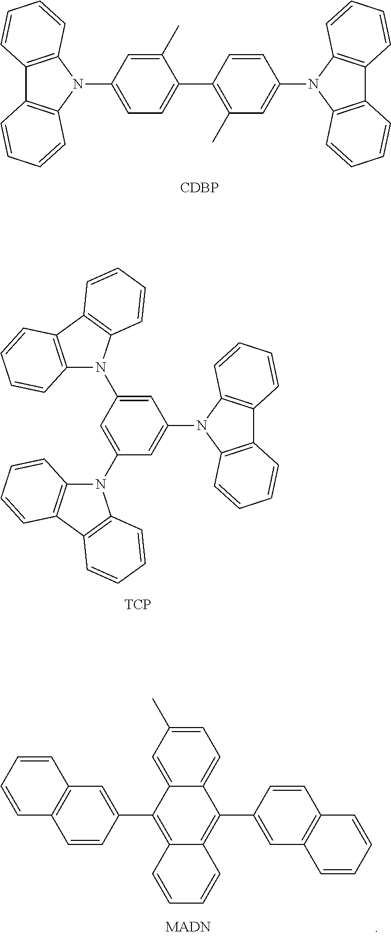
- the host may include one selected from the following compounds, but materials to be included in the host are not limited thereto:
- the dopant may include at least one selected from a fluorescent dopant and a phosphorescent dopant.
- the phosphorescent dopant may include an organometallic complex represented by Formula 401 below:
- M may be selected from iridium (Ir), platinum (Pt), osmium (Os), titanium (Ti), zirconium (Zr), hafnium (Hf), europium (Eu), terbium (Tb), and thulium (Tm),
- X 401 to X 404 may each independently be nitrogen (N) or carbon (C),
- rings A 401 and A 402 may each independently be selected from a substituted or unsubstituted benzene, a substituted or unsubstituted naphthalene, a substituted or unsubstituted fluorene, a substituted or unsubstituted spiro-fluorene, a substituted or unsubstituted indene, a substituted or unsubstituted pyrrole, a substituted or unsubstituted thiophene, a substituted or unsubstituted furan, a substituted or unsubstituted imidazole, a substituted or unsubstituted pyrazole, a substituted or unsubstituted thiazole, a substituted or unsubstituted isothiazole, a substituted or unsubstituted oxazole, a substituted or unsubstituted isoxazole, a substituted or unsubsti
- the substituted benzene at least one substituent of the substituted benzene, the substituted naphthalene, the substituted fluorene, the substituted spiro-fluorene, the substituted indene, the substituted pyrrole, the substituted thiophene, the substituted furan, the substituted imidazole, the substituted pyrazole, the substituted thiazole, the substituted isothiazole, the substituted oxazole, the substituted isoxazole, the substituted pyridine, the substituted pyrazine, the substituted pyrimidine, the substituted pyridazine, the substituted quinoline, the substituted isoquinoline, the substituted benzoquinoline, the substituted quinoxaline, the substituted quinazoline, the substituted carbazole, the substituted benzimidazole, the substituted benzofuran, the substituted benzothiophene, the substituted isobenzothiophene,
- deuterium —F, —Cl, —Br, —I, a hydroxyl group, a cyano group, a nitro group, an amino group, an amidino group, a hydrazine group, a hydrazone group, a carboxylic acid group or a salt thereof, a sulfonic acid group or a salt thereof, a phosphoric acid group or a salt thereof, a C 1 -C 60 alkyl group, a C 2 -C 60 alkenyl group, a C 2 -C 60 alkynyl group, and a C 1 -C 60 alkoxy group;
- L 401 may be an organic ligand
- xc1 may be 1, 2, or 3, and
- xc2 may be 0, 1, 2, or 3.
- L 401 may be a monovalent, divalent, or trivalent organic ligand.
- L 401 may be selected from a halogen ligand (e.g., Cl and/or F), a diketone ligand (e.g., acetylacetonate, 1,3-diphenyl-1,3-propanedionate, 2,2,6,6-tetramethyl-3,5-heptanedionate, and/or hexafluoroacetonate), a carboxylic acid ligand (e.g., picolinate, dimethyl-3-pyrazolecarboxylate, and/or benzoate), a carbon monooxide ligand, an isonitrile ligand, a cyano ligand, and a phosphorous ligand (e.g., phosphine and/or phosphite), but is not limited thereto.
- a halogen ligand e.g., Cl and/or F
- a 401 in Formula 401 has two or more substituents, the adjacent substituents of A 401 may be linked to each other to form a saturated or unsaturated ring.
- a 402 in Formula 401 has two or more substituents
- the adjacent substituents of A 402 may be linked to each other to form a saturated or unsaturated ring.
- a 401 and A 402 of one ligand may each independently be respectively connected to A 401 and A 402 of other neighboring ligands, either directly (e.g., via a bond such as a single bond) or via a linker (e.g., a C 1 -C 5 alkylene group, —N(R′)— (wherein R′ may be a C 1 -C 10 alkyl group or a C 6 -C 20 aryl group) and/or —C( ⁇ O)—) therebetween.
- a linker e.g., a C 1 -C 5 alkylene group, —N(R′)— (wherein R′ may be a C 1 -C 10 alkyl group or a C 6 -C 20 aryl group
- the phosphorescent dopant may include at least one of Compounds PD1 to PD74, but is not limited thereto:
- the phosphorescent dopant may include PtOEP:
- the fluorescent dopant may include at least one selected from DPVBi, DPAVBi, TBPe, DCM, DCJTB, Coumarin 6, and C545T.
- the fluorescent dopant may include a compound represented by Formula 501:
- Ar 501 may be selected from the group consisting of:
- L 501 to L 503 may be understood by referring to the description provided in connection with L 1 ,
- R 501 and R 502 may each independently be selected from the group consisting of:
- xd1 to xd3 may each independently be selected from 0, 1, 2, and 3, and
- xd4 may be selected from 1, 2, 3, and 4.
- the fluorescent dopant may include at least one selected from Compounds FD1 to FD9:
- An amount of the dopant in the emission layer 150 may be, for example, in a range of about 0.01 to about 15 parts by weight based on 100 parts by weight of the host, but is not limited thereto.
- a thickness of the emission layer 150 may be in a range of about 100 ⁇ to about 1,000 ⁇ , for example, about 200 ⁇ to about 600 ⁇ . When the thickness of the emission layer is within any of these ranges, excellent (or suitable) luminescent characteristics may be obtained without a substantial increase in driving voltage.
- the electron transport region 170 may be disposed (e.g., positioned) on the emission layer 150 .
- the electron transport region 170 may include at least one selected from a electron auxiliary layer, an electron transport layer, and an electron injection layer, but is not limited thereto.
- the electron transport region 170 may have a structure of electron transport layer/electron injection layer or a structure of electron auxiliary layer/electron transport layer/electron injection layer, wherein the layers constituting each structure are sequentially stacked in a direction from the emission layer in the stated order, but the structure of the electron transport region is not limited thereto.
- the methods of forming the electron auxiliary layer, the electron transport layer, and the electron injection layer may be understood by referring to the method used to form the hole injection layer.
- the electron transport layer may include at least one compound selected from a compound represented by Formula 601 and a compound represented by Formula 602 illustrated below: Ar 601 -[(L 601 ) xe1 -E 601 ] xe2 .
- Formula 601 a compound represented by Formula 601 and a compound represented by Formula 602 illustrated below: Ar 601 -[(L 601 ) xe1 -E 601 ] xe2 .
- Ar 601 may be selected from the group consisting of:
- L 601 may be the same as the description provided in connection with L 1 ;
- E 601 may be selected from the group consisting of:
- xe1 may be selected from 0, 1, 2, and 3, and
- xe2 may be selected from 1, 2, 3, and 4.
- X 611 may be N or C-(L 611 ) xe611 -R 611
- X 612 may be N or C-(L 612 ) xe612 -R 612
- X 613 may be N or C-(L 613 ) xe613 -R 613
- at least one selected from X 611 to X 613 may be N
- L 611 to L 616 may each independently be the same as the description provided in connection with L 1 ,
- R 611 to R 616 may each independently be selected from the group consisting of:
- xe611 to xe616 may each independently be selected from 0, 1, 2, and 3.
- the compound represented by Formula 601 and the compound represented by Formula 602 may each independently be selected from Compounds ET1 to ET15:
- the electron transport layer may further include at least one selected from BCP, Bphen, Alq 3 , BAlq, TAZ, and NTAZ:
- a thickness of the electron transport layer may be in a range of about 100 ⁇ to about 1,000 ⁇ , for example, about 150 ⁇ to about 500 ⁇ . When the thickness of the electron transport layer is within any of the ranges described above, the electron transport layer may have satisfactory (or suitable) electron transport characteristics without a substantial increase in driving voltage.
- the electron transport layer may further include, in addition to the materials described above, a metal-containing material.
- the metal-containing material may include a Li complex.
- the Li complex may include, for example, Compound ET-D1 (lithium quinolate, LiQ) and/or Compound ET-D2.
- the electron transport region may include an electron injection layer that facilitates injection of electrons from the second electrode 190 .
- the electron injection layer may be formed on the electron transport layer by using one or more suitable methods such as vacuum deposition, spin coating, casting, an LB method, ink-jet printing, laser-printing, and/or laser-induced thermal imaging.
- suitable methods such as vacuum deposition, spin coating, casting, an LB method, ink-jet printing, laser-printing, and/or laser-induced thermal imaging.
- deposition and coating conditions for the electron injection layer may be determined by referring to the deposition and coating conditions for the hole injection layer.
- the electron injection layer may include at least one selected from LiF, NaCl, CsF, Li 2 O, BaO, and LiQ.
- a thickness of the electron injection layer may be in a range of about 1 ⁇ to about 100 ⁇ , for example, about 3 ⁇ to about 90 ⁇ . When the thickness of the electron injection layer is within any of the ranges described above, the electron injection layer may have satisfactory (or suitable) electron injection characteristics without a substantial increase in driving voltage.
- the second electrode 190 may be disposed (e.g., positioned) on the electron transport layer 170 having the structure according to embodiments of the present disclosure.
- the second electrode 190 may be a cathode (that is an electron injection electrode), and in this regard, a material for forming the second electrode 190 may be a material having a low work function, for example, a metal, an alloy, an electrically conductive compound, or a mixture thereof.
- Non-limiting examples of the material for forming the second electrode 190 include lithium (Li), magnesium (Mg), aluminum (Al), aluminum-lithium (Al—Li), calcium (Ca), magnesium-indium (Mg—In), and magnesium-silver (Mg—Ag).
- the material for forming the second electrode 190 may be ITO and/or IZO.
- the second electrode 190 may be a semi-transmissive electrode or a transmissive electrode.
- C 1 -C 60 alkyl group may refer to a linear or branched aliphatic saturated hydrocarbon monovalent group having 1 to 60 carbon atoms, and non-limiting examples thereof include a methyl group, an ethyl group, a propyl group, an isobutyl group, a sec-butyl group, a tert-butyl group, a pentyl group, an iso-amyl group, and a hexyl group.
- C 1 -C 60 alkylene group may refer to a divalent group having the same structure as the C 1 -C 60 alkyl group.
- C 1 -C 60 alkoxy group may refer to a monovalent group represented by —OA 101 (wherein A 101 is the C 1 -C 60 alkyl group), and non-limiting examples thereof include a methoxy group, an ethoxy group, and an isopropoxy group.
- C 2 -C 60 alkenyl group may refer to a hydrocarbon group having at least one carbon-carbon double bond at one or more positions along the hydrocarbon chain of the C 2 -C 60 alkyl group (e.g., in the middle and/or at the terminus of the C 2 -C 60 alkyl group), and non-limiting examples thereof include an ethenyl group, a propenyl group, and a butenyl group.
- C 2 -C 60 alkenylene group may refer to a divalent group having the same structure as the C 2 -C 60 alkenyl group.
- C 2 -C 60 alkynyl group may refer to a hydrocarbon group having at least one carbon-carbon triple bond at one or more positions along the hydrocarbon chain of the C 2 -C 60 alkyl group (e.g., in the middle and/or at the terminus of the C 2 -C 60 alkyl group), and non-limiting examples thereof include an ethynyl group and a propynyl group.
- C 2 -C 60 alkynylene group may refer to a divalent group having the same structure as the C 2 -C 60 alkynyl group.
- C 3 -C 10 cycloalkyl group may refer to a monovalent saturated hydrocarbon monocyclic group having 3 to 10 carbon atoms, and non-limiting examples thereof include a cyclopropyl group, a cyclobutyl group, a cyclopentyl group, a cyclohexyl group, and a cycloheptyl group.
- C 3 -C 10 cycloalkylene group may refer to a divalent group having the same structure as the C 3 -C 10 cycloalkyl group.
- C 1 -C 10 heterocycloalkyl group may refer to a monovalent monocyclic group having at least one heteroatom selected from N, O, P, and S as a ring-forming atom and 1 to 10 carbon atoms, and non-limiting examples thereof include a tetrahydrofuranyl group and a tetrahydrothiophenyl group.
- C 1 -C 10 heterocycloalkylene group may refer to a divalent group having the same structure as the C 1 -C 10 heterocycloalkyl group.
- C 3 -C 10 cycloalkenyl group may refer to a monovalent monocyclic group that has 3 to 10 carbon atoms and at least one carbon-carbon double bond in the ring thereof and does not have aromaticity, and non-limiting examples thereof include a cyclopentenyl group, a cyclohexenyl group, and a cycloheptenyl group.
- C 3 -C 10 cycloalkenylene group may refer to a divalent group having the same structure as the C 3 -C 10 cycloalkenyl group.
- C 1 -C 10 heterocycloalkenyl group may refer to a monovalent monocyclic group that has at least one heteroatom selected from N, O, P, and S as a ring-forming atom, 1 to 10 carbon atoms, and at least one double bond in its ring.
- Non-limiting examples of the C 1 -C 10 heterocycloalkenyl group include a 2,3-dihydrofuranyl group and a 2,3-dihydrothiophenyl group.
- C 1 -C 10 heterocycloalkenylene group may refer to a divalent group having the same structure as the C 1 -C 10 heterocycloalkenyl group.
- C 6 -C 60 aryl group may refer to a monovalent group having a carbocyclic aromatic system having 6 to 60 carbon atoms
- C 6 -C 60 arylene group may refer to a divalent group having a carbocyclic aromatic system having 6 to 60 carbon atoms.
- Non-limiting examples of the C 6 -C 60 aryl group include a phenyl group, a naphthyl group, an anthracenyl group, a phenanthrenyl group, a pyrenyl group, and a chrysenyl group.
- the C 6 -C 60 aryl group and the C 6 -C 60 arylene group each independently include two or more rings, the respective rings may be fused to each other.
- C 1 -C 60 heteroaryl group may refer to a monovalent group having a carbocyclic aromatic system that has at least one heteroatom selected from N, O, P, and S as a ring-forming atom, and 1 to 60 carbon atoms.
- a C 1 -C 60 heteroarylene group used herein may refer to a divalent group having an aromatic system that has at least one heteroatom selected from N, O, P, and S as a ring-forming atom, and 1 to 60 carbon atoms.
- Non-limiting examples of the C 1 -C 60 heteroaryl group include a pyridinyl group, a pyrimidinyl group, a pyrazinyl group, a pyridazinyl group, a triazinyl group, a quinolinyl group, and an isoquinolinyl group.
- the C 1 -C 60 heteroaryl group and the C 1 -C 60 heteroarylene group each independently include two or more rings, the respective rings may be fused to each other.
- C 6 -C 60 aryloxy group may refer to a group represented by —OA 102 (wherein A 102 is the C 6 -C 60 aryl group), and a C 6 -C 60 arylthio group used herein may refer to a group represented by —SA 103 (wherein A 103 is the C 6 -C 60 aryl group).
- the term “monovalent non-aromatic condensed polycyclic group,” as used herein, may refer to a monovalent group that has two or more rings condensed (e.g., fused) to each other, only carbon atoms as ring-forming atoms (e.g., 8 to 60 carbon atoms), and non-aromaticity in the entire molecular structure (e.g., does not have overall aromaticity).
- Non-limiting examples of the monovalent non-aromatic condensed polycyclic group include a fluorenyl group.
- divalent non-aromatic condensed polycyclic group used herein, may refer to a divalent group having the same structure as the monovalent non-aromatic condensed polycyclic group.
- the term “monovalent non-aromatic condensed heteropolycyclic group,” used herein, may refer to a monovalent group that has two or more rings condensed (e.g., fused) to each other, has at least one heteroatom selected from N, O, P, and S, other than carbon atoms (e.g., 2 to 60 carbon atoms), as a ring-forming atom, and has non-aromaticity in the entire molecular structure (e.g., does not have overall aromaticity).
- Non-limiting example of the monovalent non-aromatic condensed heteropolycyclic group is a carbazolyl group.
- the term “divalent non-aromatic condensed heteropolycyclic group,” used herein, may refer to a divalent group having the same structure as the monovalent non-aromatic condensed heteropolycyclic group.
- deuterium —F, —Cl, —Br, —I, a hydroxyl group, a cyano group, a nitro group, an amino group, an amidino group, a hydrazine group, a hydrazone group, a carboxylic acid group or a salt thereof, a sulfonic acid group or a salt thereof, a phosphoric acid group or a salt thereof, a C 1 -C 60 alkyl group, a C 2 -C 60 alkenyl group, a C 2 -C 60 alkynyl group, and a C 1 -C 60 alkoxy group;
- Q 11 to Q 15 , Q 21 to Q 25 , and Q 31 to Q 35 may each independently be selected from hydrogen, deuterium, —F, —Cl, —Br, —I, a hydroxyl group, a cyano group, a nitro group, an amino group, an amidino group, a hydrazine group, a hydrazone group, a carboxylic acid group or a salt thereof, a sulfonic acid group or a salt thereof, a phosphoric acid group or a salt thereof, a C 1 -C 60 alkyl group, a C 2 -C 60 alkenyl group, a C 2 -C 60 alkynyl group, a C 1 -C 60 alkoxy group, a C 3 -C 10 cycloalkyl group, a C 1 -C 10 heterocycloalkyl group, a C 3 -C 10 cycloalkenyl group, a C 1 -C 10 heterocyclo
- Ph as used herein may refer to a phenyl group
- Me as used herein may refer to a methyl group
- Et as used herein may refer to an ethyl group
- ter-Bu or “But” as used herein may refer to a tert-butyl group
- D as used herein may refer to deuterium.
- An ITO glass substrate (product of Corning Inc.) including an ITO layer having a thickness of 15 ⁇ /cm 2 (1,200 ⁇ ) was cut to a size of 50 mm ⁇ 50 mm ⁇ 0.7 mm, and then, sonicated with isopropyl alcohol and pure water, each for 5 minutes, and then, cleaned by exposure to ultraviolet irradiation for 30 minutes, and then to ozone.
- the resultant ITO glass substrate was mounted on a vacuum deposition device.
- 4,4′,4′′-tris(N-(2-naphthyl)-N-phenyl-amino)-triphenylamine (2-TNATA) was deposited on the ITO glass substrate to form a hole injection layer having a thickness of 600 ⁇ .
- Compound 105 was deposited on the hole injection layer to form a hole transport layer having a thickness of 300 ⁇
- Compound 1 was deposited on the hole transport layer to form a hole auxiliary layer having a thickness of 50 ⁇ , thereby forming a hole transport region.
- Compound CBP (as a host) and Compound PD2 (F 2 Irpic) (as a dopant) were co-deposited on the hole transport region at a weight ratio of 95:5 to form an emission layer having a thickness of 20 nm.
- Compound ET1 was vacuum-deposited on the emission layer to form an electron transport layer having a thickness of 300 ⁇ , and LiF was deposited on the electron transport layer to form an electron injection layer having a thickness of 10 ⁇ , thereby forming an electron transport region.
- Al was vacuum-deposited on the electron transport region to form a cathode having a thickness of 3,000 ⁇ , thereby completing the manufacture of an organic light-emitting device.
- Organic light-emitting devices were manufactured in the same (or substantially the same) manner as in Example 1, except that compounds listed in Table 1 were respectively used instead of Compound 105 and Compound 1 in forming a hole transport layer and a hole auxiliary layer.
- the organic light-emitting devices of Examples 1 to 4 had low driving voltage, high efficiency, and improved luminance, as compared to those of the organic light-emitting devices of Comparative Examples 1 to 4.
- An organic light-emitting device may have low driving voltage and high efficiency.
- the term “and/or” includes any and all combinations of one or more of the associated listed items. Expressions such as “at least one selected from,” “one selected from,” “selected from,” “at least one of,” and “one of,” when preceding a list of elements, modify the entire list of elements and do not modify the individual elements of the list. Further, the use of “may” when describing embodiments of the present invention refers to “one or more embodiments of the present invention.”
- any numerical range recited herein is intended to include all subranges of the same numerical precision subsumed within the recited range.
- a range of “1.0 to 10.0” is intended to include all subranges between (and including) the recited minimum value of 1.0 and the recited maximum value of 10.0, that is, having a minimum value equal to or greater than 1.0 and a maximum value equal to or less than 10.0, such as, for example, 2.4 to 7.6.
- Any maximum numerical limitation recited herein is intended to include all lower numerical limitations subsumed therein and any minimum numerical limitation recited in this specification is intended to include all higher numerical limitations subsumed therein. Accordingly, Applicant reserves the right to amend this specification, including the claims, to expressly recite any sub-range subsumed within the ranges expressly recited herein.
Abstract

Description


—Si(Q1)(Q2)(Q3),


Ar301-[(L301)xb1-R301]xb2. Formula 301


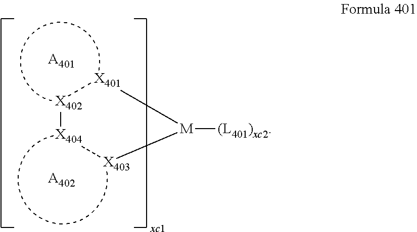

in Formula 401 may be identical to or different from one another. When xc1 in Formula 401 is two or more, A401 and A402 of one ligand may each independently be respectively connected to A401 and A402 of other neighboring ligands, either directly (e.g., via a bond such as a single bond) or via a linker (e.g., a C1-C5 alkylene group, —N(R′)— (wherein R′ may be a C1-C10 alkyl group or a C6-C20 aryl group) and/or —C(═O)—) therebetween.


Ar601-[(L601)xe1-E601]xe2. Formula 601


| TABLE 1 | ||||
| Hole transport region | Driving | Lumi- | Effi- | |
| hole auxiliary | hole transport | voltage | nance | ciency | |
| layer | layer | (V) | (cd/m2) | (cd/A) | |
| Example 1 | Compound 1 | Compound 105 | 3.7 | 805 | 7.5 |
| Example 2 | Compound 4 | Compound 105 | 3.9. | 722 | 7.6 |
| Example 3 | Compound 7 | Compound 105 | 4.0 | 829 | 8.1 |
| Example 4 | Compound 9 | Compound 105 | 4.3 | 642 | 6.1 |
| Comparative | Compound 1 | TPD | 5.0 | 324 | 4.8 |
| Example 1 | |||||
| Comparative | NPB | Compound 105 | 4.8 | 213 | 3.7. |
| Example 2 | |||||
| Comparative | Compound 4 | TPD | 4.6 | 426 | 5.1 |
| Example 3 | |||||
| Comparative | NPB | TPD | 4.7 | 457 | 4.8 |
| Example 4 | |||||
| Compound 105 | |||||
 |
|||||
 |
|||||
 |
|||||
 |
|||||
 |
|||||
 |
|||||
 |
|||||
Claims (2)


Applications Claiming Priority (4)
| Application Number | Priority Date | Filing Date | Title |
|---|---|---|---|
| KR10-2015-0062011 | 2015-04-30 | ||
| KR20150062011 | 2015-04-30 | ||
| KR1020160029700A KR20160130150A (en) | 2015-04-30 | 2016-03-11 | Organic light emitting device |
| KR10-2016-0029700 | 2016-03-11 |
Publications (2)
| Publication Number | Publication Date |
|---|---|
| US20160322579A1 US20160322579A1 (en) | 2016-11-03 |
| US10862043B2 true US10862043B2 (en) | 2020-12-08 |
Family
ID=57205333
Family Applications (1)
| Application Number | Title | Priority Date | Filing Date |
|---|---|---|---|
| US15/140,417 Active 2037-05-05 US10862043B2 (en) | 2015-04-30 | 2016-04-27 | Organic light-emitting device |
Country Status (1)
| Country | Link |
|---|---|
| US (1) | US10862043B2 (en) |
Families Citing this family (1)
| Publication number | Priority date | Publication date | Assignee | Title |
|---|---|---|---|---|
| KR102349284B1 (en) * | 2014-12-30 | 2022-01-11 | 삼성디스플레이 주식회사 | Amine-based compound and organic light emitting device comprising the same |
Citations (8)
| Publication number | Priority date | Publication date | Assignee | Title |
|---|---|---|---|---|
| EP2447250A1 (en) | 2010-10-26 | 2012-05-02 | Samsung Mobile Display Co., Ltd. | Organic light-emitting device |
| US20130119355A1 (en) | 2011-11-10 | 2013-05-16 | Samsung Display Co., Ltd. | Styryl-based compound, composition containing styryl-based compound, and organic light emitting diode including styryl-based compound |
| KR20130105192A (en) | 2012-03-16 | 2013-09-25 | 단국대학교 산학협력단 | Aromatic amine compound and organic electroluminescent device including the same |
| KR20140034183A (en) | 2011-05-13 | 2014-03-19 | 이데미쓰 고산 가부시키가이샤 | Organic el multi-color light-emitting device |
| KR20140087882A (en) | 2012-12-31 | 2014-07-09 | 제일모직주식회사 | COMPOUND FOR ORGANIC OPTOELECTRONIC DEVICE, ORGANIC LiGHT EMITTING DIODE INCLUDING THE SAME AND DISPLAY INCLUDING THE ORGANIC LiGHT EMITTING DIODE |
| US20160163994A1 (en) * | 2013-08-05 | 2016-06-09 | Duk San Neolux Co., Ltd. | Organic electronic element comprising compound for organic electronic element, and electronic device thereof |
| WO2016105138A2 (en) * | 2014-12-26 | 2016-06-30 | 주식회사 두산 | Organic compound and organo-electroluminescent device including same |
| US20170244047A1 (en) * | 2014-08-29 | 2017-08-24 | Duk San Neolux Co., Ltd. | Compound for organic electronic element, organic electronic element using the same, and an electronic device |
-
2016
- 2016-04-27 US US15/140,417 patent/US10862043B2/en active Active
Patent Citations (11)
| Publication number | Priority date | Publication date | Assignee | Title |
|---|---|---|---|---|
| EP2447250A1 (en) | 2010-10-26 | 2012-05-02 | Samsung Mobile Display Co., Ltd. | Organic light-emitting device |
| KR20120043623A (en) | 2010-10-26 | 2012-05-04 | 삼성모바일디스플레이주식회사 | Organic light emitting device |
| KR20140034183A (en) | 2011-05-13 | 2014-03-19 | 이데미쓰 고산 가부시키가이샤 | Organic el multi-color light-emitting device |
| US20140159023A1 (en) | 2011-05-13 | 2014-06-12 | Idemitsu Co., Ltd. | Organic el multi-color light-emitting device |
| US20130119355A1 (en) | 2011-11-10 | 2013-05-16 | Samsung Display Co., Ltd. | Styryl-based compound, composition containing styryl-based compound, and organic light emitting diode including styryl-based compound |
| KR20130051807A (en) | 2011-11-10 | 2013-05-21 | 삼성디스플레이 주식회사 | Styrly-based compound, composition containding the styryl-based compound and organic light emitting diode comprising the same |
| KR20130105192A (en) | 2012-03-16 | 2013-09-25 | 단국대학교 산학협력단 | Aromatic amine compound and organic electroluminescent device including the same |
| KR20140087882A (en) | 2012-12-31 | 2014-07-09 | 제일모직주식회사 | COMPOUND FOR ORGANIC OPTOELECTRONIC DEVICE, ORGANIC LiGHT EMITTING DIODE INCLUDING THE SAME AND DISPLAY INCLUDING THE ORGANIC LiGHT EMITTING DIODE |
| US20160163994A1 (en) * | 2013-08-05 | 2016-06-09 | Duk San Neolux Co., Ltd. | Organic electronic element comprising compound for organic electronic element, and electronic device thereof |
| US20170244047A1 (en) * | 2014-08-29 | 2017-08-24 | Duk San Neolux Co., Ltd. | Compound for organic electronic element, organic electronic element using the same, and an electronic device |
| WO2016105138A2 (en) * | 2014-12-26 | 2016-06-30 | 주식회사 두산 | Organic compound and organo-electroluminescent device including same |
Non-Patent Citations (1)
| Title |
|---|
| WO2016105138A2, Machine Transition, Jun. 2012. * |
Also Published As
| Publication number | Publication date |
|---|---|
| US20160322579A1 (en) | 2016-11-03 |
Similar Documents
| Publication | Publication Date | Title |
|---|---|---|
| US10665789B2 (en) | Organic light-emitting device | |
| US9172046B1 (en) | Organic light-emitting device | |
| US9972789B2 (en) | Organic light-emitting device | |
| US10333074B2 (en) | Organic light-emitting device | |
| US10038144B2 (en) | Organic light emitting device | |
| US9401484B2 (en) | Organic light-emitting device having increased electron transport ability of an electron transport region | |
| US20170117486A1 (en) | Organic light-emitting device | |
| US20170125697A1 (en) | Organic light-emitting device | |
| US9917262B2 (en) | Organic light-emitting device | |
| US10727417B2 (en) | Organic light-emitting device | |
| US10978643B2 (en) | Organic light-emitting device | |
| US20160028014A1 (en) | Organic light-emitting device | |
| US10825993B2 (en) | Organic light-emitting device and method of manufacturing the same | |
| US9859503B2 (en) | Organic light-emitting device | |
| US11322705B2 (en) | Organic light-emitting device | |
| US9825107B2 (en) | Organic light-emitting device | |
| US11944003B2 (en) | Organic light-emitting device | |
| US11038113B2 (en) | Organic light-emitting device | |
| US20170133599A1 (en) | Organic light-emitting device | |
| US10186666B2 (en) | Condensed-cyclic compound and organic light emitting device including the same | |
| US11653563B2 (en) | Organic light-emitting device | |
| US10032994B2 (en) | Organic light-emitting device | |
| US20170125690A1 (en) | Organic light-emitting device | |
| US20170155054A1 (en) | Organic light-emitting device | |
| US10862043B2 (en) | Organic light-emitting device |
Legal Events
| Date | Code | Title | Description |
|---|---|---|---|
| AS | Assignment |
Owner name: SAMSUNG DISPLAY CO., LTD., KOREA, REPUBLIC OF Free format text: ASSIGNMENT OF ASSIGNORS INTEREST;ASSIGNORS:HWANG, JINSOO;YOON, SEOKGYU;JEONG, HYEIN;REEL/FRAME:038446/0405 Effective date: 20160426 |
|
| STPP | Information on status: patent application and granting procedure in general |
Free format text: DOCKETED NEW CASE - READY FOR EXAMINATION |
|
| STPP | Information on status: patent application and granting procedure in general |
Free format text: NON FINAL ACTION MAILED |
|
| STPP | Information on status: patent application and granting procedure in general |
Free format text: FINAL REJECTION MAILED |
|
| STPP | Information on status: patent application and granting procedure in general |
Free format text: RESPONSE AFTER FINAL ACTION FORWARDED TO EXAMINER |
|
| STPP | Information on status: patent application and granting procedure in general |
Free format text: ADVISORY ACTION MAILED |
|
| STPP | Information on status: patent application and granting procedure in general |
Free format text: DOCKETED NEW CASE - READY FOR EXAMINATION |
|
| STPP | Information on status: patent application and granting procedure in general |
Free format text: NON FINAL ACTION MAILED |
|
| STPP | Information on status: patent application and granting procedure in general |
Free format text: RESPONSE TO NON-FINAL OFFICE ACTION ENTERED AND FORWARDED TO EXAMINER |
|
| STCF | Information on status: patent grant |
Free format text: PATENTED CASE |