US10861802B2 - Method for forming at least one electrical discontinuity in an integrated circuit, and corresponding integrated circuit - Google Patents
Method for forming at least one electrical discontinuity in an integrated circuit, and corresponding integrated circuit Download PDFInfo
- Publication number
- US10861802B2 US10861802B2 US16/208,253 US201816208253A US10861802B2 US 10861802 B2 US10861802 B2 US 10861802B2 US 201816208253 A US201816208253 A US 201816208253A US 10861802 B2 US10861802 B2 US 10861802B2
- Authority
- US
- United States
- Prior art keywords
- pad
- source
- electrically conductive
- conductive pads
- insulating
- Prior art date
- Legal status (The legal status is an assumption and is not a legal conclusion. Google has not performed a legal analysis and makes no representation as to the accuracy of the status listed.)
- Active
Links
Images


Classifications
-
- H01L23/573—
-
- H—ELECTRICITY
- H10—SEMICONDUCTOR DEVICES; ELECTRIC SOLID-STATE DEVICES NOT OTHERWISE PROVIDED FOR
- H10W—GENERIC PACKAGES, INTERCONNECTIONS, CONNECTORS OR OTHER CONSTRUCTIONAL DETAILS OF DEVICES COVERED BY CLASS H10
- H10W42/00—Arrangements for protection of devices
- H10W42/40—Arrangements for protection of devices protecting against tampering, e.g. unauthorised inspection or reverse engineering
-
- H—ELECTRICITY
- H10—SEMICONDUCTOR DEVICES; ELECTRIC SOLID-STATE DEVICES NOT OTHERWISE PROVIDED FOR
- H10W—GENERIC PACKAGES, INTERCONNECTIONS, CONNECTORS OR OTHER CONSTRUCTIONAL DETAILS OF DEVICES COVERED BY CLASS H10
- H10W99/00—Subject matter not provided for in other groups of this subclass
-
- H01L21/31111—
-
- H01L21/768—
-
- H01L21/76816—
-
- H01L21/823475—
-
- H01L23/522—
-
- H01L23/5226—
-
- H01L23/5283—
-
- H01L23/585—
-
- H01L24/03—
-
- H01L24/06—
-
- H01L27/088—
-
- H—ELECTRICITY
- H10—SEMICONDUCTOR DEVICES; ELECTRIC SOLID-STATE DEVICES NOT OTHERWISE PROVIDED FOR
- H10D—INORGANIC ELECTRIC SEMICONDUCTOR DEVICES
- H10D84/00—Integrated devices formed in or on semiconductor substrates that comprise only semiconducting layers, e.g. on Si wafers or on GaAs-on-Si wafers
- H10D84/01—Manufacture or treatment
- H10D84/0123—Integrating together multiple components covered by H10D12/00 or H10D30/00, e.g. integrating multiple IGBTs
- H10D84/0126—Integrating together multiple components covered by H10D12/00 or H10D30/00, e.g. integrating multiple IGBTs the components including insulated gates, e.g. IGFETs
- H10D84/0149—Manufacturing their interconnections or electrodes, e.g. source or drain electrodes
-
- H—ELECTRICITY
- H10—SEMICONDUCTOR DEVICES; ELECTRIC SOLID-STATE DEVICES NOT OTHERWISE PROVIDED FOR
- H10D—INORGANIC ELECTRIC SEMICONDUCTOR DEVICES
- H10D84/00—Integrated devices formed in or on semiconductor substrates that comprise only semiconducting layers, e.g. on Si wafers or on GaAs-on-Si wafers
- H10D84/01—Manufacture or treatment
- H10D84/02—Manufacture or treatment characterised by using material-based technologies
- H10D84/03—Manufacture or treatment characterised by using material-based technologies using Group IV technology, e.g. silicon technology or silicon-carbide [SiC] technology
- H10D84/038—Manufacture or treatment characterised by using material-based technologies using Group IV technology, e.g. silicon technology or silicon-carbide [SiC] technology using silicon technology, e.g. SiGe
-
- H—ELECTRICITY
- H10—SEMICONDUCTOR DEVICES; ELECTRIC SOLID-STATE DEVICES NOT OTHERWISE PROVIDED FOR
- H10D—INORGANIC ELECTRIC SEMICONDUCTOR DEVICES
- H10D84/00—Integrated devices formed in or on semiconductor substrates that comprise only semiconducting layers, e.g. on Si wafers or on GaAs-on-Si wafers
- H10D84/80—Integrated devices formed in or on semiconductor substrates that comprise only semiconducting layers, e.g. on Si wafers or on GaAs-on-Si wafers characterised by the integration of at least one component covered by groups H10D12/00 or H10D30/00, e.g. integration of IGFETs
- H10D84/82—Integrated devices formed in or on semiconductor substrates that comprise only semiconducting layers, e.g. on Si wafers or on GaAs-on-Si wafers characterised by the integration of at least one component covered by groups H10D12/00 or H10D30/00, e.g. integration of IGFETs of only field-effect components
- H10D84/83—Integrated devices formed in or on semiconductor substrates that comprise only semiconducting layers, e.g. on Si wafers or on GaAs-on-Si wafers characterised by the integration of at least one component covered by groups H10D12/00 or H10D30/00, e.g. integration of IGFETs of only field-effect components of only insulated-gate FETs [IGFET]
- H10D84/8312—Integrated devices formed in or on semiconductor substrates that comprise only semiconducting layers, e.g. on Si wafers or on GaAs-on-Si wafers characterised by the integration of at least one component covered by groups H10D12/00 or H10D30/00, e.g. integration of IGFETs of only field-effect components of only insulated-gate FETs [IGFET] the IGFETs characterised by having different source or drain region structures, e.g. IGFETs having symmetrical source or drain regions integrated with IGFETs having asymmetrical source or drain regions
-
- H—ELECTRICITY
- H10—SEMICONDUCTOR DEVICES; ELECTRIC SOLID-STATE DEVICES NOT OTHERWISE PROVIDED FOR
- H10P—GENERIC PROCESSES OR APPARATUS FOR THE MANUFACTURE OR TREATMENT OF DEVICES COVERED BY CLASS H10
- H10P50/00—Etching of wafers, substrates or parts of devices
- H10P50/20—Dry etching; Plasma etching; Reactive-ion etching
- H10P50/28—Dry etching; Plasma etching; Reactive-ion etching of insulating materials
- H10P50/282—Dry etching; Plasma etching; Reactive-ion etching of insulating materials of inorganic materials
- H10P50/283—Dry etching; Plasma etching; Reactive-ion etching of insulating materials of inorganic materials by chemical means
-
- H—ELECTRICITY
- H10—SEMICONDUCTOR DEVICES; ELECTRIC SOLID-STATE DEVICES NOT OTHERWISE PROVIDED FOR
- H10W—GENERIC PACKAGES, INTERCONNECTIONS, CONNECTORS OR OTHER CONSTRUCTIONAL DETAILS OF DEVICES COVERED BY CLASS H10
- H10W20/00—Interconnections in chips, wafers or substrates
- H10W20/01—Manufacture or treatment
- H10W20/071—Manufacture or treatment of dielectric parts thereof
- H10W20/081—Manufacture or treatment of dielectric parts thereof by forming openings in the dielectric parts
- H10W20/089—Manufacture or treatment of dielectric parts thereof by forming openings in the dielectric parts using processes for implementing desired shapes or dispositions of the openings, e.g. double patterning
-
- H—ELECTRICITY
- H10—SEMICONDUCTOR DEVICES; ELECTRIC SOLID-STATE DEVICES NOT OTHERWISE PROVIDED FOR
- H10W—GENERIC PACKAGES, INTERCONNECTIONS, CONNECTORS OR OTHER CONSTRUCTIONAL DETAILS OF DEVICES COVERED BY CLASS H10
- H10W20/00—Interconnections in chips, wafers or substrates
- H10W20/40—Interconnections external to wafers or substrates, e.g. back-end-of-line [BEOL] metallisations or vias connecting to gate electrodes
- H10W20/41—Interconnections external to wafers or substrates, e.g. back-end-of-line [BEOL] metallisations or vias connecting to gate electrodes characterised by their conductive parts
- H10W20/42—Vias, e.g. via plugs
-
- H—ELECTRICITY
- H10—SEMICONDUCTOR DEVICES; ELECTRIC SOLID-STATE DEVICES NOT OTHERWISE PROVIDED FOR
- H10W—GENERIC PACKAGES, INTERCONNECTIONS, CONNECTORS OR OTHER CONSTRUCTIONAL DETAILS OF DEVICES COVERED BY CLASS H10
- H10W20/00—Interconnections in chips, wafers or substrates
- H10W20/40—Interconnections external to wafers or substrates, e.g. back-end-of-line [BEOL] metallisations or vias connecting to gate electrodes
- H10W20/41—Interconnections external to wafers or substrates, e.g. back-end-of-line [BEOL] metallisations or vias connecting to gate electrodes characterised by their conductive parts
- H10W20/435—Cross-sectional shapes or dispositions of interconnections
-
- H—ELECTRICITY
- H10—SEMICONDUCTOR DEVICES; ELECTRIC SOLID-STATE DEVICES NOT OTHERWISE PROVIDED FOR
- H10W—GENERIC PACKAGES, INTERCONNECTIONS, CONNECTORS OR OTHER CONSTRUCTIONAL DETAILS OF DEVICES COVERED BY CLASS H10
- H10W42/00—Arrangements for protection of devices
-
- H—ELECTRICITY
- H10—SEMICONDUCTOR DEVICES; ELECTRIC SOLID-STATE DEVICES NOT OTHERWISE PROVIDED FOR
- H10W—GENERIC PACKAGES, INTERCONNECTIONS, CONNECTORS OR OTHER CONSTRUCTIONAL DETAILS OF DEVICES COVERED BY CLASS H10
- H10W72/00—Interconnections or connectors in packages
- H10W72/01—Manufacture or treatment
- H10W72/019—Manufacture or treatment of bond pads
-
- H—ELECTRICITY
- H10—SEMICONDUCTOR DEVICES; ELECTRIC SOLID-STATE DEVICES NOT OTHERWISE PROVIDED FOR
- H10W—GENERIC PACKAGES, INTERCONNECTIONS, CONNECTORS OR OTHER CONSTRUCTIONAL DETAILS OF DEVICES COVERED BY CLASS H10
- H10W72/00—Interconnections or connectors in packages
- H10W72/20—Bump connectors, e.g. solder bumps or copper pillars; Dummy bumps; Thermal bumps
-
- H—ELECTRICITY
- H10—SEMICONDUCTOR DEVICES; ELECTRIC SOLID-STATE DEVICES NOT OTHERWISE PROVIDED FOR
- H10W—GENERIC PACKAGES, INTERCONNECTIONS, CONNECTORS OR OTHER CONSTRUCTIONAL DETAILS OF DEVICES COVERED BY CLASS H10
- H10W72/00—Interconnections or connectors in packages
- H10W72/90—Bond pads, in general
-
- H01L21/76802—
-
- H—ELECTRICITY
- H10—SEMICONDUCTOR DEVICES; ELECTRIC SOLID-STATE DEVICES NOT OTHERWISE PROVIDED FOR
- H10D—INORGANIC ELECTRIC SEMICONDUCTOR DEVICES
- H10D84/00—Integrated devices formed in or on semiconductor substrates that comprise only semiconducting layers, e.g. on Si wafers or on GaAs-on-Si wafers
- H10D84/80—Integrated devices formed in or on semiconductor substrates that comprise only semiconducting layers, e.g. on Si wafers or on GaAs-on-Si wafers characterised by the integration of at least one component covered by groups H10D12/00 or H10D30/00, e.g. integration of IGFETs
- H10D84/82—Integrated devices formed in or on semiconductor substrates that comprise only semiconducting layers, e.g. on Si wafers or on GaAs-on-Si wafers characterised by the integration of at least one component covered by groups H10D12/00 or H10D30/00, e.g. integration of IGFETs of only field-effect components
- H10D84/83—Integrated devices formed in or on semiconductor substrates that comprise only semiconducting layers, e.g. on Si wafers or on GaAs-on-Si wafers characterised by the integration of at least one component covered by groups H10D12/00 or H10D30/00, e.g. integration of IGFETs of only field-effect components of only insulated-gate FETs [IGFET]
- H10D84/83125—Integrated devices formed in or on semiconductor substrates that comprise only semiconducting layers, e.g. on Si wafers or on GaAs-on-Si wafers characterised by the integration of at least one component covered by groups H10D12/00 or H10D30/00, e.g. integration of IGFETs of only field-effect components of only insulated-gate FETs [IGFET] the IGFETs characterised by having shared source or drain regions
-
- H—ELECTRICITY
- H10—SEMICONDUCTOR DEVICES; ELECTRIC SOLID-STATE DEVICES NOT OTHERWISE PROVIDED FOR
- H10W—GENERIC PACKAGES, INTERCONNECTIONS, CONNECTORS OR OTHER CONSTRUCTIONAL DETAILS OF DEVICES COVERED BY CLASS H10
- H10W20/00—Interconnections in chips, wafers or substrates
- H10W20/01—Manufacture or treatment
- H10W20/071—Manufacture or treatment of dielectric parts thereof
- H10W20/081—Manufacture or treatment of dielectric parts thereof by forming openings in the dielectric parts
Definitions
- Modes of implementation and embodiments relate to integrated circuits, and more particularly to the protection thereof from reverse engineering carried out on the basis of photographic top views of various layers of the integrated circuit.
- a method for forming at least one electrical discontinuity in an integrated circuit comprising the production, above a semiconductor substrate, of a multitude of electrically conductive pads (contacts) situated between component zones of the integrated circuit and a first metallization level of the integrated circuit, respectively, and encapsulated in an insulating region, said multitude of pads including first pads, in electrical contact with corresponding first component zones, and at least one second pad, not in electrical contact with a corresponding second component zone, so as to form said at least one electrical discontinuity.
- said production comprises:
- the insulating layer that lines the orifice and the second component zone have a composition identical to that of a part of the insulating region will make it particularly difficult to discriminate between a second pad and a first pad.
- the insulating region may include a first insulating layer, for example of silicon carbon nitride (SiCN), covered with a second insulating layer, for example of tetraethyl orthosilicate (TEOS), or else a material having a low dielectric constant, such as SiO 2 or even SiOC.
- This second insulating layer is, for example, better known as the PMD (pre-metal dielectric) layer by those skilled in the art.
- the insulating layer that lines the internal wall of the orifice and the second component zone may also be formed of a material having a composition identical to that of the material of the second insulating layer.
- the filling of the lined orifice with a filler material having a composition identical to that of the first pads also makes it difficult to discriminate between a first pad and a second pad.
- This filler material may comprise tungsten, for example.
- said localized etching and said lining are configured to make said at least one lined orifice such that its aperture size leads, after filling thereof, to said at least one second pad having a cross section of a size analogous to that of the cross section of each first pad.
- the orifice prior to lining, is slightly larger than the orifice used to form the first pads, and this size and the thickness of the lining layer are chosen so as ultimately to obtain a contact (pad) size that is analogous for all of the pads, whether these pads be first pads or second pads.
- analogous is here understood to mean identical or substantially identical, to within manufacturing tolerances.
- Said at least one second component zone may comprise an active region of a transistor, for example the drain region. That being said, this example is in no way restrictive, and any component zone may be envisioned, such as, for example, a polysilicon line, for forming said electrical discontinuity.
- an integrated circuit comprising, above a semiconductor substrate, a multitude of electrically conductive pads situated between component zones of the integrated circuit and a first metallization level of the integrated circuit, respectively, and encapsulated in an insulating region, said multitude of pads including first pads, in electrical contact with corresponding first component zones, and at least one second pad, not in electrical contact with a corresponding second component zone, so as to form at least one electrical discontinuity.
- said at least one second pad is completely embedded in said insulating region, a part of said insulating region being situated between said at least one second component zone and a bottom end of said at least one second pad.
- said at least one second pad has a cross section of a size analogous to that of the cross section of each first pad.
- an object for example a chip card or an electronic appliance, such as for example a cellular mobile telephone or a tablet, including an integrated circuit such as defined hereinabove.
- FIG. 1 illustrates an example of an integrated circuit from the prior art
- FIGS. 2 to 9 schematically illustrate an example of a method according to the invention and an example of an integrated circuit
- FIG. 10 schematically illustrates a chip card.
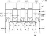
- the reference IC 1 denotes an example of an integrated circuit from the prior art.
- This integrated circuit IC 1 includes, in a conventional manner, a semiconductor substrate SB, as well as insulating regions RIS 1 , for example shallow trench isolations (STIs) that bound a substrate region inside of which are, for example, formed active component zones Z 1 .
- STIs shallow trench isolations
- These components here include, for example, transistors TR, the zones Z 1 then forming source or drain regions of these transistors.
- the components of the integrated circuit are separated from the first metallization level M 1 by an insulating region RIS 2 including, here, a first insulating layer CS 1 , for example made of SiCN, surmounted by a second insulating layer CS 2 , for example made of a material such as SiO 2 .
- the component zones Z 1 are connected to metal tracks PST of the first metallization level M 1 by first pads PLT 1 , commonly referred to as contacts by those skilled in the art. These pads PLT 1 are electrically conductive, for example made of tungsten, and are encapsulated in the insulating region RIS 2 .
- FIGS. 2 to 9 in order to describe an example of a manufacturing method making it possible to create at least one electrical discontinuity in the integrated circuit.
- the integrated circuit IC 2 has been shown at a manufacturing stage in which the various components, here including, for example, MOS transistors TR 0 , TR 1 and TR 2 , have been produced in a manner that is conventional and known per se and then subsequently encapsulated in the insulating region RIS 2 , including the first insulating layer CS 1 , for example made of SiCN, surmounted by the second insulating layer CS 2 , for example of SiO 2 , also known as the pre-metal dielectric by those skilled in the art.
- the various components here including, for example, MOS transistors TR 0 , TR 1 and TR 2 , have been produced in a manner that is conventional and known per se and then subsequently encapsulated in the insulating region RIS 2 , including the first insulating layer CS 1 , for example made of SiCN, surmounted by the second insulating layer CS 2 , for example of SiO 2 , also known as the pre-metal dielectric by those skilled in the art.
- first component zones Z 1 and a second component zone Z 2 there is a differentiation between first component zones Z 1 and a second component zone Z 2 .
- the first pads PLT 1 encapsulated in the insulating region RIS 2 are formed.
- These first pads PLT 1 make contact with the first component zones Z 1 by way, as is conventional, of silicided parts of these zones Z 1 .
- first pads PLT 1 have been produced in a manner that is conventional and known per se by initial localized etching of the insulating region RIS 2 using a first mask MSK 1 ( FIG. 3 ) that delineates the locations (mask openings) EMP 1 of the orifices intended to be etched into the insulating layer RIS 2 in order to subsequently be filled with a filler material, for example tungsten, so as to form the pads PLT 1 .
- MSK 1 FIG. 3
- this mask MSK 1 does not include the location of the future second pad, which will be situated facing the second component zone Z 2 .
- a second localized etching of the insulating region RIS 2 is carried out above the second component zone Z 2 so as to form an orifice OR 1 leading to this second component zone Z 2 .
- This second localized etching is carried out using a second mask MSK 2 ( FIG. 5 ) that this time delineates the location (mask opening) EMP 2 of the orifice OR 1 .
- a cross-sectional area of the mask opening EMP 2 is larger than a cross-sectional area of the mask opening EMP 1 .
- the size of a cross section of the orifice OR 1 is larger than the size of a cross section of a pad PLT 1 (and its corresponding opening that was filled with metal material).
- this orifice OR 1 it is preferable to enlarge this orifice OR 1 so as to ultimately obtain, as will be seen in more detail hereinafter, a second pad (contact) above this zone Z 2 , the size of the cross section of which is analogous, that is to say identical or substantially identical, to within a manufacturing tolerance, to the size of a cross section of a first pad PLT 1 .
- the internal wall of the orifice OR 1 , as well as the component zone Z 2 are lined with an insulating layer CS 3 advantageously having a composition identical to that of the second insulating layer CS 2 .
- the insulating layer CS 3 may be a deposited SiO 2 layer to match the material used for the second insulating layer CS 2 . Any suitable process for a conformal layer or lining deposit of insulating material may be used.
- the size of the orifice OR 1 and the thickness of the insulating layer CS 3 are chosen such that the size D 2 of a cross section of the thus-lined orifice OR 2 is analogous to the size D 1 of a cross section of a first pad PLT 1 .
- the lined orifice OR 2 is filled, in a manner that is conventional and known per se, with a filler material identical to that forming the pads PLT 1 , thereby making it possible to obtain a second pad PLT 2 having a composition analogous to that of the pads PLT 1 and having a cross-section size D 2 analogous to the size D 1 of the cross section of a pad PLT 1 .
- the bottom end of the second pad PLT 2 is located a distance away from the second component zone Z 2 and is separated therefrom by the insulating layer CS 3 . Consequently, the second pad PLT 2 is not in electrical contact with the zone Z 2 , thus creating an electrical discontinuity in the integrated circuit.
- the second component zone Z 2 is the drain of the transistor TR 0 , this transistor TR 0 will be permanently electrically OFF, whereas, seen from above, it appears to be a conventional transistor.
- the first metallization level M 1 including the metal tracks PST encapsulated in an inter-track dielectric, is produced in a manner that is conventional and known per se.
- the method for manufacturing the integrated circuit that is to say in particular the production of the upper metallization level, is subsequently continued in a conventional manner.
- the integrated circuit IC 2 includes a multitude of electrically conductive pads situated between component zones of the integrated circuit and the first metallization level M 1 , respectively, and encapsulated in the insulating region RIS 2 .
- This multitude of pads includes first pads PLT 1 , in electrical contact with corresponding first component zones Z 1 , and at least one second pad PLT 2 , not in electrical contact with a corresponding second component zone Z 2 , so as to form said at least one electrical discontinuity.
- the second pad PLT 2 is completely embedded in the insulating region RIS 2 , a part of the insulating region, in the present case the layer CS 3 , being situated between the second component zone Z 2 and a bottom end of this second pad PLT 2 .
- this second pad PLT 2 advantageously has a cross section of a size analogous to that of the cross section of each first pad, and a composition analogous to that of the first pads.
- Such an integrated circuit IC 2 may be incorporated into any object, in particular a chip card CP as illustrated very schematically in FIG. 10 .
Landscapes
- Internal Circuitry In Semiconductor Integrated Circuit Devices (AREA)
- Chemical & Material Sciences (AREA)
- Chemical Kinetics & Catalysis (AREA)
- General Chemical & Material Sciences (AREA)
- Engineering & Computer Science (AREA)
- Manufacturing & Machinery (AREA)
- Semiconductor Integrated Circuits (AREA)
Abstract
Description
-
- initial production of the first pads encapsulated in said insulating region,
- localized etching of said insulating region at the location of said at least one second pad, so as to form at least one orifice leading to said corresponding second component zone,
- lining the internal wall of said at least one orifice and said second component zone with an insulating layer having a composition identical to that of at least one part of said insulating region, and
- filling said at least one lined orifice with a filler material having a composition identical to that of the first pads, so as to form said at least one second pad.
Claims (17)
Priority Applications (1)
| Application Number | Priority Date | Filing Date | Title |
|---|---|---|---|
| US16/208,253 US10861802B2 (en) | 2016-11-22 | 2018-12-03 | Method for forming at least one electrical discontinuity in an integrated circuit, and corresponding integrated circuit |
Applications Claiming Priority (4)
| Application Number | Priority Date | Filing Date | Title |
|---|---|---|---|
| FR1661347 | 2016-11-22 | ||
| FR1661347A FR3059145B1 (en) | 2016-11-22 | 2016-11-22 | METHOD OF FORMING AT LEAST ONE ELECTRICAL DISCONTINUITY IN AN INTEGRATED CIRCUIT AND CORRESPONDING INTEGRATED CIRCUIT |
| US15/596,767 US10177101B2 (en) | 2016-11-22 | 2017-05-16 | Method for forming at least one electrical discontinuity in an integrated circuit, and corresponding integrated circuit |
| US16/208,253 US10861802B2 (en) | 2016-11-22 | 2018-12-03 | Method for forming at least one electrical discontinuity in an integrated circuit, and corresponding integrated circuit |
Related Parent Applications (1)
| Application Number | Title | Priority Date | Filing Date |
|---|---|---|---|
| US15/596,767 Division US10177101B2 (en) | 2016-11-22 | 2017-05-16 | Method for forming at least one electrical discontinuity in an integrated circuit, and corresponding integrated circuit |
Publications (2)
| Publication Number | Publication Date |
|---|---|
| US20190103369A1 US20190103369A1 (en) | 2019-04-04 |
| US10861802B2 true US10861802B2 (en) | 2020-12-08 |
Family
ID=59152932
Family Applications (2)
| Application Number | Title | Priority Date | Filing Date |
|---|---|---|---|
| US15/596,767 Active US10177101B2 (en) | 2016-11-22 | 2017-05-16 | Method for forming at least one electrical discontinuity in an integrated circuit, and corresponding integrated circuit |
| US16/208,253 Active US10861802B2 (en) | 2016-11-22 | 2018-12-03 | Method for forming at least one electrical discontinuity in an integrated circuit, and corresponding integrated circuit |
Family Applications Before (1)
| Application Number | Title | Priority Date | Filing Date |
|---|---|---|---|
| US15/596,767 Active US10177101B2 (en) | 2016-11-22 | 2017-05-16 | Method for forming at least one electrical discontinuity in an integrated circuit, and corresponding integrated circuit |
Country Status (3)
| Country | Link |
|---|---|
| US (2) | US10177101B2 (en) |
| CN (2) | CN108091576A (en) |
| FR (1) | FR3059145B1 (en) |
Families Citing this family (1)
| Publication number | Priority date | Publication date | Assignee | Title |
|---|---|---|---|---|
| FR3059145B1 (en) | 2016-11-22 | 2019-07-19 | Stmicroelectronics (Rousset) Sas | METHOD OF FORMING AT LEAST ONE ELECTRICAL DISCONTINUITY IN AN INTEGRATED CIRCUIT AND CORRESPONDING INTEGRATED CIRCUIT |
Citations (13)
| Publication number | Priority date | Publication date | Assignee | Title |
|---|---|---|---|---|
| JPS61147551A (en) | 1984-12-21 | 1986-07-05 | Nec Corp | Semiconductor device |
| WO1998057373A1 (en) | 1997-06-13 | 1998-12-17 | Inside Technologies | Method for making an integrated circuit and integrated circuit produced by said method |
| US6791191B2 (en) | 2001-01-24 | 2004-09-14 | Hrl Laboratories, Llc | Integrated circuits protected against reverse engineering and method for fabricating the same using vias without metal terminations |
| US7402514B2 (en) | 2003-01-24 | 2008-07-22 | Texas Instruments Incorporated | Line-to-line reliability enhancement using a dielectric liner for a low dielectric constant interlevel and intralevel (or intermetal and intrametal) dielectric layer |
| US20080174022A1 (en) | 2007-01-22 | 2008-07-24 | Taiwan Semiconductor Manufacturing Co., Ltd. | Semiconductor device and fabrication method thereof |
| JP2008205019A (en) | 2007-02-16 | 2008-09-04 | Toshiba Corp | Semiconductor integrated circuit and manufacturing method thereof |
| US20080293242A1 (en) | 2002-07-01 | 2008-11-27 | International Business Machiness Corporation | Metal spacer in single and dual damascene processing |
| US20090111257A1 (en) | 2007-10-26 | 2009-04-30 | International Business Machines Corporation | Techniques for Impeding Reverse Engineering |
| US20100155846A1 (en) * | 2008-12-19 | 2010-06-24 | Niloy Mukherjee | Metal-insulator-semiconductor tunneling contacts |
| DE102013224060A1 (en) | 2013-11-26 | 2015-05-28 | Ihp Gmbh - Innovations For High Performance Microelectronics / Leibniz-Institut Für Innovative Mikroelektronik | Complicating optical reverse engineering |
| US20160254227A1 (en) | 2015-02-26 | 2016-09-01 | International Business Machines Corporation | Semiconductor device security |
| US9502405B1 (en) * | 2015-08-27 | 2016-11-22 | International Business Machines Corporation | Semiconductor device with authentication code |
| CN207338359U (en) | 2016-11-22 | 2018-05-08 | 意法半导体(鲁塞)公司 | Integrated circuit and object |
Family Cites Families (1)
| Publication number | Priority date | Publication date | Assignee | Title |
|---|---|---|---|---|
| EP1193758A1 (en) * | 2000-10-02 | 2002-04-03 | STMicroelectronics S.r.l. | Anti-deciphering contacts |
-
2016
- 2016-11-22 FR FR1661347A patent/FR3059145B1/en active Active
-
2017
- 2017-05-16 US US15/596,767 patent/US10177101B2/en active Active
- 2017-05-18 CN CN201710351609.7A patent/CN108091576A/en active Pending
- 2017-05-18 CN CN201720557559.3U patent/CN207338359U/en active Active
-
2018
- 2018-12-03 US US16/208,253 patent/US10861802B2/en active Active
Patent Citations (15)
| Publication number | Priority date | Publication date | Assignee | Title |
|---|---|---|---|---|
| JPS61147551A (en) | 1984-12-21 | 1986-07-05 | Nec Corp | Semiconductor device |
| WO1998057373A1 (en) | 1997-06-13 | 1998-12-17 | Inside Technologies | Method for making an integrated circuit and integrated circuit produced by said method |
| DE69715472T2 (en) | 1997-06-13 | 2003-04-30 | Tomasz Kowalski | MANUFACTURING METHOD FOR AN INTEGRATED CIRCUIT AND THE INTEGRATED CIRCUIT PRODUCED BY IT |
| US6791191B2 (en) | 2001-01-24 | 2004-09-14 | Hrl Laboratories, Llc | Integrated circuits protected against reverse engineering and method for fabricating the same using vias without metal terminations |
| US20080293242A1 (en) | 2002-07-01 | 2008-11-27 | International Business Machiness Corporation | Metal spacer in single and dual damascene processing |
| US7402514B2 (en) | 2003-01-24 | 2008-07-22 | Texas Instruments Incorporated | Line-to-line reliability enhancement using a dielectric liner for a low dielectric constant interlevel and intralevel (or intermetal and intrametal) dielectric layer |
| US20080174022A1 (en) | 2007-01-22 | 2008-07-24 | Taiwan Semiconductor Manufacturing Co., Ltd. | Semiconductor device and fabrication method thereof |
| JP2008205019A (en) | 2007-02-16 | 2008-09-04 | Toshiba Corp | Semiconductor integrated circuit and manufacturing method thereof |
| US20090111257A1 (en) | 2007-10-26 | 2009-04-30 | International Business Machines Corporation | Techniques for Impeding Reverse Engineering |
| US20100155846A1 (en) * | 2008-12-19 | 2010-06-24 | Niloy Mukherjee | Metal-insulator-semiconductor tunneling contacts |
| CN102239546A (en) | 2008-12-19 | 2011-11-09 | 英特尔公司 | Metal-insulator-semiconductor tunneling contacts |
| DE102013224060A1 (en) | 2013-11-26 | 2015-05-28 | Ihp Gmbh - Innovations For High Performance Microelectronics / Leibniz-Institut Für Innovative Mikroelektronik | Complicating optical reverse engineering |
| US20160254227A1 (en) | 2015-02-26 | 2016-09-01 | International Business Machines Corporation | Semiconductor device security |
| US9502405B1 (en) * | 2015-08-27 | 2016-11-22 | International Business Machines Corporation | Semiconductor device with authentication code |
| CN207338359U (en) | 2016-11-22 | 2018-05-08 | 意法半导体(鲁塞)公司 | Integrated circuit and object |
Non-Patent Citations (2)
| Title |
|---|
| First Office Action and Search Report for co-pending CN Appl. No. 201710351609.7 dated Jul. 1, 2020 (8 pages). |
| INPI Search Report and Written Opinion for FR 1661347 dated Oct. 17, 2017 (7 pages). |
Also Published As
| Publication number | Publication date |
|---|---|
| CN207338359U (en) | 2018-05-08 |
| FR3059145B1 (en) | 2019-07-19 |
| US20180145040A1 (en) | 2018-05-24 |
| US10177101B2 (en) | 2019-01-08 |
| FR3059145A1 (en) | 2018-05-25 |
| CN108091576A (en) | 2018-05-29 |
| US20190103369A1 (en) | 2019-04-04 |
Similar Documents
| Publication | Publication Date | Title |
|---|---|---|
| US10199273B2 (en) | Method for forming semiconductor device with through silicon via | |
| US6686247B1 (en) | Self-aligned contacts to gates | |
| US20050236712A1 (en) | Substrate contact and method of forming the same | |
| US20150303108A1 (en) | Method for forming semiconductor device | |
| CN103515302B (en) | Semiconductor device and method of manufacture | |
| TW201411777A (en) | Method for reducing wettability of interconnect material at an angle interface and apparatus including the same | |
| US10861802B2 (en) | Method for forming at least one electrical discontinuity in an integrated circuit, and corresponding integrated circuit | |
| CN100420009C (en) | Semiconductor device and opening structure in semiconductor device | |
| US10903345B2 (en) | Power MOSFET with metal filled deep sinker contact for CSP | |
| US10269811B2 (en) | Selective SAC capping on fin field effect transistor structures and related methods | |
| US20060246726A1 (en) | Making contact with the emitter contact of a semiconductor | |
| US7666783B2 (en) | Method and arrangement for contacting terminals | |
| US10049982B2 (en) | Method for forming at least one electrical discontinuity in an interconnection part of an integrated circuit without addition of additional material, and corresponding integrated circuit | |
| TWI546866B (en) | Semiconductor device and fabricating method thereof | |
| US10049991B2 (en) | Method for forming at least one electrical discontinuity in an interconnection part of an integrated circuit, and corresponding integrated circuit | |
| JP4716870B2 (en) | Bipolar and CMOS integrated circuit structures with reduced contact height | |
| KR100887474B1 (en) | Bipolar and CMOS integration with reduced contact height | |
| CN116110892A (en) | Semiconductor element and manufacturing method thereof |
Legal Events
| Date | Code | Title | Description |
|---|---|---|---|
| FEPP | Fee payment procedure |
Free format text: ENTITY STATUS SET TO UNDISCOUNTED (ORIGINAL EVENT CODE: BIG.); ENTITY STATUS OF PATENT OWNER: LARGE ENTITY |
|
| STPP | Information on status: patent application and granting procedure in general |
Free format text: DOCKETED NEW CASE - READY FOR EXAMINATION |
|
| STPP | Information on status: patent application and granting procedure in general |
Free format text: NON FINAL ACTION MAILED |
|
| STPP | Information on status: patent application and granting procedure in general |
Free format text: RESPONSE TO NON-FINAL OFFICE ACTION ENTERED AND FORWARDED TO EXAMINER |
|
| STPP | Information on status: patent application and granting procedure in general |
Free format text: FINAL REJECTION MAILED |
|
| STPP | Information on status: patent application and granting procedure in general |
Free format text: RESPONSE AFTER FINAL ACTION FORWARDED TO EXAMINER |
|
| STCF | Information on status: patent grant |
Free format text: PATENTED CASE |
|
| MAFP | Maintenance fee payment |
Free format text: PAYMENT OF MAINTENANCE FEE, 4TH YEAR, LARGE ENTITY (ORIGINAL EVENT CODE: M1551); ENTITY STATUS OF PATENT OWNER: LARGE ENTITY Year of fee payment: 4 |