US10861653B2 - Solid electrolytic capacitor and method for manufacturing solid electrolytic capacitor with separation and insulation - Google Patents
Solid electrolytic capacitor and method for manufacturing solid electrolytic capacitor with separation and insulation Download PDFInfo
- Publication number
- US10861653B2 US10861653B2 US15/945,789 US201815945789A US10861653B2 US 10861653 B2 US10861653 B2 US 10861653B2 US 201815945789 A US201815945789 A US 201815945789A US 10861653 B2 US10861653 B2 US 10861653B2
- Authority
- US
- United States
- Prior art keywords
- layer
- cathode
- main surface
- anode
- insulating layer
- Prior art date
- Legal status (The legal status is an assumption and is not a legal conclusion. Google has not performed a legal analysis and makes no representation as to the accuracy of the status listed.)
- Active, expires
Links
- 239000003990 capacitor Substances 0.000 title claims abstract description 261
- 238000000926 separation method Methods 0.000 title claims abstract description 66
- 239000007787 solid Substances 0.000 title claims abstract description 51
- 238000000034 method Methods 0.000 title description 17
- 238000009413 insulation Methods 0.000 title description 6
- 238000004519 manufacturing process Methods 0.000 title description 4
- 239000007784 solid electrolyte Substances 0.000 claims abstract description 58
- 230000015572 biosynthetic process Effects 0.000 claims abstract description 43
- 239000004020 conductor Substances 0.000 claims abstract description 5
- 229910052751 metal Inorganic materials 0.000 description 15
- 239000002184 metal Substances 0.000 description 15
- 239000000463 material Substances 0.000 description 13
- 229920001940 conductive polymer Polymers 0.000 description 9
- 239000011810 insulating material Substances 0.000 description 9
- OKTJSMMVPCPJKN-UHFFFAOYSA-N Carbon Chemical compound [C] OKTJSMMVPCPJKN-UHFFFAOYSA-N 0.000 description 8
- 238000007743 anodising Methods 0.000 description 8
- 229910052799 carbon Inorganic materials 0.000 description 7
- 239000011148 porous material Substances 0.000 description 6
- 239000000126 substance Substances 0.000 description 6
- 238000003466 welding Methods 0.000 description 6
- 239000000758 substrate Substances 0.000 description 5
- BQCADISMDOOEFD-UHFFFAOYSA-N Silver Chemical compound [Ag] BQCADISMDOOEFD-UHFFFAOYSA-N 0.000 description 4
- 239000000853 adhesive Substances 0.000 description 4
- 230000001070 adhesive effect Effects 0.000 description 4
- 239000011888 foil Substances 0.000 description 4
- 239000007788 liquid Substances 0.000 description 4
- 239000000203 mixture Substances 0.000 description 4
- 230000008569 process Effects 0.000 description 4
- 229910052709 silver Inorganic materials 0.000 description 4
- 239000004332 silver Substances 0.000 description 4
- 229910052782 aluminium Inorganic materials 0.000 description 3
- XAGFODPZIPBFFR-UHFFFAOYSA-N aluminium Chemical compound [Al] XAGFODPZIPBFFR-UHFFFAOYSA-N 0.000 description 3
- 230000009193 crawling Effects 0.000 description 3
- 230000007423 decrease Effects 0.000 description 3
- 230000002265 prevention Effects 0.000 description 3
- 230000009467 reduction Effects 0.000 description 3
- 229920005989 resin Polymers 0.000 description 3
- 239000011347 resin Substances 0.000 description 3
- 229910000679 solder Inorganic materials 0.000 description 3
- RTAQQCXQSZGOHL-UHFFFAOYSA-N Titanium Chemical compound [Ti] RTAQQCXQSZGOHL-UHFFFAOYSA-N 0.000 description 2
- 230000015556 catabolic process Effects 0.000 description 2
- 238000006731 degradation reaction Methods 0.000 description 2
- 239000006185 dispersion Substances 0.000 description 2
- 238000005304 joining Methods 0.000 description 2
- 150000002739 metals Chemical class 0.000 description 2
- 239000000178 monomer Substances 0.000 description 2
- 229910052758 niobium Inorganic materials 0.000 description 2
- 239000010955 niobium Substances 0.000 description 2
- GUCVJGMIXFAOAE-UHFFFAOYSA-N niobium atom Chemical compound [Nb] GUCVJGMIXFAOAE-UHFFFAOYSA-N 0.000 description 2
- 229910052755 nonmetal Inorganic materials 0.000 description 2
- 239000002245 particle Substances 0.000 description 2
- 238000006116 polymerization reaction Methods 0.000 description 2
- -1 polyphenylene Polymers 0.000 description 2
- 229920001296 polysiloxane Polymers 0.000 description 2
- 229920000123 polythiophene Polymers 0.000 description 2
- 239000002994 raw material Substances 0.000 description 2
- 238000007788 roughening Methods 0.000 description 2
- 229910052715 tantalum Inorganic materials 0.000 description 2
- GUVRBAGPIYLISA-UHFFFAOYSA-N tantalum atom Chemical compound [Ta] GUVRBAGPIYLISA-UHFFFAOYSA-N 0.000 description 2
- 229910052719 titanium Inorganic materials 0.000 description 2
- 239000010936 titanium Substances 0.000 description 2
- 229920003026 Acene Polymers 0.000 description 1
- 239000004640 Melamine resin Substances 0.000 description 1
- 229920000877 Melamine resin Polymers 0.000 description 1
- 239000004962 Polyamide-imide Substances 0.000 description 1
- 239000004642 Polyimide Substances 0.000 description 1
- 229920000265 Polyparaphenylene Polymers 0.000 description 1
- 229920001807 Urea-formaldehyde Polymers 0.000 description 1
- 229920000180 alkyd Polymers 0.000 description 1
- 229910045601 alloy Inorganic materials 0.000 description 1
- 239000000956 alloy Substances 0.000 description 1
- HSFWRNGVRCDJHI-UHFFFAOYSA-N alpha-acetylene Natural products C#C HSFWRNGVRCDJHI-UHFFFAOYSA-N 0.000 description 1
- PNEYBMLMFCGWSK-UHFFFAOYSA-N aluminium oxide Inorganic materials [O-2].[O-2].[O-2].[Al+3].[Al+3] PNEYBMLMFCGWSK-UHFFFAOYSA-N 0.000 description 1
- 238000002048 anodisation reaction Methods 0.000 description 1
- 230000008901 benefit Effects 0.000 description 1
- 239000003575 carbonaceous material Substances 0.000 description 1
- 239000011248 coating agent Substances 0.000 description 1
- 238000000576 coating method Methods 0.000 description 1
- 150000001875 compounds Chemical class 0.000 description 1
- 230000006835 compression Effects 0.000 description 1
- 238000007906 compression Methods 0.000 description 1
- 229910052593 corundum Inorganic materials 0.000 description 1
- 238000000151 deposition Methods 0.000 description 1
- 238000001035 drying Methods 0.000 description 1
- 230000000694 effects Effects 0.000 description 1
- 238000000866 electrolytic etching Methods 0.000 description 1
- 239000003822 epoxy resin Substances 0.000 description 1
- 238000005530 etching Methods 0.000 description 1
- 125000005678 ethenylene group Chemical group [H]C([*:1])=C([H])[*:2] 0.000 description 1
- 229910002804 graphite Inorganic materials 0.000 description 1
- 239000010439 graphite Substances 0.000 description 1
- 239000004615 ingredient Substances 0.000 description 1
- 239000012774 insulation material Substances 0.000 description 1
- 238000002955 isolation Methods 0.000 description 1
- 238000003475 lamination Methods 0.000 description 1
- 238000002386 leaching Methods 0.000 description 1
- 150000002697 manganese compounds Chemical class 0.000 description 1
- 239000002923 metal particle Substances 0.000 description 1
- 230000003606 oligomerizing effect Effects 0.000 description 1
- 230000000149 penetrating effect Effects 0.000 description 1
- 239000005011 phenolic resin Substances 0.000 description 1
- 229920000553 poly(phenylenevinylene) Polymers 0.000 description 1
- 229920001197 polyacetylene Polymers 0.000 description 1
- 229920002312 polyamide-imide Polymers 0.000 description 1
- 229920000767 polyaniline Polymers 0.000 description 1
- 229920000647 polyepoxide Polymers 0.000 description 1
- 229920000414 polyfuran Polymers 0.000 description 1
- 229920001721 polyimide Polymers 0.000 description 1
- 229920000642 polymer Polymers 0.000 description 1
- 230000000379 polymerizing effect Effects 0.000 description 1
- 229920000128 polypyrrole Polymers 0.000 description 1
- 229920002635 polyurethane Polymers 0.000 description 1
- 239000004814 polyurethane Substances 0.000 description 1
- 238000002360 preparation method Methods 0.000 description 1
- 230000004044 response Effects 0.000 description 1
- 229920002050 silicone resin Polymers 0.000 description 1
- 229920006305 unsaturated polyester Polymers 0.000 description 1
- 238000007740 vapor deposition Methods 0.000 description 1
- 229910001845 yogo sapphire Inorganic materials 0.000 description 1
Images


Classifications
-
- H—ELECTRICITY
- H01—ELECTRIC ELEMENTS
- H01G—CAPACITORS; CAPACITORS, RECTIFIERS, DETECTORS, SWITCHING DEVICES, LIGHT-SENSITIVE OR TEMPERATURE-SENSITIVE DEVICES OF THE ELECTROLYTIC TYPE
- H01G9/00—Electrolytic capacitors, rectifiers, detectors, switching devices, light-sensitive or temperature-sensitive devices; Processes of their manufacture
- H01G9/15—Solid electrolytic capacitors
-
- H—ELECTRICITY
- H01—ELECTRIC ELEMENTS
- H01G—CAPACITORS; CAPACITORS, RECTIFIERS, DETECTORS, SWITCHING DEVICES, LIGHT-SENSITIVE OR TEMPERATURE-SENSITIVE DEVICES OF THE ELECTROLYTIC TYPE
- H01G9/00—Electrolytic capacitors, rectifiers, detectors, switching devices, light-sensitive or temperature-sensitive devices; Processes of their manufacture
- H01G9/0029—Processes of manufacture
-
- H—ELECTRICITY
- H01—ELECTRIC ELEMENTS
- H01G—CAPACITORS; CAPACITORS, RECTIFIERS, DETECTORS, SWITCHING DEVICES, LIGHT-SENSITIVE OR TEMPERATURE-SENSITIVE DEVICES OF THE ELECTROLYTIC TYPE
- H01G9/00—Electrolytic capacitors, rectifiers, detectors, switching devices, light-sensitive or temperature-sensitive devices; Processes of their manufacture
- H01G9/004—Details
- H01G9/008—Terminals
- H01G9/012—Terminals specially adapted for solid capacitors
-
- H—ELECTRICITY
- H01—ELECTRIC ELEMENTS
- H01G—CAPACITORS; CAPACITORS, RECTIFIERS, DETECTORS, SWITCHING DEVICES, LIGHT-SENSITIVE OR TEMPERATURE-SENSITIVE DEVICES OF THE ELECTROLYTIC TYPE
- H01G9/00—Electrolytic capacitors, rectifiers, detectors, switching devices, light-sensitive or temperature-sensitive devices; Processes of their manufacture
- H01G9/004—Details
- H01G9/04—Electrodes or formation of dielectric layers thereon
- H01G9/048—Electrodes or formation of dielectric layers thereon characterised by their structure
-
- H—ELECTRICITY
- H01—ELECTRIC ELEMENTS
- H01G—CAPACITORS; CAPACITORS, RECTIFIERS, DETECTORS, SWITCHING DEVICES, LIGHT-SENSITIVE OR TEMPERATURE-SENSITIVE DEVICES OF THE ELECTROLYTIC TYPE
- H01G9/00—Electrolytic capacitors, rectifiers, detectors, switching devices, light-sensitive or temperature-sensitive devices; Processes of their manufacture
- H01G9/004—Details
- H01G9/07—Dielectric layers
-
- H—ELECTRICITY
- H01—ELECTRIC ELEMENTS
- H01G—CAPACITORS; CAPACITORS, RECTIFIERS, DETECTORS, SWITCHING DEVICES, LIGHT-SENSITIVE OR TEMPERATURE-SENSITIVE DEVICES OF THE ELECTROLYTIC TYPE
- H01G9/00—Electrolytic capacitors, rectifiers, detectors, switching devices, light-sensitive or temperature-sensitive devices; Processes of their manufacture
- H01G9/26—Structural combinations of electrolytic capacitors, rectifiers, detectors, switching devices, light-sensitive or temperature-sensitive devices with each other
Definitions
- the present disclosure relates to solid electrolytic capacitors, and particularly to a solid electrolytic capacitor including a plurality of laminated capacitor elements.
- Solid electrolytic capacitors are mounted to various electronic devices because of their lower equivalent series resistance (ESR) and excellent frequency characteristics.
- An anode body of a capacitor element for use in solid electrolytic capacitors is made of foil containing titanium, tantalum, aluminum, niobium, or other valve metal, for example.
- a dielectric layer is formed on two main surfaces of the foil-shaped anode body.
- the anode body provided with the dielectric layer includes an anode section, a cathode formation section, and a separation section interposed between the anode section and the cathode formation section.
- a solid electrolyte layer is formed on two main surfaces of the cathode formation section.
- the solid electrolyte layer is covered at least partially with a cathode lead-out layer.
- the cathode formation section, the solid electrolyte layer, and the cathode lead-out layer constitute a cathode region of the capacitor element.
- the cathode region is connected to a cathode terminal.
- the anode section constitutes an anode region of the capacitor element.
- the anode region is connected to an anode terminal.
- An insulation material (an insulating layer) is disposed on two main surfaces of the separation section. The cathode region and the anode region are separated by the insulating layer disposed on the two main surfaces of the separation section (as is disclosed in Unexamined Japanese Patent Publication No. 2004-088073, for example).
- a solid electrolytic capacitor includes a plurality of capacitor elements that are laminated with each other.
- the plurality of capacitor elements each include an anode body having a dielectric layer, a solid electrolyte layer covering a part of the dielectric layer, and a cathode lead-out layer covering at least a part of the solid electrolyte layer.
- the anode body is a foil-shaped electric conductor having a first main surface and a second main surface opposite to the first main surface.
- the anode body includes an anode section, a cathode formation section, and a separation section interposed between the anode section and the cathode formation section.
- the solid electrolyte layer and the cathode lead-out layer are disposed on both the first main surface of the cathode formation section and the second main surfaces of the cathode formation section.
- a first insulating layer is disposed on the first main surface of the separation section.
- a first capacitor element and a second capacitor element that are adjacent to each other among the plurality of capacitor elements are stacked so that the first insulating layer in the first capacitor element faces the second main surface of the separation section in the second capacitor element.
- a solid electrolytic capacitor according to a second aspect of the present disclosure includes a plurality of capacitor elements that are laminated with each other.
- the plurality of capacitor elements each include an anode body having a dielectric layer, a solid electrolyte layer covering a part of the dielectric layer, and a cathode lead-out layer covering at least a part of the solid electrolyte layer.
- the anode body has a first main surface and a second main surface opposite to the first main surface.
- the anode body includes an anode section, a cathode formation section, and a separation section interposed between the anode section and the cathode formation section.
- the solid electrolyte layer and the cathode lead-out layer are disposed on both the first main surface of the cathode formation section and the second main surfaces of the cathode formation section.
- a first insulating layer is disposed on the first main surface of the separation section.
- a second insulating layer is disposed on the second main surface of the separation section.
- a thickness of the second insulating layer is smaller than a thickness of the first insulating layer.
- a first capacitor element and a second capacitor element that are adjacent to each other among the plurality of capacitor elements are stacked so that the first insulating layer in the first capacitor element faces the second insulating layer in the second capacitor element.
- a method for manufacturing a solid electrolytic capacitor including a plurality of capacitor elements that are laminated with each other includes steps below.
- a first step is preparing an anode body having a dielectric layer, the anode body having a foil-shape and having a first main surface and a second main surface opposite to the first main surface.
- a second step is forming a first insulating layer on a part of each of the first main surface and the second main surfaces so that each of the first main surface and the second main surface is separated into a first region and a second region.
- a third step is forming a solid electrolyte layer and a cathode lead-out layer the first main surface and the second main surface of the first region.
- a fourth step is removing, after the third step, the first insulating layer from the second main surface to obtain a capacitor element.
- a fifth step is stacking the plurality of capacitor elements.
- the plurality of capacitor elements are stacked so that the first insulating layer of one of the mutually adjacent capacitor elements faces the second main surface of the other adjacent capacitor element.
- the second main surface of the other adjacent capacitor element has none of the first insulating layer because the first insulating layer is removed.
- a solid electrolytic capacitor according to the present disclosure can include an increased number of laminated capacitor elements without any rise in a thickness of a capacitor element group.
- the solid electrolytic capacitor decreases stress applied to the capacitor elements and prevents the occurrence of a positional discrepancy between the laminated capacitor elements.
- FIG. 1 is a schematic cross-sectional view illustrating a capacitor element according to a first exemplary embodiment of the present disclosure
- FIG. 2 is a schematic cross-sectional view illustrating a capacitor element group made up of a plurality of the laminated capacitor elements of FIG. 1 ;
- FIG. 3 is a schematic cross-sectional view illustrating a solid electrolytic capacitor including the capacitor element group of FIG. 2 ;
- FIG. 4 is a schematic cross-sectional view illustrating a capacitor element according to a second exemplary embodiment of the present disclosure
- FIG. 5 is a schematic cross-sectional view illustrating a capacitor element group made up of a plurality of the laminated capacitor elements of FIG. 4 ;
- FIG. 6A is a schematic cross-sectional view illustrating a capacitor element according to a third exemplary embodiment of the present disclosure.
- FIG. 6B is a schematic cross-sectional view illustrating a capacitor element according to a fourth exemplary embodiment of the present disclosure.
- FIG. 7 is a schematic cross-sectional view illustrating a capacitor element group made up of a plurality of laminated conventional capacitor elements.
- a solid electrolytic capacitor developed in response to this need includes capacitor element group 25 made up of a plurality of laminated sheet-shaped capacitor elements 20 (three sheets in the example drawing).
- capacitor element group 25 made up of a plurality of laminated sheet-shaped capacitor elements 20 (three sheets in the example drawing).
- solid electrolyte layer 22 In each capacitor element 20 , solid electrolyte layer 22 , cathode lead-out layer 23 , and insulating layer 24 are disposed on foil-shaped anode body 21 .
- Anode regions 5 of respective capacitor elements 20 are joined together such that anode regions 5 are electrically connected to one another.
- anode region 5 differs from separation region 7 in thickness by a film thickness of insulating layer 24 .
- Separation region 7 differs from cathode region 6 in thickness by a difference between the film thickness of insulating layer 24 and a total film thickness of cathode lead-out layer 23 and solid electrolyte layer 22 .
- stress is applied to capacitor elements 20 both at a boundary between anode region 5 and separation region 7 and a boundary between separation region 7 and cathode region 6 due to the joining of anode sections 5 as a result of lamination of the plurality of capacitor elements 20 . This can cause an increase in leakage current and a positional discrepancy between laminated capacitor elements 20 .
- joining together of anode bodies 21 in anode region 5 can create a gap between anode bodies 21 in separation region 7 or cathode region 6 .
- the gap increases a thickness of capacitor element group 25 .
- the downsizing of electronic devices has led to a decrease in space for disposition of solid electrolytic capacitors.
- the disposition of a solid electrolytic capacitor in a predetermined space may necessitate a decrease in the number of laminated capacitor elements in consideration of a gap created in separation region 7 or cathode region 6 . This may inhibit an increase in the capacitance of the solid electrolytic capacitor.
- a first solid electrolytic capacitor according to the present disclosure includes a plurality of laminated capacitor elements (a capacitor element group).
- the capacitor elements each include an anode body having a dielectric layer, a solid electrolyte layer covering a part of the dielectric layer, and a cathode lead-out layer covering at least a part of the solid electrolyte layer.
- the anode body has a first main surface and a second main surface opposite to the first main surface.
- the anode body includes an anode section, a cathode formation section, and a separation section interposed between the anode section and the cathode formation section.
- the solid electrolyte layer and the cathode lead-out layer are disposed on both the first and the second main surfaces of the cathode formation section.
- a first insulating layer is disposed on the first main surface of the separation section, whereas no insulating layer is disposed on the second main surface of the separation section.
- the capacitor elements are stacked such that the first insulating layer of one of the two mutually adjacent capacitor elements faces the second main surface of the separation section of the other adjacent capacitor element.
- a second solid electrolytic capacitor according to the present disclosure differs from the first solid electrolytic capacitor in that a second insulating layer thinner than the first insulating layer is formed on a second main surface of a separation section of the second solid electrolytic capacitor.
- the capacitor elements each include an anode region, a separation region, and a cathode region.
- the anode region is made up of a part (an anode section) of the anode body.
- the separation region is made up of a separation section of the anode body and a first insulating layer (as well as a second insulating layer) disposed on respective main surfaces of the separation section.
- the cathode region is made up of a cathode formation section of the anode body and a cathode layer disposed on both main surfaces of the cathode formation section.
- the cathode layer is formed after formation of the insulating layers on the two main surfaces of the separation section. As a result, the capacitor element is separated into the anode region and the cathode region that has the cathode layer.
- a thickness of the insulating layer should preferably be greater than a thickness of the cathode layer such that the anode region is clearly separated from the cathode region.
- the anode sections are joined together at ends of the anode regions (ends of the capacitor elements) by welding, swaging, or other technique such that the anode regions are electrically connected to each other.
- the capacitor element group has a bulge in separation region 7 in terms of shape. This configuration readily causes a gap between cathode regions 6 , increases a thickness of the capacitor element group, and results in a positional discrepancy between the capacitor elements.
- This configuration can also apply stress to the capacitor elements both at a boundary between anode region 5 and separation region 7 and a boundary between separation region 7 and cathode region 6 , and thus increase leakage current. These events can more readily take place with an increase in the number of the laminated elements.
- the insulating layer also serves to prevent a short circuit between the anode section in one of two adjacent capacitor elements and the cathode layer in the other adjacent capacitor element.
- a configuration that readily causes a positional discrepancy between capacitor elements as described above also readily leads to a short circuit between the capacitor elements.
- the disposition of an insulating material with a satisfactory thickness between capacitor elements is important in terms of improved reliability.
- insulating layers disposed on both main surfaces of a capacitor element as described above can cause a positional discrepancy.
- an insulating layer (a first insulating layer) is disposed only on one of main surfaces of an anode body.
- the first insulating layer is disposed on one of the main surfaces while an insulating layer (a second insulating layer) that is thinner than the first insulating layer is disposed on the other main surface.
- a plurality of the capacitor elements are stacked such that the main surface (the first main surface) of one of the adjacent capacitor elements faces the main surface (the second main surface) of the other adjacent capacitor element, wherein the first insulating layer is formed on the first main surface and none of the first insulating layer is formed on the second main surface.
- the first insulating layer disposed on one of the adjacent capacitor elements faces the second main surface of the separation section of the other adjacent capacitor element. At least a part of the first insulating layer of one of the adjacent capacitor elements can be in contact with the second main surface of the separation section of the other adjacent capacitor element. This configuration prevents the occurrence of a short circuit between the capacitor elements.
- the thicker first insulating layer of the adjacent capacitor element overlaps the second insulating layer and thereby contributes to an enhanced effect in short circuit prevention.
- This configuration also prevents the occurrence of a positional discrepancy between the capacitor elements because an end of the first insulating layer of one of the mutually adjacent capacitor elements faces a separation region-side end of the cathode layer of the other capacitor element such that the two ends fit tightly together.
- a capacitor element includes a foil-shaped anode body having a dielectric layer, a solid electrolyte layer covering a part of the dielectric layer, and a cathode lead-out layer covering at least a part of the solid electrolyte layer.
- the thickness of the capacitor element may range from 60 ⁇ m to 350 ⁇ m inclusive, for example.
- the thickness of the capacitor element is a thickness of the thickest part within a cathode region of the capacitor element in a direction of the normal to a first main surface of the capacitor element.
- the capacitor element includes: an anode region made up of an anode section (described later) of the anode body; a separation region made up of a separation section of the anode body and a first insulating layer (as well as a second insulating layer) disposed on respective main surfaces of the separation section; and the cathode region made up of a cathode formation section of the anode body and a cathode layer disposed on both main surfaces of the cathode formation section.
- the anode body contains a valve metal as a conductive material.
- the anode body is foil (metallic foil) having a first main surface and a second main surface opposite to each other.
- the anode body has three divided sections according to layers disposed on the main surfaces of the respective sections. The three sections are an anode section, a cathode formation section, and a separation section interposed between the anode section and the cathode formation section.
- the surfaces of the anode body may be roughened.
- the valve metal of the anode body may be a valve metal contained in an alloy, a compound, or other mixture. Preferable examples of the valve metal include titanium, tantalum, aluminum, and niobium.
- the valve metal of the anode body may be any one of these metals or a combination of two or more of these metals. No particular limitation is placed on a thickness of the anode body. The thickness of the anode body may range from 50 ⁇ m to 250 ⁇ m, inclusive, for example.
- the separation section may have a recess that is dented in a thickness direction of the separation section.
- the “thickness direction” herein denotes a direction normal to a main surface of the anode body.
- the recess should be formed by compressing the roughened anode body in the thickness direction.
- the roughened anode body includes many pores or pits formed on its surfaces. These pores or pits are flattened by compression of at least a part of the separation section in the thickness direction.
- a raw material for the solid electrolyte layer is unlikely to penetrate into the recess having the flattened pores or pits at the time of formation of the solid electrolyte layer.
- this configuration helps to prevent the solid electrolyte layer from being formed on sections other than the cathode formation section.
- the recess also absorbs a thickness of the first insulating layer and thus contributes to a reduction in the overall thickness of a capacitor element group.
- the recess facilitates reduction in the stress applied to the capacitor elements and helps to prevent the occurrence of a positional discrepancy between the laminated capacitor elements.
- No particular limitation is placed on the recess in terms of depth (distance in the thickness direction of the separation section). It is preferable from the viewpoint of maintained strength that the depth of the recess be no greater than a thickness of the roughened region.
- the depth of the recess may range from 10 ⁇ m to 100 ⁇ m, inclusive, for example.
- the dielectric layer is formed by anodizing, through an anodizing treatment or the like, the surfaces of the anode body.
- the dielectric layer can contain an oxide of the valve metal.
- the valve metal is aluminum
- the dielectric layer can contain Al 2 O 3 .
- the dielectric layer may be any layer other than these examples, with proviso that the layer functions as a dielectric. If the surfaces of the anode body are roughened, the dielectric layer can be formed along inner wall surfaces of the pores or pits on the surfaces of the anode body.
- the solid electrolyte layer is formed so as to cover a part of the dielectric layer. If the surfaces of the anode body are roughened, the solid electrolyte layer is also formed on the dielectric layer including a portion formed on the inner wall surfaces of the pores or pits.
- Examples of the material for the solid electrolyte layer include manganese compounds and conductive polymers.
- the conductive polymers may be polypyrrole, polythiophene, polyfuran, polyaniline, polyacetylene, polyphenylene, polyphenylene vinylene, polyacene, and/or polythiophene vinylene, and derivatives of these polymers, for example.
- the solid electrolyte layer including a conductive polymer can be formed through, for example, chemical polymerization and/or electrolytic polymerization of a raw material monomer on the dielectric layer.
- the solid electrolyte layer including a conductive polymer can be formed by coating the dielectric layer with a solution in which the conductive polymer is dissolved or a dispersion liquid in which the conductive polymer is dispersed.
- a thickness of the solid electrolyte layer may range from 2 ⁇ m to 50 ⁇ m, inclusive, for example.
- the cathode lead-out layer for example, includes a carbon layer and a metal (e.g., silver) paste layer formed on a surface of the carbon layer.
- the carbon layer is formed so as to cover at least a part of the solid electrolyte layer.
- the carbon layer is formed of a composition including a conductive carbon material such as graphite.
- the metal paste layer is formed of, for example, a composition including silver particles and a resin.
- the cathode lead-out layer is not limited to this configuration and is satisfactory as long as the cathode lead-out layer is configured to have a function of current collection. No particular limitation is placed on a thickness of the cathode lead-out layer.
- the thickness of the cathode lead-out layer may range from 2 ⁇ m to 50 ⁇ m, inclusive, for example.
- the first insulating layer is disposed so as to cover at least a part of the first main surface of the separation section and such that the anode region and the cathode region of the capacitor element are separated from each other.
- the first insulating layer is formed from an insulating material. Examples of the insulating material include epoxy resin, phenol resin, silicone resin, melamine resin, urea resin, alkyd resin, polyurethane, polyimide, polyamide-imide, and unsaturated polyester.
- a thickness of the first insulating layer should be greater than a thickness of the cathode layer that is a total thickness of the solid electrolyte layer and the cathode lead-out layer.
- This configuration readily provides isolation between the anode region and the cathode layer formed on the cathode formation section.
- This configuration also facilitates the engagement of an end of the first insulating layer disposed on one of the mutually adjacent capacitor elements with a separation region-side end of the cathode layer of the other capacitor element if the capacitor elements are stacked on each other such that the first insulating layer faces the second main surface of the separation section of the other capacitor element. This, in turn, contributes to improved effectiveness in prevention of a positional discrepancy between the capacitor elements.
- the thickness of the first insulating layer may range from 10 ⁇ m to 70 ⁇ m, inclusive, for example.
- the first insulating layer preferably contain silicone as an ingredient particularly in terms of helping to prevent the solid electrolyte layer from crawling up. Silicone leaching out from the first insulating layer clogs pores or pits on the surface of the anode body. This prevents a material for the solid electrolyte layer from penetrating into the anode body at the time of formation of the solid electrolyte layer. Thus, this configuration prevents the solid electrolyte layer from being formed on parts other than the cathode formation section.
- the second insulating layer is disposed, if needed, so as to cover at least a part of the second main surface of the separation section.
- the second insulating layer is formed from an insulating material that is similar to the material for the first insulating layer.
- a thickness of the second insulating layer is smaller than the thickness of the first insulating layer.
- the thickness of the second insulating layer should be smaller than the thickness of the cathode layer.
- the thickness of the second insulating layer should preferably be less than 70% of and more preferably be less than 15% of the thickness of the first insulating layer.
- the thickness of the second insulating layer ranges from 0.1 ⁇ m to 10 ⁇ m, inclusive, for example.
- the second insulating layer be disposed so as to cover at least a part of the cathode layer as well. If the solid electrolyte layer extends off the cathode lead-out layer, the second insulating layer should preferably be disposed so as to cover at least the extended part of the solid electrolyte layer. This configuration prevents degradation of the solid electrolyte layer. This configuration also improves effectiveness in prevention of a short circuit between the capacitor elements in the capacitor element group.
- a solid electrolytic capacitor includes a capacitor element group, an exterior body to encapsulate the capacitor element group, an anode terminal electrically connected to anode regions of capacitor elements, and a cathode terminal electrically connected to cathode regions of the capacitor elements.
- the capacitor element group is formed of a plurality of capacitor elements.
- the capacitor elements each include a first main surface having a first insulating layer formed thereon and a second main surface having none of the first insulating layer.
- the capacitor elements are stacked such that the first main surface of one of the mutually adjacent capacitor elements faces the second main surface (or a second insulating layer) of the other adjacent capacitor element. Accordingly, the first insulating layer disposed on one of the adjacent capacitor elements faces the second main surface (or the second insulating layer) on a separation section of the other adjacent capacitor element.
- the number of the laminated capacitor elements may range from 2 to 15, for example.
- the anode regions of the respective capacitor elements are swaged and integrated together by a swaging component, for example, such that these regions are joined and electrically connected to each other.
- the anode regions may be joined together by laser welding or resistance welding other than the swaging component.
- the anode terminal is electrically connected to the anode regions of the capacitor elements.
- the material for the anode terminal is not particularly limited as long as the material is electrochemically and chemically stable and conductive. As such, the material for the anode terminal may be metal or nonmetal. No particular limitation is placed on shape of the anode terminal.
- a thickness of the anode terminal (a distance between main surfaces of the anode terminal) ranges from 25 ⁇ m to 200 ⁇ m, inclusive, for example, and may range from 25 ⁇ m to 100 ⁇ m, inclusive.
- the anode terminal should be joined to the first main surfaces of the anode regions of at least one of the capacitor elements of the capacitor element group. This configuration helps to prevent the occurrence of a short circuit between the anode terminal and the cathode region of the capacitor element owing to the first insulating layer disposed on the first main surface of the capacitor element.
- the capacitor element joined to the anode terminal No particular limitation is placed on a choice for the capacitor element joined to the anode terminal. If the exterior body exposes a part of the anode terminal to an outside of the solid electrolytic capacitor, the anode terminal preferably be joined to the first main surface of a capacitor element that is at an end of the capacitor element group and that is disposed such that the first main surface faces the outside of the capacitor. This configuration helps the exterior body to expose the anode terminal.
- the anode terminal may be joined to the anode region through any of a conductive adhesive and solder or by any of resistance welding and laser welding.
- the conductive adhesive is a mixture of an insulating material as described above and carbon or metal particles, for example.
- the cathode terminal is electrically connected to the cathode regions of the capacitor elements.
- the material for the cathode terminal is not particularly limited as long as the material is electrochemically and chemically stable and conductive. As such, the material for the cathode terminal may be metal or nonmetal. No particular limitation is placed on shape of the cathode terminal.
- a thickness of cathode terminal 14 ranges from 25 ⁇ m to 200 ⁇ m, inclusive, for example, and may range from 25 ⁇ m to 100 ⁇ m, inclusive.
- the cathode terminal should be joined to the first main surfaces of the cathode regions of at least one of the capacitor elements of the capacitor element group. This configuration prevents the occurrence of a short circuit between the cathode terminal and the anode region of the capacitor element owing to the first insulating layer disposed on the first main surface of the capacitor element.
- the cathode terminal should preferably be joined to the first main surface of a capacitor element that is at an end of the capacitor element group and that is disposed such that the first main surface faces the outside of the capacitor. This configuration helps the exterior body to expose the cathode terminal. In this case, both the anode terminal and the cathode terminal are joined to an identical capacitor element.
- the cathode terminal may be joined to the cathode layer through any of the conductive adhesive and solder as described above.
- the exterior body is provided to electrically insulate the capacitor element group from the outside and thus includes an insulating material.
- the exterior body is formed from the insulating material as described above, for example. If the exterior body exposes a part of the anode terminal and a part of the cathode terminal to the outside of the capacitor, the exterior body also serves to prevent a short circuit between the anode terminal and the cathode terminal.
- FIG. 1 is a schematic cross-sectional view illustrating capacitor element 10 according to this exemplary embodiment.
- FIG. 2 is a schematic cross-sectional view illustrating capacitor element group 11 made up of a plurality of laminated capacitor elements 10 ( 10 a to 10 c ).
- FIG. 2 shows an example of three laminated capacitor elements.
- FIG. 3 is a schematic cross-sectional view illustrating solid electrolytic capacitor 100 including capacitor element group 11 .
- Capacitor element 10 includes foil-shaped anode body 1 having a dielectric layer (not shown), solid electrolyte layer 2 covering a part of the dielectric layer, and cathode lead-out layer 3 covering at least a part of solid electrolyte layer 2 .
- Anode body 1 has first main surface S 1 and second main surface S 2 that are opposite to each other.
- Anode body 1 includes anode section 1 P, cathode formation section 1 N, and separation section 1 S interposed between anode section 1 P and cathode formation section 1 N.
- First insulating layer 4 is disposed on first main surface S 1 of separation section 1 S.
- Anode section 1 P constitutes anode region 5 of the capacitor element.
- Cathode formation section 1 N, solid electrolyte layer 2 , and cathode lead-out layer 3 constitute cathode region 6 of the capacitor element.
- Separation section 1 S and first insulating layer 4 constitute separation region 7 of the capacitor element.
- Capacitor element group 11 includes a plurality of capacitor elements 10 .
- capacitor elements 10 each include first main surface S 1 having first insulating layer 4 formed thereon and second main surface S 2 having none of first insulating layer 4 .
- Capacitor elements 10 are stacked such that first main surface S 1 of one of mutually adjacent capacitor elements 10 faces second main surface S 2 of other adjacent capacitor element 10 .
- first insulating layer 4 disposed on capacitor element 10 a faces second main surface S 2 of separation region 7 of capacitor element 10 b adjacent to capacitor element 10 a , for example.
- No insulating component exists between first insulating layer 4 and separation region 7 of the capacitor element adjacent to first insulating layer 4 .
- solid electrolytic capacitor 100 includes capacitor element group 11 , exterior body 12 to encapsulate capacitor element group 11 , anode terminal 13 electrically connected to anode regions 5 , and cathode terminal 14 electrically connected to cathode regions 6 .
- Exterior body 12 is a substantially rectangular parallelepiped in outer shape and thus solid electrolytic capacitor 100 is a substantially rectangular parallelepiped in outer shape.
- Anode regions 5 of capacitor elements 10 are swaged together by swaging component 16 .
- Anode terminal 13 is joined to first main surface S 1 of one of a plurality of swaged anode regions 5 by welding.
- Cathode terminal 14 is joined to first main surface S 1 of one of a plurality of cathode regions 6 through conductive adhesive 15 .
- a lower surface of exterior body 12 exposes at least a part of anode terminal 13 and at least a part of cathode terminal 14 to the outside. These exposed parts are used for, for example, solder connection to a substrate (not shown) on which solid electrolytic capacitor 100 is to be mounted.
- the shapes and dispositions of the terminals are not limited to those in this illustration. These terminals may be replaced with strip-shaped terminals, for example. In this case, strip-shaped terminals are connected to an anode region and a cathode region respectively such that parts of the respective terminals jut out of an exterior body. After that, the parts of the terminals jutting out of the exterior body are bent along an outer shape of the exterior body.
- a solid electrolytic capacitor according to this exemplary embodiment is similar to the solid electrolytic capacitor of the first exemplary embodiment except for separation section 1 S of anode body 1 having recess 8 that is dented in a thickness direction of separation section 1 S.
- FIG. 4 is a schematic cross-sectional view illustrating capacitor element 10 A according to the second exemplary embodiment.
- FIG. 5 is a schematic cross-sectional view illustrating capacitor element group 11 A made up of a plurality of laminated capacitor elements 10 A ( 10 Aa to 10 Ac). This configuration, as described above, prevents the solid electrolyte layer from crawling up and contributes to a reduction in the overall thickness of the capacitor element group.
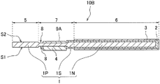
- a solid electrolytic capacitor according to this exemplary embodiment is similar to the solid electrolytic capacitor of the second exemplary embodiment except that capacitor elements 10 B each have second insulating layer 9 A disposed on a part of a second main surface of separation section 1 S of an anode body.
- FIG. 6A is a schematic cross-sectional view illustrating capacitor element 10 B according to the third exemplary embodiment. This configuration helps to more effectively prevent the occurrence of a short circuit between the capacitor elements.
- a solid electrolytic capacitor according to this exemplary embodiment is similar to the solid electrolytic capacitor of the second exemplary embodiment except that capacitor elements 10 C each have second insulating layer 9 B.
- Second insulating layer 9 B is disposed on second main surface S 2 of each anode body such that second insulating layer 9 B is put on a part of separation section 1 S and a part of anode section 1 P of the anode body, as well as a part of a cathode layer (solid electrolyte layer 2 and/or cathode lead-out layer 3 ) formed on second main surface S 2 of cathode formation section 1 N.
- FIG. 6B is a schematic cross-sectional view illustrating capacitor element 10 C according to the fourth exemplary embodiment. This configuration helps to more effectively prevent the occurrence of a short circuit between the capacitor elements and prevents degradation of the solid electrolyte layer.
- a solid electrolytic capacitor according to any of the exemplary embodiments is manufactured by a method including steps below: a first step of preparing a foil-shaped anode body that has a dielectric layer as well as a first main surface and a second main surface opposite to each other; a second step of forming a first insulating layer on each of the first and the second main surfaces at a position by which the anode body is separated into two regions; a third step of forming a solid electrolyte layer and a cathode lead-out layer on both the first and the second main surfaces of one of the regions; a fourth step of removing, after the third step, the first insulating layer from the second main surface to obtain a capacitor element; and a fifth step of stacking a plurality of the capacitor elements.
- An anode body containing metallic foil is made by a known method.
- the anode body is obtained, for example, by roughening a surface of a foil-shaped substrate that contains a valve metal.
- the roughening is satisfactory as long as irregularities are formed on the surface of the substrate and may be performed, for example, by subjecting the surface of the substrate to etching (e.g., electrolytic etching) or by depositing particles of the conductive material on the surface of the substrate by use of a gas phase method such as vapor deposition.
- a dielectric layer is formed on a surface of the anode body.
- the dielectric layer is formed by anodizing the surface of the anode body.
- the anodization can be performed by a known method, for example, an anodizing treatment.
- the anodizing treatment can be performed by, for example, immersing the anode body in an anodizing solution to impregnate the anode body with the anodizing solution and applying a voltage between the anode body as an anode and a cathode immersed in the anodizing solution.
- a process (a seventh step) for forming a recess on a separation section of the anode body may be performed before a second step described later.
- This process includes compressing, in a thickness direction of the anode body, a portion where the separation section is to be formed through press working or other processing so as to depress a first main surface and a second main surface of the anode body.
- the formed recess helps to prevent a solid electrolyte layer from crawling up in a third step.
- a first insulating layer is formed on each of the first and the second main surfaces at a position by which the obtained anode body is separated into two regions.
- the first insulating layer may be formed by applying a first liquid insulating material containing an insulating resin to a predetermined location or by sticking a first insulation tape substance containing an insulating resin onto the predetermined location.
- the first insulating layer should be formed from the first insulation tape substance. This makes formation of the first insulating layer easier and facilitates removal of the first insulating layer disposed on one of the main surfaces in a fourth step.
- the solid electrolyte layer containing the conductive polymer may be formed, for example, by a method of impregnating a material with a monomer or an oligomer and polymerizing the material chemically or electrolytically.
- a solid electrolyte layer may be formed by impregnating a material with a conductive polymer solution or dispersion liquid and drying the material.
- cathode lead-out layer made up of a carbon layer and a silver paste layer is formed.
- the cathode lead-out layer is not limited to this configuration and is satisfactory as long as the cathode lead-out layer has a function of current collection.
- the first insulating layer formed on the second main surface is removed.
- No particular limitation is placed on a method of removing the first insulating layer.
- a first insulating layer formed from the first insulation tape substance may be detached gradually from an end of the tape substance.
- a process may be performed to form a second insulating layer that is thinner than the first insulating layer on the second main surface at the position from which the first insulating layer has been removed.
- the second insulating layer may as well be formed by applying a second liquid insulating material to a predetermined location or by sticking a second insulation tape substance onto the predetermined location.
- a second insulating layer may be disposed on the second main surface instead of disposing the first insulating layer.
- the fourth and the sixth steps can be omitted.
- a preferable method should include forming a second insulating layer after processes of forming a first insulating layer on a second main surface, forming a cathode layer, and removing the first insulating layer.
- a plurality of capacitor elements that each include the first insulating layer and the second insulating layer formed on the anode body as described above are stacked so as to form a capacitor element group.
- the capacitor elements in the capacitor element group are stacked such that the first insulating layer of one of the mutually adjacent capacitor elements faces the second main surface (or the second insulating layer) of the other adjacent capacitor element.
- the second main surface of the other adjacent capacitor element has no first insulating layer because the first insulating layer formed on the second main surface is removed.
- the anode regions of the capacitor elements are swaged by a swaging component or welded together such that these regions are electrically connected to each other.
- an anode terminal and a cathode terminal are joined respectively to the anode region and the cathode region of any capacitor element of the capacitor element group.
- the capacitor element group is encapsulated in an exterior body so that a solid electrolytic capacitor is manufactured.
- a solid electrolytic capacitor according to the present disclosure allows the disposition of more capacitor elements in a limited space and offers high performance in preventing positional discrepancy and short circuits.
- the solid electrolytic capacitor can be used in various applications.
Landscapes
- Engineering & Computer Science (AREA)
- Power Engineering (AREA)
- Microelectronics & Electronic Packaging (AREA)
- Manufacturing & Machinery (AREA)
- Fixed Capacitors And Capacitor Manufacturing Machines (AREA)
- Electric Double-Layer Capacitors Or The Like (AREA)
Abstract
Description
Claims (6)
Priority Applications (1)
| Application Number | Priority Date | Filing Date | Title |
|---|---|---|---|
| US17/083,888 US11443903B2 (en) | 2015-10-28 | 2020-10-29 | Solid electrolytic capacitor having an insulating layer between exposed anode portions |
Applications Claiming Priority (3)
| Application Number | Priority Date | Filing Date | Title |
|---|---|---|---|
| JP2015-211890 | 2015-10-28 | ||
| JP2015211890 | 2015-10-28 | ||
| PCT/JP2016/004620 WO2017073032A1 (en) | 2015-10-28 | 2016-10-19 | Solid electrolytic capacitor and method for manufacturing solid electrolytic capacitor |
Related Parent Applications (1)
| Application Number | Title | Priority Date | Filing Date |
|---|---|---|---|
| PCT/JP2016/004620 Continuation WO2017073032A1 (en) | 2015-10-28 | 2016-10-19 | Solid electrolytic capacitor and method for manufacturing solid electrolytic capacitor |
Related Child Applications (1)
| Application Number | Title | Priority Date | Filing Date |
|---|---|---|---|
| US17/083,888 Continuation US11443903B2 (en) | 2015-10-28 | 2020-10-29 | Solid electrolytic capacitor having an insulating layer between exposed anode portions |
Publications (2)
| Publication Number | Publication Date |
|---|---|
| US20180233294A1 US20180233294A1 (en) | 2018-08-16 |
| US10861653B2 true US10861653B2 (en) | 2020-12-08 |
Family
ID=58631512
Family Applications (2)
| Application Number | Title | Priority Date | Filing Date |
|---|---|---|---|
| US15/945,789 Active 2037-01-25 US10861653B2 (en) | 2015-10-28 | 2018-04-05 | Solid electrolytic capacitor and method for manufacturing solid electrolytic capacitor with separation and insulation |
| US17/083,888 Active US11443903B2 (en) | 2015-10-28 | 2020-10-29 | Solid electrolytic capacitor having an insulating layer between exposed anode portions |
Family Applications After (1)
| Application Number | Title | Priority Date | Filing Date |
|---|---|---|---|
| US17/083,888 Active US11443903B2 (en) | 2015-10-28 | 2020-10-29 | Solid electrolytic capacitor having an insulating layer between exposed anode portions |
Country Status (4)
| Country | Link |
|---|---|
| US (2) | US10861653B2 (en) |
| JP (1) | JP6865352B2 (en) |
| CN (2) | CN112420395B (en) |
| WO (1) | WO2017073032A1 (en) |
Families Citing this family (7)
| Publication number | Priority date | Publication date | Assignee | Title |
|---|---|---|---|---|
| JP2019140255A (en) * | 2018-02-09 | 2019-08-22 | パナソニックIpマネジメント株式会社 | Electrolytic capacitor and manufacturing method thereof |
| JP7257636B2 (en) * | 2018-10-12 | 2023-04-14 | パナソニックIpマネジメント株式会社 | Solid electrolytic capacitor and manufacturing method thereof |
| CN116564711A (en) | 2019-01-24 | 2023-08-08 | 松下知识产权经营株式会社 | Solid electrolytic capacitor and manufacturing method thereof |
| JP7180561B2 (en) * | 2019-03-29 | 2022-11-30 | 株式会社村田製作所 | Capacitor arrays and composite electronic components |
| CN115280443B (en) * | 2020-03-25 | 2025-03-28 | 松下知识产权经营株式会社 | Electrolytic capacitors and capacitor components |
| JP7756312B2 (en) * | 2020-07-07 | 2025-10-20 | パナソニックIpマネジメント株式会社 | Solid electrolytic capacitor element, solid electrolytic capacitor and method for manufacturing the same |
| CN116888697A (en) | 2021-02-25 | 2023-10-13 | 松下知识产权经营株式会社 | Electrolytic capacitor and manufacturing method thereof |
Citations (16)
| Publication number | Priority date | Publication date | Assignee | Title |
|---|---|---|---|---|
| US6320742B1 (en) * | 1999-02-17 | 2001-11-20 | Matsushita Electric Industrial Co., Ltd. | Solid electrolytic capacitor, and method of manufacturing the same |
| US20040027789A1 (en) | 2002-06-07 | 2004-02-12 | Ayumi Kochi | Solid electrolytic capacitor |
| JP2004088073A (en) | 2002-06-07 | 2004-03-18 | Matsushita Electric Ind Co Ltd | Solid electrolytic capacitors |
| JP2006156681A (en) * | 2004-11-29 | 2006-06-15 | Tdk Corp | Solid electrolytic capacitor |
| US20070247781A1 (en) * | 2006-04-21 | 2007-10-25 | Sanyo Electric Co., Ltd. | Multi-layered solid electrolytic capacitor and method of manufacturing same |
| US7289314B2 (en) * | 2002-08-30 | 2007-10-30 | Showa Denko K.K. | Metal foil for capacitor, solid electrolytic capacitor using the foil and production methods of the foil and the capacitor |
| JP2008066430A (en) | 2006-09-06 | 2008-03-21 | Tdk Corp | Manufacturing method of solid electrolytic capacitor |
| JP2008262950A (en) * | 2007-04-10 | 2008-10-30 | Matsushita Electric Ind Co Ltd | Manufacturing method of solid electrolytic capacitor and manufacturing apparatus used therefor |
| US20090080144A1 (en) * | 2005-05-18 | 2009-03-26 | Sanyo Electric Co., Ltd. | Multi-layered solid electrolytic capacitor and method of manufacturing same |
| US20090135550A1 (en) * | 2007-11-26 | 2009-05-28 | Sanyo Electric Co., Ltd. | Solid electrolytic capacitor |
| JP2009129936A (en) | 2007-11-20 | 2009-06-11 | Nec Tokin Corp | Surface mounting thin-type capacitor and method of manufacturing the same |
| WO2009104377A1 (en) * | 2008-02-21 | 2009-08-27 | 三洋電機株式会社 | Solid electrolytic capacitor and method for manufacturing the same |
| JP2009194263A (en) | 2008-02-18 | 2009-08-27 | Sanyo Electric Co Ltd | Manufacturing method of solid electrolytic capacitor |
| JP2010177467A (en) * | 2009-01-29 | 2010-08-12 | Sanyo Electric Co Ltd | Solid-state electrolytic capacitor element |
| JP2011249632A (en) * | 2010-05-28 | 2011-12-08 | Nichicon Corp | Substrate for solid electrolytic capacitor and method for manufacturing the same, single plate solid electrolytic capacitor element and method for manufacturing the same, and multilayer solid electrolytic capacitor and method for manufacturing the same |
| US20130010404A1 (en) * | 2011-07-07 | 2013-01-10 | Apaq Technology Co., Ltd. | Capacitance unit and stacked solid electrolytic capacitor |
Family Cites Families (7)
| Publication number | Priority date | Publication date | Assignee | Title |
|---|---|---|---|---|
| JP4547835B2 (en) * | 2001-06-21 | 2010-09-22 | パナソニック株式会社 | Solid electrolytic capacitor and manufacturing method thereof |
| TWI283879B (en) * | 2005-02-17 | 2007-07-11 | Sanyo Electric Co | Solid electrolytic capacitor and manufacturing method thereof |
| JP5274340B2 (en) * | 2009-03-31 | 2013-08-28 | 三洋電機株式会社 | Solid electrolytic capacitor |
| CN103003901B (en) * | 2010-08-02 | 2016-03-09 | 松下知识产权经营株式会社 | Solid electrolytic capacitor |
| CN103959413B (en) * | 2011-12-14 | 2017-11-24 | 株式会社村田制作所 | Solid electrolytic capacitor And Manufacturing approach |
| JP5585618B2 (en) * | 2012-07-03 | 2014-09-10 | 株式会社村田製作所 | Solid electrolytic capacitor and manufacturing method thereof |
| WO2015040883A1 (en) * | 2013-09-20 | 2015-03-26 | 株式会社村田製作所 | Method for manufacturing solid electrolytic capacitor |
-
2016
- 2016-10-19 CN CN202011175946.3A patent/CN112420395B/en active Active
- 2016-10-19 JP JP2017547607A patent/JP6865352B2/en active Active
- 2016-10-19 WO PCT/JP2016/004620 patent/WO2017073032A1/en not_active Ceased
- 2016-10-19 CN CN201680061543.1A patent/CN108140493B/en active Active
-
2018
- 2018-04-05 US US15/945,789 patent/US10861653B2/en active Active
-
2020
- 2020-10-29 US US17/083,888 patent/US11443903B2/en active Active
Patent Citations (16)
| Publication number | Priority date | Publication date | Assignee | Title |
|---|---|---|---|---|
| US6320742B1 (en) * | 1999-02-17 | 2001-11-20 | Matsushita Electric Industrial Co., Ltd. | Solid electrolytic capacitor, and method of manufacturing the same |
| US20040027789A1 (en) | 2002-06-07 | 2004-02-12 | Ayumi Kochi | Solid electrolytic capacitor |
| JP2004088073A (en) | 2002-06-07 | 2004-03-18 | Matsushita Electric Ind Co Ltd | Solid electrolytic capacitors |
| US7289314B2 (en) * | 2002-08-30 | 2007-10-30 | Showa Denko K.K. | Metal foil for capacitor, solid electrolytic capacitor using the foil and production methods of the foil and the capacitor |
| JP2006156681A (en) * | 2004-11-29 | 2006-06-15 | Tdk Corp | Solid electrolytic capacitor |
| US20090080144A1 (en) * | 2005-05-18 | 2009-03-26 | Sanyo Electric Co., Ltd. | Multi-layered solid electrolytic capacitor and method of manufacturing same |
| US20070247781A1 (en) * | 2006-04-21 | 2007-10-25 | Sanyo Electric Co., Ltd. | Multi-layered solid electrolytic capacitor and method of manufacturing same |
| JP2008066430A (en) | 2006-09-06 | 2008-03-21 | Tdk Corp | Manufacturing method of solid electrolytic capacitor |
| JP2008262950A (en) * | 2007-04-10 | 2008-10-30 | Matsushita Electric Ind Co Ltd | Manufacturing method of solid electrolytic capacitor and manufacturing apparatus used therefor |
| JP2009129936A (en) | 2007-11-20 | 2009-06-11 | Nec Tokin Corp | Surface mounting thin-type capacitor and method of manufacturing the same |
| US20090135550A1 (en) * | 2007-11-26 | 2009-05-28 | Sanyo Electric Co., Ltd. | Solid electrolytic capacitor |
| JP2009194263A (en) | 2008-02-18 | 2009-08-27 | Sanyo Electric Co Ltd | Manufacturing method of solid electrolytic capacitor |
| WO2009104377A1 (en) * | 2008-02-21 | 2009-08-27 | 三洋電機株式会社 | Solid electrolytic capacitor and method for manufacturing the same |
| JP2010177467A (en) * | 2009-01-29 | 2010-08-12 | Sanyo Electric Co Ltd | Solid-state electrolytic capacitor element |
| JP2011249632A (en) * | 2010-05-28 | 2011-12-08 | Nichicon Corp | Substrate for solid electrolytic capacitor and method for manufacturing the same, single plate solid electrolytic capacitor element and method for manufacturing the same, and multilayer solid electrolytic capacitor and method for manufacturing the same |
| US20130010404A1 (en) * | 2011-07-07 | 2013-01-10 | Apaq Technology Co., Ltd. | Capacitance unit and stacked solid electrolytic capacitor |
Non-Patent Citations (1)
| Title |
|---|
| International Search Report of PCT application No. PCT/JP2016/004620 dated Jan. 10, 2017. |
Also Published As
| Publication number | Publication date |
|---|---|
| US11443903B2 (en) | 2022-09-13 |
| CN112420395B (en) | 2022-10-04 |
| US20180233294A1 (en) | 2018-08-16 |
| CN112420395A (en) | 2021-02-26 |
| CN108140493B (en) | 2020-11-17 |
| WO2017073032A1 (en) | 2017-05-04 |
| US20210043393A1 (en) | 2021-02-11 |
| CN108140493A (en) | 2018-06-08 |
| JP6865352B2 (en) | 2021-04-28 |
| JPWO2017073032A1 (en) | 2018-08-23 |
Similar Documents
| Publication | Publication Date | Title |
|---|---|---|
| US11443903B2 (en) | Solid electrolytic capacitor having an insulating layer between exposed anode portions | |
| JP7706069B2 (en) | Electrolytic capacitor and its manufacturing method | |
| US6215651B1 (en) | Solid electrolyte capacitor using conductive polymer | |
| US11127533B2 (en) | Solid electrolytic capacitor and method for manufacturing same | |
| JP2023053310A (en) | Electrolytic capacitor and manufacturing method thereof | |
| JP4478695B2 (en) | Solid electrolytic capacitor element and solid electrolytic capacitor including the same | |
| JP6747512B2 (en) | Solid electrolytic capacitor | |
| WO2018066254A1 (en) | Solid electrolytic capacitor | |
| CN110168687B (en) | Solid electrolytic capacitor | |
| JP2024097092A (en) | Electrolytic capacitor | |
| JP4867667B2 (en) | Solid electrolytic capacitor | |
| US10655241B2 (en) | Electrode foil production method and capacitor production method | |
| US8882857B2 (en) | Solid electrolytic capacitor and method for manufacturing the same | |
| US12154728B2 (en) | Capacitor element, electrolytic capacitor, and methods for manufacturing same | |
| WO2019058535A1 (en) | Solid electrolytic capacitor and method for manufacturing same | |
| JP4671339B2 (en) | Multilayer solid electrolytic capacitor | |
| CN114981905A (en) | Electrolytic capacitor | |
| JP2005079520A (en) | Coin-shaped solid electrolytic capacitor | |
| JP2002050542A (en) | Chip type multilayer capacitor |
Legal Events
| Date | Code | Title | Description |
|---|---|---|---|
| FEPP | Fee payment procedure |
Free format text: ENTITY STATUS SET TO UNDISCOUNTED (ORIGINAL EVENT CODE: BIG.); ENTITY STATUS OF PATENT OWNER: LARGE ENTITY |
|
| AS | Assignment |
Owner name: PANASONIC INTELLECTUAL PROPERTY MANAGEMENT CO., LTD., JAPAN Free format text: ASSIGNMENT OF ASSIGNORS INTEREST;ASSIGNORS:ISHIZAKI, KATSUHISA;AMIUCHI, YUTA;YAMAMURA, YOSHIO;SIGNING DATES FROM 20180319 TO 20180322;REEL/FRAME:046152/0161 Owner name: PANASONIC INTELLECTUAL PROPERTY MANAGEMENT CO., LT Free format text: ASSIGNMENT OF ASSIGNORS INTEREST;ASSIGNORS:ISHIZAKI, KATSUHISA;AMIUCHI, YUTA;YAMAMURA, YOSHIO;SIGNING DATES FROM 20180319 TO 20180322;REEL/FRAME:046152/0161 |
|
| STPP | Information on status: patent application and granting procedure in general |
Free format text: DOCKETED NEW CASE - READY FOR EXAMINATION |
|
| STPP | Information on status: patent application and granting procedure in general |
Free format text: NON FINAL ACTION MAILED |
|
| STPP | Information on status: patent application and granting procedure in general |
Free format text: RESPONSE TO NON-FINAL OFFICE ACTION ENTERED AND FORWARDED TO EXAMINER |
|
| STPP | Information on status: patent application and granting procedure in general |
Free format text: FINAL REJECTION MAILED |
|
| STPP | Information on status: patent application and granting procedure in general |
Free format text: DOCKETED NEW CASE - READY FOR EXAMINATION |
|
| STPP | Information on status: patent application and granting procedure in general |
Free format text: NOTICE OF ALLOWANCE MAILED -- APPLICATION RECEIVED IN OFFICE OF PUBLICATIONS |
|
| STCF | Information on status: patent grant |
Free format text: PATENTED CASE |
|
| MAFP | Maintenance fee payment |
Free format text: PAYMENT OF MAINTENANCE FEE, 4TH YEAR, LARGE ENTITY (ORIGINAL EVENT CODE: M1551); ENTITY STATUS OF PATENT OWNER: LARGE ENTITY Year of fee payment: 4 |