US10858246B2 - Semiconductor device, microphone and methods for forming a semiconductor device - Google Patents
Semiconductor device, microphone and methods for forming a semiconductor device Download PDFInfo
- Publication number
- US10858246B2 US10858246B2 US15/901,196 US201815901196A US10858246B2 US 10858246 B2 US10858246 B2 US 10858246B2 US 201815901196 A US201815901196 A US 201815901196A US 10858246 B2 US10858246 B2 US 10858246B2
- Authority
- US
- United States
- Prior art keywords
- metal layer
- structured metal
- layer
- semiconductor device
- covering layer
- Prior art date
- Legal status (The legal status is an assumption and is not a legal conclusion. Google has not performed a legal analysis and makes no representation as to the accuracy of the status listed.)
- Active, expires
Links
Images


Classifications
-
- B—PERFORMING OPERATIONS; TRANSPORTING
- B81—MICROSTRUCTURAL TECHNOLOGY
- B81C—PROCESSES OR APPARATUS SPECIALLY ADAPTED FOR THE MANUFACTURE OR TREATMENT OF MICROSTRUCTURAL DEVICES OR SYSTEMS
- B81C1/00—Manufacture or treatment of devices or systems in or on a substrate
- B81C1/00777—Preserve existing structures from alteration, e.g. temporary protection during manufacturing
- B81C1/00785—Avoid chemical alteration, e.g. contamination, oxidation or unwanted etching
- B81C1/00801—Avoid alteration of functional structures by etching, e.g. using a passivation layer or an etch stop layer
-
- H—ELECTRICITY
- H04—ELECTRIC COMMUNICATION TECHNIQUE
- H04R—LOUDSPEAKERS, MICROPHONES, GRAMOPHONE PICK-UPS OR LIKE ACOUSTIC ELECTROMECHANICAL TRANSDUCERS; ELECTRIC HEARING AIDS; PUBLIC ADDRESS SYSTEMS
- H04R19/00—Electrostatic transducers
- H04R19/005—Electrostatic transducers using semiconductor materials
-
- H—ELECTRICITY
- H04—ELECTRIC COMMUNICATION TECHNIQUE
- H04R—LOUDSPEAKERS, MICROPHONES, GRAMOPHONE PICK-UPS OR LIKE ACOUSTIC ELECTROMECHANICAL TRANSDUCERS; ELECTRIC HEARING AIDS; PUBLIC ADDRESS SYSTEMS
- H04R19/00—Electrostatic transducers
- H04R19/04—Microphones
-
- H—ELECTRICITY
- H04—ELECTRIC COMMUNICATION TECHNIQUE
- H04R—LOUDSPEAKERS, MICROPHONES, GRAMOPHONE PICK-UPS OR LIKE ACOUSTIC ELECTROMECHANICAL TRANSDUCERS; ELECTRIC HEARING AIDS; PUBLIC ADDRESS SYSTEMS
- H04R31/00—Apparatus or processes specially adapted for the manufacture of transducers or diaphragms therefor
-
- B—PERFORMING OPERATIONS; TRANSPORTING
- B81—MICROSTRUCTURAL TECHNOLOGY
- B81C—PROCESSES OR APPARATUS SPECIALLY ADAPTED FOR THE MANUFACTURE OR TREATMENT OF MICROSTRUCTURAL DEVICES OR SYSTEMS
- B81C2201/00—Manufacture or treatment of microstructural devices or systems
- B81C2201/01—Manufacture or treatment of microstructural devices or systems in or on a substrate
- B81C2201/0101—Shaping material; Structuring the bulk substrate or layers on the substrate; Film patterning
- B81C2201/0128—Processes for removing material
- B81C2201/013—Etching
- B81C2201/0133—Wet etching
-
- B—PERFORMING OPERATIONS; TRANSPORTING
- B81—MICROSTRUCTURAL TECHNOLOGY
- B81C—PROCESSES OR APPARATUS SPECIALLY ADAPTED FOR THE MANUFACTURE OR TREATMENT OF MICROSTRUCTURAL DEVICES OR SYSTEMS
- B81C2201/00—Manufacture or treatment of microstructural devices or systems
- B81C2201/01—Manufacture or treatment of microstructural devices or systems in or on a substrate
- B81C2201/0174—Manufacture or treatment of microstructural devices or systems in or on a substrate for making multi-layered devices, film deposition or growing
- B81C2201/0176—Chemical vapour Deposition
-
- B—PERFORMING OPERATIONS; TRANSPORTING
- B81—MICROSTRUCTURAL TECHNOLOGY
- B81C—PROCESSES OR APPARATUS SPECIALLY ADAPTED FOR THE MANUFACTURE OR TREATMENT OF MICROSTRUCTURAL DEVICES OR SYSTEMS
- B81C2201/00—Manufacture or treatment of microstructural devices or systems
- B81C2201/05—Temporary protection of devices or parts of the devices during manufacturing
- B81C2201/053—Depositing a protective layers
-
- B—PERFORMING OPERATIONS; TRANSPORTING
- B81—MICROSTRUCTURAL TECHNOLOGY
- B81C—PROCESSES OR APPARATUS SPECIALLY ADAPTED FOR THE MANUFACTURE OR TREATMENT OF MICROSTRUCTURAL DEVICES OR SYSTEMS
- B81C2201/00—Manufacture or treatment of microstructural devices or systems
- B81C2201/05—Temporary protection of devices or parts of the devices during manufacturing
- B81C2201/056—Releasing structures at the end of the manufacturing process
-
- H—ELECTRICITY
- H04—ELECTRIC COMMUNICATION TECHNIQUE
- H04R—LOUDSPEAKERS, MICROPHONES, GRAMOPHONE PICK-UPS OR LIKE ACOUSTIC ELECTROMECHANICAL TRANSDUCERS; ELECTRIC HEARING AIDS; PUBLIC ADDRESS SYSTEMS
- H04R2201/00—Details of transducers, loudspeakers or microphones covered by H04R1/00 but not provided for in any of its subgroups
- H04R2201/003—Mems transducers or their use
Definitions
- a semiconductor device often comprises a structured metal layer. It may be desirable to passivate at least parts of the structured metal layer in order to increase a lifetime of the structured metal layer and thus of the semiconductor device.
- the semiconductor device comprises a structured metal layer.
- the structured metal layer lies above a semiconductor substrate.
- a thickness of the structured metal layer is more than 100 nm.
- the semiconductor device comprises a covering layer.
- the covering layer lies adjacent to at least one part of a front side of the structured metal layer and adjacent to a side wall of the structured metal layer.
- the covering layer comprises amorphous silicon carbide.
- Some examples relate to a microphone comprising a semiconductor device.
- Some examples relate to a method for forming a semiconductor device.
- the method comprises forming a structured metal layer above a semiconductor substrate.
- a thickness of the structured metal layer is more than 100 nm.
- the method comprises forming a covering layer after forming the structured metal layer, such that the covering layer lies adjacent to a front side of the structured metal layer and adjacent to a side wall of the structured metal layer.
- the covering layer comprises amorphous silicon carbide.
- Some examples relate to a method for forming a semiconductor device.
- the method comprises forming a structured metal layer above a semiconductor substrate.
- a thickness of the structured metal layer is more than 100 nm.
- the method comprises forming a covering layer by means of plasma deposition after forming the structured metal layer, such that the covering layer lies adjacent to a front side of the structured metal layer and adjacent to a side wall of the structured metal layer.
- Helium is used as dilution gas during the plasma deposition.
- FIG. 1 shows a schematic cross section of part of a semiconductor device
- FIG. 2 shows a schematic cross section of part of a further semiconductor device
- FIG. 3 shows a schematic cross section of part of a microphone
- FIG. 4 shows a schematic plan view of part of a further microphone
- FIG. 5 shows a flow diagram of a method for forming a semiconductor device
- FIG. 6 shows a flow diagram of a further method for forming a semiconductor device.
- identical reference signs may designate identical or comparable components.
- collective reference signs may be used for components and objects which occur multiply in an exemplary embodiment or in a drawing but are described jointly with regard to one or more features.
- Components or objects described with identical or collective reference signs, with regard to individual, a plurality or all of the features, for example their dimensionings, may be embodied identically, but possibly also differently, unless the description explicitly or implicitly reveals something else.
- one element referred to as being “connected” or “coupled” to another element may be directly connected or coupled to the other element or intervening elements may be present. If two elements A and B are combined by an “or”, then this should be understood to include all possible combinations, for example “only A”, “only B” and “A and B”. An alternative formulation for the same combination is “at least one of A and B”. The same applies to combinations of more than two elements.
- FIG. 1 shows a schematic cross section of part of a semiconductor device 100 .
- the semiconductor device 100 comprises a structured metal layer 110 .
- the structured metal layer 110 lies above a semiconductor substrate 120 .
- a thickness of the structured metal layer 110 is more than 100 nm (or more than 500 nm or more than 1 m).
- the semiconductor device 100 comprises a covering layer 130 .
- the covering layer 130 lies adjacent to at least one part of a front side 111 of the structured metal layer 110 and adjacent to a side wall 112 of the structured metal layer 110 .
- the covering layer 130 comprises amorphous silicon carbide.
- a covering layer comprising amorphous silicon carbide can be produced particularly tightly and/or reliably in comparison with a covering layer composed of a different material.
- the use of amorphous silicon carbide as material for the covering layer 130 makes it possible to prevent a seam line from arising in the covering layer 130 at a transition between the front side 111 and the side wall 112 of the structured metal layer 110 or at a steep topography step of the covering layer 130 .
- a passivation of the structured metal layer 110 can be improved as a result. This makes it possible to reduce corrosion of the structured metal layer 110 as a result of subsequent production process steps or during operation. A lifetime of the semiconductor device can be increased as a result.
- the structured metal layer 110 can be formed from a cost-effective base metal. A more cost-effective semiconductor device can be provided as a result.
- the covering layer 130 can be an amorphous silicon carbide layer.
- the amorphous silicon carbide layer can contain for example at least 50% (or at least 60%, at least 70%, at least 80%, at least 90% or at least 95%) amorphous silicon carbide (a-SiC).
- a-SiC amorphous silicon carbide
- the amorphous silicon carbide layer can have a 1:1 ratio of carbon (C) to silicon (Si).
- the amorphous silicon carbide layer can also have other ratios of the elements carbon to silicon, for example 0.8:1.2 or 0.7:1.3).
- the amorphous silicon carbide layer can contain atomic hydrogen (H).
- the amorphous silicon carbide layer can contain nitrogen (N), for example.
- the amorphous silicon carbide layer can be an amorphous SiC:N layer.
- the covering layer 130 can be constructed as a multilayer (for example having 1-10000 plies). At least some of the plies of the multilayer can be amorphous silicon carbide plies.
- plies of the multilayer (for example the amorphous silicon carbide plies) can be arranged with many changes of stoichiometry etc., in alternation.
- the multilayer can comprise for example a combination of amorphous silicon carbide plies or amorphous silicon carbide layers with other plies (for example nitride plies or oxide plies) or layers (for example nitride layers or oxide layers).
- the covering layer 130 can be an amorphous silicon carbide-like layer which was formed at low temperatures (owing to metallization that is present) and has an excellent edge coverage (for example at a transition between the front side 111 and the side wall 112 ) without seam lines.
- Traditional plasma nitrides of silicon can fail here at the edges (for example at a transition between the front side 111 and the side wall 112 ).
- the covering layer 130 and/or the amorphous silicon carbide layer can be part of a layer composite.
- the covering layer 130 can have a thickness of more than 10 nm (or more than 100 nm, more than 1 ⁇ m, or more than 10 ⁇ m) and/or of less than 200 ⁇ m (or less than 100 ⁇ m or less than 50 ⁇ m).
- an (electrical) resistivity of the covering layer 130 can be more than 1*10 10 ⁇ cm (or more than 5*10 10 ⁇ cm) and less than 1*10 12 ⁇ cm (or less than 5*10 11 ⁇ cm).
- the front side 111 of the structured metal layer 110 can be a side of the structured metal layer 110 facing away from the semiconductor substrate 120 .
- a rear side of the structured metal layer 110 can be for example a side of the structured metal layer 110 facing the semiconductor substrate 120 .
- the side wall 112 of the structured metal layer 110 can extend from the front side 111 of the structured metal layer 110 as far as the rear side of the structured metal layer 110 or as far as an insulation layer on which the structured metal layer 110 is arranged.
- the side wall 112 of the structured metal layer 110 can have for example an average gradient angle of more than 200 (or more than 30°, more than 45°, more than 60°, more than 70°, more than 80° or more than 85°).
- the average gradient angle of the side wall 112 can be an angle of the side wall 112 at half the thickness of the structured metal layer 110 .
- the side wall 112 of the structured metal layer 110 can for example be steep or extend almost perpendicularly to the front side 111 of the structured metal layer 110 or a front side of the semiconductor substrate 120 .
- the front side 111 of the structured metal layer 110 can extend parallel to the front side of the semiconductor substrate 120 .
- the structured metal layer 110 can form for example a step above the semiconductor substrate 120 .
- an insulation layer can lie below the structured metal layer 110 and above the semiconductor substrate 120 and thus between the structured metal layer 110 and the semiconductor substrate 120 .
- the structured metal layer 110 can be electrically insulated from the semiconductor substrate 120 in an efficient manner.
- a thickness of the insulation layer can be more than 1 ⁇ m (or more than 10 ⁇ m or more than 100 m).
- the insulation layer can be for example an oxide layer (for example a silicon oxide (SiO 2 ) layer) or a nitride layer (for example a silicon nitride (Si 3 N 4 ) layer).
- the structured metal layer 110 can be arranged on the oxide layer or the nitride layer.
- the structured metal layer 110 can be at least one from an aluminum layer, an aluminum alloy layer, a copper layer and a copper alloy layer.
- a cost-effective material for the structured metal layer 110 it is possible for the semiconductor device 100 to be provided cost-effectively.
- the aluminum layer, the aluminum alloy layer, the copper layer or the copper alloy layer can replace a gold (Au) layer.
- the aluminum layer can contain at least 80% (or at least 90% or at least 95%) aluminum (Al).
- the copper layer can contain for example at least 80% (or at least 90% or at least 95%) copper (Cu).
- the aluminum alloy layer can be an aluminum-copper (AlCu) layer.
- the semiconductor device 100 can furthermore comprise a microelectromechanical element.
- the structured metal layer 110 can form a connection pad (for example a bond pad) for the electrical contacting of the microelectromechanical element.
- the semiconductor device 100 can form a Micro-Electro-Mechanical System (MEMS) device or be an element of a MEMS device (for example of a microphone or of a pressure sensor).
- MEMS Micro-Electro-Mechanical System
- part of the semiconductor device 100 can be put at a specific potential (for example at a ground potential) via the structured metal pad 110 .
- the structured metal pad 110 can be electrically conductively connected to a control circuit and the part of the semiconductor device 100 .
- the microelectromechanical element can comprise a membrane structure.
- the membrane structure can be arranged above a cutout formed in or on the semiconductor substrate 120 .
- the covering layer 130 can be used as a protective layer for the structured metal layer 110 during a process of forming the cutout in the semiconductor substrate 120 (for example by means of an etching process) or removing a sacrificial layer below the membrane in order to free the membrane. It is thereby possible to increase a yield when forming a semiconductor device 100 . As a result, the semiconductor device 100 can be provided cost-effectively.
- the membrane structure can be a silicon membrane.
- the microelectromechanical element can comprise a MEMS oscillator and/or a MEMS gyroscope.
- the semiconductor device 100 can furthermore comprise a bond structure in contact with the structured metal layer 110 .
- the bond structure can comprise a bond wire or a solder ball.
- Part of the front side 111 of the structured metal layer 110 can be free of the covering layer 130 , for example, in order to be able to bring the bond structure into contact with the structured metal layer 110 .
- the semiconductor substrate 120 can be a silicon (Si)-based semiconductor substrate.
- the semiconductor substrate 120 can be a silicon carbide (SiC)-based semiconductor substrate, a gallium arsenide (GaAs)-based semiconductor substrate or a gallium nitride (GaN)-based semiconductor substrate.
- the semiconductor substrate 120 can be for example a semiconductor wafer or a semiconductor slice.
- a vertical direction, a vertical dimension or a thickness can be measured perpendicularly to the front side of the structured metal layer 110 or perpendicularly to a surface of the semiconductor substrate 120 and a lateral direction or a lateral dimension can be measured parallel to the front side of the structured metal layer 110 or to the surface of the semiconductor substrate 120 .
- a front side of the semiconductor substrate 120 can be for example a surface of the semiconductor substrate 120 on which structures that are intended to be produced are more complex than those on a rear side of the semiconductor substrate 120 since process parameters (for example a temperature) and a treatment of the rear side may be restricted if structures have already been formed on the front side.
- the semiconductor device 100 can be a microphone, a sensor component (for example a pressure sensor or an acceleration sensor), a MEMS component, a processor or a memory component.
- FIG. 2 shows a schematic cross section of part of a further semiconductor device 200 .
- the semiconductor device 200 can be embodied similarly to the semiconductor device 100 described in association with FIG. 1 .
- the semiconductor device 200 comprises a semiconductor substrate 120 .
- the semiconductor substrate 120 can be a silicon substrate.
- An oxide layer 210 lies adjacent to a front side 121 of the semiconductor substrate 120 .
- the oxide layer 210 can be a silicon oxide layer.
- a structured metal layer 110 lies adjacent to a surface 211 of the oxide layer 210 .
- the structured metal layer 110 can be an aluminum layer.
- the structured metal layer 110 can form a step, for example.
- a covering layer 130 lies adjacent to a front side 111 of the structured metal layer 110 , adjacent to a side wall 112 of the structured metal layer 110 and adjacent to the surface 211 of the oxide layer 210 .
- the covering layer 130 can comprise amorphous silicon carbide for example.
- FIG. 2 shows an example of a step covering of amorphous silicon carbide (SiC) on aluminum (Al).
- the semiconductor device 200 for example for a MEMS product such as a silicon (Si) microphone having aluminum (Al) metallization
- production of seam lines at topography steps can be avoided or at least reduced.
- Such seam lines are often not tight, for which reason the structured metal layer 110 (for example an aluminum (Al) step), during the release etching (for example by means of a buffered oxide etch), with seam lines possibly present, can be attacked by the etchant used (for example FAEL).
- the etchant used for example FAEL
- the covering layer 130 can comprise plasma-deposited amorphous silicon carbide (SiC).
- SiC plasma-deposited amorphous silicon carbide
- the covering layer 130 can also be used as passivation (for example of the structured metal layer 110 ).
- FIG. 2 can comprise one or more optional additional features corresponding to one or more aspects mentioned in connection with the proposed concept or one or more of the embodiments described above (for example FIG. 1 ) or below (for example FIGS. 3-6 ).
- FIG. 3 shows a schematic cross section of part of a microphone 300 .
- the microphone 300 comprises a semiconductor device.
- the semiconductor device can be embodied similarly to the semiconductor device 100 described in association with FIG. 1 or the semiconductor device 200 described in association with FIG. 2 .
- the microphone 300 comprises a semiconductor substrate 120 .
- the semiconductor substrate 120 can be a silicon substrate.
- An oxide layer 210 lies adjacent to the semiconductor substrate 120 .
- the oxide layer 210 can be a silicon oxide layer.
- a structured metal layer 110 lies adjacent to the oxide layer 210 .
- the structured metal layer 110 can be an aluminum layer.
- a covering layer 130 lies adjacent to the structured metal layer 110 and adjacent to the oxide layer 210 .
- the electrical connection structure 310 can comprise an electrically conductive material (for example aluminum, copper or polysilicon). As a result, the electrical connection structure 310 can electrically conductively connect the structured metal layer 110 to the membrane structure 320 .
- the structured metal layer 110 can thereby form a connection pad or a terminal pad for the membrane structure 320 .
- the membrane structure 320 is arranged above a cutout 330 formed in the semiconductor substrate 120 and the oxide layer 210 .
- the cutout 220 can form a cavity below the membrane structure 320 .
- the semiconductor substrate 120 additionally forms a base of the cutout 330 o .
- the cutout 330 can penetrate completely through the semiconductor substrate 120 .
- the microphone 300 comprises a counterelectrode 340 situated at the base of the cutout 330 .
- the microphone 300 can be a capacitor microphone.
- the membrane structure 320 and the counterelectrode 340 can form a capacitor. In the event of sound waves impinging on the membrane structure 320 , the latter can be caused to oscillate. A capacitance of the capacitor can change as a result of the oscillation of the membrane structure 320 .
- the microphone 300 can additionally comprise an evaluation circuit for detecting the change in the capacitance of the capacitor and for generating an analog or digital electrical signal representing the detected change in the capacitance and thus the impinging sound waves.
- the evaluation circuit can be implemented on the semiconductor substrate 120 or be an external circuit.
- FIG. 3 can comprise one or more optional additional features corresponding to one or more aspects mentioned in connection with the proposed concept or one or more of the embodiments described above (for example FIGS. 1-2 ) or below (for example FIGS. 4-6 ).
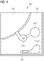
- FIG. 4 shows a schematic plan view of part of a further microphone 400 .
- the microphone can be embodied similarly to the microphone 300 described in association with FIG. 3 .
- the microphone 400 comprises a semiconductor substrate 120 .
- Two structured metal layers 110 are arranged above the semiconductor substrate 120 .
- the structured metal layer 110 - 1 is connected to a membrane structure 320 of the microphone 400 via an electrical connection structure 310 .
- the structured metal layer 110 - 2 is connected to a counterelectrode 340 (not depicted) of the microphone 400 .
- the structured metal layers 110 can form connection pads or terminal pads for the membrane structure 320 and the counterelectrode 340 .
- a covering layer 130 lies adjacent to the front sides 111 of the structured metal layers 110 and adjacent to the side walls 112 of the structured metal layers 110 .
- an oxide layer 210 (not depicted) can lie between the structured metal layers 110 and the semiconductor substrate.
- FIG. 4 shows an example of preventing an FAEL attack on an aluminum (Al) metallization by means of tight amorphous silicon carbide (SiC).
- FIG. 4 can comprise one or more optional additional features corresponding to one or more aspects mentioned in connection with the proposed concept or one or more of the embodiments described above (for example FIGS. 1-3 ) or below (for example FIGS. 5-6 ).
- FIG. 5 shows a flow diagram of a method 500 , for forming a semiconductor device.
- the method 500 comprises forming 510 a structured metal layer 110 above a semiconductor substrate 120 .
- a thickness of the structured metal layer 110 is more than 100 nm (or more than 500 nm or more than 1 ⁇ m).
- the method 500 comprises forming 520 a covering layer 130 after forming 510 the structured metal layer 110 , such that the covering layer 130 lies adjacent to a front side 111 of the structured metal layer 110 and adjacent to a side wall 112 of the structured metal layer 110 .
- the covering layer 130 comprises amorphous silicon carbide.
- a covering layer comprising amorphous silicon carbide can be produced particularly tightly and/or reliably in comparison with a covering layer composed of a different material.
- the use of amorphous silicon carbide as material for the covering layer 130 makes it possible to prevent a seam line from arising in the covering layer 130 at a transition between the front side 111 and the side wall 112 of the structured metal layer 110 or at a steep topography step of the covering layer 130 during the process of forming 520 .
- improved protection of the structured metal layer 110 during a subsequent etching process can be brought about by means of the covering layer 130 . It is thereby possible to avoid damage to the structured metal layer 110 during the etching process. As a result, a lifetime of the semiconductor device can be increased.
- the semiconductor device can be formed with a higher yield.
- the structured metal layer 110 can be formed from a cost-effective base metal.
- the semiconductor device can be formed cost-effectively.
- the covering layer 130 can be used as a passivation layer for the structured metal layer 110 . Formation of an additional passivation layer can thereby be obviated. As a result, the semiconductor device can be formed cost-effectively.
- the semiconductor device 100 described in association with FIG. 1 and/or the semiconductor device 200 described in association with FIG. 2 can be formed by means of the method 500 .
- forming 510 the structured metal layer 110 above the semiconductor substrate 120 can comprise depositing a metal layer on an insulation layer (for example an oxide layer 210 or a nitride layer) situated at the semiconductor substrate 120 , and structuring the deposited metal layer.
- Structuring the deposited metal layer can comprise for example applying a mask on the deposited metal layer and etching the masked metal layer.
- forming 520 the covering layer 130 can be carried out at a temperature of less than 450° C. (or less than 400° C. or less than 350° C.).
- the structured metal layer 110 can be formed from a metal having a low melting point (for example from aluminum). The semiconductor device can thereby be formed cost-effectively.
- the covering layer 130 can be formed by means of plasma deposition.
- the plasma deposition can be carried out at a pressure of less than 70 kPa (or less than 500 kPa, less than 25 kPa, less than 10 kPa or less than 1 kPa) or of less than 500 torr (or less than 250 torr, less than 100 torr, less than 50 torr, less than 25 torr or less than 8 torr).
- the oxide layer 210 can be an oxide layer formed by means of a tetraethyl orthosilicate (TEOS) method.
- the plasma deposition can be for example a plasma-enhanced chemical vapor deposition (PECVD).
- PECVD plasma-enhanced chemical vapor deposition
- the covering layer 130 at a deposition temperature of less than or equal to 400° C. can form a tight film (for example on the structured metal layer 110 ) and serve as passivation and step protection.
- the plasma deposition can comprise a capacitive plasma coupling into a parallel-plate capacitor of a plasma reactor.
- methane can be used as a carbon source during the plasma deposition.
- monosilane can be used as a silicon source during the plasma deposition.
- helium can be used as a dilution gas during the plasma deposition.
- a helium concentration during the plasma deposition can be more than 20% (or more than 30% or more than 50%).
- carbon atoms and silicon atoms can be present in the same concentration in the plasma reactor.
- amorphous silicon carbide can be deposited in a plasma reactor which can also be used for a silicon nitride (Si 3 N 4 ) deposition, for example. If the chemical composition is set in such a way that amorphous SiC is deposited, a film without seam lines can grow on steps with a steep side wall (for example on the structured metal layer 110 ). On account of the low deposition temperature during the SiC deposition, the process can be carried out after forming 510 the structured metal layer 110 (for example an aluminum (Al) metallization). In addition, in this process it is possible to achieve an excellent adhesion (for example of the covering layer 130 ) to the structured metal layer 110 (for example to aluminum) and to the oxide layer 210 (for example to a TEOS oxide).
- SiC silicon carbide
- Si 3 N 4 silicon nitride
- the covering layer 130 formed in the method step 520 can be a plasma-deposited, amorphous silicon carbide (SiC) film having excellent step coverage of 100% and the absence of seam lines on steep topography steps. Therefore, the covering layer 130 can be used as aluminum (Al) protection during subsequent FAEL etching. In addition, the material properties of the covering layer 130 may allow the latter to be used as a passivation replacement.
- SiC amorphous silicon carbide
- the method 500 can furthermore comprise producing a membrane structure 320 of the semiconductor device.
- the method 500 can furthermore comprise removing a sacrificial layer below the membrane structure 320 after forming 520 the covering layer 130 in order to form a cutout 330 below the membrane structure 320 .
- the sacrificial layer can be an oxide layer 210 .
- removing the oxide layer 210 can be carried out by means of a buffered oxide etch. As a result, the oxide layer 210 can be removed without the covering layer 130 or the structured metal layer 110 being attacked.
- An etchant for example FAEL
- used during the buffered oxide etch can comprise hydrogen fluoride (HF) and/or hydrofluoric acid, for example.
- the method 500 can furthermore comprise nitriding the structured metal layer 110 before forming 520 the covering layer 130 .
- a corrosion resistance of the structured metal layer 110 can be increased as a result.
- the method 500 can furthermore comprise wet-chemically cleaning the structured metal layer 110 before forming 520 the covering layer 130 .
- An adhesion of the covering layer 130 to the structured metal layer 110 can be improved as a result.
- FIG. 5 can comprise one or more optional additional features corresponding to one or more aspects mentioned in connection with the proposed concept or one or more of the embodiments described above (for example FIGS. 1-4 ) or below (for example FIG. 6 ).
- FIG. 6 shows a flow diagram of a further method 600 for forming a semiconductor device.
- the method 600 comprises forming 610 a structured metal layer 110 above a semiconductor substrate 120 .
- a thickness of the structured metal layer 110 is more than 100 nm (or more than 500 nm or more than 1 ⁇ m).
- the method 600 comprises forming 620 a covering layer 130 by means of plasma deposition after forming 610 the structured metal layer 110 , such that the covering layer 130 lies adjacent to a front side 111 of the structured metal layer 110 and adjacent to a side wall 112 of the structured metal layer 11 o .
- Helium is used as dilution gas during the plasma deposition.
- the covering layer 130 By using helium as dilution gas during the plasma deposition, it is possible for the covering layer 130 to be produced particularly tightly and/or reliably. In addition, it is possible to prevent a seam line from arising in the covering layer 130 at a transition between the front side 111 and the side wall 112 of the structured metal layer 110 or at a steep topography step of the covering layer 130 . As a result, improved protection of the structured metal layer 110 during a subsequent etching process can be brought about by means of the covering layer 130 . It is thereby possible to avoid damage to the structured metal layer 110 during the etching process. As a result, a lifetime of the semiconductor device can be increased. Furthermore, the semiconductor device can be formed with a higher yield.
- the structured metal layer 110 can be formed from a cost-effective base metal.
- the semiconductor device can be formed cost-effectively.
- the covering layer 130 can be used as a passivation layer for the structured metal layer 110 . Formation of an additional passivation layer can thereby be obviated. As a result, the semiconductor device can be formed cost-effectively.
- the covering layer 130 can be a silicon nitride layer or comprise amorphous silicon carbide.
- the silicon nitride layer can contain for example at least 80% (or at least 90% or at least 95%) silicon nitride (Si 3 N 4 ).
- the semiconductor device 100 described in association with FIG. 1 and/or the semiconductor device 200 described in association with FIG. 2 can be formed by means of the method 600 .
- Forming 610 the structured metal layer 110 can be carried out in a manner similar to the process of forming 510 a structured metal layer 110 as described in association with FIG. 5 .
- Forming 620 the covering layer 130 can be carried out in a manner similar to the process of forming 520 an amorphous silicon layer 130 as described in association with FIG. 5 .
- nitrogen (N 2 ) or ammonium (NH 3 ) can be used as a nitrogen source during the plasma deposition.
- a helium concentration during the plasma deposition can be more than 20% (or more than 30% or more than 50%).
- FIG. 6 can comprise one or more optional additional features corresponding to one or more aspects mentioned in connection with the proposed concept or one or more of the embodiments described above (for example FIGS. 1-5 ) or below.
- Some embodiments relate to a use of amorphous silicon carbide for conformal side wall protection.
- a change from a gold (Au) metallization to an aluminum (Al) metallization for MEMS products can be made possible by a use of amorphous silicon carbide (SiC) as step protection and passivation.
- SiC amorphous silicon carbide
- silicon carbide can replace silicon nitride (Si 3 N 4 ), can be impressive as equivalent passivation and can exhibit a superb tightness on steps with a steep side wall.
- the covering layer in combination with an aluminum (Al) metallization for D-sound.
- amorphous silicon carbide can be provided as a conformal material deposited at low temperature.
- the covering layer can form a tight film for blocking ions and impurity substances.
- the covering layer can have a hard amorphous silicon carbide modification.
- a covering layer within a semiconductor device or a MEMS product can be detected and/or measured by energy dispersive X-ray spectroscopy (EDX), infrared spectroscopy, X-ray photoelectron spectroscopy (XPS) and/or secondary ion mass spectrometry (SIMS, or “time-of-flight secondary ion mass spectromety”, TOF SIMS).
- EDX energy dispersive X-ray spectroscopy
- XPS X-ray photoelectron spectroscopy
- SIMS secondary ion mass spectrometry
- Advantages of some of the disclosed embodiments include a longer lifetime and/or a higher yield for semiconductor devices.
- exemplary embodiments of the present invention may be implemented as a program, firmware, a computer program or a computer program product comprising a program code or as data, wherein the program code or the data is or are effective for carrying out one of the methods when the program runs on a processor or a programmable hardware component.
- the program code or the data may for example also be stored on a machine readable carrier or data carrier.
- the program code or the data may be present, inter alia, as source code, machine code or byte code and as other intermediate code.
- the data carrier may be a digital storage medium, a magnetic storage medium, for example a floppy disk, a magnetic tape, or a hard disk, or an optically readable digital storage medium.
- a programmable hardware component may be formed by a processor, a central processing unit (CPU), a graphics processing unit (GPU), a computer, a computer system, an application specific integrated circuit (ASIC), an integrated circuit (IC), a system on chip (SOC), a programmable logic element or a field programmable gate array (FPGA) with a microprocessor.
- CPU central processing unit
- GPU graphics processing unit
- ASIC application specific integrated circuit
- IC integrated circuit
- SOC system on chip
- FPGA field programmable gate array
- a block diagram may for example illustrate a conceptual view of an exemplary circuit embodied by the principles of the disclosure.
- all flow charts, flow diagrams, state transition diagrams, pseudo code and the like represent various processes which are substantially represented in a computer readable medium and thus implemented by a computer or processor, irrespective of whether such a computer or processor is expressly illustrated.
- the methods disclosed in the description or in the claims may be carried out by means of a device comprising means for carrying out each of the respective steps of said methods.
- a single action may include or be broken down into a plurality of sub actions. Such sub actions may be included and form part of the disclosure of said single action, provided that they are not expressly excluded.
- each claim may represent a separate example by itself. If each claim may represent a separate example by itself, it should be noted that—even though in the claims a dependent claim may refer to a particular combination with one or more other claims—other examples may also include a combination of the dependent claim with the subject matter of any other dependent or independent claim. These combinations are proposed here, provided that there is no indication that a specific combination is not intended. Furthermore, features of a claim are also intended to be included for any other independent claim, even if said claim is not made directly dependent on the independent claim.
Landscapes
- Engineering & Computer Science (AREA)
- Physics & Mathematics (AREA)
- Acoustics & Sound (AREA)
- Signal Processing (AREA)
- Manufacturing & Machinery (AREA)
- Microelectronics & Electronic Packaging (AREA)
- Internal Circuitry In Semiconductor Integrated Circuit Devices (AREA)
- Micromachines (AREA)
- Formation Of Insulating Films (AREA)
Abstract
Description
Claims (17)
Priority Applications (1)
| Application Number | Priority Date | Filing Date | Title |
|---|---|---|---|
| US17/024,029 US11352253B2 (en) | 2017-02-22 | 2020-09-17 | Semiconductor device, microphone and methods for forming a semiconductor device |
Applications Claiming Priority (3)
| Application Number | Priority Date | Filing Date | Title |
|---|---|---|---|
| DE102017103620.2 | 2017-02-22 | ||
| DE102017103620 | 2017-02-22 | ||
| DE102017103620.2A DE102017103620B4 (en) | 2017-02-22 | 2017-02-22 | Semiconductor device, microphone, and method of forming a semiconductor device |
Related Child Applications (1)
| Application Number | Title | Priority Date | Filing Date |
|---|---|---|---|
| US17/024,029 Division US11352253B2 (en) | 2017-02-22 | 2020-09-17 | Semiconductor device, microphone and methods for forming a semiconductor device |
Publications (2)
| Publication Number | Publication Date |
|---|---|
| US20180237292A1 US20180237292A1 (en) | 2018-08-23 |
| US10858246B2 true US10858246B2 (en) | 2020-12-08 |
Family
ID=63045801
Family Applications (2)
| Application Number | Title | Priority Date | Filing Date |
|---|---|---|---|
| US15/901,196 Active 2038-04-02 US10858246B2 (en) | 2017-02-22 | 2018-02-21 | Semiconductor device, microphone and methods for forming a semiconductor device |
| US17/024,029 Active US11352253B2 (en) | 2017-02-22 | 2020-09-17 | Semiconductor device, microphone and methods for forming a semiconductor device |
Family Applications After (1)
| Application Number | Title | Priority Date | Filing Date |
|---|---|---|---|
| US17/024,029 Active US11352253B2 (en) | 2017-02-22 | 2020-09-17 | Semiconductor device, microphone and methods for forming a semiconductor device |
Country Status (2)
| Country | Link |
|---|---|
| US (2) | US10858246B2 (en) |
| DE (1) | DE102017103620B4 (en) |
Citations (14)
| Publication number | Priority date | Publication date | Assignee | Title |
|---|---|---|---|---|
| DE3346803A1 (en) | 1982-12-24 | 1984-07-05 | Tokyo Shibaura Denki K.K., Kawasaki | SEMICONDUCTOR DEVICE AND METHOD FOR THE PRODUCTION THEREOF |
| US5029324A (en) | 1987-08-26 | 1991-07-02 | Kabushiki Kaisha Toshiba | Semiconductor device having a semiconductive protection layer |
| DE10205585A1 (en) | 2002-02-11 | 2003-08-28 | Infineon Technologies Ag | Micromechanical component and method for its production |
| US20060008098A1 (en) | 2004-07-07 | 2006-01-12 | Tu Xiang Z | Single crystal silicon micromachined capacitive microphone |
| US20070218671A1 (en) * | 2006-03-20 | 2007-09-20 | Fujitsu Limited | Semiconductor device having wirings formed by damascene and its manufacture method |
| US20100093168A1 (en) * | 2008-10-10 | 2010-04-15 | Mehul Naik | Air gap interconnects using carbon-based films |
| US20120146163A1 (en) * | 2010-12-08 | 2012-06-14 | Industrial Technology Research Institute | Microphone package structure and method for fabricating the same |
| US20120186649A1 (en) * | 2009-09-17 | 2012-07-26 | Tetrasun, Inc. | Selective transformation in functional films, and solar cell applications thereof |
| US20140272583A1 (en) * | 2013-03-15 | 2014-09-18 | Ppg Industries Ohio, Inc. | Pretreatment compositions and methods for coating a battery electrode |
| US20150078590A1 (en) * | 2012-04-12 | 2015-03-19 | Robert Bosch Gmbh | Membrane Arrangement for a MicroElectromechanical Measuring Transducer and Method for Producing a Membrane Arrangement |
| US9212051B1 (en) * | 2011-08-04 | 2015-12-15 | Western Digital (Fremont), Llc | Systems and methods for forming MEMS assemblies incorporating getters |
| US20160049463A1 (en) * | 2014-08-12 | 2016-02-18 | Infineon Technologies Ag | Semiconductor Device with a Shielding Structure |
| US20160111373A1 (en) * | 2014-10-15 | 2016-04-21 | Applied Materials, Inc. | Multi-layer dielectric stack for plasma damage protection |
| US20160314964A1 (en) | 2015-04-21 | 2016-10-27 | Lam Research Corporation | Gap fill using carbon-based films |
Family Cites Families (2)
| Publication number | Priority date | Publication date | Assignee | Title |
|---|---|---|---|---|
| JP3827839B2 (en) * | 1997-11-27 | 2006-09-27 | 富士通株式会社 | Manufacturing method of semiconductor device |
| JP4646591B2 (en) * | 2004-10-15 | 2011-03-09 | パナソニック株式会社 | Semiconductor device and manufacturing method thereof |
-
2017
- 2017-02-22 DE DE102017103620.2A patent/DE102017103620B4/en active Active
-
2018
- 2018-02-21 US US15/901,196 patent/US10858246B2/en active Active
-
2020
- 2020-09-17 US US17/024,029 patent/US11352253B2/en active Active
Patent Citations (14)
| Publication number | Priority date | Publication date | Assignee | Title |
|---|---|---|---|---|
| DE3346803A1 (en) | 1982-12-24 | 1984-07-05 | Tokyo Shibaura Denki K.K., Kawasaki | SEMICONDUCTOR DEVICE AND METHOD FOR THE PRODUCTION THEREOF |
| US5029324A (en) | 1987-08-26 | 1991-07-02 | Kabushiki Kaisha Toshiba | Semiconductor device having a semiconductive protection layer |
| DE10205585A1 (en) | 2002-02-11 | 2003-08-28 | Infineon Technologies Ag | Micromechanical component and method for its production |
| US20060008098A1 (en) | 2004-07-07 | 2006-01-12 | Tu Xiang Z | Single crystal silicon micromachined capacitive microphone |
| US20070218671A1 (en) * | 2006-03-20 | 2007-09-20 | Fujitsu Limited | Semiconductor device having wirings formed by damascene and its manufacture method |
| US20100093168A1 (en) * | 2008-10-10 | 2010-04-15 | Mehul Naik | Air gap interconnects using carbon-based films |
| US20120186649A1 (en) * | 2009-09-17 | 2012-07-26 | Tetrasun, Inc. | Selective transformation in functional films, and solar cell applications thereof |
| US20120146163A1 (en) * | 2010-12-08 | 2012-06-14 | Industrial Technology Research Institute | Microphone package structure and method for fabricating the same |
| US9212051B1 (en) * | 2011-08-04 | 2015-12-15 | Western Digital (Fremont), Llc | Systems and methods for forming MEMS assemblies incorporating getters |
| US20150078590A1 (en) * | 2012-04-12 | 2015-03-19 | Robert Bosch Gmbh | Membrane Arrangement for a MicroElectromechanical Measuring Transducer and Method for Producing a Membrane Arrangement |
| US20140272583A1 (en) * | 2013-03-15 | 2014-09-18 | Ppg Industries Ohio, Inc. | Pretreatment compositions and methods for coating a battery electrode |
| US20160049463A1 (en) * | 2014-08-12 | 2016-02-18 | Infineon Technologies Ag | Semiconductor Device with a Shielding Structure |
| US20160111373A1 (en) * | 2014-10-15 | 2016-04-21 | Applied Materials, Inc. | Multi-layer dielectric stack for plasma damage protection |
| US20160314964A1 (en) | 2015-04-21 | 2016-10-27 | Lam Research Corporation | Gap fill using carbon-based films |
Also Published As
| Publication number | Publication date |
|---|---|
| DE102017103620A1 (en) | 2018-08-23 |
| US11352253B2 (en) | 2022-06-07 |
| US20180237292A1 (en) | 2018-08-23 |
| US20210002132A1 (en) | 2021-01-07 |
| DE102017103620B4 (en) | 2022-01-05 |
Similar Documents
| Publication | Publication Date | Title |
|---|---|---|
| US10615139B2 (en) | Semiconductor device including built-in crack-arresting film structure | |
| US8497148B2 (en) | MEMS devices and methods of forming same | |
| US20130113105A1 (en) | Barrier For Through-Silicon Via | |
| US20160093566A1 (en) | Air Gap Structure and Method | |
| US7919834B2 (en) | Edge seal for thru-silicon-via technology | |
| CN107145858B (en) | Electronic equipment, ultrasonic fingerprint identification device and its manufacturing method | |
| TWI492345B (en) | Semiconductor structure and manufacturing method thereof | |
| US20150069609A1 (en) | 3d chip crackstop | |
| US8431463B2 (en) | Capacitor contact formed concurrently with bond pad metallization | |
| JP5733990B2 (en) | Manufacturing method of semiconductor device | |
| CN106486478B (en) | The integrated circuit structure and forming method thereof stopped with Metal Crack | |
| TW202046453A (en) | Method for manufacturing semiconductor device and semiconductor device | |
| TW202029327A (en) | Semiconductor transducer device with multilayer diaphragm and method of manufacturing a semiconductor transducer device with multilayer diaphragm | |
| US11352253B2 (en) | Semiconductor device, microphone and methods for forming a semiconductor device | |
| US11267696B2 (en) | MEMS devices and methods of forming thereof | |
| CN107799388A (en) | Semiconductor device and its manufacture method | |
| CN106548941A (en) | A kind of semiconductor device and preparation method thereof | |
| US10847712B2 (en) | Magnetoresistor devices and methods for forming the same | |
| US10170397B2 (en) | Semiconductor devices, via structures and methods for forming the same | |
| US9490137B2 (en) | Method for structuring a layered structure from two semiconductor layers, and micromechanical component | |
| CN103794553A (en) | Method for producing an electrical feedthrough in a substrate, and substrate having an electrical feedthrough | |
| CN105329844B (en) | The forming method of MEMS | |
| TWI826585B (en) | Method for manufacturing an integrated mems transducer device and integrated mems transducer device | |
| US20110269295A1 (en) | Method of Forming a Semiconductor Wafer that Provides Galvanic Isolation | |
| US8587095B2 (en) | Method for establishing and closing a trench of a semiconductor component |
Legal Events
| Date | Code | Title | Description |
|---|---|---|---|
| FEPP | Fee payment procedure |
Free format text: ENTITY STATUS SET TO UNDISCOUNTED (ORIGINAL EVENT CODE: BIG.); ENTITY STATUS OF PATENT OWNER: LARGE ENTITY |
|
| STPP | Information on status: patent application and granting procedure in general |
Free format text: DOCKETED NEW CASE - READY FOR EXAMINATION |
|
| AS | Assignment |
Owner name: INFINEON TECHNOLOGIES AG, GERMANY Free format text: ASSIGNMENT OF ASSIGNORS INTEREST;ASSIGNORS:KAHN, MARKUS;KAISER, ANNA-KATHARINA;PIRK, SOENKE;AND OTHERS;SIGNING DATES FROM 20180305 TO 20190405;REEL/FRAME:048804/0001 |
|
| STPP | Information on status: patent application and granting procedure in general |
Free format text: NON FINAL ACTION MAILED |
|
| STPP | Information on status: patent application and granting procedure in general |
Free format text: RESPONSE TO NON-FINAL OFFICE ACTION ENTERED AND FORWARDED TO EXAMINER |
|
| STPP | Information on status: patent application and granting procedure in general |
Free format text: FINAL REJECTION MAILED |
|
| STPP | Information on status: patent application and granting procedure in general |
Free format text: RESPONSE AFTER FINAL ACTION FORWARDED TO EXAMINER |
|
| STPP | Information on status: patent application and granting procedure in general |
Free format text: ADVISORY ACTION MAILED |
|
| STPP | Information on status: patent application and granting procedure in general |
Free format text: DOCKETED NEW CASE - READY FOR EXAMINATION |
|
| STPP | Information on status: patent application and granting procedure in general |
Free format text: NON FINAL ACTION MAILED |
|
| STPP | Information on status: patent application and granting procedure in general |
Free format text: PUBLICATIONS -- ISSUE FEE PAYMENT VERIFIED |
|
| STCF | Information on status: patent grant |
Free format text: PATENTED CASE |
|
| MAFP | Maintenance fee payment |
Free format text: PAYMENT OF MAINTENANCE FEE, 4TH YEAR, LARGE ENTITY (ORIGINAL EVENT CODE: M1551); ENTITY STATUS OF PATENT OWNER: LARGE ENTITY Year of fee payment: 4 |