US10856408B1 - Substrate-integrated device and method for making the same - Google Patents
Substrate-integrated device and method for making the same Download PDFInfo
- Publication number
- US10856408B1 US10856408B1 US16/502,125 US201916502125A US10856408B1 US 10856408 B1 US10856408 B1 US 10856408B1 US 201916502125 A US201916502125 A US 201916502125A US 10856408 B1 US10856408 B1 US 10856408B1
- Authority
- US
- United States
- Prior art keywords
- dielectric
- substrate
- integrated
- layer
- holes
- Prior art date
- Legal status (The legal status is an assumption and is not a legal conclusion. Google has not performed a legal analysis and makes no representation as to the accuracy of the status listed.)
- Active
Links
- 238000000034 method Methods 0.000 title claims description 23
- 239000000758 substrate Substances 0.000 claims abstract description 66
- 239000003989 dielectric material Substances 0.000 claims abstract description 65
- 239000002245 particle Substances 0.000 claims description 50
- 239000000463 material Substances 0.000 claims description 26
- 229910052454 barium strontium titanate Inorganic materials 0.000 claims description 13
- 229910002113 barium titanate Inorganic materials 0.000 claims description 13
- JRPBQTZRNDNNOP-UHFFFAOYSA-N barium titanate Chemical compound [Ba+2].[Ba+2].[O-][Ti]([O-])([O-])[O-] JRPBQTZRNDNNOP-UHFFFAOYSA-N 0.000 claims description 13
- 229910052746 lanthanum Inorganic materials 0.000 claims description 13
- FZLIPJUXYLNCLC-UHFFFAOYSA-N lanthanum atom Chemical compound [La] FZLIPJUXYLNCLC-UHFFFAOYSA-N 0.000 claims description 13
- 229910052451 lead zirconate titanate Inorganic materials 0.000 claims description 13
- HFGPZNIAWCZYJU-UHFFFAOYSA-N lead zirconate titanate Chemical compound [O-2].[O-2].[O-2].[O-2].[O-2].[Ti+4].[Zr+4].[Pb+2] HFGPZNIAWCZYJU-UHFFFAOYSA-N 0.000 claims description 13
- 239000002904 solvent Substances 0.000 claims description 10
- YXFVVABEGXRONW-UHFFFAOYSA-N Toluene Chemical compound CC1=CC=CC=C1 YXFVVABEGXRONW-UHFFFAOYSA-N 0.000 claims description 9
- WYURNTSHIVDZCO-UHFFFAOYSA-N Tetrahydrofuran Chemical compound C1CCOC1 WYURNTSHIVDZCO-UHFFFAOYSA-N 0.000 claims description 6
- CTQNGGLPUBDAKN-UHFFFAOYSA-N O-Xylene Chemical compound CC1=CC=CC=C1C CTQNGGLPUBDAKN-UHFFFAOYSA-N 0.000 claims description 3
- 238000010438 heat treatment Methods 0.000 claims description 3
- YLQBMQCUIZJEEH-UHFFFAOYSA-N tetrahydrofuran Natural products C=1C=COC=1 YLQBMQCUIZJEEH-UHFFFAOYSA-N 0.000 claims description 3
- 239000008096 xylene Substances 0.000 claims description 3
- 239000007787 solid Substances 0.000 description 4
- 238000005516 engineering process Methods 0.000 description 3
- 230000005855 radiation Effects 0.000 description 3
- 230000005684 electric field Effects 0.000 description 2
- 230000000717 retained effect Effects 0.000 description 2
- 238000000926 separation method Methods 0.000 description 2
- 239000000919 ceramic Substances 0.000 description 1
- 239000011248 coating agent Substances 0.000 description 1
- 238000000576 coating method Methods 0.000 description 1
- 238000005553 drilling Methods 0.000 description 1
- 238000001914 filtration Methods 0.000 description 1
- 230000001788 irregular Effects 0.000 description 1
- 229910052751 metal Inorganic materials 0.000 description 1
- 239000002184 metal Substances 0.000 description 1
- 239000007769 metal material Substances 0.000 description 1
- 238000012986 modification Methods 0.000 description 1
- 230000004048 modification Effects 0.000 description 1
- 238000005245 sintering Methods 0.000 description 1
- 239000000126 substance Substances 0.000 description 1
Images


Classifications
-
- H—ELECTRICITY
- H01—ELECTRIC ELEMENTS
- H01Q—ANTENNAS, i.e. RADIO AERIALS
- H01Q9/00—Electrically-short antennas having dimensions not more than twice the operating wavelength and consisting of conductive active radiating elements
- H01Q9/04—Resonant antennas
- H01Q9/0485—Dielectric resonator antennas
-
- H—ELECTRICITY
- H05—ELECTRIC TECHNIQUES NOT OTHERWISE PROVIDED FOR
- H05K—PRINTED CIRCUITS; CASINGS OR CONSTRUCTIONAL DETAILS OF ELECTRIC APPARATUS; MANUFACTURE OF ASSEMBLAGES OF ELECTRICAL COMPONENTS
- H05K1/00—Printed circuits
- H05K1/02—Details
- H05K1/0213—Electrical arrangements not otherwise provided for
- H05K1/0237—High frequency adaptations
- H05K1/025—Impedance arrangements, e.g. impedance matching, reduction of parasitic impedance
- H05K1/0251—Impedance arrangements, e.g. impedance matching, reduction of parasitic impedance related to vias or transitions between vias and transmission lines
-
- H—ELECTRICITY
- H01—ELECTRIC ELEMENTS
- H01P—WAVEGUIDES; RESONATORS, LINES, OR OTHER DEVICES OF THE WAVEGUIDE TYPE
- H01P1/00—Auxiliary devices
- H01P1/20—Frequency-selective devices, e.g. filters
- H01P1/2002—Dielectric waveguide filters
-
- H—ELECTRICITY
- H01—ELECTRIC ELEMENTS
- H01P—WAVEGUIDES; RESONATORS, LINES, OR OTHER DEVICES OF THE WAVEGUIDE TYPE
- H01P3/00—Waveguides; Transmission lines of the waveguide type
- H01P3/12—Hollow waveguides
- H01P3/121—Hollow waveguides integrated in a substrate
-
- H—ELECTRICITY
- H01—ELECTRIC ELEMENTS
- H01P—WAVEGUIDES; RESONATORS, LINES, OR OTHER DEVICES OF THE WAVEGUIDE TYPE
- H01P3/00—Waveguides; Transmission lines of the waveguide type
- H01P3/16—Dielectric waveguides, i.e. without a longitudinal conductor
-
- H—ELECTRICITY
- H01—ELECTRIC ELEMENTS
- H01P—WAVEGUIDES; RESONATORS, LINES, OR OTHER DEVICES OF THE WAVEGUIDE TYPE
- H01P7/00—Resonators of the waveguide type
- H01P7/10—Dielectric resonators
-
- H—ELECTRICITY
- H01—ELECTRIC ELEMENTS
- H01Q—ANTENNAS, i.e. RADIO AERIALS
- H01Q1/00—Details of, or arrangements associated with, antennas
- H01Q1/12—Supports; Mounting means
- H01Q1/22—Supports; Mounting means by structural association with other equipment or articles
- H01Q1/2283—Supports; Mounting means by structural association with other equipment or articles mounted in or on the surface of a semiconductor substrate as a chip-type antenna or integrated with other components into an IC package
-
- H—ELECTRICITY
- H05—ELECTRIC TECHNIQUES NOT OTHERWISE PROVIDED FOR
- H05K—PRINTED CIRCUITS; CASINGS OR CONSTRUCTIONAL DETAILS OF ELECTRIC APPARATUS; MANUFACTURE OF ASSEMBLAGES OF ELECTRICAL COMPONENTS
- H05K1/00—Printed circuits
- H05K1/02—Details
- H05K1/0213—Electrical arrangements not otherwise provided for
- H05K1/0237—High frequency adaptations
- H05K1/024—Dielectric details, e.g. changing the dielectric material around a transmission line
-
- H—ELECTRICITY
- H05—ELECTRIC TECHNIQUES NOT OTHERWISE PROVIDED FOR
- H05K—PRINTED CIRCUITS; CASINGS OR CONSTRUCTIONAL DETAILS OF ELECTRIC APPARATUS; MANUFACTURE OF ASSEMBLAGES OF ELECTRICAL COMPONENTS
- H05K1/00—Printed circuits
- H05K1/02—Details
- H05K1/0213—Electrical arrangements not otherwise provided for
- H05K1/0237—High frequency adaptations
- H05K1/0243—Printed circuits associated with mounted high frequency components
-
- H—ELECTRICITY
- H05—ELECTRIC TECHNIQUES NOT OTHERWISE PROVIDED FOR
- H05K—PRINTED CIRCUITS; CASINGS OR CONSTRUCTIONAL DETAILS OF ELECTRIC APPARATUS; MANUFACTURE OF ASSEMBLAGES OF ELECTRICAL COMPONENTS
- H05K1/00—Printed circuits
- H05K1/02—Details
- H05K1/11—Printed elements for providing electric connections to or between printed circuits
- H05K1/115—Via connections; Lands around holes or via connections
-
- H—ELECTRICITY
- H05—ELECTRIC TECHNIQUES NOT OTHERWISE PROVIDED FOR
- H05K—PRINTED CIRCUITS; CASINGS OR CONSTRUCTIONAL DETAILS OF ELECTRIC APPARATUS; MANUFACTURE OF ASSEMBLAGES OF ELECTRICAL COMPONENTS
- H05K3/00—Apparatus or processes for manufacturing printed circuits
- H05K3/40—Forming printed elements for providing electric connections to or between printed circuits
- H05K3/4038—Through-connections; Vertical interconnect access [VIA] connections
-
- H—ELECTRICITY
- H01—ELECTRIC ELEMENTS
- H01P—WAVEGUIDES; RESONATORS, LINES, OR OTHER DEVICES OF THE WAVEGUIDE TYPE
- H01P1/00—Auxiliary devices
- H01P1/20—Frequency-selective devices, e.g. filters
- H01P1/201—Filters for transverse electromagnetic waves
- H01P1/203—Strip line filters
- H01P1/20309—Strip line filters with dielectric resonator
-
- H—ELECTRICITY
- H05—ELECTRIC TECHNIQUES NOT OTHERWISE PROVIDED FOR
- H05K—PRINTED CIRCUITS; CASINGS OR CONSTRUCTIONAL DETAILS OF ELECTRIC APPARATUS; MANUFACTURE OF ASSEMBLAGES OF ELECTRICAL COMPONENTS
- H05K2201/00—Indexing scheme relating to printed circuits covered by H05K1/00
- H05K2201/01—Dielectrics
- H05K2201/0183—Dielectric layers
- H05K2201/0187—Dielectric layers with regions of different dielectrics in the same layer, e.g. in a printed capacitor for locally changing the dielectric properties
-
- H—ELECTRICITY
- H05—ELECTRIC TECHNIQUES NOT OTHERWISE PROVIDED FOR
- H05K—PRINTED CIRCUITS; CASINGS OR CONSTRUCTIONAL DETAILS OF ELECTRIC APPARATUS; MANUFACTURE OF ASSEMBLAGES OF ELECTRICAL COMPONENTS
- H05K2201/00—Indexing scheme relating to printed circuits covered by H05K1/00
- H05K2201/09—Shape and layout
- H05K2201/09209—Shape and layout details of conductors
- H05K2201/095—Conductive through-holes or vias
- H05K2201/0959—Plated through-holes or plated blind vias filled with insulating material
-
- H—ELECTRICITY
- H05—ELECTRIC TECHNIQUES NOT OTHERWISE PROVIDED FOR
- H05K—PRINTED CIRCUITS; CASINGS OR CONSTRUCTIONAL DETAILS OF ELECTRIC APPARATUS; MANUFACTURE OF ASSEMBLAGES OF ELECTRICAL COMPONENTS
- H05K2201/00—Indexing scheme relating to printed circuits covered by H05K1/00
- H05K2201/09—Shape and layout
- H05K2201/09209—Shape and layout details of conductors
- H05K2201/095—Conductive through-holes or vias
- H05K2201/09609—Via grid, i.e. two-dimensional array of vias or holes in a single plane
-
- H—ELECTRICITY
- H05—ELECTRIC TECHNIQUES NOT OTHERWISE PROVIDED FOR
- H05K—PRINTED CIRCUITS; CASINGS OR CONSTRUCTIONAL DETAILS OF ELECTRIC APPARATUS; MANUFACTURE OF ASSEMBLAGES OF ELECTRICAL COMPONENTS
- H05K2201/00—Indexing scheme relating to printed circuits covered by H05K1/00
- H05K2201/09—Shape and layout
- H05K2201/09209—Shape and layout details of conductors
- H05K2201/09654—Shape and layout details of conductors covering at least two types of conductors provided for in H05K2201/09218 - H05K2201/095
- H05K2201/0969—Apertured conductors
-
- H—ELECTRICITY
- H05—ELECTRIC TECHNIQUES NOT OTHERWISE PROVIDED FOR
- H05K—PRINTED CIRCUITS; CASINGS OR CONSTRUCTIONAL DETAILS OF ELECTRIC APPARATUS; MANUFACTURE OF ASSEMBLAGES OF ELECTRICAL COMPONENTS
- H05K2201/00—Indexing scheme relating to printed circuits covered by H05K1/00
- H05K2201/10—Details of components or other objects attached to or integrated in a printed circuit board
- H05K2201/10007—Types of components
- H05K2201/10068—Non-printed resonator
-
- H—ELECTRICITY
- H05—ELECTRIC TECHNIQUES NOT OTHERWISE PROVIDED FOR
- H05K—PRINTED CIRCUITS; CASINGS OR CONSTRUCTIONAL DETAILS OF ELECTRIC APPARATUS; MANUFACTURE OF ASSEMBLAGES OF ELECTRICAL COMPONENTS
- H05K2201/00—Indexing scheme relating to printed circuits covered by H05K1/00
- H05K2201/10—Details of components or other objects attached to or integrated in a printed circuit board
- H05K2201/10007—Types of components
- H05K2201/10098—Components for radio transmission, e.g. radio frequency identification [RFID] tag, printed or non-printed antennas
-
- H—ELECTRICITY
- H05—ELECTRIC TECHNIQUES NOT OTHERWISE PROVIDED FOR
- H05K—PRINTED CIRCUITS; CASINGS OR CONSTRUCTIONAL DETAILS OF ELECTRIC APPARATUS; MANUFACTURE OF ASSEMBLAGES OF ELECTRICAL COMPONENTS
- H05K2203/00—Indexing scheme relating to apparatus or processes for manufacturing printed circuits covered by H05K3/00
- H05K2203/14—Related to the order of processing steps
- H05K2203/1461—Applying or finishing the circuit pattern after another process, e.g. after filling of vias with conductive paste, after making printed resistors
Definitions
- the invention relates to a substrate-integrated device and a method for making a substrate-integrated device.
- a via is an electrical connection between different layers in an electronic circuit.
- Conventional vias are metallic vias in the form of a “metallized” hole (i.e., a hole coated with a metallic material) in a substrate.
- Metallic vias are commonly used in RF (such as PCB applications) and IC technologies.
- RF technology metallic via-holes are used in place of solid metallic walls.
- IC technology metallic vias are used to electrically connect different layers of substrates with each other.
- these metallic vias may suffer from high loss in some applications, such as applications as microwave frequencies.
- the process for “metallizing” the holes to produce the vias can be time-consuming and costly.
- a substrate-integrated device having: a substrate layer with a first dielectric constant and one or more dielectric vias.
- the one or more dielectric vias each having a via-hole extending through the substrate layer, and a dielectric material with a second dielectric constant contained within the via-hole.
- the second dielectric constant (relative permittivity) is larger than the first dielectric constant.
- the second dielectric constant is at least two times, at least three times, at least four times, at least five times, or at least ten times of the first dielectric constant.
- the via-hole is filled substantially completely with the dielectric material.
- the first electric constant is at least 2 and the second dielectric constant is at least 4.
- the second dielectric constant is at least 10, at least 15, or at least 20.
- the one or more dielectric vias includes a plurality of dielectric vias.
- the plurality of dielectric vias may be arranged regularly or randomly.
- the plurality of dielectric vias may be spaced apart evenly.
- the plurality of dielectric vias includes dielectric vias arranged in at least two parallel rows, each of the two parallel rows having two or more dielectric vias.
- One or more dielectric vias may further be arranged between the two parallel rows.
- two adjacent parallel rows of dielectric vias define, between the two rows, a wave guiding channel.
- the dielectric material includes perovskite oxide.
- the perovskite oxide may include one or more of: Barium Titanate, Barium Strontium Titanate, Lead ZirconateTitanate, and Lead Lanthanum ZirconateTitanate.
- the dielectric material is in the form of a paste.
- the paste includes perovskite oxide particles.
- the perovskite oxide particles may include one or more of: Barium Titanate particles, Barium Strontium Titanate particles, Lead ZirconateTitanate particles, and Lead Lanthanum ZirconateTitanate particles.
- the perovskite oxide particles may be sized between 30 nm to 2000 nm, or they may have an average size between 30 nm to 2000 nm.
- the substrate-integrated device further includes a first material layer arranged on one side of the substrate layer.
- the first material layer may include a prepreg, a metallic layer, or a dielectric layer with the dielectric material.
- the substrate-integrated device further includes a second material layer arranged on the other side of the substrate layer.
- the second material layer may include a prepreg, a metallic layer, or a dielectric layer with the dielectric material.
- the substrate-integrated device is a microwave device.
- the substrate-integrated device is a printed circuit board.
- the substrate-integrated device is a substrate-integrated waveguide.
- the substrate-integrated device is a substrate-integrated dielectric resonator.
- the substrate-integrated dielectric resonator is part of a substrate-integrated dielectric resonator antenna.
- the substrate-integrated dielectric resonator is part of a substrate-integrated dielectric resonator filter.
- the substrate-integrated device is arranged to operate at radio frequency range.
- a method for making a substrate-integrated device comprising: arranging, in one or more via-holes of a substrate layer with a first dielectric constant, a dielectric material with a second dielectric constant, thereby forming one or more dielectric vias.
- the one or more dielectric vias each having a via-hole formed in the substrate layer, and a dielectric material with a second dielectric constant contained within the via-hole.
- the second dielectric constant is larger than the first dielectric constant.
- the second dielectric constant is at least two times, at least three times, at least four times, at least five times, or at least ten times of the first dielectric constant.
- arranging the dielectric material in the one or more via-holes includes: filling the one or more via-holes substantially completely with the dielectric material.
- the first dielectric constant is at least 2 and the second dielectric constant is at least 4.
- the second dielectric constant is at least 10, at least 15, or at least 20.
- the dielectric material comprises perovskite oxide.
- the perovskite oxide may include one or more of: Barium Titanate, Barium Strontium Titanate, Lead ZirconateTitanate, and Lead Lanthanum ZirconateTitanate.
- arranging the dielectric material in the one or more via-holes includes: arranging a paste including the dielectric material in the one or more via-holes.
- the paste comprises pre-sintered perovskite oxide particles and a solvent.
- the pre-sintered perovskite oxide particles may include one or more of: Barium Titanate particles, Barium Strontium Titanate particles, Lead ZirconateTitanate particles, and Lead Lanthanum ZirconateTitanate particles.
- the solvent may include one or more of: Xylene, Toluene, and Tetrahydrofuran.
- the perovskite oxide particles may be sized between 30 nm to 2000 nm, or they may have an average size between 30 nm to 2000 nm.
- arranging the dielectric material in the one or more via-holes further includes: heating the paste to evaporate the solvent and attach the dielectric material to the substrate.
- arranging the dielectric material in the one or more via-holes further includes: enclosing the one or more via-holes to retain the paste in the one or more via-holes.
- enclosing the one or more via-holes includes: arranging a first material layer on one side of the substrate and at a first end of the one or more via-holes and arranging a second material layer on another side of the substrate and at a second end of the one or more via-holes to enclose the one or more via-holes.
- the first material layer and the second material layer each includes a prepreg, a metallic layer, or a dielectric layer with the dielectric material.
- a substrate-integrated device made using the method of the second aspect.
- a structure for confining electromagnetic energy having: a substrate layer with a first dielectric constant and one or more dielectric vias.
- the one or more dielectric vias each having a via-hole extending through the substrate layer, and a dielectric material with a second dielectric constant contained within the via-hole.
- the second dielectric constant (relative permittivity) is larger than the first dielectric constant.
- the second dielectric constant is at least two times, at least three times, at least four times, at least five times, or at least ten times of the first dielectric constant.
- the via-hole is filled substantially completely with the dielectric material.
- the first dielectric constant is at least 2 and the second dielectric constant is at least 4.
- the second dielectric constant is at least 10, at least 15, or at least 20.
- the one or more dielectric vias includes a plurality of dielectric vias.
- the plurality of dielectric vias may be arranged regularly or randomly.
- the plurality of dielectric vias may be spaced apart evenly.
- the plurality of dielectric vias includes dielectric vias arranged in at least two parallel rows, each of the two parallel rows having two or more dielectric vias.
- One or more dielectric vias may further be arranged between the two parallel rows.
- two adjacent parallel rows of dielectric vias define, between the two rows, a wave guiding channel.
- the dielectric material includes perovskite oxide.
- the perovskite oxide may include one or more of: Barium Titanate, Barium Strontium Titanate, Lead ZirconateTitanate, and Lead Lanthanum ZirconateTitanate.
- the dielectric material is in the form of a paste.
- the paste includes perovskite oxide particles.
- the perovskite oxide particles may include one or more of: Barium Titanate particles, Barium Strontium Titanate particles, Lead ZirconateTitanate particles, and Lead Lanthanum ZirconateTitanate particles.
- the perovskite oxide particles may be sized between 30 nm to 2000 nm, or they may have an average size between 30 nm to 2000 nm.
- the structure further includes a first material layer arranged on one side of the substrate layer.
- the first material layer may include a prepreg, a metallic layer, or a dielectric layer with the dielectric material.
- the structure further includes a second material layer arranged on the other side of the substrate layer.
- the second material layer may include a prepreg, a metallic layer, or a dielectric layer with the dielectric material.
- a microwave device including the structure of the fourth aspect.
- a substrate-integrated waveguide including the structure of the fourth aspect.
- a substrate-integrated dielectric resonator including the structure of the fourth aspect.
- a substrate-integrated dielectric resonator antenna including the structure of the fourth aspect.
- a substrate-integrated dielectric resonator filter including the structure of the fourth aspect.
- a substrate-integrated dielectric resonator antenna including a first substrate layer with a first dielectric constant; one or more dielectric vias each having a via-hole formed in the substrate layer, and a dielectric material with a second dielectric constant contained within the via-hole, the second dielectric constant is larger than (e.g., at least two times) the first dielectric constant; a ground plane arranged on one side of the first substrate layer; a second substrate layer attached to the first substrate layer via the ground plane; and a microstrip line attached to the second substrate layer on a side opposite to the ground plane.
- the microstrip at least partly overlaps with the one or more dielectric vias and with a slot formed in the ground plane.
- a printed circuit board including the structure of the fourth aspect.
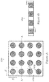
- FIG. 1A is a plan view of a structure with dielectric vias in one embodiment of the invention.
- FIG. 1B is a sectional view of the structure of FIG. 1A take along line A-A in FIG. 1A ;
- FIG. 2 is a flow chat of a method for making the structure of FIG. 1 ;
- FIG. 3 is a perspective view of a substrate-integrated waveguide in one embodiment of the invention.
- FIG. 4A is a plan view of a substrate-integrated dielectric resonator antenna in one embodiment of the invention.
- FIG. 4B is a sectional view of the substrate-integrated dielectric resonator antenna take along line Y-Y in FIG. 4A ;
- FIG. 5 is a plot showing the electric field distribution of the substrate-integrated dielectric resonator antenna of FIG. 4A ;
- FIG. 6A is a graph showing the simulated change in reflection coefficient (dB) with frequency (Hz) for different slot lengths in the substrate-integrated dielectric resonator antenna of FIG. 4A ;
- FIG. 6B is a graph showing the simulated change in realized gain (dBi) with frequency (Hz) for the substrate-integrated dielectric resonator antenna of FIG. 4A ;
- FIG. 7A is a plot showing the simulated radiation pattern of the substrate-integrated dielectric resonator antenna of FIG. 4A in the E-plane.
- FIG. 7B is a plot showing the simulated radiation pattern of the substrate-integrated dielectric resonator antenna of FIG. 4A in the H-plane.
- FIGS. 1A and 1B show a structure too with dielectric vias 104 in plan view.
- the structure too can be used to confine or guide electromagnetic energy.
- the structure too includes a substrate layer 102 with a first dielectric constant.
- the substrate layer 102 may be formed of a substrate material used in printed circuit boards, and the first dielectric constant may be around 2 to around 4.
- sixteen dielectric vias 104 are arranged in the substrate layer 102 , in a 4 ⁇ 4 array.
- Each of the dielectric vias 104 includes a via-hole of circular cross section and diameter d extending through the substrate layer 102 and a dielectric material 106 filled inside the via-hole.
- the dielectric material 106 filling the via-hole has a dielectric constant (relative permittivity) that is at least two times the dielectric constant of the substrate layer 102 .
- the first dielectric constant is at least 2 and the second dielectric constant is at least 4.
- the second dielectric constant can be at least to, at least 15, or at least 20.
- the dielectric material 106 includes perovskite oxide.
- Example of perovskite oxide includes Barium Titanate, Barium Strontium Titanate, Lead ZirconateTitanate, and Lead Lanthanum ZirconateTitanate.
- the dielectric material 106 may be in the form of a paste retained in the via-hole, or may be in the form of a solid solidified from an initial paste form.
- the paste includes perovskite oxide particles.
- Example of perovskite oxide particles include one or more of: Barium Titanate particles, Barium Strontium Titanate particles, Lead ZirconateTitanate particles, and Lead Lanthanum ZirconateTitanate particles.
- the perovskite oxide particles are sized in one dimension between 30 nm to 2000 nm. On average, the perovskite oxide particles can be sized in one dimension between 30 nm to 2000 nm.
- the structure too may further include two material layers, one on each side of the substrate, to enclose the via-holes hence retain the dielectric materials 106 in the via-holes. These two material layers may be a prepreg, a metallic layer, or a dielectric layer with the dielectric material same as that filled in the via-holes.
- the dielectric vias 104 act as electric walls that provide a highly reflective boundary for confining or directing electromagnetic energy impinging on the walls.
- the structure 100 has a unit cell size of S ⁇ S.
- the structure 100 in FIG. 1 can be incorporated or can form a substrate-integrated device.
- the substrate-integrated device include: microwave device, printed circuit board, substrate-integrated waveguide, substrate-integrated dielectric resonator (which may be part of a substrate-integrated dielectric resonator antenna or filter).
- the substrate-integrated device is preferably arranged to operate at radio frequency or microwave range.
- FIG. 2 shows a method 200 for making the structure of FIG. 1 in one embodiment of the invention.
- the method 200 begins in step 202 , in which one or more via-holes 106 are arranged in the substrate layer 102 with the first dielectric constant.
- the via-holes may be arranged in the substrate layer by cutting, drilling, or the like.
- the method proceeds to step 204 , in which the dielectric material 106 with the second dielectric constant is arranged in the via-holes, to form the structure 100 .
- Step 204 may involve coating the via-hole with the dielectric material 106 .
- step 204 may involve filling the via-hole partly or completely with the dielectric material 106 .
- step 204 includes arranging a paste with the dielectric material 106 and optionally a solvent in the via-holes.
- the paste may include pre-sintered perovskite oxide particles and a solvent.
- the pre-sintered perovskite oxide particles may include one or more of: Barium Titanate particles, Barium Strontium Titanate particles, Lead ZirconateTitanate particles, and Lead Lanthanum ZirconateTitanate particles; while the solvent may include one or more of: Xylene, Toluene, and Tetrahydrofuran.
- the paste may be heated to evaporate the solvent and solidify the dielectric material 106 so as to attach the dielectric material 106 to the substrate 102 .
- the paste may be enclosed in the via-holes by two material layers one on each side of the substrate (and each end of the via-hole). The two material layers may be a prepreg, a metallic layer, or a dielectric layer with the dielectric material 106 .
- FIG. 3 shows a substrate-integrated waveguide (SIW) 300 in one embodiment of the invention.
- the waveguide 300 has a similar basic structure as the structure 100 of FIG. 1 .
- the waveguide includes an upper metallic layer (very thin) 301 , a middle substrate layer 302 , and a lower metallic layer (very thin) 303 .
- Dielectric vias 304 of circular cross sectional and diameter d are arranged in the middle substrate layer 302 .
- the dielectric vias 304 are arranged in two parallel rows. The dielectric vias 304 in the same row are spaced apart generally equally, with a separation (pitch, distance between cross sectional centers of adjacent vias in the same row) S.
- the two rows are separate by a separation (distance between cross sectional centers of corresponding vias) W.
- the space between the two parallel rows of the dielectric vias 304 defines a wave guiding channel 306 .
- further dielectric vias can be arranged between the two rows to provide filtering function.
- FIGS. 4A and 4B show a substrate-integrated dielectric resonator antenna 400 in one embodiment of the invention.
- the dielectric resonator antenna 400 has a similar basic structure as the structure 100 of FIG. 1 .
- the dielectric resonator antenna 400 includes a first upper substrate layer 402 with a first dielectric constant.
- An array of dielectric vias 404 is arranged in the first upper substrate layer 402 .
- the array of dielectric vias 404 resembles the shape of a dielectric resonator.
- Each dielectric via 404 includes a via-hole formed in the substrate layer 402 and a dielectric material 406 filled in the via-hole.
- the dielectric constant of the dielectric material 406 is at least two times the dielectric constant of the substrate 402 .
- the dielectric resonator antenna 400 also has a ground plane 405 arranged below the first substrate layer 402 .
- a second substrate layer 407 containing a feeding mechanism is attached to the first substrate layer 402 via the ground plane 405 .
- the feeding mechanism includes a slot (see FIG. 4A , horizontal rectangle in dotted line) and a microstrip line 409 attached to the bottom of the second substrate layer 407 .
- the slot is arranged in the ground plane.
- the microstrip overlaps with some of the dielectric vias 404 in plan view.
- the dielectric resonator antenna 400 is excited by the slot of width W and length L which is fed by the microstrip line of width W f .
- the dielectric resonator antenna 400 in this embodiment can be excited to various operation modes, including but not limited to HEM11 ⁇ mode.
- FIG. 5 shows a simulated electric field pattern of the substrate-integrated dielectric resonator antenna 400 . As shown in FIG. 5 , the field distribution resembles the regular HEM11 ⁇ mode of a regular, solid dielectric resonator antenna.
- FIG. 6A shows the simulated change in reflection coefficient (dB) with frequency (Hz) for different lengths (6 mm, 7 mm, 8 mm) of the slot in the substrate-integrated dielectric resonator antenna 400 .
- FIG. 6B shows the simulated change in realized gain (dBi) with frequency (Hz) for the substrate-integrated dielectric resonator antenna 400 .
- the antenna 400 attains a realized gain of 6 dBi at 10 GHz, which is reasonable for a DRA operating in HEM11 ⁇ mode.
- the antenna 400 has a ⁇ 10 dB bandwidth of 11%.
- FIGS. 7A and 7B show the simulated radiation pattern of the substrate-integrated dielectric resonator antenna 400 in the E-plane and the H-plane respectively. As shown in FIGS. 7A and 7B , the pattern is omnidirectional as expected from a dielectric resonator antenna operating in the HEM11 ⁇ mode.
- the arrangement of dielectric vias as disclosed allow for customization of substrates such as PCB substrates, and for confining and directing electromagnetic energy.
- the substrate-integrated dielectric resonator antenna embodiment by integrating the dielectric resonator antenna to the substrate using the dielectric vias, eliminates the problem associated with conventional inaccurate placement of dielectric resonator antenna on top of PCB substrate.
- the structure with the dielectric vias e.g., microwave circuits and substrate-integrated dielectric resonator antenna
- Other devices such as filters and oscillators can be manufactured in substrate, improving space efficiency and reducing the footprint for electronic components.
- ceramic, pre-sintered perovskite oxide particles eliminate the need for high temperature sintering, thereby preventing damage to the substrate layer.
- various devices or microwave devices such as substrate-integrated waveguides (SIW), cavities, dielectric resonators, filters, resonating oscillators tank or substrate-integrated dielectric resonator antennas can be designed, with or without other metallic vias or dielectric/metal track.
- SIW substrate-integrated waveguides
- the losses occurring in the metallic sidewalls can be spared. This can be especially helpful when operating such a device at radio frequency ranges.
- the shape and form of the substrate or substrate layer can be varied.
- the thickness of the substrate layer need not be constant.
- the number, position, shape (e.g., cross sectional), and arrangement of dielectric vias in the substrate can be varied.
- the dielectric vias may be arranged in a regular pattern, e.g., one that has an axis of symmetry, or may be arranged in a random, irregular pattern.
- the dielectric vias need not be completely filled with dielectric material. Instead, it could be filled partly with or coated with the dielectric material.
- the dielectric constant of the substrate and the dielectric constant of the dielectric material can take other values, depending on applications, so long as the dielectric constant of the dielectric material is larger than the dielectric constant of the substrate.
- the dielectric material can be fixed or retained or enclosed in the via-holes using various chemical or mechanical means, not limited to heating or enclosing with material layers as provided above.
- the upper and lower metallic layers in FIG. 3 can be replaced by the dielectric material (paste form or solid form) serving as electric wall.
- the dielectric resonator antenna can be excited in various ways, not necessarily by or via the slot.
Landscapes
- Engineering & Computer Science (AREA)
- Microelectronics & Electronic Packaging (AREA)
- Manufacturing & Machinery (AREA)
- Production Of Multi-Layered Print Wiring Board (AREA)
- Control Of Motors That Do Not Use Commutators (AREA)
Abstract
A substrate-integrated device includes a substrate layer with a first dielectric constant and one or more dielectric vias, the one or more dielectric vias each includes a via-hole extending through the substrate layer, and a dielectric material with a second dielectric constant contained within the via-hole. The second dielectric constant is larger than, preferably at least two times, the first dielectric constant.
Description
The invention relates to a substrate-integrated device and a method for making a substrate-integrated device.
A via is an electrical connection between different layers in an electronic circuit. Conventional vias are metallic vias in the form of a “metallized” hole (i.e., a hole coated with a metallic material) in a substrate.
Metallic vias are commonly used in RF (such as PCB applications) and IC technologies. In RF technology, metallic via-holes are used in place of solid metallic walls. In IC technology, metallic vias are used to electrically connect different layers of substrates with each other. Problematically, however, these metallic vias may suffer from high loss in some applications, such as applications as microwave frequencies. Also, the process for “metallizing” the holes to produce the vias can be time-consuming and costly.
In accordance with a first aspect of the invention, there is provided a substrate-integrated device, having: a substrate layer with a first dielectric constant and one or more dielectric vias. The one or more dielectric vias each having a via-hole extending through the substrate layer, and a dielectric material with a second dielectric constant contained within the via-hole. The second dielectric constant (relative permittivity) is larger than the first dielectric constant. Preferably, the second dielectric constant is at least two times, at least three times, at least four times, at least five times, or at least ten times of the first dielectric constant.
In one embodiment of the first aspect, the via-hole is filled substantially completely with the dielectric material.
In one embodiment of the first aspect, the first electric constant is at least 2 and the second dielectric constant is at least 4. Preferably, the second dielectric constant is at least 10, at least 15, or at least 20.
In one embodiment of the first aspect, the one or more dielectric vias includes a plurality of dielectric vias. The plurality of dielectric vias may be arranged regularly or randomly. The plurality of dielectric vias may be spaced apart evenly. In one example, the plurality of dielectric vias includes dielectric vias arranged in at least two parallel rows, each of the two parallel rows having two or more dielectric vias. One or more dielectric vias may further be arranged between the two parallel rows. In one example, two adjacent parallel rows of dielectric vias define, between the two rows, a wave guiding channel.
In one embodiment of the first aspect, the dielectric material includes perovskite oxide. The perovskite oxide may include one or more of: Barium Titanate, Barium Strontium Titanate, Lead ZirconateTitanate, and Lead Lanthanum ZirconateTitanate.
In one embodiment of the first aspect, the dielectric material is in the form of a paste. In one example, the paste includes perovskite oxide particles. The perovskite oxide particles may include one or more of: Barium Titanate particles, Barium Strontium Titanate particles, Lead ZirconateTitanate particles, and Lead Lanthanum ZirconateTitanate particles. The perovskite oxide particles may be sized between 30 nm to 2000 nm, or they may have an average size between 30 nm to 2000 nm.
In one embodiment of the first aspect, the substrate-integrated device further includes a first material layer arranged on one side of the substrate layer. The first material layer may include a prepreg, a metallic layer, or a dielectric layer with the dielectric material.
In one embodiment of the first aspect, the substrate-integrated device further includes a second material layer arranged on the other side of the substrate layer. The second material layer may include a prepreg, a metallic layer, or a dielectric layer with the dielectric material.
In one embodiment of the first aspect, the substrate-integrated device is a microwave device.
In one embodiment of the first aspect, the substrate-integrated device is a printed circuit board.
In one embodiment of the first aspect, the substrate-integrated device is a substrate-integrated waveguide.
In one embodiment of the first aspect, the substrate-integrated device is a substrate-integrated dielectric resonator.
In one embodiment of the first aspect, the substrate-integrated dielectric resonator is part of a substrate-integrated dielectric resonator antenna.
In one embodiment of the first aspect, the substrate-integrated dielectric resonator is part of a substrate-integrated dielectric resonator filter.
In one embodiment of the first aspect, the substrate-integrated device is arranged to operate at radio frequency range.
In accordance with a second aspect of the invention, there is provided a method for making a substrate-integrated device, comprising: arranging, in one or more via-holes of a substrate layer with a first dielectric constant, a dielectric material with a second dielectric constant, thereby forming one or more dielectric vias. The one or more dielectric vias each having a via-hole formed in the substrate layer, and a dielectric material with a second dielectric constant contained within the via-hole. The second dielectric constant is larger than the first dielectric constant. Preferably, the second dielectric constant is at least two times, at least three times, at least four times, at least five times, or at least ten times of the first dielectric constant.
In one embodiment of the second aspect, arranging the dielectric material in the one or more via-holes includes: filling the one or more via-holes substantially completely with the dielectric material.
In one embodiment of the second aspect, the first dielectric constant is at least 2 and the second dielectric constant is at least 4. Preferably, the second dielectric constant is at least 10, at least 15, or at least 20.
In one embodiment of the second aspect, the dielectric material comprises perovskite oxide. The perovskite oxide may include one or more of: Barium Titanate, Barium Strontium Titanate, Lead ZirconateTitanate, and Lead Lanthanum ZirconateTitanate.
In one embodiment of the second aspect, arranging the dielectric material in the one or more via-holes includes: arranging a paste including the dielectric material in the one or more via-holes.
In one embodiment of the second aspect, the paste comprises pre-sintered perovskite oxide particles and a solvent. The pre-sintered perovskite oxide particles may include one or more of: Barium Titanate particles, Barium Strontium Titanate particles, Lead ZirconateTitanate particles, and Lead Lanthanum ZirconateTitanate particles. The solvent may include one or more of: Xylene, Toluene, and Tetrahydrofuran. The perovskite oxide particles may be sized between 30 nm to 2000 nm, or they may have an average size between 30 nm to 2000 nm.
In one embodiment of the second aspect, arranging the dielectric material in the one or more via-holes further includes: heating the paste to evaporate the solvent and attach the dielectric material to the substrate.
In one embodiment of the second aspect, arranging the dielectric material in the one or more via-holes further includes: enclosing the one or more via-holes to retain the paste in the one or more via-holes.
In one embodiment of the second aspect, enclosing the one or more via-holes includes: arranging a first material layer on one side of the substrate and at a first end of the one or more via-holes and arranging a second material layer on another side of the substrate and at a second end of the one or more via-holes to enclose the one or more via-holes. The first material layer and the second material layer each includes a prepreg, a metallic layer, or a dielectric layer with the dielectric material.
In accordance with a third aspect of the invention, there is provided a substrate-integrated device made using the method of the second aspect.
In accordance with a fourth aspect of the invention, there is provided a structure for confining electromagnetic energy, having: a substrate layer with a first dielectric constant and one or more dielectric vias. The one or more dielectric vias each having a via-hole extending through the substrate layer, and a dielectric material with a second dielectric constant contained within the via-hole. The second dielectric constant (relative permittivity) is larger than the first dielectric constant. Preferably, the second dielectric constant is at least two times, at least three times, at least four times, at least five times, or at least ten times of the first dielectric constant.
In one embodiment of the fourth aspect, the via-hole is filled substantially completely with the dielectric material.
In one embodiment of the fourth aspect, the first dielectric constant is at least 2 and the second dielectric constant is at least 4. Preferably, the second dielectric constant is at least 10, at least 15, or at least 20.
In one embodiment of the fourth aspect, the one or more dielectric vias includes a plurality of dielectric vias. The plurality of dielectric vias may be arranged regularly or randomly. The plurality of dielectric vias may be spaced apart evenly. In one example, the plurality of dielectric vias includes dielectric vias arranged in at least two parallel rows, each of the two parallel rows having two or more dielectric vias. One or more dielectric vias may further be arranged between the two parallel rows. In one example, two adjacent parallel rows of dielectric vias define, between the two rows, a wave guiding channel.
In one embodiment of the fourth aspect, the dielectric material includes perovskite oxide. The perovskite oxide may include one or more of: Barium Titanate, Barium Strontium Titanate, Lead ZirconateTitanate, and Lead Lanthanum ZirconateTitanate.
In one embodiment of the fourth aspect, the dielectric material is in the form of a paste. In one example, the paste includes perovskite oxide particles. The perovskite oxide particles may include one or more of: Barium Titanate particles, Barium Strontium Titanate particles, Lead ZirconateTitanate particles, and Lead Lanthanum ZirconateTitanate particles. The perovskite oxide particles may be sized between 30 nm to 2000 nm, or they may have an average size between 30 nm to 2000 nm.
In one embodiment of the fourth aspect, the structure further includes a first material layer arranged on one side of the substrate layer. The first material layer may include a prepreg, a metallic layer, or a dielectric layer with the dielectric material.
In one embodiment of the fourth aspect, the structure further includes a second material layer arranged on the other side of the substrate layer. The second material layer may include a prepreg, a metallic layer, or a dielectric layer with the dielectric material.
In accordance with a fifth aspect of the invention, there is provided a microwave device including the structure of the fourth aspect.
In accordance with a sixth aspect of the invention, there is provided a substrate-integrated waveguide including the structure of the fourth aspect.
In accordance with a seventh aspect of the invention, there is provided a substrate-integrated dielectric resonator including the structure of the fourth aspect.
In accordance with a eighth aspect of the invention, there is provided a substrate-integrated dielectric resonator antenna including the structure of the fourth aspect.
In accordance with a eighth aspect of the invention, there is provided a substrate-integrated dielectric resonator filter including the structure of the fourth aspect.
In accordance with a ninth aspect of the invention, there is provided a substrate-integrated dielectric resonator antenna, including a first substrate layer with a first dielectric constant; one or more dielectric vias each having a via-hole formed in the substrate layer, and a dielectric material with a second dielectric constant contained within the via-hole, the second dielectric constant is larger than (e.g., at least two times) the first dielectric constant; a ground plane arranged on one side of the first substrate layer; a second substrate layer attached to the first substrate layer via the ground plane; and a microstrip line attached to the second substrate layer on a side opposite to the ground plane. Preferably, in plan view, the microstrip at least partly overlaps with the one or more dielectric vias and with a slot formed in the ground plane.
In accordance with a tenth aspect of the invention, there is provided a printed circuit board including the structure of the fourth aspect.
Embodiments of the invention will now be described, by way of example, with reference to the accompanying drawings in which:
In this embodiment, the dielectric material 106 includes perovskite oxide. Example of perovskite oxide includes Barium Titanate, Barium Strontium Titanate, Lead ZirconateTitanate, and Lead Lanthanum ZirconateTitanate. The dielectric material 106 may be in the form of a paste retained in the via-hole, or may be in the form of a solid solidified from an initial paste form. In one example, the paste includes perovskite oxide particles. Example of perovskite oxide particles include one or more of: Barium Titanate particles, Barium Strontium Titanate particles, Lead ZirconateTitanate particles, and Lead Lanthanum ZirconateTitanate particles. The perovskite oxide particles are sized in one dimension between 30 nm to 2000 nm. On average, the perovskite oxide particles can be sized in one dimension between 30 nm to 2000 nm. In the example that the dielectric material 106 is a paste, the structure too may further include two material layers, one on each side of the substrate, to enclose the via-holes hence retain the dielectric materials 106 in the via-holes. These two material layers may be a prepreg, a metallic layer, or a dielectric layer with the dielectric material same as that filled in the via-holes.
In the structure 100, the dielectric vias 104 act as electric walls that provide a highly reflective boundary for confining or directing electromagnetic energy impinging on the walls. The structure 100 has a unit cell size of S×S.
The structure 100 in FIG. 1 can be incorporated or can form a substrate-integrated device. Examples of the substrate-integrated device include: microwave device, printed circuit board, substrate-integrated waveguide, substrate-integrated dielectric resonator (which may be part of a substrate-integrated dielectric resonator antenna or filter). The substrate-integrated device is preferably arranged to operate at radio frequency or microwave range.
Various methods can be used to attach or otherwise fix the dielectric material 106 to the substrate 102. In one example, the paste may be heated to evaporate the solvent and solidify the dielectric material 106 so as to attach the dielectric material 106 to the substrate 102. In another example, the paste may be enclosed in the via-holes by two material layers one on each side of the substrate (and each end of the via-hole). The two material layers may be a prepreg, a metallic layer, or a dielectric layer with the dielectric material 106.
The structure and device of the above embodiments are advantageous in various aspects. First, the arrangement of dielectric vias as disclosed allow for customization of substrates such as PCB substrates, and for confining and directing electromagnetic energy. The substrate-integrated dielectric resonator antenna embodiment, by integrating the dielectric resonator antenna to the substrate using the dielectric vias, eliminates the problem associated with conventional inaccurate placement of dielectric resonator antenna on top of PCB substrate. The structure with the dielectric vias (e.g., microwave circuits and substrate-integrated dielectric resonator antenna) can be made simply and cost effectively. Other devices such as filters and oscillators can be manufactured in substrate, improving space efficiency and reducing the footprint for electronic components. The use of ceramic, pre-sintered perovskite oxide particles in some embodiments eliminate the need for high temperature sintering, thereby preventing damage to the substrate layer. Utilizing the highly reflective boundary of the wall of dielectric vias, various devices or microwave devices such as substrate-integrated waveguides (SIW), cavities, dielectric resonators, filters, resonating oscillators tank or substrate-integrated dielectric resonator antennas can be designed, with or without other metallic vias or dielectric/metal track. By utilizing the dielectric vias in the substrate-integrated waveguides, the losses occurring in the metallic sidewalls can be spared. This can be especially helpful when operating such a device at radio frequency ranges.
It will be appreciated by persons skilled in the art that numerous variations and/or modifications may be made to the invention as shown in the specific embodiments without departing from the spirit or scope of the invention as broadly described. The described embodiments of the invention should therefore be considered in all respects as illustrative, not restrictive.
For example, the shape and form of the substrate or substrate layer can be varied. The thickness of the substrate layer need not be constant. The number, position, shape (e.g., cross sectional), and arrangement of dielectric vias in the substrate can be varied. In some examples, there can be only one dielectric vias. The dielectric vias may be arranged in a regular pattern, e.g., one that has an axis of symmetry, or may be arranged in a random, irregular pattern. The dielectric vias need not be completely filled with dielectric material. Instead, it could be filled partly with or coated with the dielectric material. The dielectric constant of the substrate and the dielectric constant of the dielectric material can take other values, depending on applications, so long as the dielectric constant of the dielectric material is larger than the dielectric constant of the substrate. The dielectric material can be fixed or retained or enclosed in the via-holes using various chemical or mechanical means, not limited to heating or enclosing with material layers as provided above. The upper and lower metallic layers in FIG. 3 can be replaced by the dielectric material (paste form or solid form) serving as electric wall. The dielectric resonator antenna can be excited in various ways, not necessarily by or via the slot.
Claims (34)
1. A substrate-integrated dielectric resonator, comprising:
a substrate layer with a first dielectric constant; and
a plurality of dielectric vias each having
a via-hole extending through the substrate layer, and
a dielectric material with a second dielectric constant contained within the via-hole;
wherein the second dielectric constant is larger than the first dielectric constant.
2. The substrate-integrated dielectric resonator of claim 1 , wherein the via-holes are filled substantially completely with the dielectric material.
3. The substrate-integrated dielectric resonator of claim 1 , wherein the first dielectric constant is at least 2 and the second dielectric constant is at least 4.
4. The substrate-integrated dielectric resonator of claim 1 , wherein the plurality of dielectric vias comprises dielectric vias arranged in at least two parallel rows, each of the two parallel rows having two or more dielectric vias.
5. The substrate-integrated dielectric resonator of claim 4 , wherein the plurality of dielectric vias further comprises one or more dielectric vias arranged between the two parallel rows.
6. The substrate-integrated dielectric resonator of claim 4 , wherein a wave guiding channel is defined between two adjacent parallel rows.
7. The substrate-integrated dielectric resonator of claim 1 , wherein the dielectric material comprises perovskite oxide.
8. The substrate-integrated dielectric resonator of claim 7 , wherein the perovskite oxide comprise one or more of: Barium Titanate, Barium Strontium Titanate, Lead ZirconateTitanate, and Lead Lanthanum ZirconateTitanate.
9. The substrate-integrated dielectric resonator of claim 1 , wherein the dielectric material is in the form of a paste; and wherein the paste comprises perovskite oxide particles.
10. The substrate-integrated dielectric resonator of claim 9 , wherein the perovskite oxide particles comprise one or more of: Barium Titanate particles, Barium Strontium Titanate particles, Lead ZirconateTitanate particles, and Lead Lanthanum ZirconateTitanate particles.
11. The substrate-integrated dielectric resonator of claim 9 , wherein the perovskite oxide particles are sized between 30 nm to 2000 nm.
12. The substrate-integrated dielectric resonator of claim 9 , wherein the perovskite oxide particles has an average size between 30 nm to 2000 nm.
13. The substrate-integrated dielectric resonator of claim 1 , further comprising a first material layer arranged on one side of the substrate layer.
14. The substrate-integrated dielectric resonator of claim 13 , wherein the first material layer comprises a prepreg, a metallic layer, or a dielectric layer with the dielectric material.
15. The substrate-integrated dielectric resonator of claim 13 , further comprising a second material layer arranged on the other side of the substrate layer.
16. The substrate-integrated dielectric resonator of claim 15 , wherein the second material layer comprises a prepreg, a metallic layer, or a dielectric layer with the dielectric material.
17. The substrate-integrated dielectric resonator of claim 1 , wherein the substrate-integrated dielectric resonator is arranged to operate at radio frequency range.
18. The substrate-integrated dielectric resonator of claim 1 , wherein the substrate-integrated dielectric resonator is part of a substrate-integrated dielectric resonator antenna.
19. The substrate-integrated dielectric resonator of claim 1 , wherein the substrate-integrated dielectric resonator is part of a substrate-integrated dielectric resonator filter.
20. The substrate-integrated dielectric resonator of claim 1 , wherein the plurality of dielectric vias are spaced apart evenly.
21. The substrate-integrated dielectric resonator of claim 1 , wherein the second dielectric constant is at least two times the first dielectric constant.
22. A method for making a substrate-integrated dielectric resonator, comprising:
arranging, in a plurality of via-holes of a substrate layer with a first dielectric constant, a dielectric material with a second dielectric constant, thereby forming a plurality of dielectric vias each having
a via-hole formed in the substrate layer, and
a dielectric material with a second dielectric constant contained within the via-hole;
wherein the second dielectric constant is larger than the first dielectric constant.
23. The method of claim 22 , wherein arranging the dielectric material in the plurality of via-holes comprises:
filling the plurality of via-holes substantially completely with the dielectric material.
24. The method of claim 22 , wherein the first dielectric constant is at least 2 and the second dielectric constant is at least 4.
25. The method of claim 22 , wherein the dielectric material comprises perovskite oxide.
26. The method of claim 25 , wherein the perovskite oxide comprise one or more of: Barium Titanate, Barium Strontium Titanate, Lead ZirconateTitanate, and Lead Lanthanum ZirconateTitanate.
27. The method of claim 22 , wherein arranging the dielectric material in the plurality of via-holes comprises:
arranging a paste including the dielectric material in the plurality of via-holes.
28. The method of claim 27 , wherein the paste comprises pre-sintered perovskite oxide particles and a solvent.
29. The method of claim 28 , wherein the pre-sintered perovskite oxide particles comprise one or more of: Barium Titanate particles, Barium Strontium Titanate particles, Lead ZirconateTitanate particles, and Lead Lanthanum ZirconateTitanate particles.
30. The method of claim 28 , wherein the solvent comprises one or more of: Xylene, Toluene, and Tetrahydrofuran.
31. The method of claim 27 , wherein arranging the dielectric material in the plurality of via-holes further comprises:
heating the paste to evaporate the solvent and attach the dielectric material to the substrate.
32. The method of claim 27 , wherein arranging the dielectric material in the plurality of via-holes further comprises:
enclosing the one or more via-holes to retain the paste in the plurality of via-holes.
33. The method of claim 32 , wherein enclosing the plurality of via-holes includes:
arranging a first material layer on one side of the substrate and at a first end of the plurality of via-holes and arranging a second material layer on another side of the substrate and at a second end of the plurality of via-holes to enclose the plurality of via-holes.
34. The method of claim 33 , wherein the first material layer and the second material layer each comprises a prepreg, a metallic layer, or a dielectric layer with the dielectric material.
Priority Applications (1)
| Application Number | Priority Date | Filing Date | Title |
|---|---|---|---|
| US16/502,125 US10856408B1 (en) | 2019-07-03 | 2019-07-03 | Substrate-integrated device and method for making the same |
Applications Claiming Priority (1)
| Application Number | Priority Date | Filing Date | Title |
|---|---|---|---|
| US16/502,125 US10856408B1 (en) | 2019-07-03 | 2019-07-03 | Substrate-integrated device and method for making the same |
Publications (1)
| Publication Number | Publication Date |
|---|---|
| US10856408B1 true US10856408B1 (en) | 2020-12-01 |
Family
ID=73554947
Family Applications (1)
| Application Number | Title | Priority Date | Filing Date |
|---|---|---|---|
| US16/502,125 Active US10856408B1 (en) | 2019-07-03 | 2019-07-03 | Substrate-integrated device and method for making the same |
Country Status (1)
| Country | Link |
|---|---|
| US (1) | US10856408B1 (en) |
Cited By (3)
| Publication number | Priority date | Publication date | Assignee | Title |
|---|---|---|---|---|
| US20220272835A1 (en) * | 2021-02-22 | 2022-08-25 | Kabushiki Kaisha Toshiba | Substrate, electronic circuit, antenna apparatus, electronic apparatus, and method for producing a substrate |
| US11575203B1 (en) * | 2021-10-04 | 2023-02-07 | City University Of Hong Kong | 3-d printed wideband high-gain circularly-polarized dielectric resonator antenna |
| US20230318187A1 (en) * | 2022-04-05 | 2023-10-05 | City University Of Hong Kong | Compact wideband low-profile dielectric resonator antennas |
Citations (8)
| Publication number | Priority date | Publication date | Assignee | Title |
|---|---|---|---|---|
| US5354599A (en) | 1992-09-24 | 1994-10-11 | Hughes Aircraft Company | Dielectric vias within multi-layer 3-dimensional structures/substrates |
| US20020179332A1 (en) * | 2001-05-29 | 2002-12-05 | Mitsubishi Denki Kabushiki Kaisha | Wiring board and a method for manufacturing the wiring board |
| US20090297804A1 (en) * | 2006-04-18 | 2009-12-03 | Florian Paul | Ceramic dielectric or thin and/or thick layers containing at least one ceramic dielectric method for production and use thereof |
| US20130199834A1 (en) * | 2010-06-29 | 2013-08-08 | Fci | Structured circuit board and method |
| US20140097918A1 (en) | 2012-10-09 | 2014-04-10 | International Business Machines Corporation | Printed circuit board having dc blocking dielectric waveguide vias |
| US20170009090A1 (en) | 2015-07-06 | 2017-01-12 | University Of Massachusetts | Ferroelectric nanocomposite based dielectric inks for reconfigurable rf and microwave applications |
| US20180027648A1 (en) * | 2016-02-04 | 2018-01-25 | Taiwan Semiconductor Manufacturing Co., Ltd. | Interconnect structure and method of manufacturing the same |
| US20180177041A1 (en) | 2016-12-21 | 2018-06-21 | Invensas Corporation | Surface Integrated Waveguides and Circuit Structures Therefor |
-
2019
- 2019-07-03 US US16/502,125 patent/US10856408B1/en active Active
Patent Citations (8)
| Publication number | Priority date | Publication date | Assignee | Title |
|---|---|---|---|---|
| US5354599A (en) | 1992-09-24 | 1994-10-11 | Hughes Aircraft Company | Dielectric vias within multi-layer 3-dimensional structures/substrates |
| US20020179332A1 (en) * | 2001-05-29 | 2002-12-05 | Mitsubishi Denki Kabushiki Kaisha | Wiring board and a method for manufacturing the wiring board |
| US20090297804A1 (en) * | 2006-04-18 | 2009-12-03 | Florian Paul | Ceramic dielectric or thin and/or thick layers containing at least one ceramic dielectric method for production and use thereof |
| US20130199834A1 (en) * | 2010-06-29 | 2013-08-08 | Fci | Structured circuit board and method |
| US20140097918A1 (en) | 2012-10-09 | 2014-04-10 | International Business Machines Corporation | Printed circuit board having dc blocking dielectric waveguide vias |
| US20170009090A1 (en) | 2015-07-06 | 2017-01-12 | University Of Massachusetts | Ferroelectric nanocomposite based dielectric inks for reconfigurable rf and microwave applications |
| US20180027648A1 (en) * | 2016-02-04 | 2018-01-25 | Taiwan Semiconductor Manufacturing Co., Ltd. | Interconnect structure and method of manufacturing the same |
| US20180177041A1 (en) | 2016-12-21 | 2018-06-21 | Invensas Corporation | Surface Integrated Waveguides and Circuit Structures Therefor |
Cited By (5)
| Publication number | Priority date | Publication date | Assignee | Title |
|---|---|---|---|---|
| US20220272835A1 (en) * | 2021-02-22 | 2022-08-25 | Kabushiki Kaisha Toshiba | Substrate, electronic circuit, antenna apparatus, electronic apparatus, and method for producing a substrate |
| US11924967B2 (en) * | 2021-02-22 | 2024-03-05 | Kabushiki Kaisha Toshiba | Substrate, electronic circuit, antenna apparatus, electronic apparatus, and method for producing a substrate |
| US11575203B1 (en) * | 2021-10-04 | 2023-02-07 | City University Of Hong Kong | 3-d printed wideband high-gain circularly-polarized dielectric resonator antenna |
| US20230318187A1 (en) * | 2022-04-05 | 2023-10-05 | City University Of Hong Kong | Compact wideband low-profile dielectric resonator antennas |
| US11929563B2 (en) * | 2022-04-05 | 2024-03-12 | City University Of Hong Kong | Compact wideband low-profile dielectric resonator antennas |
Similar Documents
| Publication | Publication Date | Title |
|---|---|---|
| JP6857793B2 (en) | Slot antenna with cavity with in-cavity resonator | |
| US9184505B2 (en) | Dielectric cavity antenna | |
| US8159413B2 (en) | Double-stacked EBG structure | |
| KR101571345B1 (en) | 2 system for interconnecting two substrates each comprising at least one transmission line | |
| US10856408B1 (en) | Substrate-integrated device and method for making the same | |
| US7746191B2 (en) | Waveguide to microstrip line transition having a conductive footprint for providing a contact free element | |
| EP1942557A1 (en) | High-frequency electromagnetic bandgap device and method for making same | |
| US7292204B1 (en) | Dielectric resonator antenna with a caved well | |
| US20210336316A1 (en) | Antenna array | |
| EP3637548A1 (en) | Planar array antenna and wireless communication module | |
| CN102084538A (en) | Waveguides and transmission lines in gaps between parallel conducting surfaces | |
| US10594041B2 (en) | Cavity backed slot antenna with in-cavity resonators | |
| CN110768014B (en) | Integrated substrate gap waveguide via cluster fed antenna | |
| WO2006097050A1 (en) | Integrated mm-wave planar array antenna with low loss feeding network | |
| CN105048051A (en) | Tunable substrate integrated waveguide circular resonant cavity filter | |
| CN201946751U (en) | Bragg grating array antenna based on half mode substrate integrated waveguide | |
| Kumar et al. | Design and optimization of slotted micro-machined patch antenna using composite substrate | |
| US12160043B2 (en) | Antenna device which is suitable for wireless communications according to a 5G network standard, RF transceiver containing an antenna device, and method for use in wireless communications according to a 5G network standard | |
| CN110364799A (en) | Double Ridge Integrated Substrate Gap Waveguide | |
| EP1933415A1 (en) | Electromagnetic bandgap motion sensor device and method for making same | |
| CN105655699B (en) | A kind of back of the body chamber gap circular polarized antenna using substrate integration wave-guide | |
| CN117080725A (en) | Dual-cavity three-resonant substrate integrated waveguide back cavity slot antenna | |
| CN110829032B (en) | Slot patch antenna based on integrated substrate gap waveguide | |
| CN207265226U (en) | The substrate of high radiation efficiency integrates medium resonator antenna array | |
| JP4713367B2 (en) | Aperture antenna |
Legal Events
| Date | Code | Title | Description |
|---|---|---|---|
| FEPP | Fee payment procedure |
Free format text: ENTITY STATUS SET TO UNDISCOUNTED (ORIGINAL EVENT CODE: BIG.); ENTITY STATUS OF PATENT OWNER: SMALL ENTITY |
|
| FEPP | Fee payment procedure |
Free format text: ENTITY STATUS SET TO SMALL (ORIGINAL EVENT CODE: SMAL); ENTITY STATUS OF PATENT OWNER: SMALL ENTITY |
|
| STCF | Information on status: patent grant |
Free format text: PATENTED CASE |
|
| MAFP | Maintenance fee payment |
Free format text: PAYMENT OF MAINTENANCE FEE, 4TH YR, SMALL ENTITY (ORIGINAL EVENT CODE: M2551); ENTITY STATUS OF PATENT OWNER: SMALL ENTITY Year of fee payment: 4 |